

STM690A, STM692A, STM703
STM704, STM802, STM805, STM817/8/9
5 V supervisor with battery switchover
Features
■ 5 V operating voltage
■ NVRAM supervisor for external LPSRAM
■ Chip-enable gating (STM818 only) for external
LPSRAM (7 ns max prop delay)
■ RST and RST outputs
■ 200 ms (typ) t
■
Watchdog timer - 1.6 sec (typ)
■ Automatic battery switchover
■ Low battery supply current - 0.4 µA (typ)
■ Power-fail comparator (PFI/PFO)
■ Low supply current - 40 µA (typ)
■ Guaranteed RST (RST) assertion down to
V
= 1.0 V
CC
■ Operating temperature:
–40 °C to +85 °C (industrial grade)
■ RoHS compliance
– Lead-free components are compliant with
the RoHS directive
rec
8
1
SO8 (M)
TSSOP8 3 x 3 (DS)
1. Contact local ST sales office for availability.
(1)
Table 1. Device summary
(1)
Battery
switch-
over
Power-fail
comparator
Chip-
enable
gating
Battery
freshness
seal
www.st.com
1
Manual
reset
input
Part number
STM690A ✓✓ ✓✓
STM692A ✓✓ ✓✓
STM703 ✓✓✓✓
STM704 ✓✓✓✓
STM802L/M ✓✓ ✓✓
STM805L ✓✓✓✓
STM817L/M ✓✓ ✓✓ ✓
STM818L/M ✓✓ ✓ ✓✓
STM819L/M ✓✓✓✓ ✓
1. All RST and RST outputs are push-pull.
August 2010 Doc ID 10522 Rev 10 1/43
Watchdog
input
Active-low
RST
(1)
Active-
high RST

Contents STM690A/692A/703/704/802/805/817/818/819
Contents
1 Description . . . . . . . . . . . . . . . . . . . . . . . . . . . . . . . . . . . . . . . . . . . . . . . . . 6
1.1 Pin descriptions . . . . . . . . . . . . . . . . . . . . . . . . . . . . . . . . . . . . . . . . . . . . . 8
1.1.1 MR . . . . . . . . . . . . . . . . . . . . . . . . . . . . . . . . . . . . . . . . . . . . . . . . . . . . . . 8
1.1.2 WDI . . . . . . . . . . . . . . . . . . . . . . . . . . . . . . . . . . . . . . . . . . . . . . . . . . . . . 8
1.1.3 RST
1.1.4 RST . . . . . . . . . . . . . . . . . . . . . . . . . . . . . . . . . . . . . . . . . . . . . . . . . . . . . 8
. . . . . . . . . . . . . . . . . . . . . . . . . . . . . . . . . . . . . . . . . . . . . . . . . . . . . 8
1.1.5 V
1.1.6 V
1.1.7 E . . . . . . . . . . . . . . . . . . . . . . . . . . . . . . . . . . . . . . . . . . . . . . . . . . . . . . . 9
1.1.8 E
1.1.9 PFI . . . . . . . . . . . . . . . . . . . . . . . . . . . . . . . . . . . . . . . . . . . . . . . . . . . . . . 9
1.1.10 PFO
OUT . . . . . . . . . . . . . . . . . . . . . . . . . . . . . . . . . . . . . . . . . . . . . . . . . . . . . . . . . . . . . . . . . . 9
BAT . . . . . . . . . . . . . . . . . . . . . . . . . . . . . . . . . . . . . . . . . . . . . . . . . . . . . . . . . . . . . . . . . . . 9
CON . . . . . . . . . . . . . . . . . . . . . . . . . . . . . . . . . . . . . . . . . . . . . . . . . . . . . . . . . . . . . . . . . . 9
. . . . . . . . . . . . . . . . . . . . . . . . . . . . . . . . . . . . . . . . . . . . . . . . . . . . . 9
2 Operation . . . . . . . . . . . . . . . . . . . . . . . . . . . . . . . . . . . . . . . . . . . . . . . . . 13
2.1 Reset output . . . . . . . . . . . . . . . . . . . . . . . . . . . . . . . . . . . . . . . . . . . . . . . 13
2.2 Push-button reset input (STM703/704/819) . . . . . . . . . . . . . . . . . . . . . . . 13
2.3 Watchdog input (NOT available on STM703/704/819) . . . . . . . . . . . . . . . 13
2.4 Backup battery switchover . . . . . . . . . . . . . . . . . . . . . . . . . . . . . . . . . . . . 14
2.5 Chip-enable gating (STM818 only) . . . . . . . . . . . . . . . . . . . . . . . . . . . . . . 15
2.6 Chip-enable input (STM818 only) . . . . . . . . . . . . . . . . . . . . . . . . . . . . . . . 15
2.7 Chip-enable output (STM818 only) . . . . . . . . . . . . . . . . . . . . . . . . . . . . . 15
2.8 Power-fail input/output (NOT available on STM818) . . . . . . . . . . . . . . . . 16
2.9 Applications information . . . . . . . . . . . . . . . . . . . . . . . . . . . . . . . . . . . . . . 16
2.10 Using a SuperCap™ as a backup power source . . . . . . . . . . . . . . . . . . . 17
2.11 Negative-going V
transients . . . . . . . . . . . . . . . . . . . . . . . . . . . . . . . . . 18
CC
2.12 Battery freshness seal (STM817/818/819) . . . . . . . . . . . . . . . . . . . . . . . . 19
3 Typical operating characteristics . . . . . . . . . . . . . . . . . . . . . . . . . . . . . 20
4 Maximum ratings . . . . . . . . . . . . . . . . . . . . . . . . . . . . . . . . . . . . . . . . . . . 31
5 DC and AC parameters . . . . . . . . . . . . . . . . . . . . . . . . . . . . . . . . . . . . . . 32
2/43 Doc ID 10522 Rev 10

STM690A/692A/703/704/802/805/817/818/819 Contents
6 Package mechanical data . . . . . . . . . . . . . . . . . . . . . . . . . . . . . . . . . . . . 37
7 Part numbering . . . . . . . . . . . . . . . . . . . . . . . . . . . . . . . . . . . . . . . . . . . . 40
8 Revision history . . . . . . . . . . . . . . . . . . . . . . . . . . . . . . . . . . . . . . . . . . . 42
Doc ID 10522 Rev 10 3/43

List of tables STM690A/692A/703/704/802/805/817/818/819
List of tables
Table 1. Device summary . . . . . . . . . . . . . . . . . . . . . . . . . . . . . . . . . . . . . . . . . . . . . . . . . . . . . . . . . . 1
Table 2. Signal names . . . . . . . . . . . . . . . . . . . . . . . . . . . . . . . . . . . . . . . . . . . . . . . . . . . . . . . . . . . . 7
Table 3. Pin description . . . . . . . . . . . . . . . . . . . . . . . . . . . . . . . . . . . . . . . . . . . . . . . . . . . . . . . . . . 10
Table 4. I/O status in battery backup . . . . . . . . . . . . . . . . . . . . . . . . . . . . . . . . . . . . . . . . . . . . . . . . 14
Table 5. Absolute maximum ratings . . . . . . . . . . . . . . . . . . . . . . . . . . . . . . . . . . . . . . . . . . . . . . . . . 31
Table 6. Operating and AC measurement conditions. . . . . . . . . . . . . . . . . . . . . . . . . . . . . . . . . . . . 32
Table 7. DC and AC characteristics . . . . . . . . . . . . . . . . . . . . . . . . . . . . . . . . . . . . . . . . . . . . . . . . . 34
Table 8. SO8 - 8-lead plastic small outline, 150 mils body width, package mechanical data . . . . . . 38
Table 9. TSSOP8 - 8-lead, thin shrink small outline, 3 x 3 mm body size, mechanical data . . . . . . 39
Table 10. Ordering information scheme . . . . . . . . . . . . . . . . . . . . . . . . . . . . . . . . . . . . . . . . . . . . . . . 40
Table 11. Marking description. . . . . . . . . . . . . . . . . . . . . . . . . . . . . . . . . . . . . . . . . . . . . . . . . . . . . . . 41
Table 12. Document revision history . . . . . . . . . . . . . . . . . . . . . . . . . . . . . . . . . . . . . . . . . . . . . . . . . 42
4/43 Doc ID 10522 Rev 10

STM690A/692A/703/704/802/805/817/818/819 List of figures
List of figures
Figure 1. Logic diagram (STM690A/692/802/805/817) . . . . . . . . . . . . . . . . . . . . . . . . . . . . . . . . . . . . 6
Figure 2. Logic diagram (STM703/704/819) . . . . . . . . . . . . . . . . . . . . . . . . . . . . . . . . . . . . . . . . . . . . 6
Figure 3. Logic diagram (STM818) . . . . . . . . . . . . . . . . . . . . . . . . . . . . . . . . . . . . . . . . . . . . . . . . . . . 7
Figure 4. STM690A/692A/802/805/817 connections . . . . . . . . . . . . . . . . . . . . . . . . . . . . . . . . . . . . . . 7
Figure 5. STM703/704/819 connections . . . . . . . . . . . . . . . . . . . . . . . . . . . . . . . . . . . . . . . . . . . . . . . 8
Figure 6. STM818 connections . . . . . . . . . . . . . . . . . . . . . . . . . . . . . . . . . . . . . . . . . . . . . . . . . . . . . . 8
Figure 7. Block diagram (STM690A/692A/802/805/817) . . . . . . . . . . . . . . . . . . . . . . . . . . . . . . . . . . 10
Figure 8. Block diagram (STM703/704/819) . . . . . . . . . . . . . . . . . . . . . . . . . . . . . . . . . . . . . . . . . . . 11
Figure 9. Block diagram (STM818) . . . . . . . . . . . . . . . . . . . . . . . . . . . . . . . . . . . . . . . . . . . . . . . . . . 11
Figure 10. Hardware hookup . . . . . . . . . . . . . . . . . . . . . . . . . . . . . . . . . . . . . . . . . . . . . . . . . . . . . . . . 12
Figure 11. Chip-enable gating . . . . . . . . . . . . . . . . . . . . . . . . . . . . . . . . . . . . . . . . . . . . . . . . . . . . . . . 15
Figure 12. Chip-enable waveform . . . . . . . . . . . . . . . . . . . . . . . . . . . . . . . . . . . . . . . . . . . . . . . . . . . . 16
Figure 13. Power-fail comparator waveform (STM817/818/819) . . . . . . . . . . . . . . . . . . . . . . . . . . . . . 17
Figure 14. Power-fail comparator waveform (STM690A/692A/703/704/802/805) . . . . . . . . . . . . . . . . 17
Figure 15. Using a SuperCap™ . . . . . . . . . . . . . . . . . . . . . . . . . . . . . . . . . . . . . . . . . . . . . . . . . . . . . . 19
Figure 16. Freshness seal enable waveform . . . . . . . . . . . . . . . . . . . . . . . . . . . . . . . . . . . . . . . . . . . . 19
Figure 17. V
Figure 18. V
Figure 19. Supply current vs. temperature (no load) . . . . . . . . . . . . . . . . . . . . . . . . . . . . . . . . . . . . . . 21
Figure 20. Battery current vs. temperature . . . . . . . . . . . . . . . . . . . . . . . . . . . . . . . . . . . . . . . . . . . . . 21
Figure 21. V
Figure 22. Reset comparator propagation delay vs. temperature (other than STM817/818/819) . . . . 22
Figure 23. Reset comparator propagation delay vs. temperature (V
Figure 24. Power-up t
Figure 25. Normalized reset threshold vs. temperature . . . . . . . . . . . . . . . . . . . . . . . . . . . . . . . . . . . . 24
Figure 26. Watchdog time-out period vs. temperature. . . . . . . . . . . . . . . . . . . . . . . . . . . . . . . . . . . . . 24
Figure 27. E
Figure 28. PFI to PFO
Figure 29. Output voltage vs. load current (V
Figure 30. Output voltage vs. load current (V
Figure 31. RST
Figure 32. RST output voltage vs. supply voltage . . . . . . . . . . . . . . . . . . . . . . . . . . . . . . . . . . . . . . . . 27
Figure 33. RST
Figure 34. RST response time (assertion) . . . . . . . . . . . . . . . . . . . . . . . . . . . . . . . . . . . . . . . . . . . . . . 28
Figure 35. Power-fail comparator response time (assertion) . . . . . . . . . . . . . . . . . . . . . . . . . . . . . . . . 29
Figure 36.
Figure 37. Maximum transient duration vs. reset threshold overdrive . . . . . . . . . . . . . . . . . . . . . . . . . 30
Figure 38. E
Figure 39. E
Figure 40. AC testing input/output waveforms . . . . . . . . . . . . . . . . . . . . . . . . . . . . . . . . . . . . . . . . . . . 33
Figure 41. MR
Figure 42. Watchdog timing . . . . . . . . . . . . . . . . . . . . . . . . . . . . . . . . . . . . . . . . . . . . . . . . . . . . . . . . . 33
Figure 43. SO8 - 8-lead plastic small outline, 150 mils body width, package mechanical drawing . . . 38
Figure 44. TSSOP8 - 8-lead, thin shrink small outline, 3 x 3 mm body size, outline . . . . . . . . . . . . . . 39
to V
CC
to V
BAT
threshold vs. temperature . . . . . . . . . . . . . . . . . . . . . . . . . . . . . . . . . . . . . . . . . . . . . . 22
PFI
to E
CON
on-resistance vs. temperature . . . . . . . . . . . . . . . . . . . . . . . . . . . . . . . . . . . . 20
OUT
on-resistance vs. temperature . . . . . . . . . . . . . . . . . . . . . . . . . . . . . . . . . . . 20
OUT
= 3.0 V; STM817/818/819) . 23
vs. temperature . . . . . . . . . . . . . . . . . . . . . . . . . . . . . . . . . . . . . . . . . . . . . 23
REC
BAT
on-resistance vs. temperature . . . . . . . . . . . . . . . . . . . . . . . . . . . . . . . . . . . . . . 25
propagation delay vs. temperature . . . . . . . . . . . . . . . . . . . . . . . . . . . . . . . . . 25
= 5 V; V
CC
= 0 V; V
CC
= 2.8 V; TA = 25 °C) . . . . . . . . . . . . . . . 26
BAT
= 2.8 V; TA = 25 °C) . . . . . . . . . . . . . . . 26
BAT
output voltage vs. supply voltage . . . . . . . . . . . . . . . . . . . . . . . . . . . . . . . . . . . . . . . . 27
response time (assertion) . . . . . . . . . . . . . . . . . . . . . . . . . . . . . . . . . . . . . . . . . . . . . . 28
Power-fail comparator response time (de-assertion) . . . . . . . . . . . . . . . . . . . . . . . . . . . . . . . . . . . . . .29
to E
to E
propagation delay vs. temperature . . . . . . . . . . . . . . . . . . . . . . . . . . . . . . . . . . 30
CON
propagation delay test circuit . . . . . . . . . . . . . . . . . . . . . . . . . . . . . . . . . . . . . . . 32
CON
timing waveform . . . . . . . . . . . . . . . . . . . . . . . . . . . . . . . . . . . . . . . . . . . . . . . . . . . . . . 33
Doc ID 10522 Rev 10 5/43
Description STM690A/692A/703/704/802/805/817/818/819
1 Description
The STM690A/692A/703/704/802/805/817/818/819 supervisors are self-contained devices
which provide microprocessor supervisory functions with the ability to non-volatize and
write-protect external LPSRAM. A precision voltage reference and comparator monitors the
V
input for an out-of-tolerance condition. When an invalid V
CC
output (RST
) is forced low (or high in the case of RST). These devices also offer a watchdog
timer (except for STM703/704/819) as well as a power-fail comparator (except for STM818)
to provide the system with an early warning of impending power failure.
These devices are available in a standard 8-pin SOIC package or a space-saving 8-pin
TSSOP package.
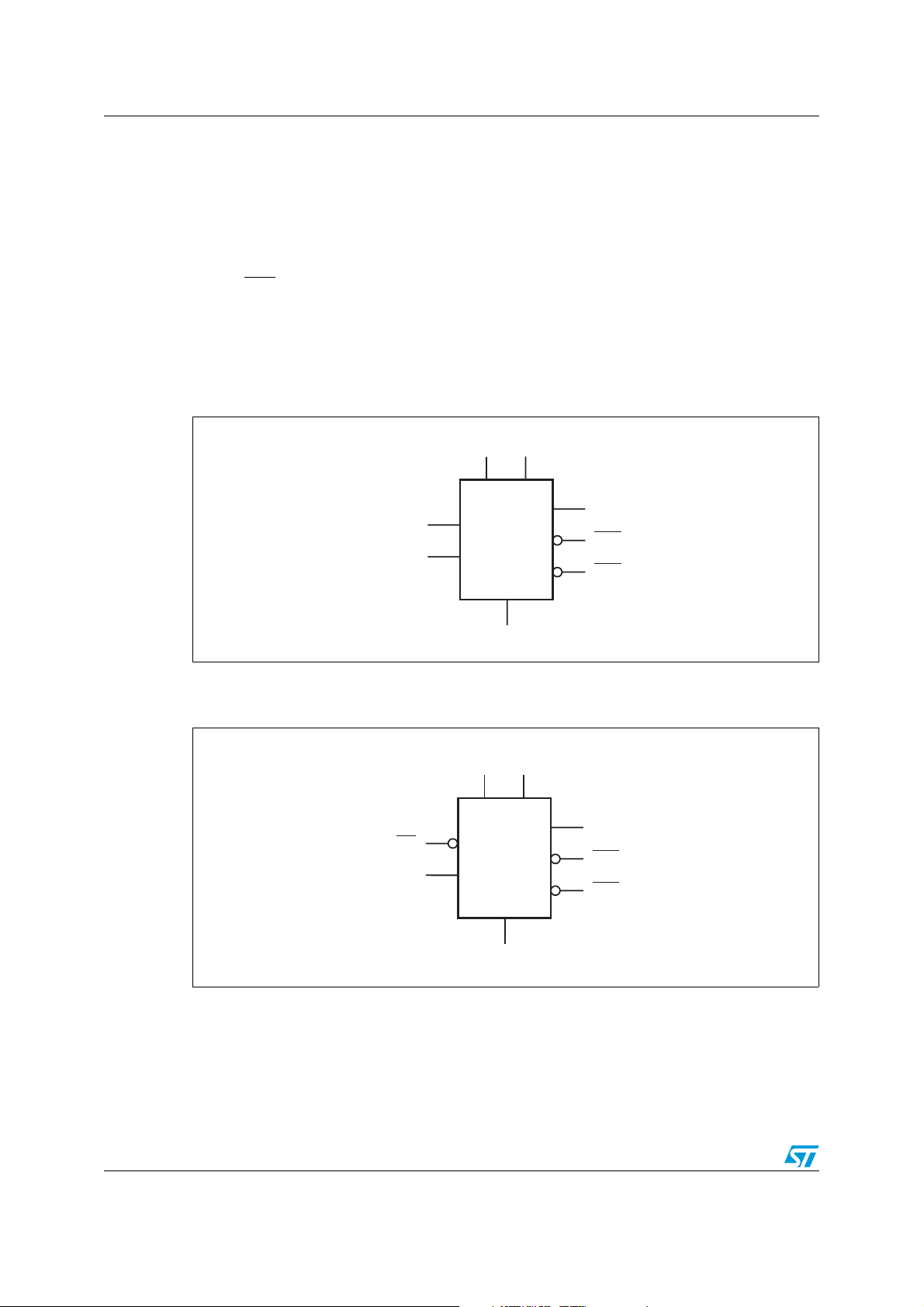
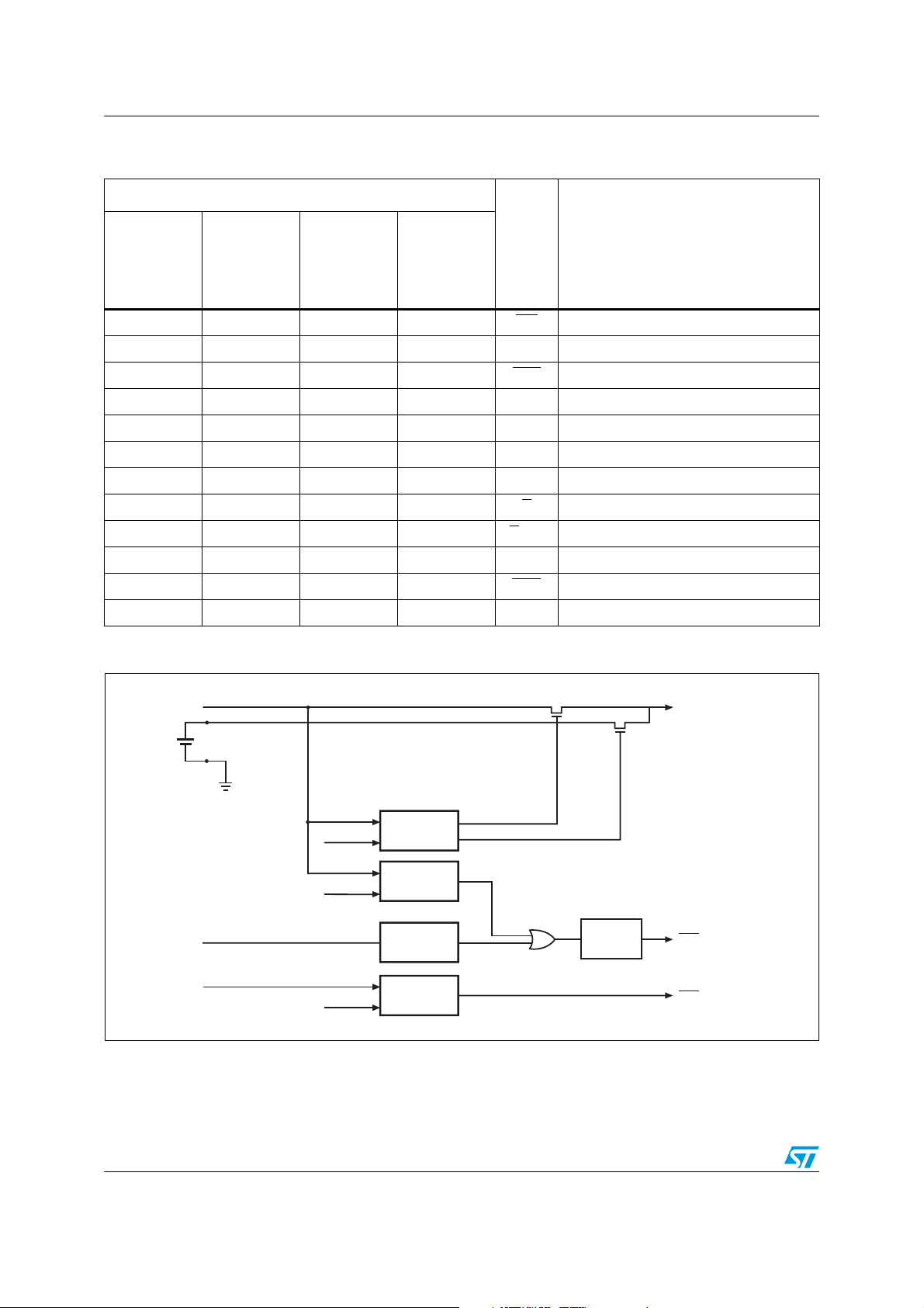
Figure 1. Logic diagram (STM690A/692/802/805/817)
VCCV
BAT
WDI
PFI
STM690A/
692A/802/
805/817
condition occurs, the reset
CC
V
OUT
RST(RST)
PFO
(1)
V
SS
1. For STM805, reset output is active-high.
Figure 2. Logic diagram (STM703/704/819)
VCCV
MR
PFI
STM703/
704/819
V
SS
BAT
V
OUT
RST
PFO
AI07894
AI07895
6/43 Doc ID 10522 Rev 10
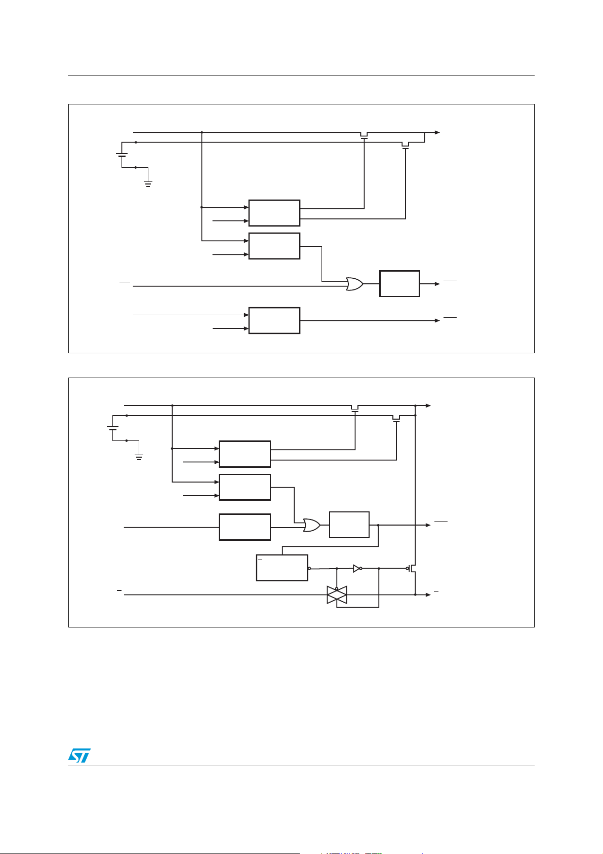
STM690A/692A/703/704/802/805/817/818/819 Description
Figure 3. Logic diagram (STM818)
VCCV
BAT
V
WDI
STM818
E
V
SS
OUT
RST
E
CON
AI07896
Table 2. Signal names
MR Push-button reset input
WDI Watchdog input
RST
Active-low reset output
RST Active-high reset outpu
(1)
E
E
CON
V
OUT
V
V
(1)
CC
BAT
Chip-enable input
Conditioned chip-enable output
Supply voltage output
Supply voltage
Backup supply voltage
PFI Power-fail input
PFO Power-fail output
Ground
1. STM818
V
SS
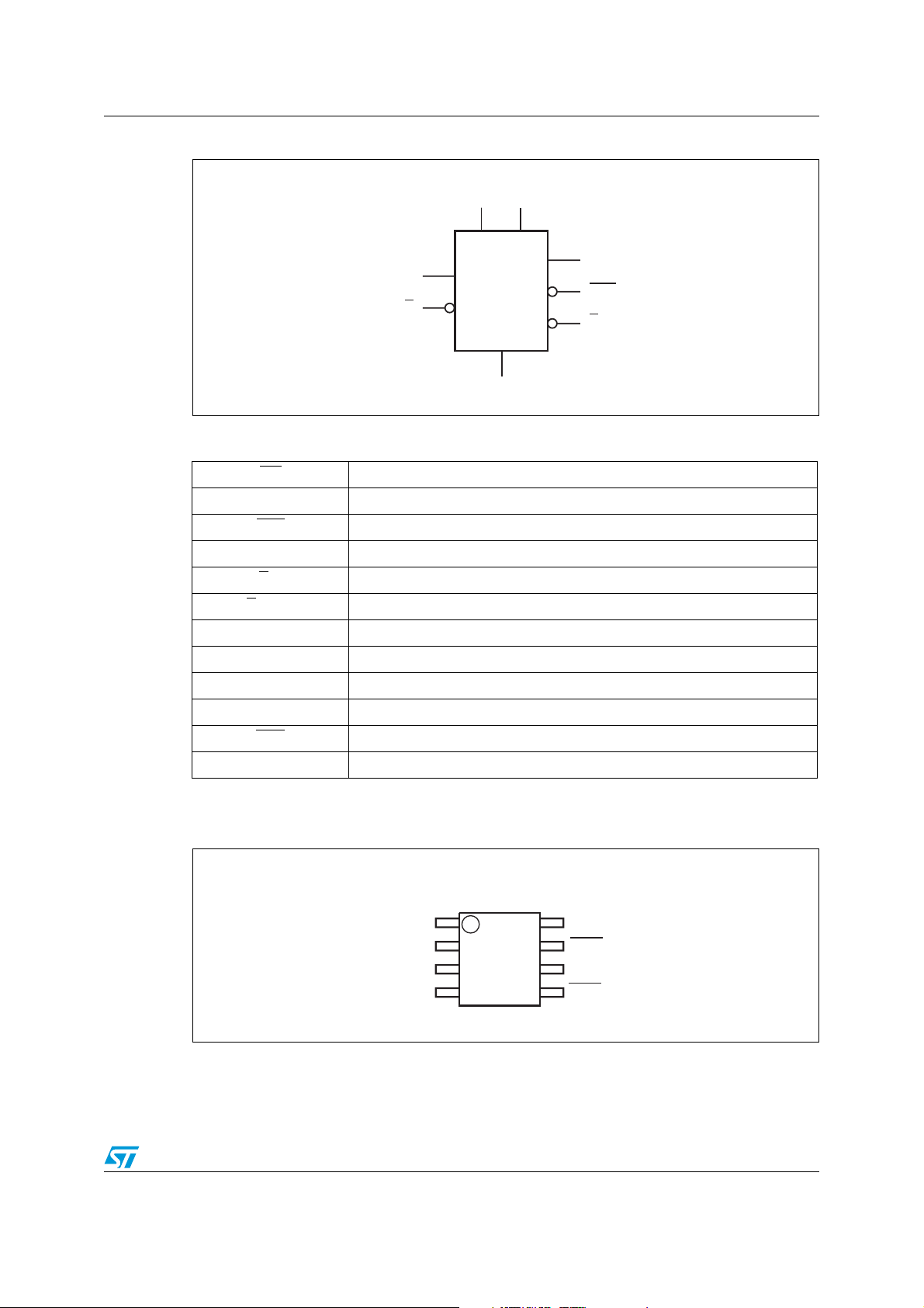
Figure 4. STM690A/692A/802/805/817 connections
SO8/TSSOP8
V
OUT
V
CC
V
SS
PFI
1
2
3
4
8
7
6
5
V
BAT
RST(RST)
WDI
PFO
(1)
AI07889
1. For STM805, reset output is active-high.
Doc ID 10522 Rev 10 7/43
Description STM690A/692A/703/704/802/805/817/818/819
Figure 5. STM703/704/819 connections
SO8/TSSOP8
V
OUT
V
CC
V
PFI
SS
1
2
3
4
V
BAT
8
RST
7
MR
6
PFO
5
AI07890
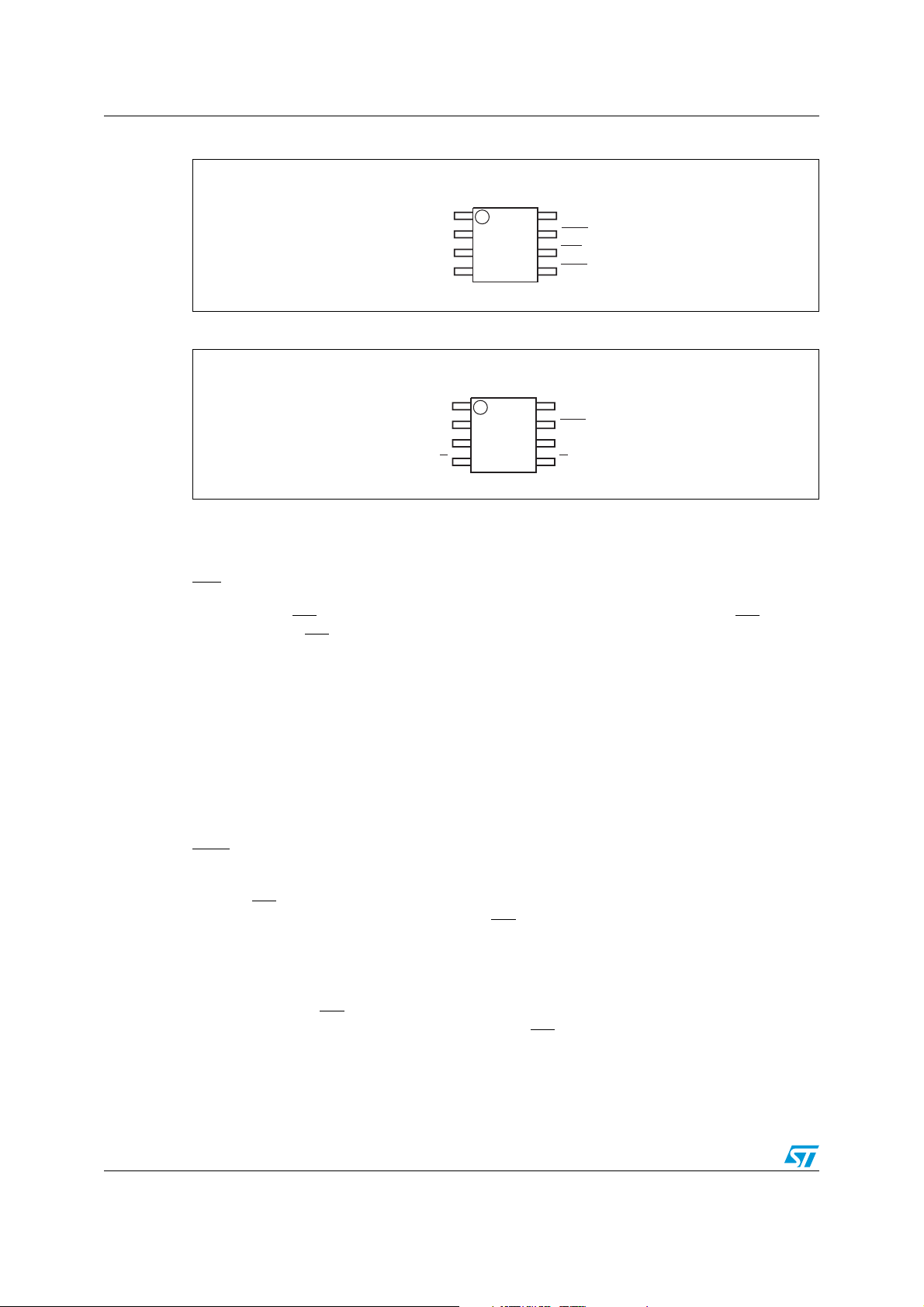
Figure 6. STM818 connections
SO8/TSSOP8
V
OUT
V
V
CC
SS
1
2
3
E
4
V
BAT
8
7
RST
WDI
6
E
5
CON
AI07892
1.1 Pin descriptions
1.1.1 MR
A logic low on MR asserts the reset output. Reset remains asserted as long as MR is low
and for t
driven from a TTL or CMOS logic line, or shorted to ground with a switch. Leave open if
unused.
1.1.2 WDI
If WDI remains high or low for 1.6 sec, the internal watchdog timer runs out and reset is
triggered. The internal watchdog timer clears while reset is asserted or when WDI sees a
rising or falling edge.
The watchdog function can be disabled by allowing the WDI pin to float.
1.1.3 RST
Pulses low for t
or when MR
threshold, the watchdog triggers a reset, or MR
1.1.4 RST
Pulses high for t
threshold or when MR
reset threshold, the watchdog triggers a reset, or MR
after MR returns high. This active-low input has an internal pull-up. It can be
rec
when triggered, and stays low whenever V
rec
is a logic low. It remains low for t
after either V
rec
is below the reset threshold
CC
rises above the reset
CC
goes from low to high.
when triggered, and stays high whenever VCC is above the reset
rec
is a logic high. It remains high for t
after either VCC falls below the
rec
goes from high to low.
8/43 Doc ID 10522 Rev 10

STM690A/692A/703/704/802/805/817/818/819 Description
1.1.5 V
OUT
When VCC is above the switchover voltage (VSO), V
channel MOSFET switch. When V
1.1.6 V
BAT
When VCC falls below VSO, V
hysteresis, V
used.
1.1.7 E
The input to the chip-enable gating circuit. Connect to ground if unused.
1.1.8 E
E
CON
CON
asserted, E
disabled mode, E
1.1.9 PFI
When PFI is less than V
otherwise, PFO
is connected to VCC through a P-
OUT reconnects to V
OUT
falls below VSO, V
CC
switches from V
. V
CC
may exceed VCC. Connect to V
BAT
CC
OUT
to V
connects to V
BAT
. When V
BAT
goes low only when E is low and reset is not asserted. If E
will remain low for 15 µs or until E goes high, whichever occurs first. In the
CON
is pulled up to V
CON
PFI
.
OUT
or when VCC falls below 2.4 V (or VSO), PFO goes low;
remains high. Connect to ground if unused.
.
OUT
rises above V
CC
is low when reset is
CON
if no battery is
CC
SO
+
1.1.10 PFO
When PFI is less than V
PFO
remains high. Leave open if unused. Output type is push-pull.
, or VCC falls below 2.4 V (or VSO), PFO goes low; otherwise,
PFI
Doc ID 10522 Rev 10 9/43
Description STM690A/692A/703/704/802/805/817/818/819
Table 3. Pin description
Pin
STM690A
STM818
STM692A
STM802
STM817
--6-MR
STM703
STM704
STM819
Name Function
STM805
Push-button reset input
6 6 - 6 WDI Watchdog input
777 -RSTActive-low reset output
- - - 7 RST Active-high reset output
1111V
2222V
8888V
4-- -E
5-- -E
Supply output for external LPSRAM
OUT
Supply voltage
CC
Backup battery input
BAT
Chip-enable input
Conditioned chip-enable output
CON
- 4 4 4 PFI Power-fail input
-555PFOPower-fail output (push-pull)
3333V
SS
Ground
Figure 7. Block diagram (STM690A/692A/802/805/817)
V
CC
V
BAT
WDI
PFI
1. For STM805, reset output is active-high.
V
OUT
V
SO
V
RST
V
PFI
COMPARE
COMPARE
WATCHDOG
TIMER
COMPARE
t
rec
Generator
RST(RST)
PFO
(1)
AI07897
10/43 Doc ID 10522 Rev 10
STM690A/692A/703/704/802/805/817/818/819 Description
Figure 8. Block diagram (STM703/704/819)
V
CC
V
BAT
V
SO
V
RST
MR
PFI
V
PFI
Figure 9. Block diagram (STM818)
V
CC
COMPARE
COMPARE
COMPARE
t
rec
Generator
V
OUT
RST
PFO
AI07898
V
OUT
WDI
V
BAT
V
SO
V
RST
E
COMPARE
COMPARE
WATCHDOG
TIMER
E
OUTPUT
CON
CONTROL
t
rec
Generator
RST
E
CON
AI07899a
Doc ID 10522 Rev 10 11/43
Description STM690A/692A/703/704/802/805/817/818/819
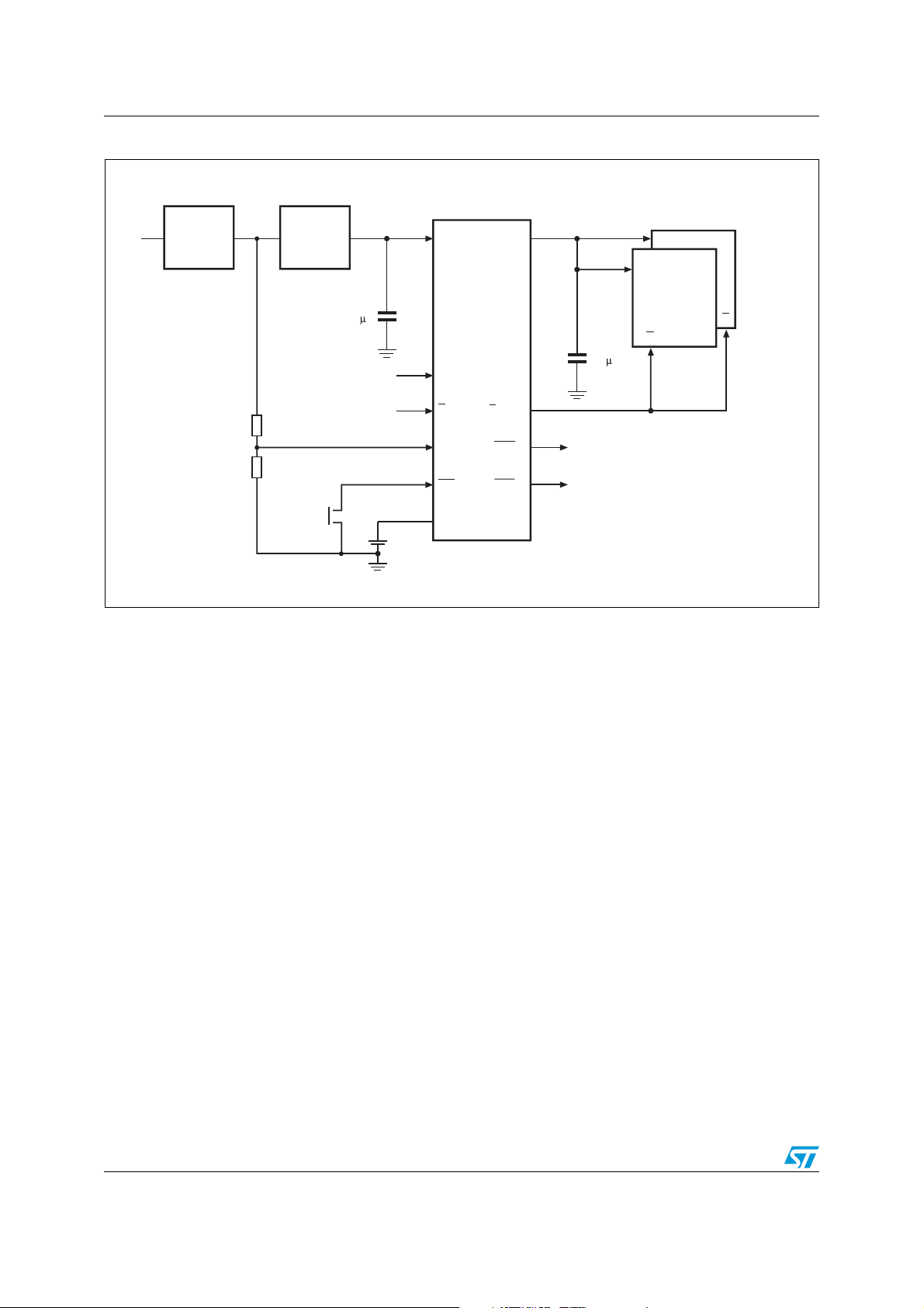
Figure 10. Hardware hookup
Unregulated
Voltage
Regulator
V
IN
From Microprocessor
R1
R2
1. For STM690A/692A/802/805/817/818.
2. For STM818 only.
3. Not available on STM818.
4. For STM703/704/819.
5. Active high on STM805.
V
CC
0.1
Push-Button
V
CC
LPSRAM
V
CC
E
V
CC
V
OUT
STM690A/692A/
F
703/704/802/805/
817/818/819
E
0.1 F
(1)
WDI
E
PFI
MR
V
(2)
(3)
(4)
BAT
(2)
E
CON
(3)
PFO
(5)
RST To Microprocessor Reset
To Microprocessor NMI
AI07893
12/43 Doc ID 10522 Rev 10

STM690A/692A/703/704/802/805/817/818/819 Operation
2 Operation
2.1 Reset output
The STM690A/692A/703/704/802/805/817/818/819 Supervisor asserts a reset signal to the
MCU whenever V
when the Push-button Reset Input (MR
(logic high for STM805) for 0V < V
battery, RST
is guaranteed valid down to VCC =1 V.
goes below the reset threshold (V
CC
) is taken low. RST is guaranteed to be a logic low
CC
< V
if VBAT is greater than 1 V. Without a backup
RST
, a watchdog time-out occurs, or
RST)
During power-up, once V
the reset time-out period, t
If V
drops below the reset threshold, RST goes low. Each time RST is asserted, it stays
CC
low for at least the reset time-out period (t
the internal timer clears. The reset timer starts when V
exceeds the reset threshold an internal timer keeps RST low for
CC
. After this interval RST returns high.
rec
). Any time VCC goes below the reset threshold
rec
returns above the reset threshold.
CC
2.2 Push-button reset input (STM703/704/819)
A logic low on MR asserts reset. Reset remains asserted while MR is low, and for t
Figure 41) after it returns high. The MR
input has an internal 40 kΩ pull-up resistor, allowing
it to be left open if not used. This input can be driven with TTL/CMOS-logic levels or with
open-drain/collector outputs. Connect a normally open momentary switch from MR
to create a manual reset function; external debounce circuitry is not required. If MR
from long cables or the device is used in a noisy environment, connect a 0.1 µF capacitor
from MR
to GND to provide additional noise immunity. MR may float, or be tied to VCC when
not used.
2.3 Watchdog input (NOT available on STM703/704/819)
The watchdog timer can be used to detect an out-of-control MCU. If the MCU does not
toggle the Watchdog Input (WDI) within t
watchdog timer is cleared by either:
1. a reset pulse, or
2. by toggling WDI (high-to-low or low-to-high), which can detect pulses as short as 50ns.
If WDI is tied high or low, a reset pulse is triggered every 1.8 sec (t
The timer remains cleared and does not count for as long as reset is asserted. As soon as
reset is released, the timer starts counting (see Figure 42).
(1.6 sec typ), the reset is asserted. The internal
WD
+ t
WD
rec
).
(see
rec
to GND
is driven
Note: 1 The watchdog function may be disabled by floating WDI or tri-stating the driver connected to
WDI. When tri-stated or disconnected, the maximum allowable leakage current is 10 µA and
the maximum allowable load capacitance is 200 pF.
2 Input pulses less than 20 ns will be ignored.
Doc ID 10522 Rev 10 13/43
 Loading...