

STM690A, STM692A, STM703
STM704, STM802, STM805, STM817/8/9
5 V supervisor with battery switchover
Features
■ 5 V operating voltage
■ NVRAM supervisor for external LPSRAM
■ Chip-enable gating (STM818 only) for external
LPSRAM (7 ns max prop delay)
■ RST and RST outputs
■ 200 ms (typ) t
■
Watchdog timer - 1.6 sec (typ)
■ Automatic battery switchover
■ Low battery supply current - 0.4 µA (typ)
■ Power-fail comparator (PFI/PFO)
■ Low supply current - 40 µA (typ)
■ Guaranteed RST (RST) assertion down to
V
= 1.0 V
CC
■ Operating temperature:
–40 °C to +85 °C (industrial grade)
■ RoHS compliance
– Lead-free components are compliant with
the RoHS directive
rec
8
1
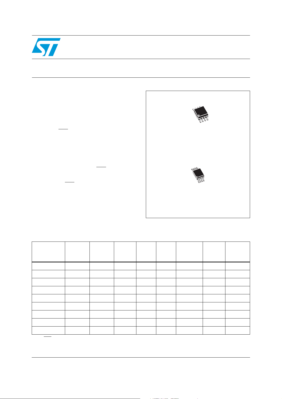
SO8 (M)
TSSOP8 3 x 3 (DS)
1. Contact local ST sales office for availability.
(1)
Table 1. Device summary
(1)
Battery
switch-
over
Power-fail
comparator
Chip-
enable
gating
Battery
freshness
seal
www.st.com
1
Manual
reset
input
Part number
STM690A ✓✓ ✓✓
STM692A ✓✓ ✓✓
STM703 ✓✓✓✓
STM704 ✓✓✓✓
STM802L/M ✓✓ ✓✓
STM805L ✓✓✓✓
STM817L/M ✓✓ ✓✓ ✓
STM818L/M ✓✓ ✓ ✓✓
STM819L/M ✓✓✓✓ ✓
1. All RST and RST outputs are push-pull.
August 2010 Doc ID 10522 Rev 10 1/43
Watchdog
input
Active-low
RST
(1)
Active-
high RST

Contents STM690A/692A/703/704/802/805/817/818/819
Contents
1 Description . . . . . . . . . . . . . . . . . . . . . . . . . . . . . . . . . . . . . . . . . . . . . . . . . 6
1.1 Pin descriptions . . . . . . . . . . . . . . . . . . . . . . . . . . . . . . . . . . . . . . . . . . . . . 8
1.1.1 MR . . . . . . . . . . . . . . . . . . . . . . . . . . . . . . . . . . . . . . . . . . . . . . . . . . . . . . 8
1.1.2 WDI . . . . . . . . . . . . . . . . . . . . . . . . . . . . . . . . . . . . . . . . . . . . . . . . . . . . . 8
1.1.3 RST
1.1.4 RST . . . . . . . . . . . . . . . . . . . . . . . . . . . . . . . . . . . . . . . . . . . . . . . . . . . . . 8
. . . . . . . . . . . . . . . . . . . . . . . . . . . . . . . . . . . . . . . . . . . . . . . . . . . . . 8
1.1.5 V
1.1.6 V
1.1.7 E . . . . . . . . . . . . . . . . . . . . . . . . . . . . . . . . . . . . . . . . . . . . . . . . . . . . . . . 9
1.1.8 E
1.1.9 PFI . . . . . . . . . . . . . . . . . . . . . . . . . . . . . . . . . . . . . . . . . . . . . . . . . . . . . . 9
1.1.10 PFO
OUT . . . . . . . . . . . . . . . . . . . . . . . . . . . . . . . . . . . . . . . . . . . . . . . . . . . . . . . . . . . . . . . . . . 9
BAT . . . . . . . . . . . . . . . . . . . . . . . . . . . . . . . . . . . . . . . . . . . . . . . . . . . . . . . . . . . . . . . . . . . 9
CON . . . . . . . . . . . . . . . . . . . . . . . . . . . . . . . . . . . . . . . . . . . . . . . . . . . . . . . . . . . . . . . . . . 9
. . . . . . . . . . . . . . . . . . . . . . . . . . . . . . . . . . . . . . . . . . . . . . . . . . . . . 9
2 Operation . . . . . . . . . . . . . . . . . . . . . . . . . . . . . . . . . . . . . . . . . . . . . . . . . 13
2.1 Reset output . . . . . . . . . . . . . . . . . . . . . . . . . . . . . . . . . . . . . . . . . . . . . . . 13
2.2 Push-button reset input (STM703/704/819) . . . . . . . . . . . . . . . . . . . . . . . 13
2.3 Watchdog input (NOT available on STM703/704/819) . . . . . . . . . . . . . . . 13
2.4 Backup battery switchover . . . . . . . . . . . . . . . . . . . . . . . . . . . . . . . . . . . . 14
2.5 Chip-enable gating (STM818 only) . . . . . . . . . . . . . . . . . . . . . . . . . . . . . . 15
2.6 Chip-enable input (STM818 only) . . . . . . . . . . . . . . . . . . . . . . . . . . . . . . . 15
2.7 Chip-enable output (STM818 only) . . . . . . . . . . . . . . . . . . . . . . . . . . . . . 15
2.8 Power-fail input/output (NOT available on STM818) . . . . . . . . . . . . . . . . 16
2.9 Applications information . . . . . . . . . . . . . . . . . . . . . . . . . . . . . . . . . . . . . . 16
2.10 Using a SuperCap™ as a backup power source . . . . . . . . . . . . . . . . . . . 17
2.11 Negative-going V
transients . . . . . . . . . . . . . . . . . . . . . . . . . . . . . . . . . 18
CC
2.12 Battery freshness seal (STM817/818/819) . . . . . . . . . . . . . . . . . . . . . . . . 19
3 Typical operating characteristics . . . . . . . . . . . . . . . . . . . . . . . . . . . . . 20
4 Maximum ratings . . . . . . . . . . . . . . . . . . . . . . . . . . . . . . . . . . . . . . . . . . . 31
5 DC and AC parameters . . . . . . . . . . . . . . . . . . . . . . . . . . . . . . . . . . . . . . 32
2/43 Doc ID 10522 Rev 10

STM690A/692A/703/704/802/805/817/818/819 Contents
6 Package mechanical data . . . . . . . . . . . . . . . . . . . . . . . . . . . . . . . . . . . . 37
7 Part numbering . . . . . . . . . . . . . . . . . . . . . . . . . . . . . . . . . . . . . . . . . . . . 40
8 Revision history . . . . . . . . . . . . . . . . . . . . . . . . . . . . . . . . . . . . . . . . . . . 42
Doc ID 10522 Rev 10 3/43

List of tables STM690A/692A/703/704/802/805/817/818/819
List of tables
Table 1. Device summary . . . . . . . . . . . . . . . . . . . . . . . . . . . . . . . . . . . . . . . . . . . . . . . . . . . . . . . . . . 1
Table 2. Signal names . . . . . . . . . . . . . . . . . . . . . . . . . . . . . . . . . . . . . . . . . . . . . . . . . . . . . . . . . . . . 7
Table 3. Pin description . . . . . . . . . . . . . . . . . . . . . . . . . . . . . . . . . . . . . . . . . . . . . . . . . . . . . . . . . . 10
Table 4. I/O status in battery backup . . . . . . . . . . . . . . . . . . . . . . . . . . . . . . . . . . . . . . . . . . . . . . . . 14
Table 5. Absolute maximum ratings . . . . . . . . . . . . . . . . . . . . . . . . . . . . . . . . . . . . . . . . . . . . . . . . . 31
Table 6. Operating and AC measurement conditions. . . . . . . . . . . . . . . . . . . . . . . . . . . . . . . . . . . . 32
Table 7. DC and AC characteristics . . . . . . . . . . . . . . . . . . . . . . . . . . . . . . . . . . . . . . . . . . . . . . . . . 34
Table 8. SO8 - 8-lead plastic small outline, 150 mils body width, package mechanical data . . . . . . 38
Table 9. TSSOP8 - 8-lead, thin shrink small outline, 3 x 3 mm body size, mechanical data . . . . . . 39
Table 10. Ordering information scheme . . . . . . . . . . . . . . . . . . . . . . . . . . . . . . . . . . . . . . . . . . . . . . . 40
Table 11. Marking description. . . . . . . . . . . . . . . . . . . . . . . . . . . . . . . . . . . . . . . . . . . . . . . . . . . . . . . 41
Table 12. Document revision history . . . . . . . . . . . . . . . . . . . . . . . . . . . . . . . . . . . . . . . . . . . . . . . . . 42
4/43 Doc ID 10522 Rev 10

STM690A/692A/703/704/802/805/817/818/819 List of figures
List of figures
Figure 1. Logic diagram (STM690A/692/802/805/817) . . . . . . . . . . . . . . . . . . . . . . . . . . . . . . . . . . . . 6
Figure 2. Logic diagram (STM703/704/819) . . . . . . . . . . . . . . . . . . . . . . . . . . . . . . . . . . . . . . . . . . . . 6
Figure 3. Logic diagram (STM818) . . . . . . . . . . . . . . . . . . . . . . . . . . . . . . . . . . . . . . . . . . . . . . . . . . . 7
Figure 4. STM690A/692A/802/805/817 connections . . . . . . . . . . . . . . . . . . . . . . . . . . . . . . . . . . . . . . 7
Figure 5. STM703/704/819 connections . . . . . . . . . . . . . . . . . . . . . . . . . . . . . . . . . . . . . . . . . . . . . . . 8
Figure 6. STM818 connections . . . . . . . . . . . . . . . . . . . . . . . . . . . . . . . . . . . . . . . . . . . . . . . . . . . . . . 8
Figure 7. Block diagram (STM690A/692A/802/805/817) . . . . . . . . . . . . . . . . . . . . . . . . . . . . . . . . . . 10
Figure 8. Block diagram (STM703/704/819) . . . . . . . . . . . . . . . . . . . . . . . . . . . . . . . . . . . . . . . . . . . 11
Figure 9. Block diagram (STM818) . . . . . . . . . . . . . . . . . . . . . . . . . . . . . . . . . . . . . . . . . . . . . . . . . . 11
Figure 10. Hardware hookup . . . . . . . . . . . . . . . . . . . . . . . . . . . . . . . . . . . . . . . . . . . . . . . . . . . . . . . . 12
Figure 11. Chip-enable gating . . . . . . . . . . . . . . . . . . . . . . . . . . . . . . . . . . . . . . . . . . . . . . . . . . . . . . . 15
Figure 12. Chip-enable waveform . . . . . . . . . . . . . . . . . . . . . . . . . . . . . . . . . . . . . . . . . . . . . . . . . . . . 16
Figure 13. Power-fail comparator waveform (STM817/818/819) . . . . . . . . . . . . . . . . . . . . . . . . . . . . . 17
Figure 14. Power-fail comparator waveform (STM690A/692A/703/704/802/805) . . . . . . . . . . . . . . . . 17
Figure 15. Using a SuperCap™ . . . . . . . . . . . . . . . . . . . . . . . . . . . . . . . . . . . . . . . . . . . . . . . . . . . . . . 19
Figure 16. Freshness seal enable waveform . . . . . . . . . . . . . . . . . . . . . . . . . . . . . . . . . . . . . . . . . . . . 19
Figure 17. V
Figure 18. V
Figure 19. Supply current vs. temperature (no load) . . . . . . . . . . . . . . . . . . . . . . . . . . . . . . . . . . . . . . 21
Figure 20. Battery current vs. temperature . . . . . . . . . . . . . . . . . . . . . . . . . . . . . . . . . . . . . . . . . . . . . 21
Figure 21. V
Figure 22. Reset comparator propagation delay vs. temperature (other than STM817/818/819) . . . . 22
Figure 23. Reset comparator propagation delay vs. temperature (V
Figure 24. Power-up t
Figure 25. Normalized reset threshold vs. temperature . . . . . . . . . . . . . . . . . . . . . . . . . . . . . . . . . . . . 24
Figure 26. Watchdog time-out period vs. temperature. . . . . . . . . . . . . . . . . . . . . . . . . . . . . . . . . . . . . 24
Figure 27. E
Figure 28. PFI to PFO
Figure 29. Output voltage vs. load current (V
Figure 30. Output voltage vs. load current (V
Figure 31. RST
Figure 32. RST output voltage vs. supply voltage . . . . . . . . . . . . . . . . . . . . . . . . . . . . . . . . . . . . . . . . 27
Figure 33. RST
Figure 34. RST response time (assertion) . . . . . . . . . . . . . . . . . . . . . . . . . . . . . . . . . . . . . . . . . . . . . . 28
Figure 35. Power-fail comparator response time (assertion) . . . . . . . . . . . . . . . . . . . . . . . . . . . . . . . . 29
Figure 36.
Figure 37. Maximum transient duration vs. reset threshold overdrive . . . . . . . . . . . . . . . . . . . . . . . . . 30
Figure 38. E
Figure 39. E
Figure 40. AC testing input/output waveforms . . . . . . . . . . . . . . . . . . . . . . . . . . . . . . . . . . . . . . . . . . . 33
Figure 41. MR
Figure 42. Watchdog timing . . . . . . . . . . . . . . . . . . . . . . . . . . . . . . . . . . . . . . . . . . . . . . . . . . . . . . . . . 33
Figure 43. SO8 - 8-lead plastic small outline, 150 mils body width, package mechanical drawing . . . 38
Figure 44. TSSOP8 - 8-lead, thin shrink small outline, 3 x 3 mm body size, outline . . . . . . . . . . . . . . 39
to V
CC
to V
BAT
threshold vs. temperature . . . . . . . . . . . . . . . . . . . . . . . . . . . . . . . . . . . . . . . . . . . . . . 22
PFI
to E
CON
on-resistance vs. temperature . . . . . . . . . . . . . . . . . . . . . . . . . . . . . . . . . . . . 20
OUT
on-resistance vs. temperature . . . . . . . . . . . . . . . . . . . . . . . . . . . . . . . . . . . 20
OUT
= 3.0 V; STM817/818/819) . 23
vs. temperature . . . . . . . . . . . . . . . . . . . . . . . . . . . . . . . . . . . . . . . . . . . . . 23
REC
BAT
on-resistance vs. temperature . . . . . . . . . . . . . . . . . . . . . . . . . . . . . . . . . . . . . . 25
propagation delay vs. temperature . . . . . . . . . . . . . . . . . . . . . . . . . . . . . . . . . 25
= 5 V; V
CC
= 0 V; V
CC
= 2.8 V; TA = 25 °C) . . . . . . . . . . . . . . . 26
BAT
= 2.8 V; TA = 25 °C) . . . . . . . . . . . . . . . 26
BAT
output voltage vs. supply voltage . . . . . . . . . . . . . . . . . . . . . . . . . . . . . . . . . . . . . . . . 27
response time (assertion) . . . . . . . . . . . . . . . . . . . . . . . . . . . . . . . . . . . . . . . . . . . . . . 28
Power-fail comparator response time (de-assertion) . . . . . . . . . . . . . . . . . . . . . . . . . . . . . . . . . . . . . .29
to E
to E
propagation delay vs. temperature . . . . . . . . . . . . . . . . . . . . . . . . . . . . . . . . . . 30
CON
propagation delay test circuit . . . . . . . . . . . . . . . . . . . . . . . . . . . . . . . . . . . . . . . 32
CON
timing waveform . . . . . . . . . . . . . . . . . . . . . . . . . . . . . . . . . . . . . . . . . . . . . . . . . . . . . . 33
Doc ID 10522 Rev 10 5/43
Description STM690A/692A/703/704/802/805/817/818/819
1 Description
The STM690A/692A/703/704/802/805/817/818/819 supervisors are self-contained devices
which provide microprocessor supervisory functions with the ability to non-volatize and
write-protect external LPSRAM. A precision voltage reference and comparator monitors the
V
input for an out-of-tolerance condition. When an invalid V
CC
output (RST
) is forced low (or high in the case of RST). These devices also offer a watchdog
timer (except for STM703/704/819) as well as a power-fail comparator (except for STM818)
to provide the system with an early warning of impending power failure.
These devices are available in a standard 8-pin SOIC package or a space-saving 8-pin
TSSOP package.
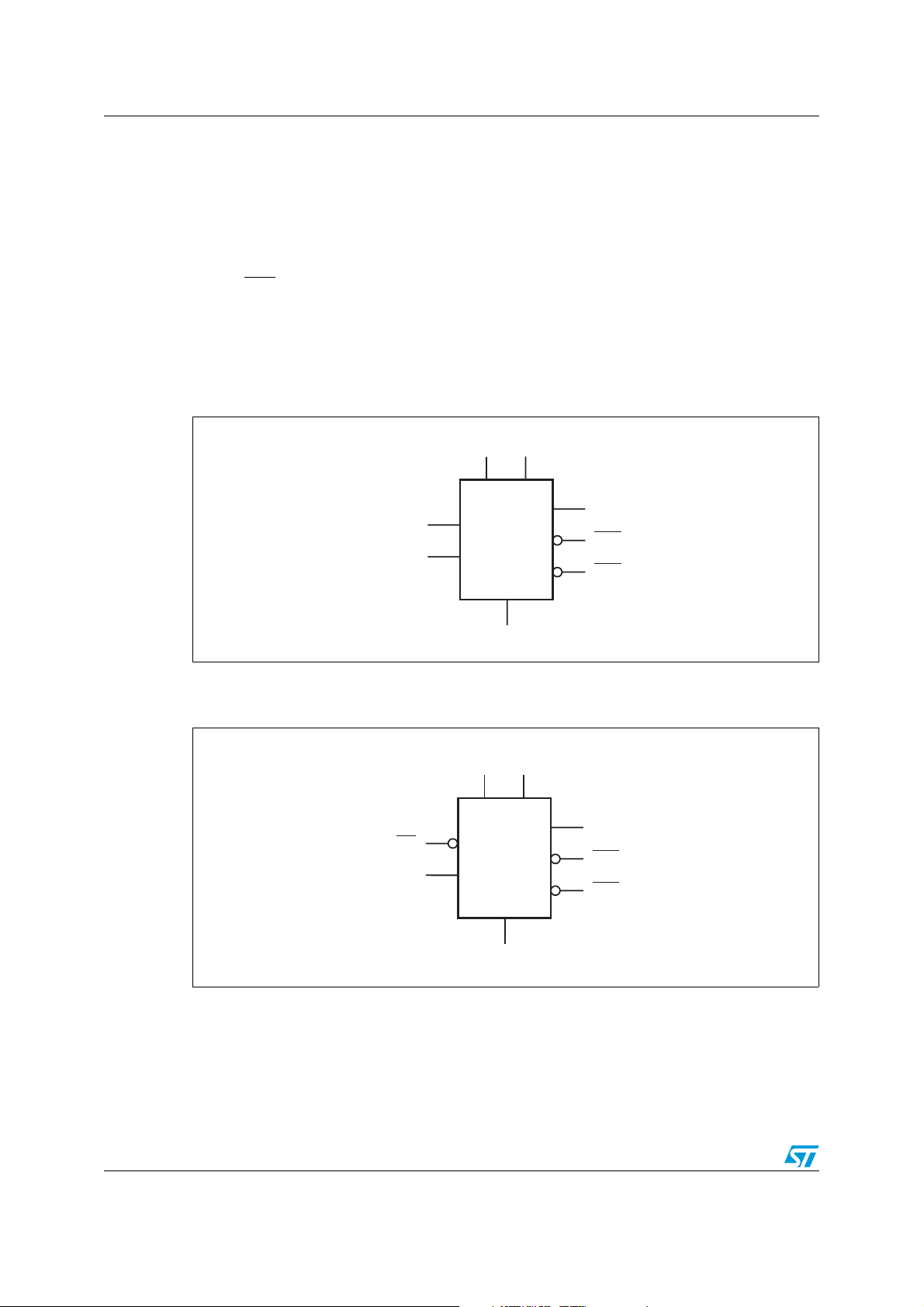
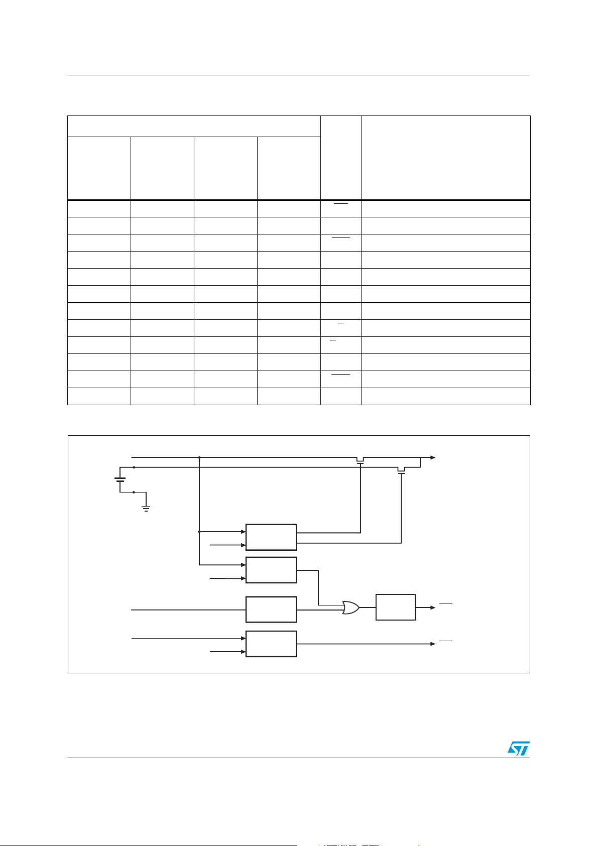
Figure 1. Logic diagram (STM690A/692/802/805/817)
VCCV
BAT
WDI
PFI
STM690A/
692A/802/
805/817
condition occurs, the reset
CC
V
OUT
RST(RST)
PFO
(1)
V
SS
1. For STM805, reset output is active-high.
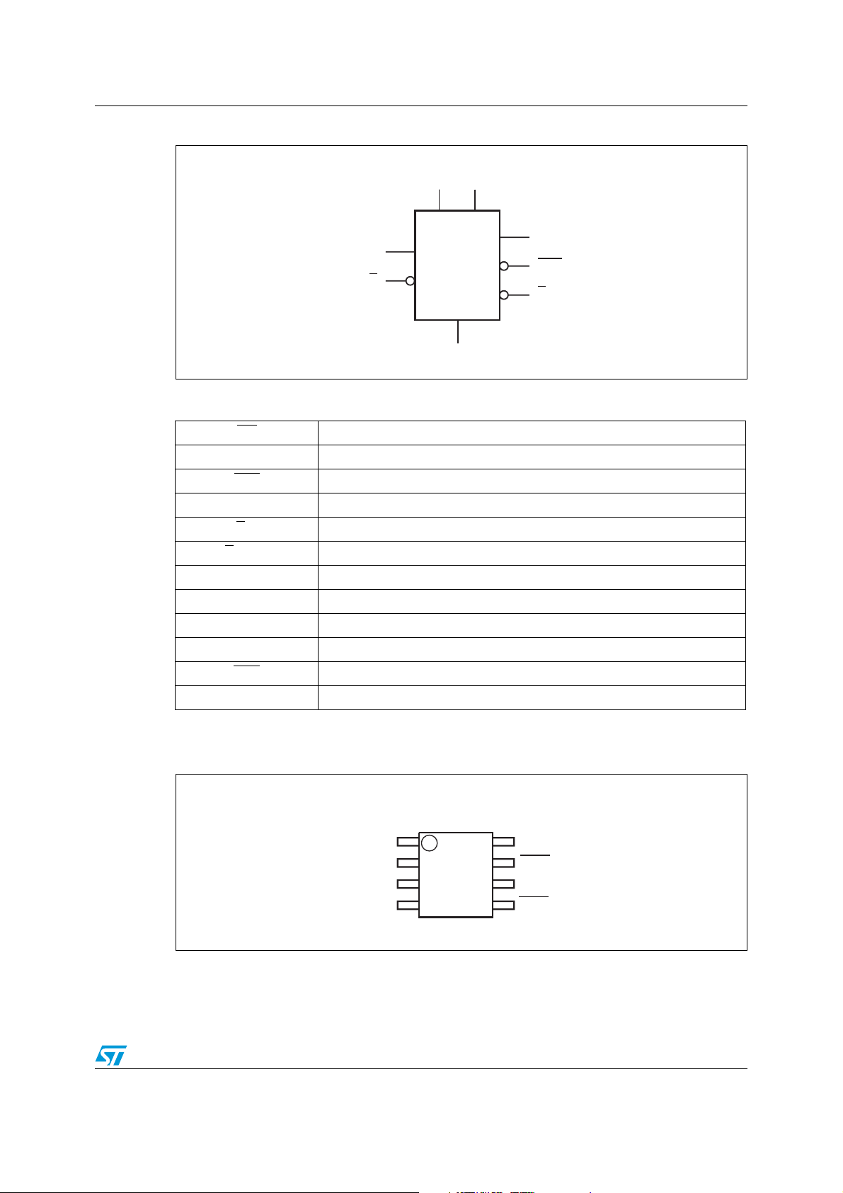
Figure 2. Logic diagram (STM703/704/819)
VCCV
MR
PFI
STM703/
704/819
V
SS
BAT
V
OUT
RST
PFO
AI07894
AI07895
6/43 Doc ID 10522 Rev 10
STM690A/692A/703/704/802/805/817/818/819 Description
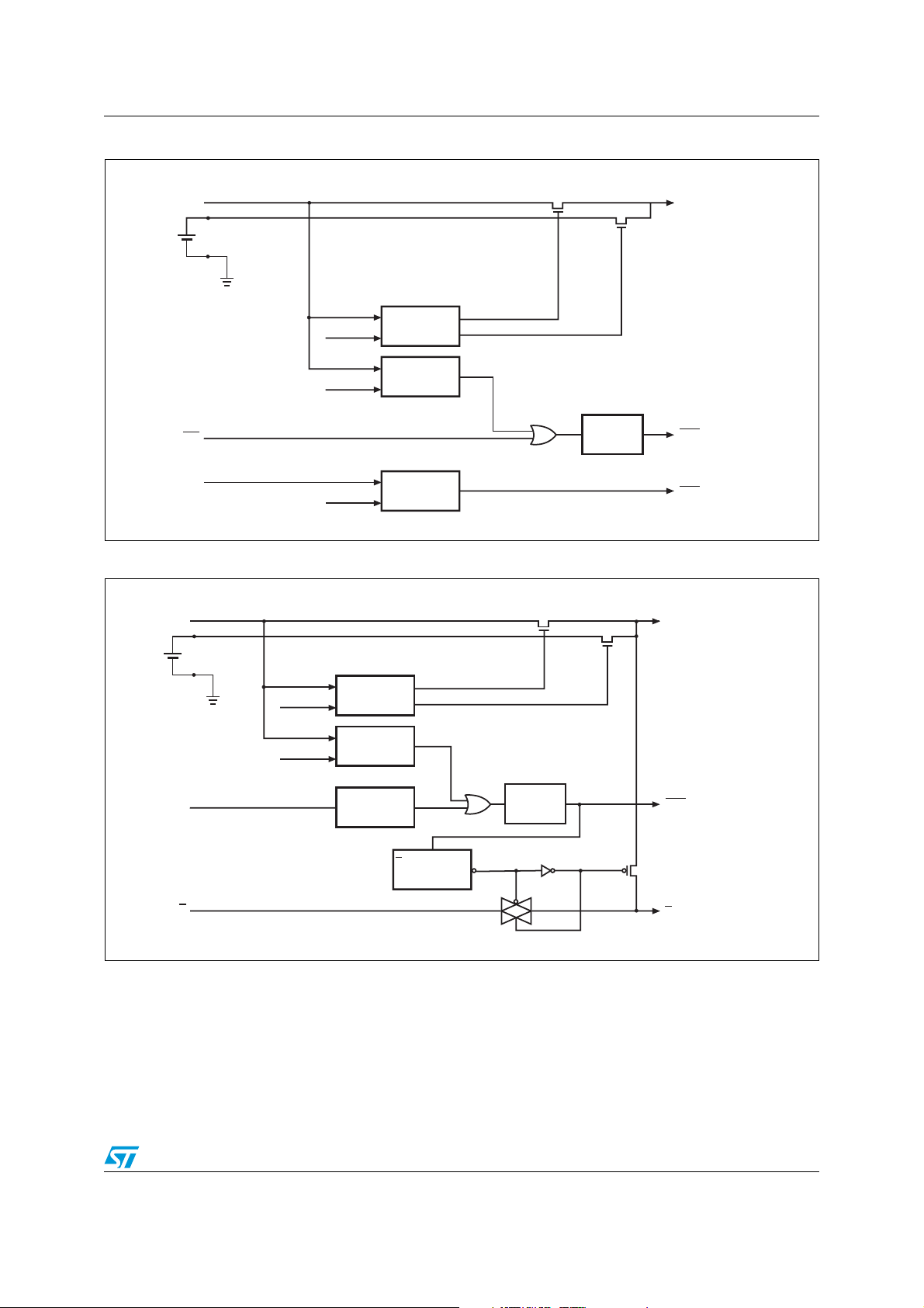
Figure 3. Logic diagram (STM818)
VCCV
BAT
V
WDI
STM818
E
V
SS
OUT
RST
E
CON
AI07896
Table 2. Signal names
MR Push-button reset input
WDI Watchdog input
RST
Active-low reset output
RST Active-high reset outpu
(1)
E
E
CON
V
OUT
V
V
(1)
CC
BAT
Chip-enable input
Conditioned chip-enable output
Supply voltage output
Supply voltage
Backup supply voltage
PFI Power-fail input
PFO Power-fail output
Ground
1. STM818
V
SS
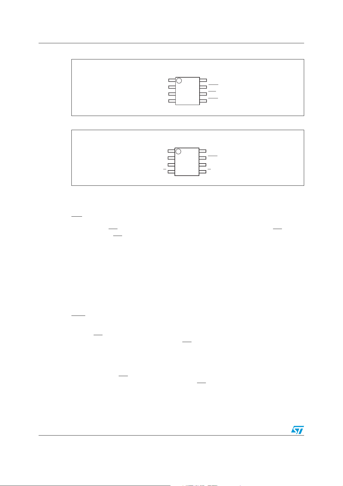
Figure 4. STM690A/692A/802/805/817 connections
SO8/TSSOP8
V
OUT
V
CC
V
SS
PFI
1
2
3
4
8
7
6
5
V
BAT
RST(RST)
WDI
PFO
(1)
AI07889
1. For STM805, reset output is active-high.
Doc ID 10522 Rev 10 7/43
Description STM690A/692A/703/704/802/805/817/818/819
Figure 5. STM703/704/819 connections
SO8/TSSOP8
V
OUT
V
CC
V
PFI
SS
1
2
3
4
V
BAT
8
RST
7
MR
6
PFO
5
AI07890
Figure 6. STM818 connections
SO8/TSSOP8
V
OUT
V
V
CC
SS
1
2
3
E
4
V
BAT
8
7
RST
WDI
6
E
5
CON
AI07892
1.1 Pin descriptions
1.1.1 MR
A logic low on MR asserts the reset output. Reset remains asserted as long as MR is low
and for t
driven from a TTL or CMOS logic line, or shorted to ground with a switch. Leave open if
unused.
1.1.2 WDI
If WDI remains high or low for 1.6 sec, the internal watchdog timer runs out and reset is
triggered. The internal watchdog timer clears while reset is asserted or when WDI sees a
rising or falling edge.
The watchdog function can be disabled by allowing the WDI pin to float.
1.1.3 RST
Pulses low for t
or when MR
threshold, the watchdog triggers a reset, or MR
1.1.4 RST
Pulses high for t
threshold or when MR
reset threshold, the watchdog triggers a reset, or MR
after MR returns high. This active-low input has an internal pull-up. It can be
rec
when triggered, and stays low whenever V
rec
is a logic low. It remains low for t
after either V
rec
is below the reset threshold
CC
rises above the reset
CC
goes from low to high.
when triggered, and stays high whenever VCC is above the reset
rec
is a logic high. It remains high for t
after either VCC falls below the
rec
goes from high to low.
8/43 Doc ID 10522 Rev 10

STM690A/692A/703/704/802/805/817/818/819 Description
1.1.5 V
OUT
When VCC is above the switchover voltage (VSO), V
channel MOSFET switch. When V
1.1.6 V
BAT
When VCC falls below VSO, V
hysteresis, V
used.
1.1.7 E
The input to the chip-enable gating circuit. Connect to ground if unused.
1.1.8 E
E
CON
CON
asserted, E
disabled mode, E
1.1.9 PFI
When PFI is less than V
otherwise, PFO
is connected to VCC through a P-
OUT reconnects to V
OUT
falls below VSO, V
CC
switches from V
. V
CC
may exceed VCC. Connect to V
BAT
CC
OUT
to V
connects to V
BAT
. When V
BAT
goes low only when E is low and reset is not asserted. If E
will remain low for 15 µs or until E goes high, whichever occurs first. In the
CON
is pulled up to V
CON
PFI
.
OUT
or when VCC falls below 2.4 V (or VSO), PFO goes low;
remains high. Connect to ground if unused.
.
OUT
rises above V
CC
is low when reset is
CON
if no battery is
CC
SO
+
1.1.10 PFO
When PFI is less than V
PFO
remains high. Leave open if unused. Output type is push-pull.
, or VCC falls below 2.4 V (or VSO), PFO goes low; otherwise,
PFI
Doc ID 10522 Rev 10 9/43
Description STM690A/692A/703/704/802/805/817/818/819
Table 3. Pin description
Pin
STM690A
STM818
STM692A
STM802
STM817
--6-MR
STM703
STM704
STM819
Name Function
STM805
Push-button reset input
6 6 - 6 WDI Watchdog input
777 -RSTActive-low reset output
- - - 7 RST Active-high reset output
1111V
2222V
8888V
4-- -E
5-- -E
Supply output for external LPSRAM
OUT
Supply voltage
CC
Backup battery input
BAT
Chip-enable input
Conditioned chip-enable output
CON
- 4 4 4 PFI Power-fail input
-555PFOPower-fail output (push-pull)
3333V
SS
Ground
Figure 7. Block diagram (STM690A/692A/802/805/817)
V
CC
V
BAT
WDI
PFI
1. For STM805, reset output is active-high.
V
OUT
V
SO
V
RST
V
PFI
COMPARE
COMPARE
WATCHDOG
TIMER
COMPARE
t
rec
Generator
RST(RST)
PFO
(1)
AI07897
10/43 Doc ID 10522 Rev 10
STM690A/692A/703/704/802/805/817/818/819 Description
Figure 8. Block diagram (STM703/704/819)
V
CC
V
BAT
V
SO
V
RST
MR
PFI
V
PFI
Figure 9. Block diagram (STM818)
V
CC
COMPARE
COMPARE
COMPARE
t
rec
Generator
V
OUT
RST
PFO
AI07898
V
OUT
WDI
V
BAT
V
SO
V
RST
E
COMPARE
COMPARE
WATCHDOG
TIMER
E
OUTPUT
CON
CONTROL
t
rec
Generator
RST
E
CON
AI07899a
Doc ID 10522 Rev 10 11/43
Description STM690A/692A/703/704/802/805/817/818/819
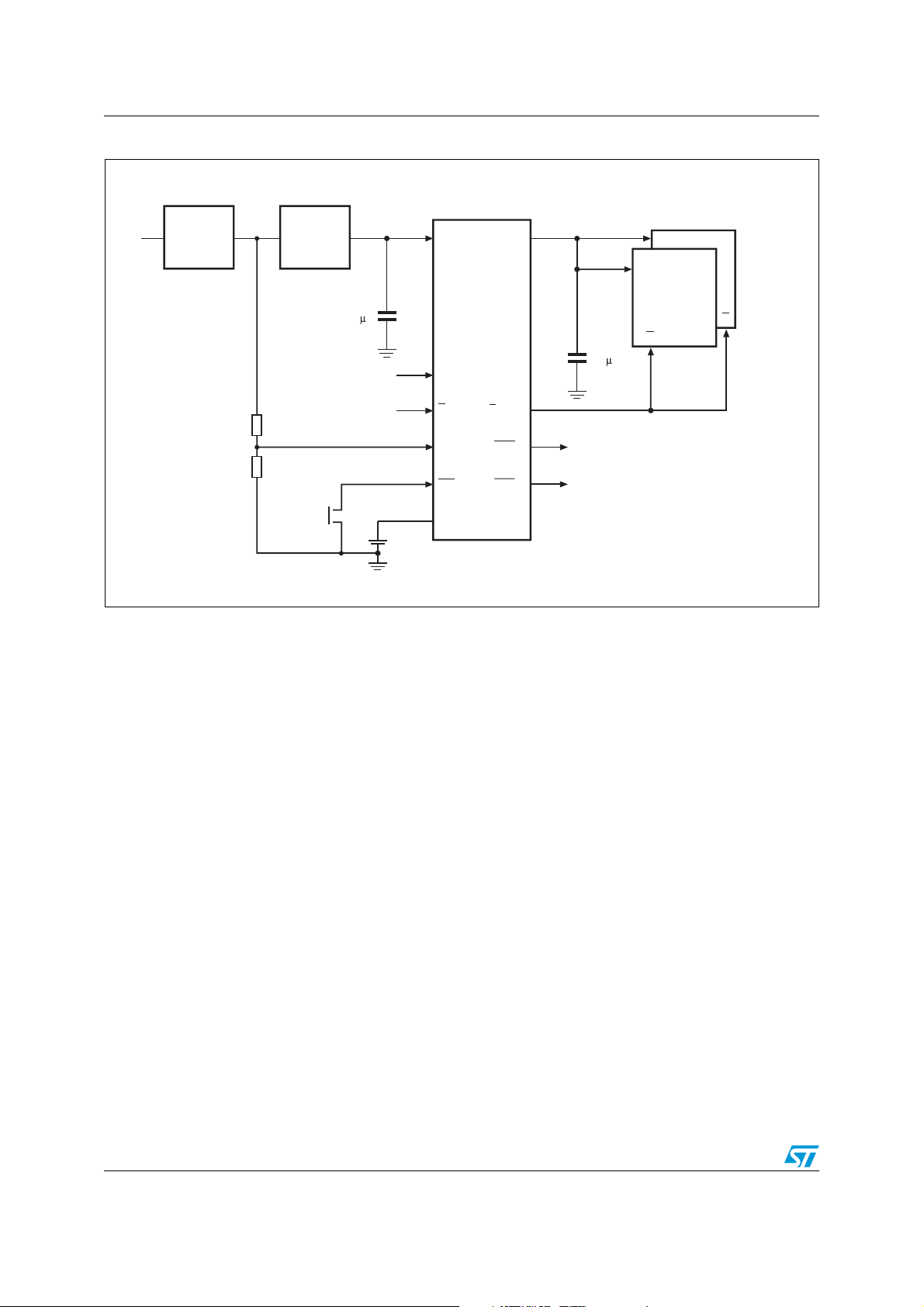
Figure 10. Hardware hookup
Unregulated
Voltage
Regulator
V
IN
From Microprocessor
R1
R2
1. For STM690A/692A/802/805/817/818.
2. For STM818 only.
3. Not available on STM818.
4. For STM703/704/819.
5. Active high on STM805.
V
CC
0.1
Push-Button
V
CC
LPSRAM
V
CC
E
V
CC
V
OUT
STM690A/692A/
F
703/704/802/805/
817/818/819
E
0.1 F
(1)
WDI
E
PFI
MR
V
(2)
(3)
(4)
BAT
(2)
E
CON
(3)
PFO
(5)
RST To Microprocessor Reset
To Microprocessor NMI
AI07893
12/43 Doc ID 10522 Rev 10

STM690A/692A/703/704/802/805/817/818/819 Operation
2 Operation
2.1 Reset output
The STM690A/692A/703/704/802/805/817/818/819 Supervisor asserts a reset signal to the
MCU whenever V
when the Push-button Reset Input (MR
(logic high for STM805) for 0V < V
battery, RST
is guaranteed valid down to VCC =1 V.
goes below the reset threshold (V
CC
) is taken low. RST is guaranteed to be a logic low
CC
< V
if VBAT is greater than 1 V. Without a backup
RST
, a watchdog time-out occurs, or
RST)
During power-up, once V
the reset time-out period, t
If V
drops below the reset threshold, RST goes low. Each time RST is asserted, it stays
CC
low for at least the reset time-out period (t
the internal timer clears. The reset timer starts when V
exceeds the reset threshold an internal timer keeps RST low for
CC
. After this interval RST returns high.
rec
). Any time VCC goes below the reset threshold
rec
returns above the reset threshold.
CC
2.2 Push-button reset input (STM703/704/819)
A logic low on MR asserts reset. Reset remains asserted while MR is low, and for t
Figure 41) after it returns high. The MR
input has an internal 40 kΩ pull-up resistor, allowing
it to be left open if not used. This input can be driven with TTL/CMOS-logic levels or with
open-drain/collector outputs. Connect a normally open momentary switch from MR
to create a manual reset function; external debounce circuitry is not required. If MR
from long cables or the device is used in a noisy environment, connect a 0.1 µF capacitor
from MR
to GND to provide additional noise immunity. MR may float, or be tied to VCC when
not used.
2.3 Watchdog input (NOT available on STM703/704/819)
The watchdog timer can be used to detect an out-of-control MCU. If the MCU does not
toggle the Watchdog Input (WDI) within t
watchdog timer is cleared by either:
1. a reset pulse, or
2. by toggling WDI (high-to-low or low-to-high), which can detect pulses as short as 50ns.
If WDI is tied high or low, a reset pulse is triggered every 1.8 sec (t
The timer remains cleared and does not count for as long as reset is asserted. As soon as
reset is released, the timer starts counting (see Figure 42).
(1.6 sec typ), the reset is asserted. The internal
WD
+ t
WD
rec
).
(see
rec
to GND
is driven
Note: 1 The watchdog function may be disabled by floating WDI or tri-stating the driver connected to
WDI. When tri-stated or disconnected, the maximum allowable leakage current is 10 µA and
the maximum allowable load capacitance is 200 pF.
2 Input pulses less than 20 ns will be ignored.
Doc ID 10522 Rev 10 13/43

Operation STM690A/692A/703/704/802/805/817/818/819
2.4 Backup battery switchover
In the event of a power failure, it may be necessary to preserve the contents of external
SRAM through V
automatically switch the SRAM to the backup supply when V
Note: When the battery is first connected without V
immediately provide backup battery voltage on V
switchover operate as described below. This mode allows a battery to be attached during
manufacturing but not used until after the system has been activated for the first time. As a
result, no battery power is consumed by the device during storage and shipment. For the
STM81x devices, the battery freshness seal can be initiated again by following the
procedure outlined in Section 2.12. If the backup battery is not used, connect both V
V
to V
OUT
Whenever V
CC
.
CC
100 Ω switch. V
be powered by V
battery life.
. With a backup battery installed with voltage V
OUT
power applied, the device does not
CC
falls below the switchover voltage, VSO, V
is the lesser of V
SO
for as long as possible before switching over thereby maximizing the
CC
BAT
and V
RST
. Only after VCC exceeds V
OUT
OUT
. Choosing the lesser allows the device to
falls.
CC
is connected to V
, the devices
BAT
will the
RST
through a
BAT
BAT
and
Assuming V
before V
OUT
external SRAMs. When V
point. V
OUT
> 2.0 V, switchover at VSO ensures that battery backup mode is entered
BAT
gets too close to the 2.0 V minimum required to reliably retain data in most
recovers, hysteresis is used to avoid oscillation around the VSO
CC
is connected to VCC through a 3 Ω PMOS power switch.
Note: The backup battery may be removed while V
decoupled (0.1 µF typ), without danger of triggering a reset.
Table 4. I/O status in battery backup
V
OUT
V
CC
PFI Disabled
PFO
E
E
CON
WDI Watchdog timer is disabled
MR
RST
RST Logic high
V
BAT
Connected to V
Disconnected from V
Logic low
High impedance
Logic high
Disabled
Logic low
Connected to V
through internal switch
BAT
OUT
OUT
is valid, assuming V
CC
is adequately
BAT
14/43 Doc ID 10522 Rev 10

STM690A/692A/703/704/802/805/817/818/819 Operation
2.5 Chip-enable gating (STM818 only)
Internal gating of the chip-enable (E) signal prevents erroneous data from corrupting the
external CMOS RAM in the event of an undervoltage condition. The STM818 uses a series
transmission gate from E
asserted), the E
transmission gate is enabled and passes all E transitions. When reset is
to E
(see Figure 11). During normal operation (reset not
CON
asserted, this path becomes disabled, preventing erroneous data from corrupting the CMOS
RAM. The short propagation delay from E
most µPs. If E
is low when reset asserts, E
goes high) to permit the current WRITE cycle to complete. Connect E
to E
CON
enables the STM818 to be used with
CON
remains low for typically 15 µs (or until E
to VSS if unused.
2.6 Chip-enable input (STM818 only)
The chip-enable transmission gate is disabled and E is high impedance (disabled mode)
while reset is asserted. During a power-down sequence when V
threshold, the chip-enable transmission gate disables and E
impedance if the voltage at E
is high. If E is low when reset asserts, the chip-enable
transmission gate will disable 15 µs after reset asserts (see Figure 12). This permits the
current WRITE cycle to complete during power-down.
passes the reset
CC
immediately becomes high
Any time a reset is generated, the chip-enable transmission gate remains disabled and E
remains high impedance (regardless of E
activity) for the reset time-out period. When the
chip-enable transmission gate is enabled, the impedance of E
series with the load at E
gate depends on V
on E
. The chip-enable propagation delay is production tested from the 50% point on E to
CON
the 50% point on E
CC
CON
. The propagation delay through the chip-enable transmission
CON
, the source impedance of the drive connected to E, and the loading
using a 50 Ω driver and a 50 pF load capacitance (see Figure 39).
For minimum propagation delay, minimize the capacitive load at E
impedance driver.
2.7 Chip-enable output (STM818 only)
When the chip-enable transmission gate is enabled, the impedance of E
a 40 Ω resistor in series with the source driving E
gate is off and an active pull-up connects E
off when the transmission gate is enabled.
Figure 11. Chip-enable gating
V
CC
V
RST
COMPARE
. In the disabled mode, the transmission
to V
CON
Generator
appears as a 40 Ω resistor in
and use a low-output
CON
is equivalent to
CON
(see Figure 11). This pull-up turns
OUT
t
rec
RST
V
OUT
E
OUTPUT
CON
CONTROL
E
Doc ID 10522 Rev 10 15/43
E
CON
AI08802

Operation STM690A/692A/703/704/802/805/817/818/819
Figure 12. Chip-enable waveform
V
E
RST
E
CC
CON
V
RST
V
BAT
t
rec
XX XX
t
rec15µs
2.8 Power-fail input/output (NOT available on STM818)
The Power-fail Input (PFI) is compared to an internal reference voltage (independent from
the V
Output (PFO
signal a failing power supply. Typically PFI is connected through an external voltage divider
(see Figure 12) to either the unregulated DC input (if it is available) or the regulated output
of the V
below V
STM690A/692A/703/704/802/805/817/818/819 Supervisor or before the microprocessor
drops below the minimum operating voltage. This provides several milliseconds of advanced
warning that power is about to fail.
comparator). If PFI is less than the power-fail threshold (V
RST
), the Power-Fail
PFI
) will go low. This function is intended for use as an undervoltage detector to
regulator. The voltage divider can be set up such that the voltage at PFI falls
CC
several milliseconds before the regulated VCC input to the
PFI
AI08803b
During battery backup, the power-fail comparator turns off and PFO
(see Figure 13 below and Figure 14). This occurs after V
When power returns, PFO
WRITE protect time (t
PFO
follows PFI. If the comparator is unused, PFI should be connected to VSS and PFO left
unconnected. PFO
may be connected to MR on the STM703/704/818 so that a low voltage
is forced high (STM817/819 only), irrespective of V
). At the end of this time, the power-fail comparator is enabled and
rec
on PFI will generate a reset output.
2.9 Applications information
These supervisor circuits are not short-circuit protected. Shorting V
excluding power-up transients such as charging a decoupling capacitor - destroys the
device. Decouple both V
the device as possible.
CC
and V
BAT
goes (or remains) low
drops below 2.4 V (or VSO).
CC
to ground -
OUT
for the
PFI
pins to ground by placing 0.1 µF capacitors as close to
16/43 Doc ID 10522 Rev 10

STM690A/692A/703/704/802/805/817/818/819 Operation
Figure 13. Power-fail comparator waveform (STM817/818/819)
V
CC
V
RST
VSO (or 2.4V)
t
PFO
(STM817/819)
PFO follows PFI PFO follows PFI
rec
RST
E
CON
RST to E
(STM818)
Delay (STM818)
CON
Figure 14. Power-fail comparator waveform (STM690A/692A/703/704/802/805)
V
CC
V
RST
2.4V (or V
PFO
RST
)
SO
PFO follows PFI PFO follows PFI
t
rec
AI08804a
AI08832a
2.10 Using a SuperCap™ as a backup power source
SuperCaps™ are capacitors with extremely high capacitance values (e.g., 0.47 F) for their
size. Figure 15 shows how to use a SuperCap as a backup power source. The SuperCap
may be connected through a diode to the 5 V supply. Since V
is above the reset threshold, there are no special precautions for using these supervisors
with a SuperCap.
Doc ID 10522 Rev 10 17/43
can exceed VCC while VCC
BAT

Operation STM690A/692A/703/704/802/805/817/818/819
2.11 Negative-going VCC transients
The STM690A/692A/703/704/802/805/817/818/819 Supervisors are relatively immune to
negative-going V
reset comparator overdrive (for which the STM690A/692A/703/704/802/805/817/818/819
will NOT generate a reset pulse). The graph was generated using a negative pulse applied
to V
, starting at V
CC
indicated (comparator overdrive). The graph indicates the maximum pulse width a negative
V
transient can have without causing a reset pulse. As the magnitude of the transient
CC
increases (further below the threshold), the maximum allowable pulse width decreases. Any
combination of duration and overdrive which lies under the curve will NOT generate a reset
signal. Typically, a V
or less will not cause a reset pulse. A 0.1 µF bypass capacitor mounted as close as possible
to the V
pin provides additional transient immunity.
CC
transients (glitches). Figure 37 shows typical transient duration versus
CC
+ 0.3 V and ending below the reset threshold by the magnitude
RST
transient that goes 100 mV below the reset threshold and lasts 40 µs
CC
18/43 Doc ID 10522 Rev 10

STM690A/692A/703/704/802/805/817/818/819 Operation
2.12 Battery freshness seal (STM817/818/819)
The battery freshness seal disconnects the backup battery from internal circuitry and V
until it is needed. This allows an OEM to ensure that the backup battery connected to V
OUT
BAT
will be fresh when the final product is put to use. To enable the freshness seal:
1. Connect a battery to V
BAT
2. Ground PFO
3. Bring VCC above the reset threshold and hold it there until reset is deasserted following
the reset timeout period and
4. Bring V
Use the same procedure for the STM818, but ground E
down again (Figure 16)
CC
instead of PFO. Once the
CON
battery freshness seal is enabled (disconnecting the backup battery from internal circuitry
and anything connected to V
), it remains enabled until VCC is brought above V
OUT
RST
.
Figure 15. Using a SuperCap™
5V
V
V
CC
STMXXX
BAT
GND
V
OUT
RST
To external SRAM
To µP
Figure 16. Freshness seal enable waveform
V
RST
V
CC
t
rec
RST
(Externally held at 0V)
E
CON
(STM818)
(Externally held at 0V)
PFO
(STM817/819)
out state latched
E
CON
at 1/2 t
,
Freshness
rec
Seal enabled
PFO out state latched
at 1/2 t
,
Freshness
rec
Seal Enabled
AI08805
AI08806
Doc ID 10522 Rev 10 19/43

Typical operating characteristics STM690A/692A/703/704/802/805/817/818/819
3 Typical operating characteristics
Note: Typical values are at TA = 25 °C.
Figure 17. V
on-resistance ( )
OUT
to V
CC
V
Figure 18. V
to V
CC
5.0
4.0
3.0
2.0
1.0
0.0
–40 –20
to V
BAT
on-resistance vs. temperature
OUT
020406080 100 120
Temperature (° C)
on-resistance vs. temperature
OUT
VCC = 3.0V
VCC = 4.5V
VCC = 5.5V
AI10498
160
)
140
120
100
80
on-resistance (
OUT
60
to V
40
BAT
20
V
0
–40 –20 0 20 40 60 80 100 120
Temperature (° C)
20/43 Doc ID 10522 Rev 10
V
V
V
V
BAT
BAT
BAT
BAT
= 2.0V
= 3.0V
= 3.3V
= 3.6V
AI09140b

STM690A/692A/703/704/802/805/817/818/819 Typical operating characteristics
Figure 19. Supply current vs. temperature (no load)
30
25
20
15
VCC = 2.7V
10
Supply Current (µA)
5
0
–40 –20 0 20 40 60 80 100 120
Temperature (°C)
VCC = 3.0V
VCC = 3.6V
VCC = 4.5V
VCC = 5.5V
AI09141b
Figure 20. Battery current vs. temperature
1000
100
10
Battery Supply Current (nA)
1
0.1
–40 –20 0 20 40 60 80 100 120
V
= 2.0V
BAT
V
= 3.0V
BAT
V
= 3.6V
BAT
Temperature (° C)
AI10499
Doc ID 10522 Rev 10 21/43

Typical operating characteristics STM690A/692A/703/704/802/805/817/818/819
Figure 21. V
1.270
1.265
1.260
1.255
1.250
1.245
Threshold (V)
PFI
1.240
V
1.235
1.230
1.225
–40 –20 0 20 40 60 80 100 120
threshold vs. temperature
PFI
VCC = 3.0V
VCC = 4.5V
VCC = 4.75V
VCC = 5.5V
Temperature (°C)
AI09142c
Figure 22. Reset comparator propagation delay vs. temperature (other than STM817/818/819)
30
28
26
24
22
20
18
16
Propagation Delay (µs)
14
12
10
–40 –20 0 20 40 60 80 100 120
Temperature (° C)
AI09143b
22/43 Doc ID 10522 Rev 10

STM690A/692A/703/704/802/805/817/818/819 Typical operating characteristics
Figure 23. Reset comparator propagation delay vs. temperature (V
350
300
250
200
150
100
Propagation Delay (µs)
50
0
–40 –20 0 20 40 60 80 100 120
Temperature (°C)
Figure 24. Power-up t
vs. temperature
REC
= 3.0 V; STM817/818/819)
BAT
1v/ms
10V/ms
AI11100
240
235
230
225
(ms)
rec
t
220
215
210
–40 –20 0 20 40 60 80 100 120
Temperature (°C)
VCC = 3.0V
VCC = 4.5V
VCC = 5.5V
AI09144b
Doc ID 10522 Rev 10 23/43

Typical operating characteristics STM690A/692A/703/704/802/805/817/818/819
Figure 25. Normalized reset threshold vs. temperature
1.004
1.002
1.000
0.998
Normalized Reset Threshold
0.996
–40 –20 0 20 40 60 80 100 120
Temperature (°C)
AI09145b
Figure 26. Watchdog time-out period vs. temperature
1.90
1.85
1.80
1.75
1.70
Watchdog Time-out Period (sec)
1.65
1.60
–40 –20 0 20 40 60 80 100 120
Temperature (°C)
VCC = 3.0V
VCC = 4.5V
VCC = 5.5V
AI09146b
24/43 Doc ID 10522 Rev 10

STM690A/692A/703/704/802/805/817/818/819 Typical operating characteristics
Figure 27. E to E
60
50
40
30
CON
On-Resistance ( )
CON
20
E to E
10
0
–40 –20 0 20 40 60 80 100 120
Figure 28. PFI to PFO
on-resistance vs. temperature
Temperature (°C)
propagation delay vs. temperature
VCC = 3.0V
VCC = 4.5V
VCC = 5.5V
AI09147b
4.0
VCC = 3.0V
3.0
2.0
1.0
VCC = 3.6V
VCC = 4.5V
VCC = 5.5V
PFI to PFO Propagation Delay (µs)
0.0
–40 –20 0 20 40 60 80 100 120
Temperature (°C)
AI09148b
Doc ID 10522 Rev 10 25/43

Typical operating characteristics STM690A/692A/703/704/802/805/817/818/819
Figure 29. Output voltage vs. load current (VCC = 5 V; V
5.00
4.98
(V)
OUT
V
4.96
4.94
01020304050
I
(mA)
OUT
Figure 30. Output voltage vs. load current (V
= 0 V; V
CC
= 2.8 V; TA = 25 °C)
BAT
= 2.8 V; TA = 25 °C)
BAT
AI10496
2.80
2.78
2.76
2.74
(V)
OUT
2.72
V
2.70
2.68
2.66
0.0 0.2 0.4 0.6 0.8 1.0
I
(mA)
OUT
AI10497
26/43 Doc ID 10522 Rev 10

STM690A/692A/703/704/802/805/817/818/819 Typical operating characteristics
Figure 31. RST output voltage vs. supply voltage
5
4
3
(V)
RST
2
V
1
0
500ms/div
Figure 32. RST output voltage vs. supply voltage
5
4
V
V
V
RST
V
CC
RST
CC
5
4
3
2
1
0
AI09149b
5
4
(V)
CC
V
(V)
RST
V
3
3
(V)
CC
2
2
1
0
500ms/div
V
1
0
AI09150b
Doc ID 10522 Rev 10 27/43

Typical operating characteristics STM690A/692A/703/704/802/805/817/818/819
Figure 33. RST response time (assertion)
5V
V
CC
5V
RST
Figure 34. RST response time (assertion)
5µs/div
1V/div
4V
4V
1V/div
0V
AI09151b
V
CC
1V/div
RST
1V/div
0V
5µs/div
5V
4V
4V
AI09152b
28/43 Doc ID 10522 Rev 10

STM690A/692A/703/704/802/805/817/818/819 Typical operating characteristics
Figure 35. Power-fail comparator response time (assertion)
5V
PFO
1.3V
PFI
500ns/div
Figure 36. Power-fail comparator response time (de-assertion)
1V/div
0V
500mV/div
0V
AI09153b
5V
PFO
0V
PFI
0V
1V/div
1.3V
500mV/div
500ns/div
AI09154b
Doc ID 10522 Rev 10 29/43

Typical operating characteristics STM690A/692A/703/704/802/805/817/818/819
Figure 37. Maximum transient duration vs. reset threshold overdrive
6000
5000
4000
Reset occurs
above the curve.
3000
2000
Transient Duration (µs)
1000
0
Figure 38. E
4.0
3.0
2.0
Propagation Delay (ns)
CON
1.0
E to E
0.0
–40 –20 0 20 40 60 80 100 120
to E
Reset Comparator Overdrive, V
propagation delay vs. temperature
CON
Temperature (°C)
– VCC (V)
RST
0111.010.0100.0
AI09156b
VCC = 3.0V
VCC = 4.5V
VCC = 5.5V
AI09157b
30/43 Doc ID 10522 Rev 10

STM690A/692A/703/704/802/805/817/818/819 Maximum ratings
4 Maximum ratings
Stressing the device above the rating listed in the absolute maximum ratings table may
cause permanent damage to the device. These are stress ratings only and operation of the
device at these or any other conditions above those indicated in the operating sections of
this specification is not implied. Exposure to absolute maximum rating conditions for
extended periods may affect device reliability.
Table 5. Absolute maximum ratings
Symbol Parameter Value Unit
T
STG
(1)
T
SLD
V
IO
V
CC/VBAT
I
O
P
D
1. Reflow at peak temperature of 260 °C. The time above 255 °C must not exceed 30 seconds.
Storage temperature (VCC off) –55 to 150 °C
Lead solder temperature for 10 seconds 260 °C
Input or output voltage –0.3 to VCC +0.3 V
Supply voltage –0.3 to 6.0 V
Output current 20 mA
Power dissipation 320 mW
Doc ID 10522 Rev 10 31/43

DC and AC parameters STM690A/692A/703/704/802/805/817/818/819
5 DC and AC parameters
This section summarizes the operating measurement conditions, and the DC and AC
characteristics of the device. The parameters in the DC and AC characteristics Tables that
follow, are derived from tests performed under the measurement conditions summarized in
Table 6: Operating and AC measurement conditions. Designers should check that the
operating conditions in their circuit match the operating conditions when relying on the
quoted parameters.
Table 6. Operating and AC measurement conditions
Parameter
VCC/V
supply voltage 1.0 to 5.5 V
BAT
Ambient operating temperature (T
) –40 to 85 °C
A
STM690A/692A/703/704/802/805/
817/818/819
Unit
Input rise and fall times ≤ 5ns
Input pulse voltages 0.2 to 0.8V
Input and output timing ref. voltages 0.3 to 0.7V
Figure 39. E
to E
propagation delay test circuit
CON
V
CC
V
CC
V
BAT
3.6V
STMXXX
25 Equivalent
Source Impedance
E
50
50
Cable
50
GND
E
CON
50pF C
CC
CC
(1)
L
V
V
1. CL includes load capacitance and scope probe capacitance.
32/43 Doc ID 10522 Rev 10
AI08854

STM690A/692A/703/704/802/805/817/818/819 DC and AC parameters
Figure 40. AC testing input/output waveforms
0.8V
0.2V
CC
CC
0.7V
0.3V
CC
CC
AI02568
Figure 41. MR
MR
RST
timing waveform
t
MLRL
(1)
t
MLMH
1. RST for STM805.
Figure 42. Watchdog timing
V
CC
t
RST
WDI
rec
t
rec
t
WD
AI07837a
AI07891
Doc ID 10522 Rev 10 33/43

DC and AC parameters STM690A/692A/703/704/802/805/817/818/819
Table 7. DC and AC characteristics
V
V
I
CC
I
BAT
V
V
Sym
CC
BAT
(4)
OUT1
OUT2
Alter-
native
,
(2)
Description Test condition
Operating voltage TA = –40 to +85 °C 1.2
V
supply current Excluding I
CC
V
supply current in
CC
battery backup mode
V
supply current in
BAT
battery backup mode
V
voltage (active)
OUT
V
voltage (battery
OUT
Excluding I
VCC = 2.0 V, MR = VCC)
I
OUT2
OUT
OUT
Excluding I
(V
= 3.6 V)
BAT
I
= 5 mA
OUT1
I
= 75 mA
OUT1
I
= 250 µA,
OUT1
> 2.5 V
V
CC
= 250 µA, V
(1)
Min Typ Max Unit
(3)
5.5 V
(VCC < 5.5 V) 25 60 µA
(V
= 2.3 V,
BAT
OUT
(5)
(5)
BAT
= 2.3 V
VCC –
0.03
–
V
CC
0.3
VCC –
0.0015
–
V
BAT
0.1
25 35 µA
0.4 1.0 µA
– 0.015 V
V
CC
V
– 0.15 V
CC
VCC –
0.0006
V
– 0.034 V
BAT
V
backup)
I
to V
V
CC
OUT
on-resistance
OUT2
= 1 mA, V
= 2.3 V V
BAT
– 0.14 V
BAT
34Ω
V
to V
BAT
on-resistance
Input leakage current
(MR
Input leakage current
I
LI
(PFI)
Input leakage current
(WDI)
V
IH
V
IH
V
IL
V
IL
Input high voltage (MR) 4.5 V < VCC < 5.5 V 2.0 V
Input high voltage (WDI) V
Input low voltage (MR) 4.5 V < VCC < 5.5 V 0.8 V
Input low voltage (WDI) V
Output low voltage (PFO,
RST
V
OL
Output low voltage
(E
V
OL
Output low voltage (RST)
)
, RST)
CON
(6)
OUT
4.5 V < V
0 V < V
WDI = V
< 5.5 V 75 125 300 µA
CC
< V
IN
CC
, time average 120 160 µA
CC
–25 2 +25 nA
100 Ω
WDI = GND, time average –20 –15 µA
(max) < VCC < 5.5 V 0.7V
RST
(max) < VCC < 5.5 V 0.3V
RST
= V
V
CC
I
SINK
= V
V
)
CC
I
= 1.6 mA, E = 0 V
OUT
I
= 50 µA, VCC = 1.0 V,
SINK
V
= V
BAT
CC
I
= 100 µA, VCC = 1.2 V,
SINK
V
(max),
RST
= 3.2 mA
(max),
RST
, TA = 0°C to 85°C
= V
BAT
CC
CC
0.3 V
0.2V
0.3 V
0.3 V
CC
CC
V
V
V
34/43 Doc ID 10522 Rev 10

STM690A/692A/703/704/802/805/817/818/819 DC and AC parameters
Table 7. DC and AC characteristics (continued)
Sym
Alter-
native
Description Test condition
Output high voltage
, RST)
V
V
V
OHB
OH
OH
(RST
Output high voltage
)
(E
CON
Output high voltage
)
(PFO
Output high voltage
VOH battery backup
, RST)
(RST
battery backup
V
OH
(E
)
CON
I
OUT
I
SOURCE
V
= V
BAT
I
SOURCE
V
V
VCC = V
V
I
VCC = V
I
SOURCE
CC
I
CC
Power-fail comparator (NOT available on STM818)
PFI falling
(V
V
PFI
PFI input threshold
CC
= 5 V)
(1)
= V
= 1 mA
(max)
RST
(max),
RST
I
SOURCE
CC
= 1.6 mA, E= V
SOURCE
= 75 µA,
(max)
RST
= 4 µA, VCC = 1.1 V,
, TA = 0°C to 85°C
CC
= 4 µA, VCC = 1.2 V,
V
= V
BAT
CC
= 100 µA,
= 0, V
SOURCE
= 0, V
= 2.8 V
BAT
= 75 µA,
= 2.8 V
BAT
All other
versions
CC
Min Typ Max Unit
2.4 V
0.8V
CC
0.8V
CC
0.8 V
0.9 V
0.8V
BAT
0.8V
BAT
1.20 1.25 1.30 V
V
V
V
V
t
PFD
I
SC
PFI to PFO propagation
delay
PFO output short to GND
current
Battery switchover
Battery backup
switchover voltage
VSO
(VCC < V
V
Hysteresis 40 mV
Reset thresholds
V
RST
Reset threshold
Reset threshold
hysteresis
V
V
10 V/ms)
&
BAT
< V
CC
to RST delay (from
CC
RST
)
RST
(9)
, VCC falling at
(7)(8)
STM802 1.225 1.250 1.275 V
2µs
Power-down
= 5 V, V
V
CC
Power-up
= 0 V 0.1 0.75 2.0 mA
PFO
V
V
V
V
RST
RST
RST
RST
> V
< V
> V
< V
BAT
BAT
BAT
BAT
V
V
V
V
BAT
RST
BAT
RST
STM690A/703, STM8XXL 4.50 4.65 4.75 V
STM692A/704, STM8XXM 4.25 4.40 4.50 V
25 mV
STM817/818/819 100 µs
V
V
V
V
Doc ID 10522 Rev 10 35/43

DC and AC parameters STM690A/692A/703/704/802/805/817/818/819
Table 7. DC and AC characteristics (continued)
Sym
t
REC
Alter-
native
Description Test condition
RST pulse width 140 200 280 ms
(1)
Min Typ Max Unit
Push-button reset input (STM703/704/819)
STM703/704 150 ns
t
MLMHtMR
MR pulse width
STM819 1 µs
STM703/704 250 ns
t
MLMRtMRD
MR to RST output delay
STM819 120 ns
glitch immunity STM819 100 ns
MR
MR
pull-up resistor MR = 0 V, VCC = 5 V 45 63 85 kΩ
Watchdog timer (NOT available on STM703/704/819)
t
Watchdog timeout period V
WD
WDI pulse width V
(max) < VCC < 5.5 V 1.12 1.60 2.24 s
RST
(max) < VCC < 5.5 V 50 ns
RST
Chip-enable gating (STM818 only)
E to E
to E
E
delay
Reset to E
E
CON
1. Valid for ambient operating temperature: TA = –40 to 85 °C; VCC = 4.75 V to 5.5 V for “L” versions; VCC = 4.5 V to 5.5 V for
“M” versions; and V
supply current, logic input leakage, watchdog functionality, push-button reset functionality, PFI functionality, state of
2. V
CC
RST and RST tested at V
Either V
3. V
CC
4. Tested at V
5. Guaranteed by design.
6. WDI input is designed to be driven by a three-state output device. To float WDI, the “high impedance mode” of the output
device must have a maximum leakage current of 10 µA and a maximum output capacitance of 200 pF. The output device
must also be able to source and sink at least 200 µA when active.
7. When V
8. When V
9. For V
or V
CC
(min) = 1.0 V for TA = 0 °C to +85 °C.
BAT
RST
falling.
CC
can go to 0 V if the other is greater than 2.0 V.
BAT
= 3.6 V, VCC = 3.5 V and 0 V.
BAT
> VCC > V
> VCC > V
resistance VCC = V
CON
propagation
CON
high delay (Power-down) 15 µs
CON
short circuit current
= 2.8 V (except where noted).
BAT
= 3.6 V, and VCC = 5.5 V. The state of RST or RST and PFO is tested at VCC = VCC (min).
BAT
, V
RST
BAT
remains connected to VCC until VCC drops below V
OUT
, V
remains connected to VCC until VCC drops below the battery voltage (V
OUT
RST
4.5 V < V
V
= 5 V, disable mode,
CC
= logic high, E
E
CC
(max) 40 150 Ω
< 5.5 V 2 7 ns
CON
= 0 V
0.1 0.75 2.0 mA
.
RST
) – 75 mV.
BAT
36/43 Doc ID 10522 Rev 10

STM690A/692A/703/704/802/805/817/818/819 Package mechanical data
6 Package mechanical data
In order to meet environmental requirements, ST offers these devices in different grades of
ECOPACK
specifications, grade definitions and product status are available at: www.st.com.
ECOPACK
®
packages, depending on their level of environmental compliance. ECOPACK®
®
is an ST trademark.
Doc ID 10522 Rev 10 37/43

Package mechanical data STM690A/692A/703/704/802/805/817/818/819
Figure 43. SO8 - 8-lead plastic small outline, 150 mils body width, package
mechanical drawing
A2
B
e
8
1
Note: Drawing is not to scale.
Table 8. SO8 - 8-lead plastic small outline, 150 mils body width, package
mechanical data
Symbol
Typ Min Max Typ Min Max
A
ddd
D
E
H
mm inches
C
LA1
SO-A
A - 1.35 1.75 - 0.053 0.069
A1 - 0.10 0.25 - 0.004 0.010
B - 0.33 0.51 - 0.013 0.020
C - 0.19 0.25 - 0.007 0.010
D - 4.80 5.00 - 0.189 0.197
ddd - - 0.10 - - 0.004
E - 3.80 4.00 - 0.150 0.157
e 1.27 - - 0.050 - -
H - 5.80 6.20 - 0.228 0.244
h - 0.25 0.50 - 0.010 0.020
L - 0.40 0.90 - 0.016 0.035
α - 0° 8° - 0° 8°
N8 8
38/43 Doc ID 10522 Rev 10

STM690A/692A/703/704/802/805/817/818/819 Package mechanical data
Figure 44. TSSOP8 - 8-lead, thin shrink small outline, 3 x 3 mm body size, outline
D
8
1
CP
Note: Drawing is not to scale.
Table 9. TSSOP8 - 8-lead, thin shrink small outline, 3 x 3 mm body size,
mechanical data
Symbol
Typ Min Max Typ Min Max
5
EE1
4
A1
A2A
eb
mm inches
c
L
L1
TSSOP8BM
A - - 1.10 - - 0.043
A1 - 0.05 0.15 - 0.002 0.006
A2 0.85 0.75 0.95 0.034 0.030 0.037
b - 0.25 0.40 - 0.010 0.016
c - 0.13 0.23 - 0.005 0.009
CP - - 0.10 - - 0.004
D 3.00 2.90 3.10 0.118 0.114 0.122
e 0.65 - - 0.026 - -
E 4.90 4.65 5.15 0.193 0.183 0.203
E1 3.00 2.90 3.10 0.118 0.114 0.122
L 0.55 0.40 0.70 0.022 0.016 0.030
L1 0.95 - - 0.037 - -
α -0°6° - 0° 6°
N8 8
Doc ID 10522 Rev 10 39/43

Part numbering STM690A/692A/703/704/802/805/817/818/819
7 Part numbering
Table 10. Ordering information scheme
Example: STM690A M 6 E
Device type
STM690A/692A/703/704/802/805/817/818/819
Threshold voltage
STM690A, STM703: blank: V
STM692A, STM704: blank: V
STM8xx: L: V
M: V
= 4.50 V to 4.75 V
RST
= 4.25 V to 4.50 V
RST
Package
M = SO8
(1)
DS
= TSSOP8
= 4.50 V to 4.75 V
RST
= 4.25 V to 4.50 V
RST
Temperature range
6: –40 °C to 85 °C
Shipping method
E = ECOPACK
F = ECOPACK
1. Contact local ST sales office for availability.
®
package, tubes
®
package, tape & reel
For other options or for more information on any aspect of this device, please contact the ST
sales office nearest you.
40/43 Doc ID 10522 Rev 10

STM690A/692A/703/704/802/805/817/818/819 Part numbering
Table 11. Marking description
Part number Reset threshold Package Topside marking
STM690A 4.65 V SO8 690A
STM692A 4.40 V SO8 692A
STM703 4.65 V SO8 703
STM704 4.40 V SO8 704
STM802L 4.65 V SO8 802L
STM802M 4.40 V SO8 802M
STM805L 4.65 V SO8 805L
STM817L 4.65 V
STM817M 4.40 V
STM818L 4.65 V
SO8
817L
TSSOP8
SO8
817M
TSSOP8
SO8
818L
TSSOP8
STM818M 4.40 V
STM819L 4.65 V
STM819M 4.40 V
SO8
818M
TSSOP8
SO8
819L
TSSOP8
SO8
819M
TSSOP8
Doc ID 10522 Rev 10 41/43

Revision history STM690A/692A/703/704/802/805/817/818/819
8 Revision history
Table 12. Document revision history
Date Revision Changes
Oct-2003 1 Initial release.
31-Oct-2003 1.1 Update DC characteristics (Ta bl e 7 ).
22-Dec-2003 2
Reformatted; updated characteristics (cover page, Figure 2, 3, 6, 7, 8, 9,
10, 11, 12, 13, 14, 16, Ta bl e 3 , 4, 7, 9, 11).
16-Jan-2004 2.1
Add typical characteristics (Figure 18, 19, 21, 22, 24, 25, 26, 27, 28, 31,
32, 33, 34, 35, 36, 37, 38).
08-Apr-2004 2.2 Update characteristics (Figure 12, 22, 28, 32, 33, 34, 37; Ta bl e 1 , 7).
25-May-2004 3
05-Jul-2004 4
Remove references to “open drain” (cover page, 4, 7; Ta b l e 2 ); update
characteristics (Ta bl e 3 , 7).
Update package availability, pin description; promote document (cover
page, Figure 13, 14; Ta bl e 3 , 7, 10).
29-Sep-2004 5 Clarify root part numbers, pin descriptions (Figure 10, 12, 39; Tabl e 7 , 10).
01-Mar-2005 6
Update characteristics (Figure 17, 18, 19, 20, 21, 22, 23, 24, 25, 26, 27,
28, 29, 30, 31, 32, 33, 34, 35, 36, 37, 38)
20-Jan-2006 7 Correct marking, update lead-free text (Ta bl e 1 0 , 11)
21-Oct-2008 8
Reformatted, minor text changes; updated Ta bl e 3 , 4, 7, 10, Figure 9, 10,
11, 12,
16, 39, Section 6: Package mechanical data.
20-Nov-2009 9 Updated text in Section 6, Ta bl e 5 .
18-Aug-2010 10 Updated Section 2.4: Backup battery switchover.
42/43 Doc ID 10522 Rev 10

STM690A/692A/703/704/802/805/817/818/819
Please Read Carefully:
Information in this document is provided solely in connection with ST products. STMicroelectronics NV and its subsidiaries (“ST”) reserve the
right to make changes, corrections, modifications or improvements, to this document, and the products and services described herein at any
time, without notice.
All ST products are sold pursuant to ST’s terms and conditions of sale.
Purchasers are solely responsible for the choice, selection and use of the ST products and services described herein, and ST assumes no
liability whatsoever relating to the choice, selection or use of the ST products and services described herein.
No license, express or implied, by estoppel or otherwise, to any intellectual property rights is granted under this document. If any part of this
document refers to any third party products or services it shall not be deemed a license grant by ST for the use of such third party products
or services, or any intellectual property contained therein or considered as a warranty covering the use in any manner whatsoever of such
third party products or services or any intellectual property contained therein.
UNLESS OTHERWISE SET FORTH IN ST’S TERMS AND CONDITIONS OF SALE ST DISCLAIMS ANY EXPRESS OR IMPLIED
WARRANTY WITH RESPECT TO THE USE AND/OR SALE OF ST PRODUCTS INCLUDING WITHOUT LIMITATION IMPLIED
WARRANTIES OF MERCHANTABILITY, FITNESS FOR A PARTICULAR PURPOSE (AND THEIR EQUIVALENTS UNDER THE LAWS
OF ANY JURISDICTION), OR INFRINGEMENT OF ANY PATENT, COPYRIGHT OR OTHER INTELLECTUAL PROPERTY RIGHT.
UNLESS EXPRESSLY APPROVED IN WRITING BY AN AUTHORIZED ST REPRESENTATIVE, ST PRODUCTS ARE NOT
RECOMMENDED, AUTHORIZED OR WARRANTED FOR USE IN MILITARY, AIR CRAFT, SPACE, LIFE SAVING, OR LIFE SUSTAINING
APPLICATIONS, NOR IN PRODUCTS OR SYSTEMS WHERE FAILURE OR MALFUNCTION MAY RESULT IN PERSONAL INJURY,
DEATH, OR SEVERE PROPERTY OR ENVIRONMENTAL DAMAGE. ST PRODUCTS WHICH ARE NOT SPECIFIED AS "AUTOMOTIVE
GRADE" MAY ONLY BE USED IN AUTOMOTIVE APPLICATIONS AT USER’S OWN RISK.
Resale of ST products with provisions different from the statements and/or technical features set forth in this document shall immediately void
any warranty granted by ST for the ST product or service described herein and shall not create or extend in any manner whatsoever, any
liability of ST.
ST and the ST logo are trademarks or registered trademarks of ST in various countries.
Information in this document supersedes and replaces all information previously supplied.
The ST logo is a registered trademark of STMicroelectronics. All other names are the property of their respective owners.
© 2010 STMicroelectronics - All rights reserved
STMicroelectronics group of companies
Australia - Belgium - Brazil - Canada - China - Czech Republic - Finland - France - Germany - Hong Kong - India - Israel - Italy - Japan -
Malaysia - Malta - Morocco - Philippines - Singapore - Spain - Sweden - Switzerland - United Kingdom - United States of America
www.st.com
Doc ID 10522 Rev 10 43/43
 Loading...