

Quintuple, ultralow voltage supervisor
Features
■ Quintuple voltage monitoring
■ Accurate ±1.8% across temperature voltage
threshold (±1% at 25°C)
■ Primary supply (V
programmed) reset thresholds: 3.078 V to
2.866 V
■ Second fixed (V2IN) monitor. Fixed (factory-
programmed) reset thresholds: 2.333 V to
1.050 V
■ Three additional adjustable supply monitor
inputs (externally adjustable)
■ 600 mV internal reference
■ RST output (open drain)
■ Output guaranteed for V
■ Reset delay time (t
(typ)
■ Manual reset input (MR)
■ Low supply current of 12 µA (typ)
■ Power supply voltage 0.8 V to 5.5 V
■ RoHS compliant (green package)
■ 8-pin MSOP/TSSOP
■ Operating temperature: –40°C to 85°C
(industrial grade)
) monitor. Fixed (factory -
CC
≥ 0.8 V
CC
) on power-up: 210 ms
rec
STM6905
with push-button reset
MSOP8
(TSSOP8) (DS)
Applications
■ Set-top boxes
■ Multi-voltage systems
■ Cable/satellite applications
■ Computer systems
■ Data storage equipment
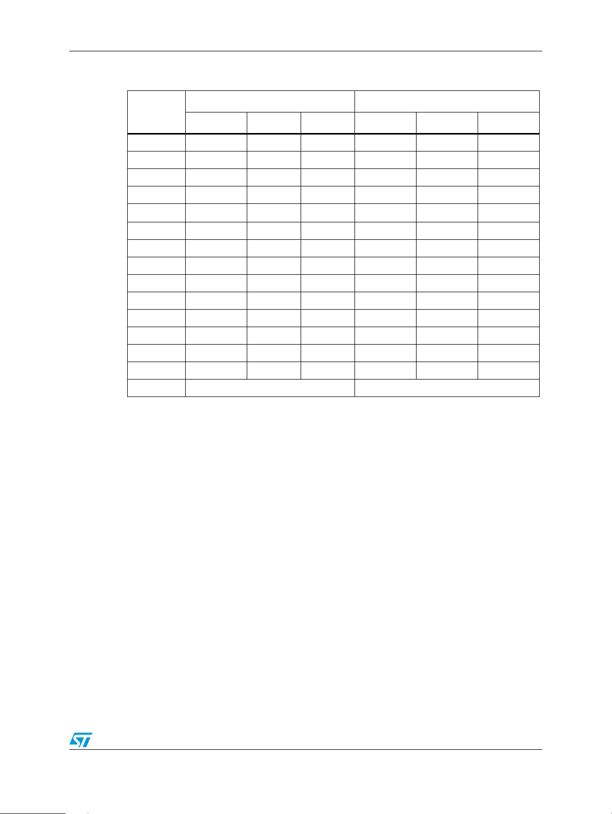
Table 1. Device summary
Order code V
(1)
(V) V
RST1
(V) t
RST2
(ms) Package
REC
STM6905TZEDS6F 3.078 2.333 210 MSOP8(TSSOP8)
STM6905TWEDS6F 3.078 1.683 210 MSOP8(TSSOP8)
STM6905TGEDS6F 3.078 1.110 210 MSOP8(TSSOP8)
STM6905SYEDS6F 2.955 2.188 210 MSOP8(TSSOP8)
STM6905SFEDS6F 2.955 1.050 210 MSOP8(TSSOP8)
STM6905PWEDS6F 2.866 1.683 210 MSOP8(TSSOP8)
1. Other reset threshold voltages and t
ST sales office for availability.
time-out periods are offered. Minimum order quantities may apply. Contact local
REC
January 2008 Rev 3 1/19
www.st.com
1

Contents STM6905
Contents
1 Description . . . . . . . . . . . . . . . . . . . . . . . . . . . . . . . . . . . . . . . . . . . . . . . . . 5
2 Pin descriptions . . . . . . . . . . . . . . . . . . . . . . . . . . . . . . . . . . . . . . . . . . . . 7
2.1 Push-button reset input (MR) . . . . . . . . . . . . . . . . . . . . . . . . . . . . . . . . . . . 7
2.2 V
2.3 V2IN second fixed voltage monitoring input . . . . . . . . . . . . . . . . . . . . . . . . 7
2.4 V
2.5 V3IN, V4IN, and V5IN . . . . . . . . . . . . . . . . . . . . . . . . . . . . . . . . . . . . . . . . 7
2.6 RST
primary supply voltage monitoring input . . . . . . . . . . . . . . . . . . . . . . . 7
CC
SS . . . . . . . . . . . . . . . . . . . . . . . . . . . . . . . . . . . . . . . . . . . . . . . . . . . . . . . . . . . . . . . . . . . . . 7
active-low, open drain reset output . . . . . . . . . . . . . . . . . . . . . . . . . . . 7
3 Operation . . . . . . . . . . . . . . . . . . . . . . . . . . . . . . . . . . . . . . . . . . . . . . . . . . 9
3.1 Setting the adjustable voltage levels for V3IN, V4IN, and V5IN inputs . . . . 9
3.2 Power on reset (t
) . . . . . . . . . . . . . . . . . . . . . . . . . . . . . . . . . . . . . . . . . 9
REC
4 Voltage monitoring . . . . . . . . . . . . . . . . . . . . . . . . . . . . . . . . . . . . . . . . . 10
5 Maximum rating . . . . . . . . . . . . . . . . . . . . . . . . . . . . . . . . . . . . . . . . . . . . 11
6 DC and AC parameters . . . . . . . . . . . . . . . . . . . . . . . . . . . . . . . . . . . . . . 12
7 Package mechanical data . . . . . . . . . . . . . . . . . . . . . . . . . . . . . . . . . . . . 14
8 Part numbering . . . . . . . . . . . . . . . . . . . . . . . . . . . . . . . . . . . . . . . . . . . . 16
9 Package marking information . . . . . . . . . . . . . . . . . . . . . . . . . . . . . . . . 17
10 Revision history . . . . . . . . . . . . . . . . . . . . . . . . . . . . . . . . . . . . . . . . . . . 18
2/19

STM6905 List of tables
List of tables
Table 1. Device summary . . . . . . . . . . . . . . . . . . . . . . . . . . . . . . . . . . . . . . . . . . . . . . . . . . . . . . . . . . 1
Table 2. Signal names and functions . . . . . . . . . . . . . . . . . . . . . . . . . . . . . . . . . . . . . . . . . . . . . . . . . 6
Table 3. Absolute maximum ratings . . . . . . . . . . . . . . . . . . . . . . . . . . . . . . . . . . . . . . . . . . . . . . . . . 11
Table 4. DC and AC characteristics . . . . . . . . . . . . . . . . . . . . . . . . . . . . . . . . . . . . . . . . . . . . . . . . . 12
Table 5. TSSOP 8-lead package mechanical data . . . . . . . . . . . . . . . . . . . . . . . . . . . . . . . . . . . . . . 15
Table 6. Ordering information scheme . . . . . . . . . . . . . . . . . . . . . . . . . . . . . . . . . . . . . . . . . . . . . . . 16
Table 7. Marking description. . . . . . . . . . . . . . . . . . . . . . . . . . . . . . . . . . . . . . . . . . . . . . . . . . . . . . . 17
Table 8. Document revision history . . . . . . . . . . . . . . . . . . . . . . . . . . . . . . . . . . . . . . . . . . . . . . . . . 18
3/19

List of figures STM6905
List of figures
Figure 1. Logic diagram . . . . . . . . . . . . . . . . . . . . . . . . . . . . . . . . . . . . . . . . . . . . . . . . . . . . . . . . . . . . 5
Figure 2. MSOP/TSSOP-8 connections. . . . . . . . . . . . . . . . . . . . . . . . . . . . . . . . . . . . . . . . . . . . . . . . 5
Figure 3. Functional block diagram . . . . . . . . . . . . . . . . . . . . . . . . . . . . . . . . . . . . . . . . . . . . . . . . . . . 8
Figure 4. Typical hardware hookup application diagram . . . . . . . . . . . . . . . . . . . . . . . . . . . . . . . . . . . 8
Figure 5. MR
Figure 6. Voltage monitoring diagram . . . . . . . . . . . . . . . . . . . . . . . . . . . . . . . . . . . . . . . . . . . . . . . . 10
Figure 7. TSSOP8, 3 x 3mm, package mechanical outline . . . . . . . . . . . . . . . . . . . . . . . . . . . . . . . . 14
timing waveforms . . . . . . . . . . . . . . . . . . . . . . . . . . . . . . . . . . . . . . . . . . . . . . . . . . . . . 10
4/19
STM6905 Description
1 Description
The STM6905 supervisor is a low voltage/low supply current processor supervisor,
designed to monitor up to five system power supply voltages. This device is targeted at
applications such as set-top boxes (STBs), portable, battery-powered systems, networking
and communication systems.
The device supports a push-button type manual reset input (MR
monitors (V
(V
RST1
and V
and V2IN) have fixed (customer-selectable, factory-trimmed) thresholds
CC
). The other three voltage monitor inputs (V3IN, V4IN and V5IN) are
RST2
). Two of the five supply
monitored using externally adjustable threshold (600 mV internal reference) to meet specific
level requirements.
If any of the five monitored voltages drops below its factory-trimmed or adjustable
thresholds, or if the MR
low). Once asserted, RST
monitored supplies rise above their respective thresholds and MR
output logic state is valid for V
is asserted to logic low, the reset output RST is asserted (driven
is maintained Low for a minimum delay period (trec) after ALL
returns to High. Reset
greater than 0.8 V.
CC
The STM6905 is available in a standard 8-lead MSOP (TSSOP) package.
Figure 1. Logic diagram
V
CC
V2IN
V3IN
V4IN
V5IN
STM6905
RST
MR
V
Figure 2. MSOP/TSSOP-8 connections
MR
V
CC
V2IN
V
SS
1
2
3
4
5/19
SS
ai13970
8
7
6
5
RST
V5IN
V4IN
V3IN
ai13971
Description STM6905
Table 2. Signal names and functions
Pin Name Type Function
1MR
2VCCSupply
3 V2IN Input Second fixed threshold input monitor
4V
5 V3IN Input Adjustable third reset comparator input
6 V4IN Input Adjustable fourth reset comparator input
7 V5IN Input Adjustable fifth reset comparator input
8RST
SS
Input Active-low manual reset input with internal pull-up resistor
Primary supply voltage input and integrated fixed threshold undervoltage monitor
Supply Ground
Output Active-low open-drain reset output (10k ohm internal pull-up)
6/19

STM6905 Pin descriptions
2 Pin descriptions
2.1 Push-button reset input (MR)
When MR goes low the RST output is driven low, RST remains low as long as MR is low and
for t
resistor to V
outputs, or connected to V
V
Connect a normally open momentary switch from MR
not required. (If MR
connecting a 0.1uF capacitor from MR
2.2 VCC primary supply voltage monitoring input
The VCC pin is also the input for the primary reset threshold monitor. Fixed (customerselectable, factory programmed) reset thresholds include 3.078 V to 2.866 V.
after MR returns to high. The active-low input has an internal 10k ohm pull-up
CC
REC
.
. It can be driven from a TTL or CMOS logic line, or with open drain/collector
CC
is driven from long cables or if the device is used in noisy environments,
through a switch. If unused, leave this pin open or connect it to
SS
to VSS; external debounce circuitry is
to VSS provides additional noise immunity).
2.3 V2IN second fixed voltage monitoring input
The V2IN input is the second fixed-voltage input for reset threshold monitoring. Available
fixed (customer-selectable, factory programmed) reset thresholds include 2.333 V to
1.050 V.
2.4 V
SS
This pin is the ground pin for the power supply.
2.5 V3IN, V4IN, and V5IN
The V3IN, V4IN and V5IN are high impedance inputs. RST is driven low when the voltage
(VTRIP) at the pin falls below 600 mV (internal reference voltage at their respective
comparators). The monitored voltage reset threshold is set with an external resistor-divider
network.
2.6 RST active-low, open drain reset output
The reset output (RST) pin is driven low and stays low whenever VCC or V2IN, or V3IN, or
V4IN, or V5IN falls below its factory-trimmed or adjustable reset threshold or when MR
goes to logic low. It remains low for trec after all supply voltages being monitored rise above
their reset thresholds and MR
V
. A 10k ohms pull-up resistor should be sufficient for most applications.
CC
goes from low to high. Connect an external pull-up resistor to
7/19
Pin descriptions STM6905
Figure 3. Functional block diagram
V
CC
V
RST1
COMPARE
V2IN
V3IN
V4IN
V5IN
MR
V
RST2
V
= 0.6V
REF
V
= 0.6V
REF
V
REF
V
CC
(1)
= 0.6V
COMPARE
COMPARE
COMPARE
COMPARE
1. Internal pull-up on MR input of 10k ohm (typ).
Figure 4. Typical hardware hookup application diagram
From DC/DC Converter
V
=
(600mV)
TRIP
V =
(600mV)
TRIP
V =
(600mV)
TRIP
R1 + R2
(
R2
R3 + R4
(
R5 + R6
(
R6
R4
R1
R2
V
CC2
)
)
)
V
CC3
0.1 F
V
CC4
R3
R4
0.1 F
R5
R6
V
V
CC1
CC5
V
CC
V
IN2
VIN3
VIN4
VIN5
STM6905
V
SS
RST
MR
t
rec
Generator
ai13970
RST (To Processor Reset)
RST
Push-button
Switch
8/19
ai13973

STM6905 Operation
3 Operation
The STM6905 provides the ability to monitor critical voltages such as power-supply and
battery voltage levels, while interfacing easily to the system controllers/microprocessors.
Figure 4 shows typical hardware hookup for monitoring five voltages; two fixed thresholds
(customer-selectable, factory-programmed ) and three adjustable monitor inputs. RST
output is open drain and requires a 10k ohms pull-up resistor tied to V
CC
.
3.1 Setting the adjustable voltage levels for V3IN, V4IN, and V5IN
inputs
The user can customize the minimum voltage levels for the three adjustable voltage inputs
by connecting an external resistor divider network to the V3IN, V4IN and V5IN pins in order
to set the trip point at some voltage above the 600 mv (V
formula.
6.0
VVTRIP
+
×=
R
) according to the following
REF
21
RR
2
During normal operation, the STM6905 monitors the voltage levels at all the five pins (Vcc,
V2IN, V3IN, V4IN and V5IN).
3.2 Power on reset (t
On power up, the STM6905 activates a power on reset circuit which asserts the reset pin
(i.e. RST
and MR
that the supply voltage has stabilized to sufficient operating levels.
goes low). The RST signal remains active until VCC (and V2IN, V3IN, V4IN, V5IN
) rises above the minimum voltage level for the time period t
REC
)
thereby ensuring
REC
9/19

Voltage monitoring STM6905
4 Voltage monitoring
Figure 5. MR timing waveforms
t
MR
RST
MLMH
t
MLMR
t
REC
ai13974
Figure 6. Voltage monitoring diagram
V
,
VXIN
CC
V
V
RST1/2
RSTIN
,
RST
t
RD
t
rec
ai13975
10/19

STM6905 Maximum rating
5 Maximum rating
Stressing the device above the rating listed in the "Absolute maximum ratings" table may
cause permanent damage to the device. These are stress ratings only and operation of the
device at these or any other conditions above those indicated in the Operating sections of
this specification is not implied. Exposure to absolute maximum rating conditions for
extended periods may affect device reliability. Refer also to the STMicroelectronics SURE
Program and other relevant quality documents.
Table 3. Absolute maximum ratings
Symbol Parameter Value Unit
T
STG
T
SLD
V
IO
V
CC
I
O
θ
JA
1. Reflow at peak temperature of 255°C to 260°C for < 30 seconds (total thermal budget not to exceed
180°C for between 90 to 150 seconds).
Storage temperature (VCC off) -55 to +150 °C
(1)
Lead solder temperature for 10 seconds 260 °C
Input or output voltage -0.3 to VCC +0.3 V
Supply voltage -0.3 to 7.0 V
Output current 20 mA
Thermal resistance (junction to ambient) 146 °C/W
11/19

DC and AC parameters STM6905
6 DC and AC parameters
This section summarizes the operating measurement conditions and the DC and AC
characteristics of the device. Designers should check that the operating conditions in their
circuit match the operating conditions when relying on the quoted parameters.
Table 4. DC and AC characteristics
Sym
V
CC
I
CC
Alter-
native
Description Test condition
Operating voltage 0.8 5.5 V
V
< 5.5 V 12 16
VCC supply current
CC
= 3.3 V 11 15
V
CC
(1)
Min Typ Max Unit
I2IN V2IN supply curent V2IN = 3.3 V 3 5 µA
I
LI
(3)
I
LO
V
OL
Input leakage current -
(2)
)
(MR
Open drain RST output
leakage current
Output low voltage
; open drain)
(RST
VIN = V
V
CC
not asserted
RST
VCC ≥ 0.8V, I
≥ 1.0V, I
V
CC
V
≥ 1.2V, I
CC
≥ 2.7V, I
V
CC
≥ 4.5V, I
V
CC
or VSS -0.5 +0.5 µA
CC
> VRST;
= 1 µA 0.3 V
SINK
= 50 µA 0.3 V
SINK
= 100 µA 0.3 V
SINK
= 1.2 mA 0.3 V
SINK
= 3.2 mA 0.4 V
SINK
-0.5 +0.5 µA
25°C 3.047 3.078 3.109 V
T (falling)
-40°C to 85°C 3.023 3.133
V
RST1
(4)
V
TH1VCC
reset threshold
S (falling)
25°C 2.925 2.955 2.985 V
-40°C to 85°C 2.902 3.008
25°C 2.837 2.866 2.895 V
P (falling)
-40°C to 85°C 2.814 2.918
µA
Z (falling)
Y (falling)
(4)
V
RST2
V
V2IN reset threshold
TH2
W (falling)
G (falling)
F (falling)
12/19
25°C 2.310 2.333 2.356 V
-40°C to 85°C 2.291 2.375
25°C 2.166 2.188 2.210 V
-40°C to 85°C 2.149 2.227
25°C 1.666 1.683 1.700 V
-40°C to 85°C 1.653 1.713
25°C 1.099 1.110 1.121 V
-40°C to 85°C 1.090 1.130
25°C 1.040 1.050 1.061 V
-40°C to 85°C 1.031 1.069

STM6905 DC and AC parameters
Table 4. DC and AC characteristics (continued)
Sym
V
HYST
t
RD
Alter-
native
Description Test condition
Reset threshold
Referenced to V
hysteresis
V
= (V
CC
(V
VCC to RST delay
V2IN = (V
RST1
(V
t
REC
t
RST time-out period
RP
Adjustable reset comparator input (V3IN, V4IN, V5IN)
V
RSTIN
I
RSTIN
V3IN, V4IN, V5IN input
threshold
V3IN, V4IN, V5IN input
current
V3IN, V4IN, V5IN > 0.8 V –25 +25 nA
V3IN, V4IN, V5IN
hysteresis
t
RSTIND
V3IN, V4IN, V5IN to
output delay
RST
VRSTIN to (VRSTIN – 30 mV) 22 µs
typical
+ 100 mV) to
RST1
– 100 mV)
RST2
– 75 mV)
RST2
Option B
Option C
(1)
RST1/VRST2
+ 75 mV) to
(5)
(5)
Min Typ Max Unit
0.5 %
20 µs
20 µs
20 30 40 ms
80 120 180 ms
Option E 140 210 280 ms
Option F
(5)
280 420 560 ms
589 600 611 mV
3mV
Manual (push-button) reset input
V
IL
V
IH
t
MLMH
t
MLRL
1. Valid for ambient operating temperature: TA = –40°C to +85°C; VCC = 0.8 V to 5.5 V (except where noted).
2. 10k ohm (typ) internal pull-up resistor.
3. The leakage current measured on the RST
4. Other reset threshold voltages are offered. Minimum order quantities may apply. Contact local sales office for availability.
5. Other t
t
REC
MR input voltage
0.7 x V
CC
MR minimum pulse
t
MR
width
MR to RST output delay 200 ns
MRD
MR
glitch immunity 100 ns
pull-up resistance 10 kΩ
MR
pin is tested with the reset de-asserted (output high impedance).
time-out periods are offered. Minimum order quantities may apply. Contact local sales office for availability.
1µs
0.3 x V
CC
V
V
13/19

Package mechanical data STM6905
7 Package mechanical data
In order to meet environmental requirements, ST offers these devices in ECOPACK
®
packages. These packages have a lead-free second level interconnect. The category of
second level interconnect is marked on the package and on the inner box label, in
compliance with JEDEC Standard JESD97. The maximum ratings related to soldering
conditions are also marked on the inner box label. ECOPACK is an ST trademark.
ECOPACK specifications are available at: www.st.com.
Figure 7. TSSOP8, 3 x 3mm, package mechanical outline
D
8
1
ccc
5
EE1
4
A2A
A1
L
L1
c
k
L2
eb
E3_ME
14/19
STM6905 Package mechanical data
Table 5. TSSOP 8-lead package mechanical data
mm inches
Symbol
Min Typ Max Min Typ Max
A 1.100 0.043
A1 0.00 0.15 0.000 0.006
A2 0.75 0.85 0.95 0.030 0.034 0.037
b 0.22 0.40 0.009 0.016
c 0.08 0.23 0.003 0.009
ccc 0.10 0.004
D 2.80 3.00 3.20 0.110 0.118 0.126
e 0.65 0.026
E 4.65 4.90 5.15 0.183 0.193 0.203
E1 2.80 3.00 3.10 0.110 0.118 0.122
L 0.40 0.60 0.80 0.016 0.024 0.032
L1 0.95 0.037
L2 0.25 0.010
k0
N8 8
° 46° 0° 46°
15/19
Part numbering STM6905
8 Part numbering
Table 6. Ordering information scheme
Example: STM6905 TZ E DS 6 F
Device type
STM6905
Reset threshold voltages
Suffix V
RST1
V
RST2
TZ 3.078 2.333
TW 3.078 1.683
TG 3.078 1.110
SY 2.955 1.050
SF 2.955 1.050
PW 2.866 1.683
t
REC
B = 30 ms
C = 120 ms
(1)
(1)
E = 210 ms
F = 420 ms
(1)
Package
DS = MSOP8 (TSSOP8)
(1)
Temperature range
6: -40°C to 85°C
Shipping method
E = ECOPACK
F = ECOPACK
1. Other reset threshold voltages and t
apply. Contact local sales office for availability.
®
package, tubes
®
package, tape & reel
time-out periods are offered. Minimum order quantities may
REC
16/19
STM6905 Package marking information
9 Package marking information
Table 7. Marking description
Part marking V
STM6905TZEDS6F 3.078 2.333 MSOP (TSSOP8) STZE
STM6905TWEDS6F 3.078 1.683 MSOP (TSSOP8) STWE
STM6905TGEDS6F 3.078 1.110 MSOP (TSSOP8) STGE
STM6905SYEDS6F 2.955 2.188 MSOP (TSSOP8) SSYE
STM6905SFEDS6F 2.955 1.050 MSOP (TSSOP8) SSFE
STM6905PWEDS6F 2.866 1.683 MSOP (TSSOP8) SPWE
(V) V
RST1
(V) Package Topside marking
RST2
17/19
Revision history STM6905
10 Revision history
Table 8. Document revision history
Date Revision Changes
19-Dec-2007 1 Initial release.
23-Jan-2008 2 Document status upgraded to full datasheet.
28-Jan-2008 3 Updated cover page, Figure 6, and Ta b l e 4.
18/19

STM6905
Please Read Carefully:
Information in this document is provided solely in connection with ST products. STMicroelectronics NV and its subsidiaries (“ST”) reserve the
right to make changes, corrections, modifications or improvements, to this document, and the products and services described herein at any
time, without notice.
All ST products are sold pursuant to ST’s terms and conditions of sale.
Purchasers are solely responsible for the choice, selection and use of the ST products and services described herein, and ST assumes no
liability whatsoever relating to the choice, selection or use of the ST products and services described herein.
No license, express or implied, by estoppel or otherwise, to any intellectual property rights is granted under this document. If any part of this
document refers to any third party products or services it shall not be deemed a license grant by ST for the use of such third party products
or services, or any intellectual property contained therein or considered as a warranty covering the use in any manner whatsoever of such
third party products or services or any intellectual property contained therein.
UNLESS OTHERWISE SET FORTH IN ST’S TERMS AND CONDITIONS OF SALE ST DISCLAIMS ANY EXPRESS OR IMPLIED
WARRANTY WITH RESPECT TO THE USE AND/OR SALE OF ST PRODUCTS INCLUDING WITHOUT LIMITATION IMPLIED
WARRANTIES OF MERCHANTABILITY, FITNESS FOR A PARTICULAR PURPOSE (AND THEIR EQUIVALENTS UNDER THE LAWS
OF ANY JURISDICTION), OR INFRINGEMENT OF ANY PATENT, COPYRIGHT OR OTHER INTELLECTUAL PROPERTY RIGHT.
UNLESS EXPRESSLY APPROVED IN WRITING BY AN AUTHORIZED ST REPRESENTATIVE, ST PRODUCTS ARE NOT
RECOMMENDED, AUTHORIZED OR WARRANTED FOR USE IN MILITARY, AIR CRAFT, SPACE, LIFE SAVING, OR LIFE SUSTAINING
APPLICATIONS, NOR IN PRODUCTS OR SYSTEMS WHERE FAILURE OR MALFUNCTION MAY RESULT IN PERSONAL INJURY,
DEATH, OR SEVERE PROPERTY OR ENVIRONMENTAL DAMAGE. ST PRODUCTS WHICH ARE NOT SPECIFIED AS "AUTOMOTIVE
GRADE" MAY ONLY BE USED IN AUTOMOTIVE APPLICATIONS AT USER’S OWN RISK.
Resale of ST products with provisions different from the statements and/or technical features set forth in this document shall immediately void
any warranty granted by ST for the ST product or service described herein and shall not create or extend in any manner whatsoever, any
liability of ST.
ST and the ST logo are trademarks or registered trademarks of ST in various countries.
Information in this document supersedes and replaces all information previously supplied.
The ST logo is a registered trademark of STMicroelectronics. All other names are the property of their respective owners.
© 2008 STMicroelectronics - All rights reserved
STMicroelectronics group of companies
Australia - Belgium - Brazil - Canada - China - Czech Republic - Finland - France - Germany - Hong Kong - India - Israel - Italy - Japan -
Malaysia - Malta - Morocco - Singapore - Spain - Sweden - Switzerland - United Kingdom - United States of America
www.st.com
19/19
 Loading...