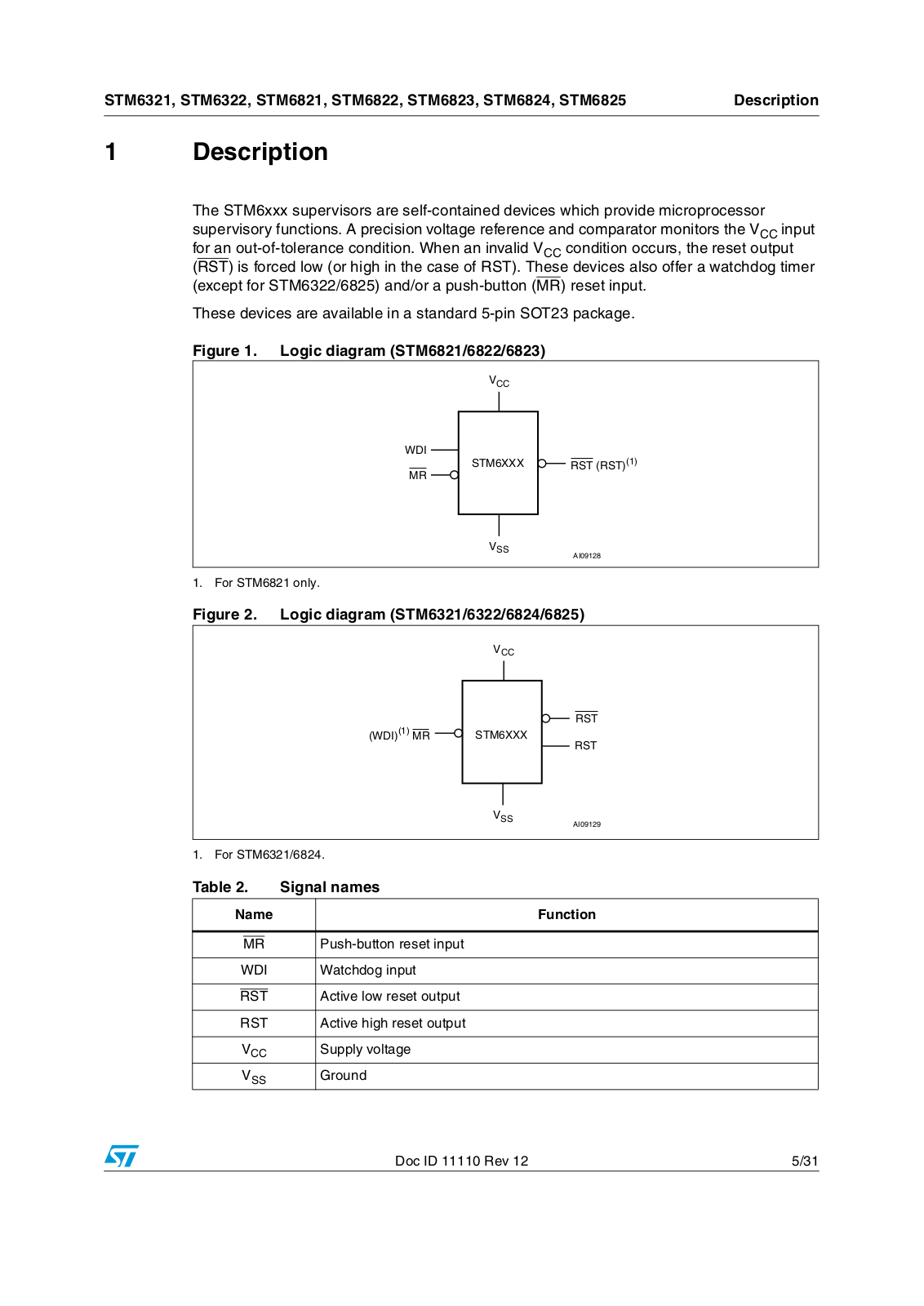
How it Works
Log In / Sign Up
Buy Points
How it Works
FAQ
Contact Us
Questions and Suggestions
Users
ST
Loading...
S
STM32L162ZD
STM32L4
STM32L4R9I-EVAL
STM32L4 Series
3
STM32L4x6
STM32MP157A-DK1
STM32MP157A-EV1
STM32MP157C-DK2
STM32MP157C-EV1
STM32MP157 Series
STM32TS60
STM32VL
STM32W108C8
2
STM32W108CB
2
STM32W108CC
STM32W108CZ
STM32W108HB
2
STM32W-EXT
STM32W-SK
STM351-2
STM6315
STm6316
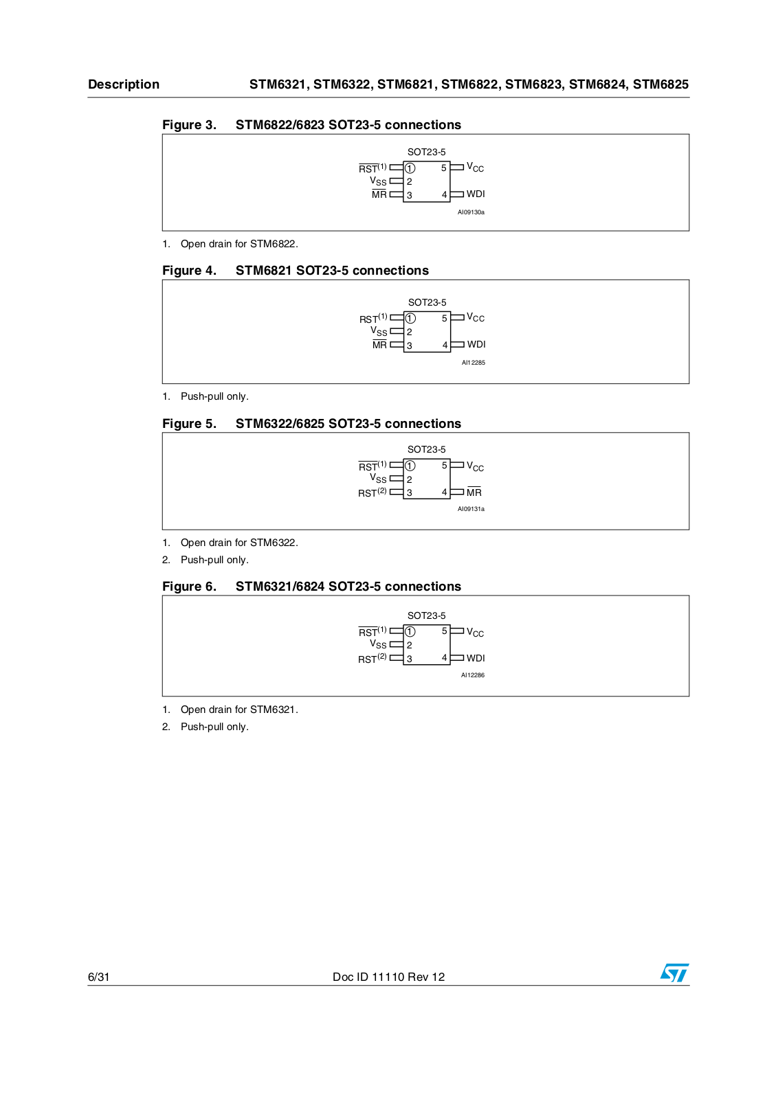
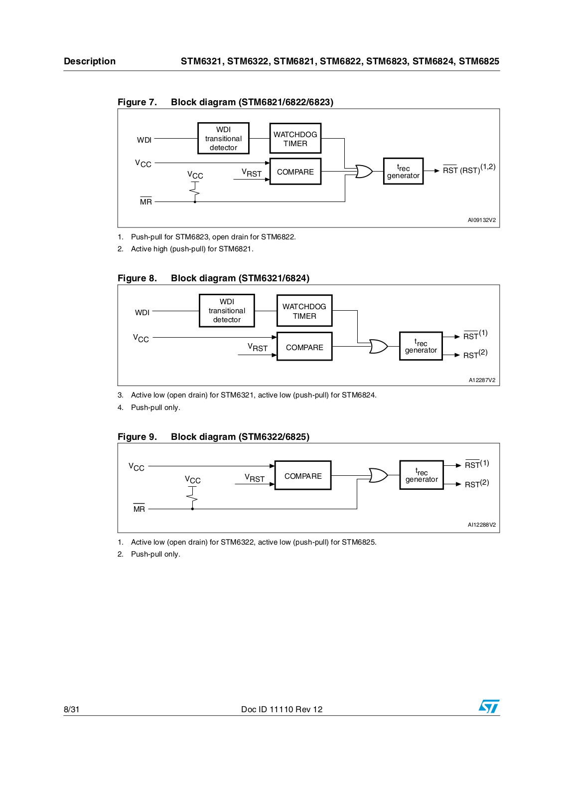
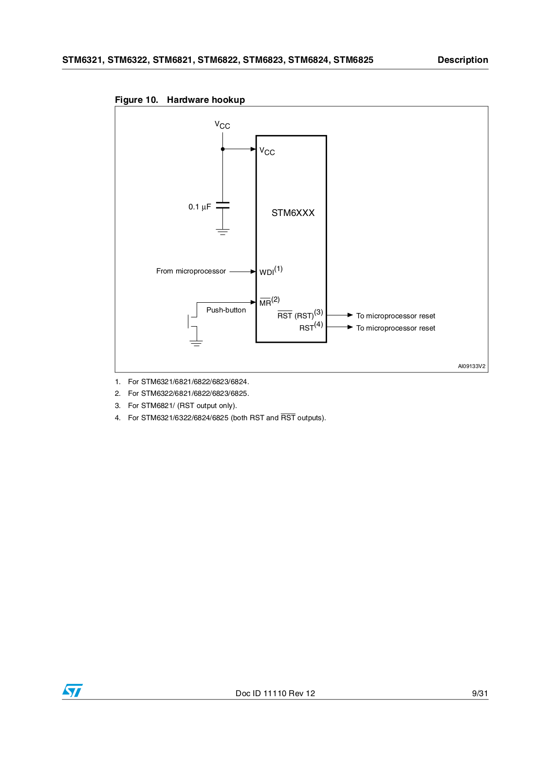
STM6321
STM6322
STM6502
STM6503
STM6504
STM6505
STM6510
STM6513
STM6519
STM6520
STM6522
STM6524
STM6600
STM6601
STM6700
STM6710
STM6717
STM6718
STM6719
STM6720
STM6777
STM6778
STM6779
STM6780
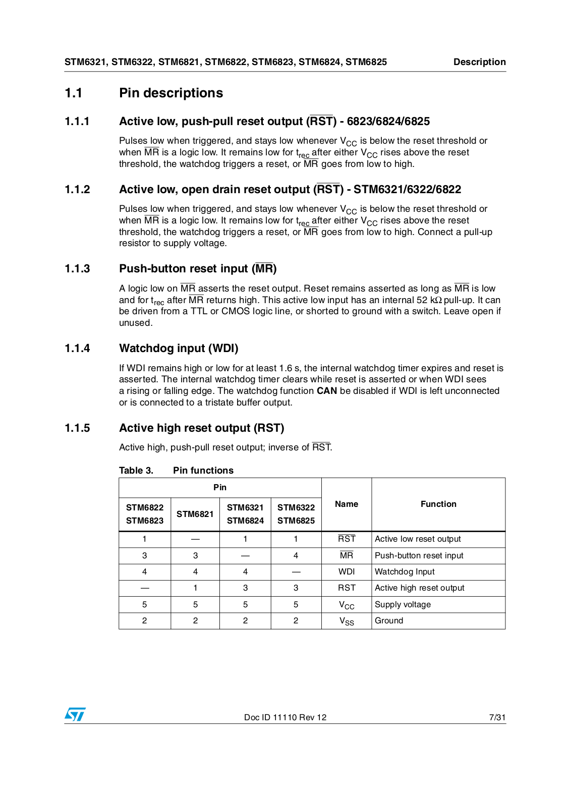
STM6821
STM6822
STM6823
STM6824
STM6825
STM690
STM6904
STM6905
STM690A
STM692A
STM7007
STM703
STM704
2
STM705
STM706
STM706P
2
STM706R
2
STM706S
2
STM706T
2
STM707
STM708
STM708R
2
STM708S
2
STM708T
2
STM795
STM8
2
STM802
2
STM804
STM805
2
STM806
STM809
STM810
STM811
STM812
STM8-128
STM8-128-EVAL
STM8-128-MCKIT
STM813L
STM817
STM818
STM819
STM86312
STM8A
STM8A-128
STM8A-DISCOVERY
STM8AF5168
STM8AF5169
STM8AF5178
STM8AF5179
STM8AF5188
STM8AF5189
STM8AF518A
STM8AF5198
STM8-TOUCH-LIB
Loading...
Loading...
Nothing found
STM6825
User Manual
31 pgs
382.04 Kb
0
Table of contents
Loading...
ST STM6321, STM6322, STM6821, STM6822, STM6823 User Manual
...
ST STM6321, STM6322, STM6821, STM6822, STM6823, STM6824, STM6825 User Manual
Download
Specifications and Main Features
Frequently Asked Questions
User Manual
Download
Loading...
+
21
hidden pages
Unhide
You need points to download manuals.
1 point = 1 manual.
You can buy points or you can get point for every manual you upload.
Buy points
Upload your manuals