

Features
STM6717/6718/6719/6720
STM6777/6778/6779/6780
Dual/triple ultra-low voltage supervisors
with push-button reset (with delay option)
■ Primary supply (V
) monitor.
CC1
Fixed (factory-programmed) reset thresholds:
4.63 V to 1.58 V
■ Secondary supply (V
) monitor
CC2
(STM6717/18/19/20/77/78)
■ Fixed (factory-programmed) reset thresholds:
3.08 V to 0.79 V
■ Tertiary supply monitor (using externally
adjustable RSTIN): 0.626 V internal reference
■ RST outputs (push-pull or open drain); state
guaranteed if V
■ Reset delay time (t
CC1
or V
rec
≥ 0.8 V
CC2
) on power-up: 13.2 ms,
210 ms, 900 ms (typ)
■ Manual reset input (MR)
■ Optional delayed manual reset input (MRC)
with external capacitor (STM6777/78/79/80)
■ Low supply current - 11 µA (typ),
V
= V
CC1
■ Operating temperature: –40 °C to 85 °C
CC2
= 3.6 V
(industrial grade)
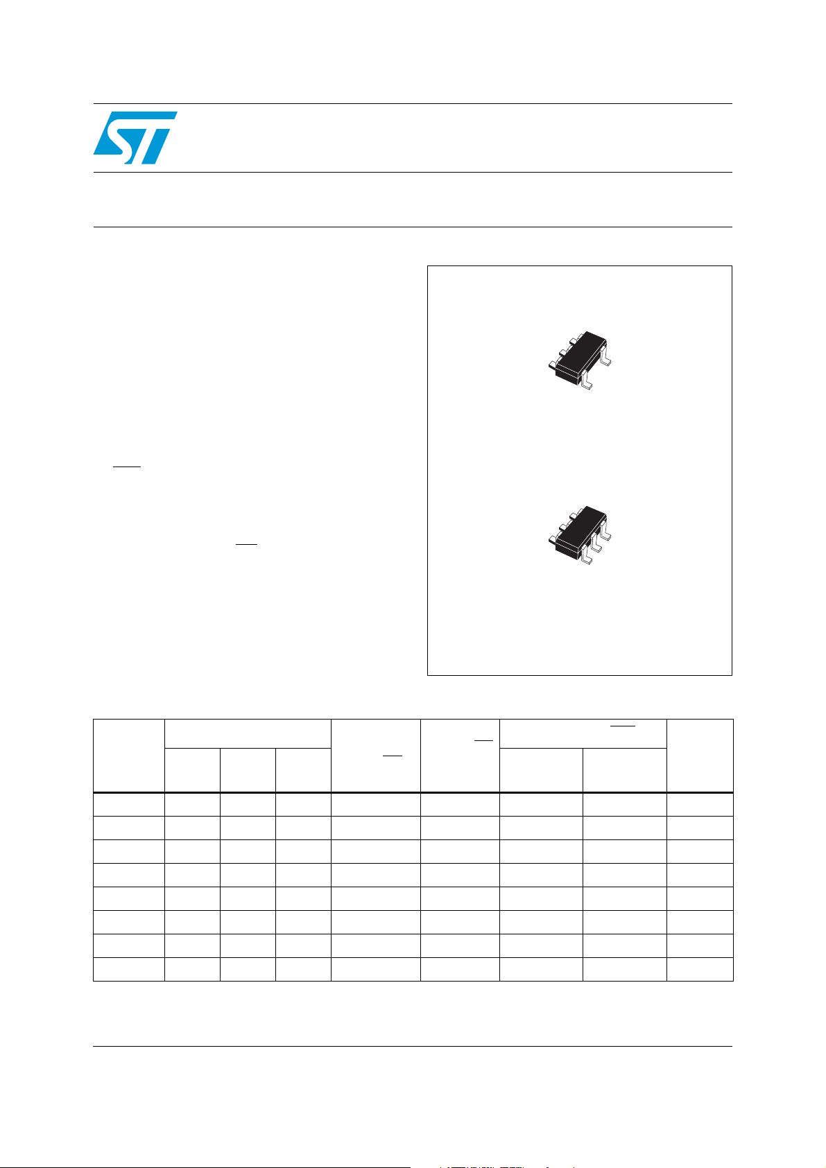
Table 1. Device summary
SOT23-5 (WY)
SOT23-6 (WB)
Monitored voltages
Part
number
STM6717 ✔✔ ✔ ✔ WY
STM6718 ✔✔ ✔ ✔ WY
STM6719 ✔✔✔ ✔ ✔ WB
STM6720 ✔✔✔ ✔ ✔ WB
STM6777 ✔✔ ✔ ✔ ✔ WB
STM6778 ✔✔ ✔ ✔ ✔ WB
STM6779 ✔✔✔✔ ✔WB
STM6780 ✔✔✔✔✔ WB
August 2011 Doc ID 11469 Rev 8 1/30
V
CC1
V
CC2
RSTIN
Manual reset
input (MR)
Delayed MR
pin (MRC)
Reset output (RST
Active-low
(push-pull)
(open drain)
)
Active-low
Package
www.st.com
1

Contents STM6717/6718/6719/6720/STM6777/6778/6779/6780
Contents
1 Description . . . . . . . . . . . . . . . . . . . . . . . . . . . . . . . . . . . . . . . . . . . . . . . . . 5
1.1 Pin descriptions . . . . . . . . . . . . . . . . . . . . . . . . . . . . . . . . . . . . . . . . . . . . . 7
1.1.1 Active-low, push-pull reset output (RST) - STM6718/20/78/80 . . . . . . . . 7
1.1.2 Active-low, open drain reset output (RST
1.1.3 Push-button reset input (MR
1.1.4 Manual reset delay input (MRC) - STM6777/78/79/80) . . . . . . . . . . . . . . 8
1.1.5 Primary supply voltage monitoring input (V
1.1.6 Secondary supply voltage monitoring input (V
1.1.7 Adjustable reset comparator input (RSTIN; STM6719/20/79/80) . . . . . . 8
) . . . . . . . . . . . . . . . . . . . . . . . . . . . . . . . . . . 7
) - STM6717/19/77/79 . . . . . . . 7
) . . . . . . . . . . . . . . . . . . . 8
CC1
) . . . . . . . . . . . . . . . . . 8
CC2
2 Operation . . . . . . . . . . . . . . . . . . . . . . . . . . . . . . . . . . . . . . . . . . . . . . . . . 10
2.1 Applications information . . . . . . . . . . . . . . . . . . . . . . . . . . . . . . . . . . . . . . 10
3 Typical operating characteristics . . . . . . . . . . . . . . . . . . . . . . . . . . . . . 11
4 Maximum rating . . . . . . . . . . . . . . . . . . . . . . . . . . . . . . . . . . . . . . . . . . . . 17
5 DC and AC parameters . . . . . . . . . . . . . . . . . . . . . . . . . . . . . . . . . . . . . . 18
6 Package mechanical data . . . . . . . . . . . . . . . . . . . . . . . . . . . . . . . . . . . . 22
7 Part numbering . . . . . . . . . . . . . . . . . . . . . . . . . . . . . . . . . . . . . . . . . . . . 26
8 Revision history . . . . . . . . . . . . . . . . . . . . . . . . . . . . . . . . . . . . . . . . . . . 29
2/30 Doc ID 11469 Rev 8

STM6717/6718/6719/6720/STM6777/6778/6779/6780 List of tables
List of tables
Table 1. Device summary . . . . . . . . . . . . . . . . . . . . . . . . . . . . . . . . . . . . . . . . . . . . . . . . . . . . . . . . . . 1
Table 2. Signal names . . . . . . . . . . . . . . . . . . . . . . . . . . . . . . . . . . . . . . . . . . . . . . . . . . . . . . . . . . . . 6
Table 3. Pin functions . . . . . . . . . . . . . . . . . . . . . . . . . . . . . . . . . . . . . . . . . . . . . . . . . . . . . . . . . . . . . 8
Table 4. Absolute maximum ratings . . . . . . . . . . . . . . . . . . . . . . . . . . . . . . . . . . . . . . . . . . . . . . . . . 17
Table 5. Operating and AC measurement conditions . . . . . . . . . . . . . . . . . . . . . . . . . . . . . . . . . . . . 18
Table 6. DC and AC characteristics . . . . . . . . . . . . . . . . . . . . . . . . . . . . . . . . . . . . . . . . . . . . . . . . . 19
Table 7. t
Table 8. SOT23-5 – 5-lead small outline transistor package mechanical data. . . . . . . . . . . . . . . . . 23
Table 9. SOT23-6 – 6-lead small outline transistor package mechanical data. . . . . . . . . . . . . . . . . 24
Table 10. Carrier tape dimensions for SOT23-5L and SOT23-6L . . . . . . . . . . . . . . . . . . . . . . . . . . . 25
Table 11. Ordering information scheme . . . . . . . . . . . . . . . . . . . . . . . . . . . . . . . . . . . . . . . . . . . . . . . 26
Table 12. Marking description. . . . . . . . . . . . . . . . . . . . . . . . . . . . . . . . . . . . . . . . . . . . . . . . . . . . . . . 27
Table 13. Document revision history . . . . . . . . . . . . . . . . . . . . . . . . . . . . . . . . . . . . . . . . . . . . . . . . . 29
minimum pulse width . . . . . . . . . . . . . . . . . . . . . . . . . . . . . . . . . . . . . . . . . . . . . . . . 21
MLMH
Doc ID 11469 Rev 8 3/30

List of figures STM6717/6718/6719/6720/STM6777/6778/6779/6780
List of figures
Figure 1. Logic diagram (STM6717/18) . . . . . . . . . . . . . . . . . . . . . . . . . . . . . . . . . . . . . . . . . . . . . . . . 6
Figure 2. Logic diagram (STM6777/78) . . . . . . . . . . . . . . . . . . . . . . . . . . . . . . . . . . . . . . . . . . . . . . . . 6
Figure 3. Logic diagram (STM6719/20) . . . . . . . . . . . . . . . . . . . . . . . . . . . . . . . . . . . . . . . . . . . . . . . . 6
Figure 4. Logic diagram (STM6779/80) . . . . . . . . . . . . . . . . . . . . . . . . . . . . . . . . . . . . . . . . . . . . . . . . 6
Figure 5. STM6717/18 SOT23-5 connections . . . . . . . . . . . . . . . . . . . . . . . . . . . . . . . . . . . . . . . . . . . 7
Figure 6. STM6777/78 SOT23-6 connections . . . . . . . . . . . . . . . . . . . . . . . . . . . . . . . . . . . . . . . . . . . 7
Figure 7. STM6719/20 SOT23-6 connections . . . . . . . . . . . . . . . . . . . . . . . . . . . . . . . . . . . . . . . . . . . 7
Figure 8. STM6779/80 SOT23-6 connections . . . . . . . . . . . . . . . . . . . . . . . . . . . . . . . . . . . . . . . . . . . 7
Figure 9. Block diagram . . . . . . . . . . . . . . . . . . . . . . . . . . . . . . . . . . . . . . . . . . . . . . . . . . . . . . . . . . . . 9
Figure 10. Hardware hookup . . . . . . . . . . . . . . . . . . . . . . . . . . . . . . . . . . . . . . . . . . . . . . . . . . . . . . . . . 9
Figure 11. STM67xx interface to processor with bi-directional reset pins . . . . . . . . . . . . . . . . . . . . . . 10
Figure 12. Ensuring RST
Figure 13. Supply current vs. temperature (V
Figure 14. Supply current vs. temperature (V
Figure 15. Supply current vs. temperature (V
Figure 16. Supply current vs. temperature (V
Figure 17. Normalized V
Figure 18. Maximum V
Figure 19. Normalized V
Figure 20. Normalized V
Figure 21. Reset input threshold vs. temperature . . . . . . . . . . . . . . . . . . . . . . . . . . . . . . . . . . . . . . . . 15
Figure 22. V
-to-reset delay vs. temperature. . . . . . . . . . . . . . . . . . . . . . . . . . . . . . . . . . . . . . . . . . 15
CC1
Figure 23. Reset input-to-reset output delay vs. temperature . . . . . . . . . . . . . . . . . . . . . . . . . . . . . . . 16
Figure 24. MR
-to-reset output delay vs. temperature (V
Figure 25. AC testing input/output waveforms . . . . . . . . . . . . . . . . . . . . . . . . . . . . . . . . . . . . . . . . . . . 18
Figure 26. MR
Figure 27. MR
timing waveform (STM6717/18/19/20) . . . . . . . . . . . . . . . . . . . . . . . . . . . . . . . . . . . . . 18
timing waveform (STM6777/78/79/80) . . . . . . . . . . . . . . . . . . . . . . . . . . . . . . . . . . . . . 18
Figure 28. SOT23-5 – 5-lead small outline transistor package mechanical drawing . . . . . . . . . . . . . . 23
Figure 29. SOT23-6 – 6-lead small outline transistor package mechanical drawing . . . . . . . . . . . . . . 24
Figure 30. Carrier tape for SOT23-5L and SOT23-6L . . . . . . . . . . . . . . . . . . . . . . . . . . . . . . . . . . . . . 25
valid to VCC = 0 (active-low, push-pull outputs). . . . . . . . . . . . . . . . . . . . . . 10
= 5.5 V; V
CC1
= 3.6 V; V
CC1
= 3.0 V; V
CC1
= 2.0 V; V
reset time-out period vs. temperature . . . . . . . . . . . . . . . . . . . . . . . . . . . 13
CC
transient duration vs. reset threshold overdrive . . . . . . . . . . . . . . . . . . . . . 13
CC
threshold vs. temperature . . . . . . . . . . . . . . . . . . . . . . . . . . . . . . . . . . . 14
RST1
threshold vs. temperature . . . . . . . . . . . . . . . . . . . . . . . . . . . . . . . . . . . 14
RST2
CC1
CC1
= 3.6 V) . . . . . . . . . . . . . . . . . . . . . . 11
CC2
= 2.75 V) . . . . . . . . . . . . . . . . . . . . . 11
CC2
= 2.0 V) . . . . . . . . . . . . . . . . . . . . . . 12
CC2
= 1.0 V) . . . . . . . . . . . . . . . . . . . . . . 12
CC2
= 3.6V) . . . . . . . . . . . . . . . . . . . . . . . . . . 16
4/30 Doc ID 11469 Rev 8

STM6717/6718/6719/6720/STM6777/6778/6779/6780 Description
1 Description
The STM6717/18/19/20 and STM6777/78/79/80 supervisors are a family of low-voltage/lowsupply current processor (micro or DSP) supervisors, designed to monitor two (or three)
system power supply voltages. They are targeted at applications such as set-top boxes
(STBs), portable, battery-powered systems, networking, and communication systems.
All device options have a push-button-type manual reset input (MR
). The
STM6777/78/79/80 also includes an option which enables the user to delay the start of the
manual reset process from 6 µs (MRC pin left open) or more with external capacitor. The
delay is implemented by connecting the appropriately sized capacitor between the MRC pin
and V
Two of the three supplies monitored (V
factory-trimmed) thresholds (V
(typical 4 s delay with a 3.3 µF capacitor, see Table 7 on page 21).
SS
RST1
CC1
and V
and V
RST2
) have fixed (customer-selectable,
CC2
). The third voltage is monitored using an
externally adjustable RSTIN threshold (0.626 V internal reference).
If any of the three monitored voltages drop below its factory-trimmed or adjustable
thresholds, or if MR
RST
is maintained at low for a minimum delay period (t
their respective thresholds and MR
the correct reset output logic state when V
is asserted to logic low, a RST is asserted (driven low). Once asserted,
) after ALL supplies rise above
rec
returns to high. These devices are guaranteed to be in
CC1
and/or V
is greater than 0.8 V.
CC2
These devices are available in standard 5-pin or 6-pin SOT23 packages (see Tab le 1 o n
page 1).
Doc ID 11469 Rev 8 5/30
Description STM6717/6718/6719/6720/STM6777/6778/6779/6780
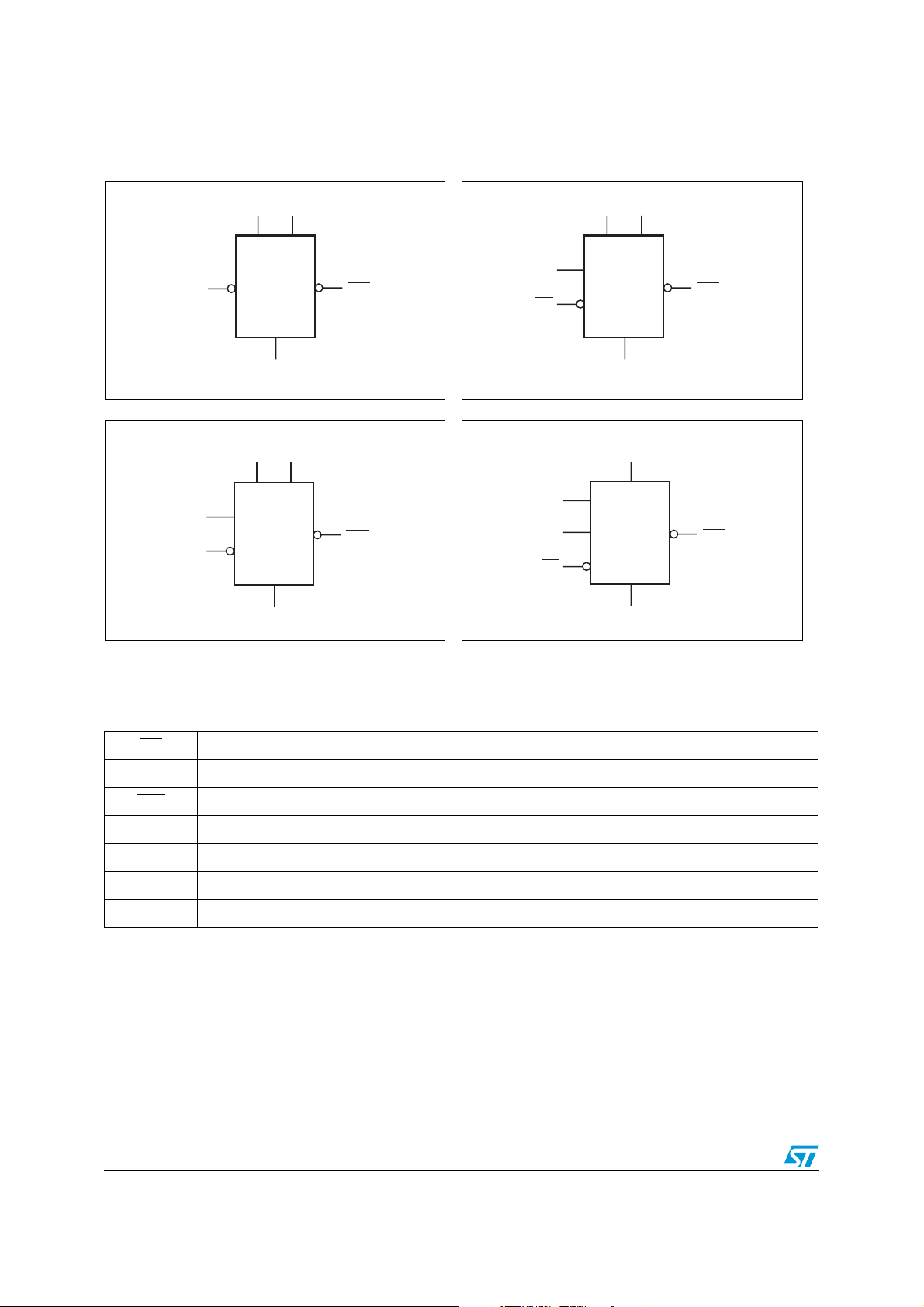
Figure 1. Logic diagram (STM6717/18) Figure 2. Logic diagram (STM6777/78)
V
V
CC1
CC2
V
V
CC1
CC2
MRC
MR
STM6777
STM6778
V
SS
RST
MR
STM6717
STM6718
V
SS
RST
AI10413
Figure 3. Logic diagram (STM6719/20) Figure 4. Logic diagram (STM6779/80)
V
CC
STM6779
STM6780
V
SS
RST
RSTIN
MR
V
CC2
STM6719
STM6720
V
SS
V
CC1
RSTIN
RST
AI10414
MRC
MR
AI10415
AI10416
Table 2. Signal names
MR Push-button reset input
MRC Manual reset delay input
RST Active-low reset output
V
CC1
V
CC2
RSTIN Adjustable reset comparator input
V
SS
6/30 Doc ID 11469 Rev 8
Primary supply voltage input
Secondary supply voltage input
Ground
STM6717/6718/6719/6720/STM6777/6778/6779/6780 Description
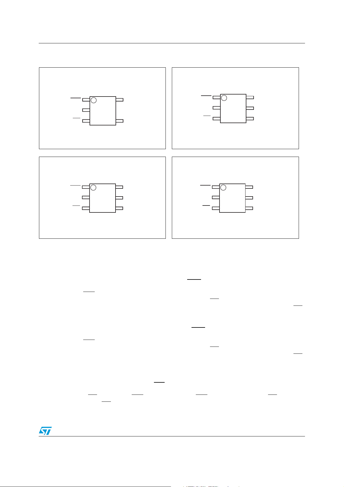
Figure 5. STM6717/18 SOT23-5 connections Figure 6. STM6777/78 SOT23-6 connections
V
RST
V
SS
MR
SS
1
2
3
V
1
2
3
5
CC1
V
4
CC2
RST
V
MR
6
CC1
5
MRC
V
4
CC2
AI10417
AI10418
Figure 7. STM6719/20 SOT23-6 connections Figure 8. STM6779/80 SOT23-6 connections
RST
V
SS
MR
V
1
2
3
6
5
CC1
RSTIN
V
4
CC2
AI10419
RST
V
MR
SS
1
2
3
V
6
CC1
RSTIN
5
MRC
4
AI10420
1.1 Pin descriptions
1.1.1 Active-low, push-pull reset output (RST) - STM6718/20/78/80
The RST pin is driven low and stays low whenever V
factory-trimmed or adjustable reset threshold or when MR
for t
after ALL supply voltages being monitored rise above their reset thresholds and MR
rec
goes from low to high. (Push-pull outputs are referenced to V
CC1
or V
or RSTIN falls below its
CC2
goes to logic low. It remains low
.)
CC1
1.1.2 Active-low, open drain reset output (RST) - STM6717/19/77/79
The RST pin is driven low and stays low whenever V
factory-trimmed or adjustable reset threshold or when MR
for t
after ALL supply voltages being monitored rise above their reset thresholds and MR
rec
goes from low to high. Connect an external pull-up resistor to V
should be sufficient for most applications.
CC1
or V
or RSTIN falls below its
CC2
goes to logic low. It remains low
. A 10 kΩ pull-up resistor
CC1
1.1.3 Push-button reset input (MR)
When MR goes low the RST output is driven low. RST remains low as long as MR is low and
for t
after MR returns to high. This active-low input has an internal 50 kΩ pull-up resistor to
rec
Doc ID 11469 Rev 8 7/30
Description STM6717/6718/6719/6720/STM6777/6778/6779/6780
V
. It can be driven from a TTL or CMOS logic line, or with open drain/collector outputs,
CC1
or connected to V
Connect a normally open momentary switch from MR
not required. (If MR
connecting a 0.1µF capacitor from MR
through a switch. If unused, leave this pin open or connect it to V
SS
CC1
to VSS; external debounce circuitry is
is driven from long cables or if the device is used in noisy environments,
to VSS provides additional noise immunity.
.
1.1.4 Manual reset delay input (MRC) - STM6777/78/79/80)
This pin is either left open or connected to VSS via a capacitor. By selecting the appropriate
capacitor, the manual reset process, initiated by pressing the push-button manual reset
input, can be delayed by any value from 6 µs or more (see Table 7 on page 21).
1.1.5 Primary supply voltage monitoring input (V
CC1
)
It also is the input for the primary reset threshold monitor. Available fixed (customerselectable, factory-programmed) reset thresholds include 4.63 V to 1.58 V.
1.1.6 Secondary supply voltage monitoring input (V
CC2
)
This function is available on the STM6717/18/19/20/77/78. Fixed (customer-selectable,
factory-programmed) reset thresholds include 3.08 V to 0.79 V.
1.1.7 Adjustable reset comparator input (RSTIN; STM6719/20/79/80)
This is a high impedance input. RST is driven low when the voltage at the RSTIN pin falls
below 0.626 V (internal reference voltage at this comparator). The monitored voltage reset
threshold is set with an external resistor-divider network.
Table 3. Pin functions
Pin
STM6717
STM6718
1111RST
3333MR
— — 5 4 MRC Manual reset delay input
STM6719
STM6720
STM6777
STM6778
STM6779
STM6780
Name Function
Active-low reset output
Push-button reset input
5666V
444—V
— 5 — 5 RSTIN Adjustable reset comparator input
2222V
8/30 Doc ID 11469 Rev 8
Primary supply voltage input
CC1
Secondary supply voltage input
CC2
Ground
SS
STM6717/6718/6719/6720/STM6777/6778/6779/6780 Description
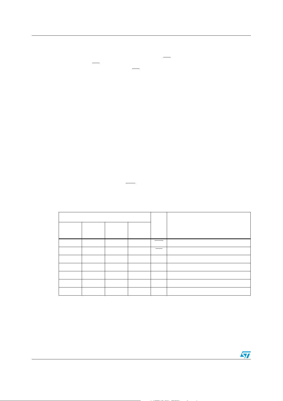
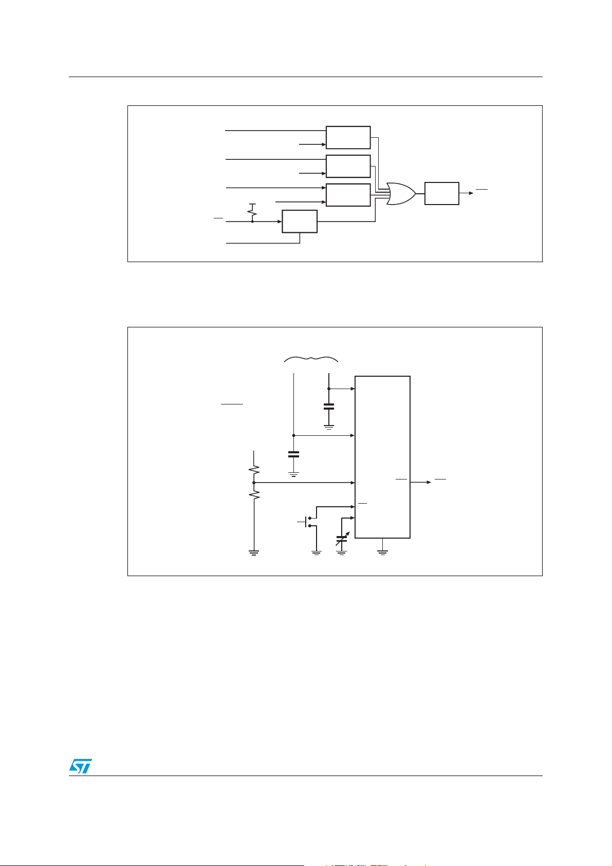
Figure 9. Block diagram
V
V
CC2
RSTIN
CC1
V
(1)
V
(2)
V
= 0.626
V
CC1
REF/2
RST1
RST2
COMPARE
COMPARE
COMPARE
t
rec
Generator
RST
Logic
1. V
MR
(3)
MRC
input is available on STM6717/18/19/20/77/78.
CC2
2. RSTIN available only on STM6719/20/79/80.
3. MRC available only on STM6777/78/79/80.
Figure 10. Hardware hookup
From DC/DC Converter
V
CC2
V
CC3
=
(626.5mV)
R1 + R2
(
)
R2
V
CC3
0.1µF
R1
R2
Push-button
Switch
AI10421
(1)
V
CC1
V
CC1
0.1µF
C
V
CC2
RSTIN
MR
MRC
STM67xx
(2)
RST RST (To Processor Reset)
(3)
V
SS
1. V
is available only on STM6717/18/19/20/77/78.
CC2
2. RSTIN available only on STM6719/20/79/80.
3. MRC available only on STM6777/78/79/80.
Doc ID 11469 Rev 8 9/30
AI10422
 Loading...