

Low voltage, high accuracy, triple/quad voltage microprocessor
Features
■ Accurate monitoring of up to four supply
voltages
■ Precision factory set reset threshold options for
1.8 V, 2.5 V, 3.0 V, 3.3 V and 5.0 V
■ Adjustable input threshold voltage = 0.62 V
with 1.5% accuracy
■ Low power consumption (< 35 µA)
■ Reset timeout period 200 ms (typ.) - STM6710
■ 5 µs propagation delay (STM6700)
■ Open drain RESET output with a weak pull-up
(10 µA)
■ RESET - active low - valid to V1IN = 1 V or
V2IN = 1 V
■ Immune to power supply transients
■ Guaranteed from –40 to +85 °C
■ Small 6-pin SOT23 package
■ RoHS compliant
Table 1. Device summary
STM6700, STM6710
supervisory circuit in SOT package
Datasheet − production data
SOT23-6 (WB)
Applications
■ Telecommunications
■ Set-top boxes
■ Networking equipment
■ Server/workstations
■ Desktop and notebook computers
■ Data storage equipment
Part number
STM6710DWB6F 5 3.3 1.8 Adj. 5%
STM6710FWB6F Adj. 3.3 2.5 1.8 5%
STM6710KWB6F Adj. 3.3 1.8 Adj. 10%
STM6710LWB6F Adj. 3.3 1.8 Adj. 5%
May 2012 Doc ID 16887 Rev 2 1/21
This is information on a product in full production.
V1IN
(V)
V2IN
(V)
V3IN
(V)
V4IN
(V)
Power supply
tolerance
Temperature range Package
–40 to +85 °C SOT23-6
–40 to +85 °C SOT23-6
–40 to +85 °C SOT23-6
–40 to +85 °C SOT23-6
www.st.com
1

Contents STM6700, STM6710
Contents
1 Description . . . . . . . . . . . . . . . . . . . . . . . . . . . . . . . . . . . . . . . . . . . . . . . . . 5
Pin descriptions. . . . . . . . . . . . . . . . . . . . . . . . . . . . . . . . . . . . . . . . . . . . . . . . . . . . 7
2 Operation . . . . . . . . . . . . . . . . . . . . . . . . . . . . . . . . . . . . . . . . . . . . . . . . . . 8
2.1 RESET output configuration . . . . . . . . . . . . . . . . . . . . . . . . . . . . . . . . . . . . 8
2.2 Adjustable thresholds (input configurations) . . . . . . . . . . . . . . . . . . . . . . 10
2.3 Unused inputs . . . . . . . . . . . . . . . . . . . . . . . . . . . . . . . . . . . . . . . . . . . . . 11
2.4 Adding manual reset capability . . . . . . . . . . . . . . . . . . . . . . . . . . . . . . . . 11
3 Maximum ratings . . . . . . . . . . . . . . . . . . . . . . . . . . . . . . . . . . . . . . . . . . . 12
4 DC and AC parameters . . . . . . . . . . . . . . . . . . . . . . . . . . . . . . . . . . . . . . 13
5 Package mechanical data . . . . . . . . . . . . . . . . . . . . . . . . . . . . . . . . . . . . 15
6 Part numbering . . . . . . . . . . . . . . . . . . . . . . . . . . . . . . . . . . . . . . . . . . . . 18
7 STM6700 / STM6710 device selector guide . . . . . . . . . . . . . . . . . . . . . . 19
8 Revision history . . . . . . . . . . . . . . . . . . . . . . . . . . . . . . . . . . . . . . . . . . . 20
2/21 Doc ID 16887 Rev 2

STM6700, STM6710 List of tables
List of tables
Table 1. Device summary . . . . . . . . . . . . . . . . . . . . . . . . . . . . . . . . . . . . . . . . . . . . . . . . . . . . . . . . . . 1
Table 2. Signal names . . . . . . . . . . . . . . . . . . . . . . . . . . . . . . . . . . . . . . . . . . . . . . . . . . . . . . . . . . . . 6
Table 3. Absolute maximum ratings . . . . . . . . . . . . . . . . . . . . . . . . . . . . . . . . . . . . . . . . . . . . . . . . . 12
Table 4. Operating and AC measurement conditions . . . . . . . . . . . . . . . . . . . . . . . . . . . . . . . . . . . . 13
Table 5. DC and AC characteristics . . . . . . . . . . . . . . . . . . . . . . . . . . . . . . . . . . . . . . . . . . . . . . . . . 13
Table 6. SOT23 – 6-lead small outline transistor package mechanical data . . . . . . . . . . . . . . . . . . 16
Table 7. Carrier tape dimensions for SOT23-6 . . . . . . . . . . . . . . . . . . . . . . . . . . . . . . . . . . . . . . . . . 17
Table 8. Ordering information scheme . . . . . . . . . . . . . . . . . . . . . . . . . . . . . . . . . . . . . . . . . . . . . . . 18
Table 9. STM6700/STM6710 device selector summary . . . . . . . . . . . . . . . . . . . . . . . . . . . . . . . . . . 19
Table 10. Document revision history . . . . . . . . . . . . . . . . . . . . . . . . . . . . . . . . . . . . . . . . . . . . . . . . . 20
Doc ID 16887 Rev 2 3/21

List of figures STM6700, STM6710
List of figures
Figure 1. Logic diagram . . . . . . . . . . . . . . . . . . . . . . . . . . . . . . . . . . . . . . . . . . . . . . . . . . . . . . . . . . . . 6
Figure 2. Pinout SOT23-6 . . . . . . . . . . . . . . . . . . . . . . . . . . . . . . . . . . . . . . . . . . . . . . . . . . . . . . . . . . 6
Figure 3. Functional block diagram . . . . . . . . . . . . . . . . . . . . . . . . . . . . . . . . . . . . . . . . . . . . . . . . . . . 7
Figure 4. Hardware hookup (typical application diagram) . . . . . . . . . . . . . . . . . . . . . . . . . . . . . . . . . . 8
Figure 5. Interface to external pull-up using a different supply voltage . . . . . . . . . . . . . . . . . . . . . . . . 8
Figure 6. RESET
Figure 7. Adjustable thresholds monitoring . . . . . . . . . . . . . . . . . . . . . . . . . . . . . . . . . . . . . . . . . . . . 10
Figure 8. Adding manual reset capability for STM6710 input . . . . . . . . . . . . . . . . . . . . . . . . . . . . . . 11
Figure 9. SOT23 – 6-lead small outline transistor package mechanical outline . . . . . . . . . . . . . . . . 16
Figure 10. SOT23-6 landing pattern . . . . . . . . . . . . . . . . . . . . . . . . . . . . . . . . . . . . . . . . . . . . . . . . . . 17
Figure 11. Carrier tape for SOT23-6 . . . . . . . . . . . . . . . . . . . . . . . . . . . . . . . . . . . . . . . . . . . . . . . . . . 17
output diagram. . . . . . . . . . . . . . . . . . . . . . . . . . . . . . . . . . . . . . . . . . . . . . . . . . . . . 9
4/21 Doc ID 16887 Rev 2

STM6700, STM6710 Description
1 Description
The STM6710 is a precision voltage monitoring supervisor with the capability to monitor
triple/quad voltages and combines competitive reset threshold accuracy with low power
consumption.
Factory-trimmed reset threshold options for monitoring 5.0 V, 3.3 V, 2.5 V and 1.8 V supplies
with –5% and –10% tolerances are available.
If a monitored supply voltage input falls below the minimum voltage threshold, a single
active low output is asserted, triggering a system reset.
This device can be configured to support an external manual reset input using minimal
external components.
Monitoring up to four different voltages in a small 6-lead SOT23 package, the STM6710
devices can help to lower system cost, reduce board space requirements, and increase the
reliability of multi-voltage systems.
Low V
the system when V
detection circuitry protects the user's system from low voltage conditions, resetting
CC
or any of the other monitored power supply voltages fall below their
CC
respective minimum voltage thresholds. The reset signal remains asserted until all of these
voltages return to proper operating levels and stabilize.
STM6710 includes internally fixed monitoring voltages for 5.0 V, 3.3 V, 3.0 V, 2.5 V and 1.8 V
supplies with –5% and –10% tolerances.
This device will function as a triple monitoring voltage supervisor (STM6700) when V2IN is
used as V
The output is open drain with a weak internal pull-up to the monitored V2IN supply (or V
CC
.
CC
in the case of STM6710Q) of typically 10 µA. Once all voltages rise above the selected
threshold level, the STM6710 reset signal remains low for the reset timeout period of
200 ms (typical). The STM6700 acts as a voltage detector with a propagation delay of 5 µs
after all monitored voltages exceed their thresholds.
The STM6710 output remains valid as long as V1IN or V2IN exceeds 1 V. For the STM6700
and STM6710 the condition is to have V
above 2 V.
CC
The STM6700/STM6710 are available in a 6-pin small SOT23 package and operate over the
temperature range of –40 to +85 °C.
Doc ID 16887 Rev 2 5/21
Description STM6700, STM6710
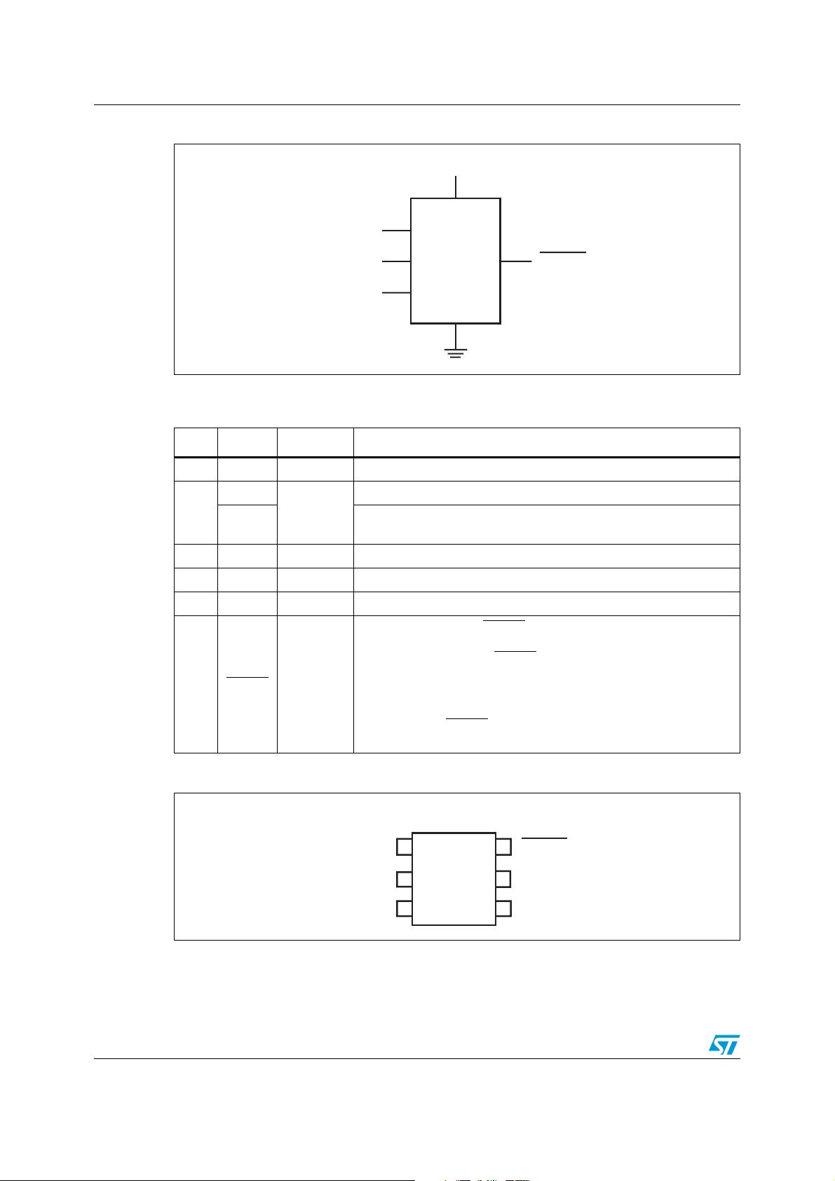
Figure 1. Logic diagram
V2IN / V
CC
V1IN
(1)
V3IN
STM6700
RESET
STM6710
V4IN
1. Open drain
Table 2. Signal names
Pin Name Type Function (STM6710 / STM6700)
1 V1IN Input Input voltage 1
V2IN
2
V
3 V3IN Input Input voltage 3
Input/supply
CC
Input voltage 2 and device power supply pin
For the triple monitor voltage STM6700 and for STM6710Q, this pin
is the V
supply pin and it is not monitored
CC
AM04617v1
4 V4IN Input Input voltage 4
5 GND Supply Ground
6 RESET
Output
Active low, open drain RESET
input drops below the specified threshold. Once all inputs rise above
their threshold voltages, RESET
(STM6710) before going high.
For the triple monitor (STM6700) it remains low for 5 µs
(propagation delay - no t
The open drain RESET
(STM6710) or V
(STM6700/STM6710Q).
CC
output. Output goes low when any
remains low for typical 200 ms
).
REC
has a weak (10 µA) internal pull-up to V2IN
Figure 2. Pinout SOT23-6
SOT23-6
(1)
AM04618v1
1. Open drain
V1IN
V2IN (V
CC
V3IN
)
1
STM6700
2
STM6710
3
6
5
4
RESET
GND
V4IN
Note: For the STM6700 and STM6710Q, pin 2 is a fixed VCC, thereby making it a triple voltage
reset, while the STM6710 is a quad voltage reset.
6/21 Doc ID 16887 Rev 2
STM6700, STM6710 Description
Pin descriptions
V1IN, V3IN,V4IN (VxIN)
The VxIN pins are used for nominal input voltages for 1.8 V, 2.5 V and 5.0 V supplies. The
voltage at this pin is compared against an internal factory-programmed voltage trip point,
Vrst.
RESET
is first asserted low when the device is initially powered and VxIN < 1 V and then at
any time thereafter when VxIN falls below Vrst. The device is designed with typical
hysteresis of 0.3% with respect to its threshold to help prevent oscillation due to noise and is
immune to brief power supply transients.
V2IN
The V2IN is used to power the STM6710 device. In normal operations V2IN is also
monitored. For STM6710Q and STM6700 variations this pin is the V
power supply but is
CC
not monitored.
Ground (VSS)
This pin (GND) is the ground pin for the power supply and is tied to VSS.
RESET
The RESET output is an open drain output that asserts low whenever a monitored supply
falls below the minimum threshold. STM6710 provides an extended reset timeout period of
typically 200 ms.
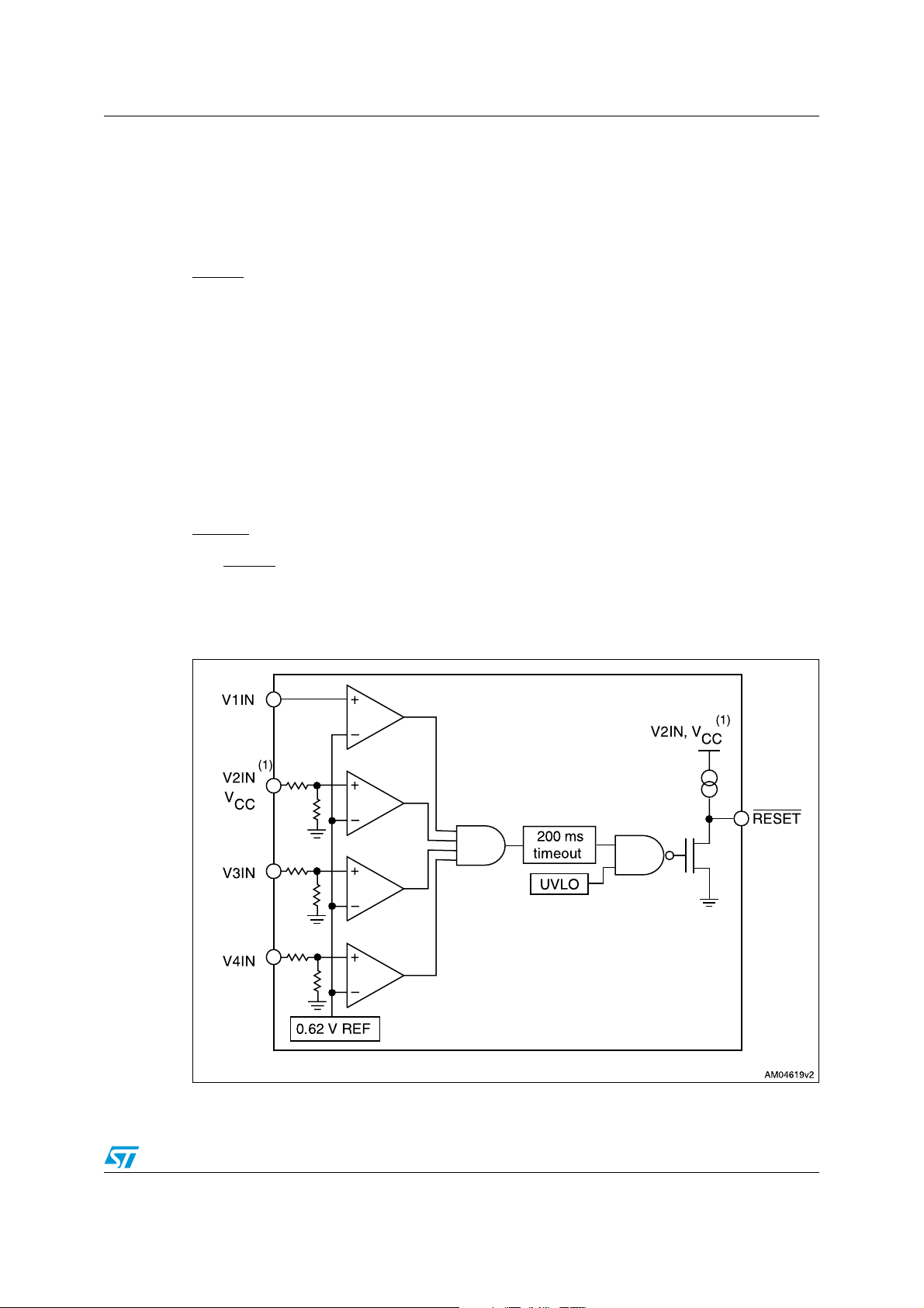
Figure 3. Functional block diagram
1. The STM6700 and STM6710Q are powered via the V2IN input which is the supply voltage. When this pin is
V
, the input is not monitored.
CC
Doc ID 16887 Rev 2 7/21
 Loading...