

Smart push-button on/off controller with Smart Reset™ and
Features
■ Operating voltage 1.6 V to 5.5 V
■ Low standby current of 0.6 µA
■ Adjustable Smart Reset
driven by external C
■ Power-up duration determined primarily by
push-button press (STM6600) or by fixed time
period, t
■ Debounced PB and SR inputs
■ PB and SR ESD inputs withstand voltage up to
ON_BLANK
±15 kV (air discharge) ±8 kV (contact
discharge)
■ Active high or active low enable output option
(EN
or EN) provides control of MOSFET,
DC-DC converter, regulator, etc.
■ Secure startup, interrupt, Smart Reset
power-down driven by push-button
■ Precise 1.5 V voltage reference with 1%
accuracy
■ Industrial operating temperature –40 to +85 °C
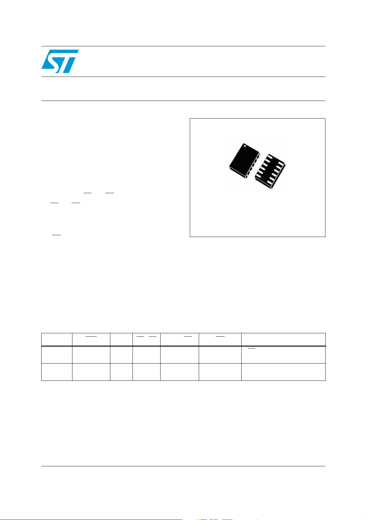
■ Available in TDFN12 2 x 3 mm package
™
assertion delay time
SRD
(STM6601)
™
or
STM6600, STM6601
power-on lockout
Datasheet − production data
TDFN12
Applications
■ Portable devices
■ Termin
■
A
■ Cell phones and smart phones
■ PDAs, palmtops, organizers
als
udio and video players
Table 1. Device summary
Device RST C
STM6600 open drain
STM6601 open drain
1. External pull-up resistor needs to be connected to open drain outputs.
2. For a successful startup, the PS
(1)
(1)
June 2012 Doc ID 15453 Rev 11 1/52
This is information on a product in full production.
PB / SR EN or EN INT Startup process
SRD
PB must be held low until the
✓✓push-pull open drain
✓✓push-pull open drain
(Power Supply Hold) needs to be pulled high within specific time, t
HOLD
(1)
(1)
PS
HOLD
PB can be released before the
PS
HOLD
(2)
confirmation
(2)
confirmation
ON_BLANK
.
www.st.com
1

Contents STM6600, STM6601
Contents
1 Description . . . . . . . . . . . . . . . . . . . . . . . . . . . . . . . . . . . . . . . . . . . . . . . . . 5
2 Pin descriptions . . . . . . . . . . . . . . . . . . . . . . . . . . . . . . . . . . . . . . . . . . . . 9
3 Operation . . . . . . . . . . . . . . . . . . . . . . . . . . . . . . . . . . . . . . . . . . . . . . . . . 12
4 Waveforms . . . . . . . . . . . . . . . . . . . . . . . . . . . . . . . . . . . . . . . . . . . . . . . . 14
5 Typical operating characteristics . . . . . . . . . . . . . . . . . . . . . . . . . . . . . 28
6 Maximum ratings . . . . . . . . . . . . . . . . . . . . . . . . . . . . . . . . . . . . . . . . . . . 38
7 DC and AC characteristics . . . . . . . . . . . . . . . . . . . . . . . . . . . . . . . . . . . 39
8 Package mechanical data . . . . . . . . . . . . . . . . . . . . . . . . . . . . . . . . . . . . 42
9 Part numbering . . . . . . . . . . . . . . . . . . . . . . . . . . . . . . . . . . . . . . . . . . . . 46
10 Product selector . . . . . . . . . . . . . . . . . . . . . . . . . . . . . . . . . . . . . . . . . . . 49
11 Revision history . . . . . . . . . . . . . . . . . . . . . . . . . . . . . . . . . . . . . . . . . . . 51
2/52 Doc ID 15453 Rev 11

STM6600, STM6601 List of tables
List of tables
Table 1. Device summary. . . . . . . . . . . . . . . . . . . . . . . . . . . . . . . . . . . . . . . . . . . . . . . . . . . . . . . . . . 1
Table 2. Pin descriptions . . . . . . . . . . . . . . . . . . . . . . . . . . . . . . . . . . . . . . . . . . . . . . . . . . . . . . . . . . 7
Table 3. Absolute maximum ratings . . . . . . . . . . . . . . . . . . . . . . . . . . . . . . . . . . . . . . . . . . . . . . . . . 38
Table 4. Operating and AC measurement conditions . . . . . . . . . . . . . . . . . . . . . . . . . . . . . . . . . . . . 39
Table 5. DC and AC characteristics . . . . . . . . . . . . . . . . . . . . . . . . . . . . . . . . . . . . . . . . . . . . . . . . . 39
Table 6. TDFN12 (2 x 3 mm) package mechanical data . . . . . . . . . . . . . . . . . . . . . . . . . . . . . . . . . 43
Table 7. Carrier tape dimensions for TDFN12 (2 x 3 mm) package . . . . . . . . . . . . . . . . . . . . . . . . . 45
Table 8. STM6600 ordering information scheme . . . . . . . . . . . . . . . . . . . . . . . . . . . . . . . . . . . . . . . 46
Table 9. STM6601 ordering information scheme . . . . . . . . . . . . . . . . . . . . . . . . . . . . . . . . . . . . . . . 48
Table 10. STM6600 product selector . . . . . . . . . . . . . . . . . . . . . . . . . . . . . . . . . . . . . . . . . . . . . . . . . 49
Table 11. STM6601 product selector . . . . . . . . . . . . . . . . . . . . . . . . . . . . . . . . . . . . . . . . . . . . . . . . . 50
Table 12. Document revision history . . . . . . . . . . . . . . . . . . . . . . . . . . . . . . . . . . . . . . . . . . . . . . . . . 51
Doc ID 15453 Rev 11 3/52

List of figures STM6600, STM6601
List of figures
Figure 1. Application hookup . . . . . . . . . . . . . . . . . . . . . . . . . . . . . . . . . . . . . . . . . . . . . . . . . . . . . . . 5
Figure 2. Basic functionality (option with enable deassertion after long push) . . . . . . . . . . . . . . . . . . 6
Figure 3. Basic functionality (option with RST
Figure 4. Logic diagram . . . . . . . . . . . . . . . . . . . . . . . . . . . . . . . . . . . . . . . . . . . . . . . . . . . . . . . . . . . . 6
Figure 5. TDFN12 pin connections . . . . . . . . . . . . . . . . . . . . . . . . . . . . . . . . . . . . . . . . . . . . . . . . . . . 7
Figure 6. Block diagram . . . . . . . . . . . . . . . . . . . . . . . . . . . . . . . . . . . . . . . . . . . . . . . . . . . . . . . . . . . . 8
Figure 7. Successful power-up on STM6600 (PB
Figure 8. Successful power-up on STM6600 (t
Figure 9. Unsuccessful power-up on STM6600 (PB
Figure 10. Unsuccessful power-up on STM6600 (t
Figure 11. Successful power-up on STM6601. . . . . . . . . . . . . . . . . . . . . . . . . . . . . . . . . . . . . . . . . . . 18
Figure 12. Unsuccessful power-up on STM6601
Figure 13. Power-up on STM660x with voltage dropout . . . . . . . . . . . . . . . . . . . . . . . . . . . . . . . . . . . 20
Figure 14. PB
Figure 15. Long push, PB
Figure 16. Long push, SR
interrupt. . . . . . . . . . . . . . . . . . . . . . . . . . . . . . . . . . . . . . . . . . . . . . . . . . . . . . . . . . . . . 21
pressed first . . . . . . . . . . . . . . . . . . . . . . . . . . . . . . . . . . . . . . . . . . . . . . . . 22
pressed first . . . . . . . . . . . . . . . . . . . . . . . . . . . . . . . . . . . . . . . . . . . . . . . . 22
Figure 17. Invalid long push . . . . . . . . . . . . . . . . . . . . . . . . . . . . . . . . . . . . . . . . . . . . . . . . . . . . . . . . 23
Figure 18. Long push (option with RST
assertion). . . . . . . . . . . . . . . . . . . . . . . . . . . . . . . . . . . . . . . . 24
Figure 19. Long push (option with enable deassertion) . . . . . . . . . . . . . . . . . . . . . . . . . . . . . . . . . . . 25
Figure 20. Undervoltage detected for <t
Figure 21. Undervoltage detected for >t
Figure 22. PB
output waveform . . . . . . . . . . . . . . . . . . . . . . . . . . . . . . . . . . . . . . . . . . . . . . . . . . . 27
OUT
SRD
SRD
Figure 23. Supply current vs. temperature, normal state. . . . . . . . . . . . . . . . . . . . . . . . . . . . . . . . . . . 28
Figure 24. Supply current vs. temperature, standby state . . . . . . . . . . . . . . . . . . . . . . . . . . . . . . . . . . 28
Figure 25. Supply current vs. supply voltage, normal state . . . . . . . . . . . . . . . . . . . . . . . . . . . . . . . . . 29
Figure 26. Supply current vs. supply voltage, standby state . . . . . . . . . . . . . . . . . . . . . . . . . . . . . . . . 29
Figure 27. Threshold vs. temperature, V
Figure 28. Threshold hysteresis vs. temperature, V
Figure 29. Debounce period vs. supply voltage . . . . . . . . . . . . . . . . . . . . . . . . . . . . . . . . . . . . . . . . . . 31
Figure 30. C
charging current vs. temperature, VCC = 3.6 V . . . . . . . . . . . . . . . . . . . . . . . . . . . . . 31
SRD
Figure 31. Output low voltage vs. output low current, T
Figure 32. Output high voltage vs. output high current, T
Figure 33. Output voltage vs. supply voltage, I
Figure 34. Input voltage vs. temperature . . . . . . . . . . . . . . . . . . . . . . . . . . . . . . . . . . . . . . . . . . . . . . . 33
Figure 35. Reference output voltage vs. temperature, V
Figure 36. Reference output voltage vs. load current, V
Figure 37. Reference output voltage vs. supply voltage, T
Figure 38. Reference startup, I
= 15 µF, TA = 25 °C . . . . . . . . . . . . . . . . . . . . . . . . . . . . . . . . . . . 35
REF
Figure 39. Reference response to steps on supply voltage, I
Figure 40. Reference response to steps in load current, V
Figure 41. TDFN12 (2 x 3 mm) package outline . . . . . . . . . . . . . . . . . . . . . . . . . . . . . . . . . . . . . . . . . 43
Figure 42. TDFN12 (2 x 3 mm) recommended footprint . . . . . . . . . . . . . . . . . . . . . . . . . . . . . . . . . . . 44
Figure 43. Carrier tape for TDFN12 (2 x 3 mm) package . . . . . . . . . . . . . . . . . . . . . . . . . . . . . . . . . . 45
assertion after long push) . . . . . . . . . . . . . . . . . . . . . . 6
released prior to t
ON_BLANK
expires prior to PB release) . . . . . . . . . . . 15
released prior to t
ON_BLANK
. . . . . . . . . . . . . . . . . . . . . . . . . . . . . . . . . . . . . . . . . . . . . . . . . . . . 19
expires prior to PB release) . . . . . . . . . 17
ON_BLANK
ON_BLANK
expiration) . . . . . . . . 14
) . . . . . . . . . . . . . . 16
. . . . . . . . . . . . . . . . . . . . . . . . . . . . . . . . . . . . . . . . . . . . 26
. . . . . . . . . . . . . . . . . . . . . . . . . . . . . . . . . . . . . . . . . . . . 26
= 3.4 V (typ.) . . . . . . . . . . . . . . . . . . . . . . . . . . . . . . . . . 30
TH+
OUT
= 200 mV (typ.) . . . . . . . . . . . . . . . . . . . . . . 30
HYST
= 25 °C . . . . . . . . . . . . . . . . . . . . . . . . . . . . 32
A
= 25 °C. . . . . . . . . . . . . . . . . . . . . . . . . . . 32
A
= 1 mA, TA = 25 °C . . . . . . . . . . . . . . . . . . . . . . . 33
= 2.0 V. . . . . . . . . . . . . . . . . . . . . . . . . . . 34
CC
= 2.0 V, TA = 25 °C . . . . . . . . . . . . . . . . . 34
CC
= 25 °C. . . . . . . . . . . . . . . . . . . . . . . . . . 35
A
= 15 µA, TA = 25 °C . . . . . . . . . . . . 36
REF
= 3.6 V, TA = 25 °C . . . . . . . . . . . . . . . 37
CC
4/52 Doc ID 15453 Rev 11
STM6600, STM6601 Description
1 Description
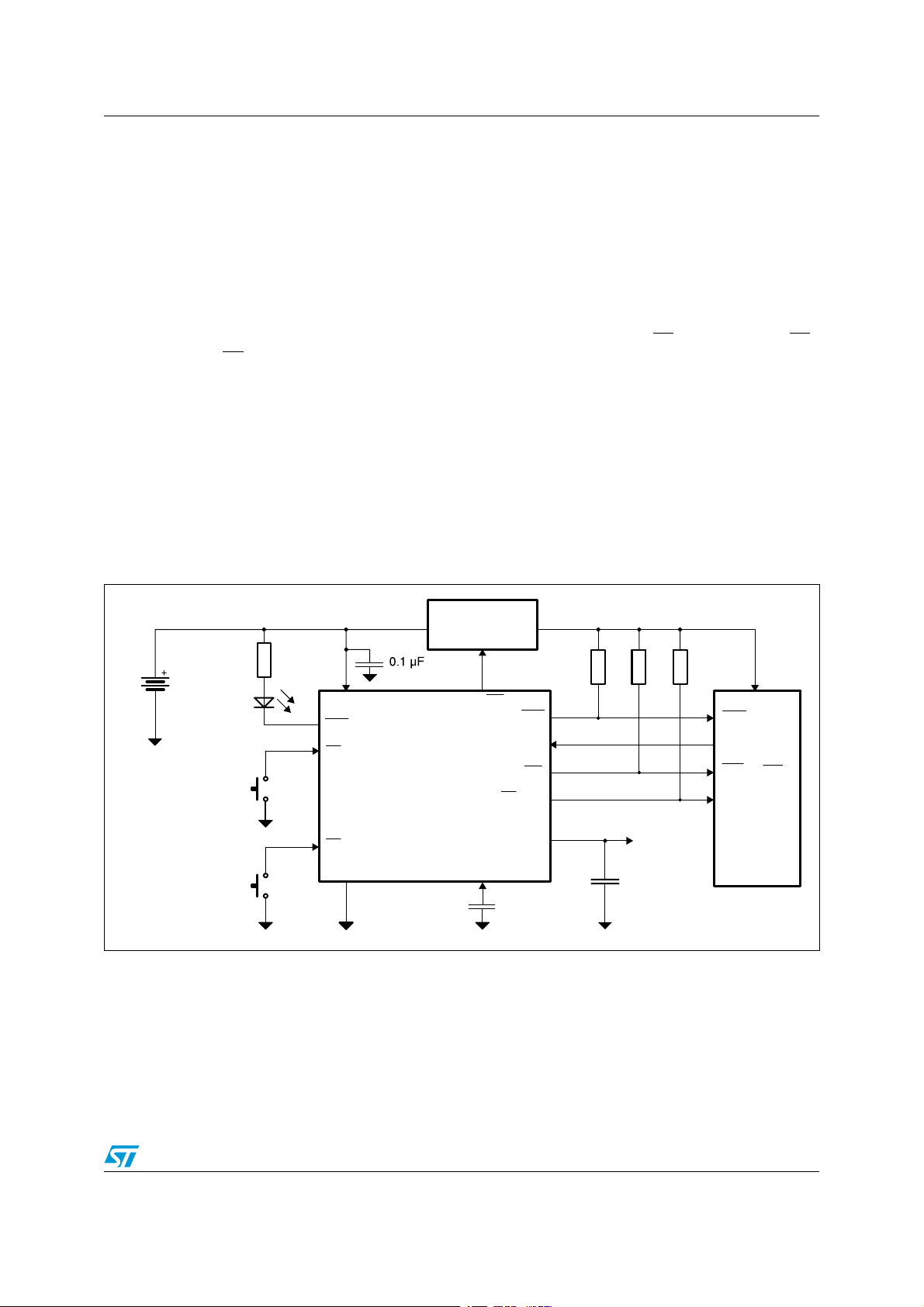
The STM6600-01 devices monitor the state of connected push-button(s) as well as sufficient
supply voltage. An enable output controls power for the application through the MOSFET
transistor, DC-DC converter, regulator, etc. If the supply voltage is above a precise voltage
threshold, the enable output can be asserted by a simple press of the button. Factoryselectable supply voltage thresholds are determined by highly accurate and temperaturecompensated references. An interrupt is asserted by pressing the push-button during
normal operation and can be used to request a system power-down. The interrupt is also
asserted if undervoltage is detected. By a long push of one button (PB
and SR
) either a reset is asserted or power for the application is disabled depending on the
option used.
The device also offers additional features such as precise 1.5 V voltage reference with very
tight accuracy of 1%, separate output indicating undervoltage detection and separate output
for distinguishing between interrupt by push-button or undervoltage.
The device consumes very low current of 6 µA during normal operation and only 0.6 µA
current during standby.
The STM6600-01 is available in the TDFN12 package and is offered in several options
among features such as selectable threshold, hysteresis, timeouts, output types, etc.
) or two buttons (PB
Figure 1. Application hookup
$#$#CONVERTER
$#$#CONVERTER
POWER-/3&%4
POWER-/3&%4
REGULATORETC
REGULATORETC
2
2
#
#
2
2
2%&
2%&
2
2
6
,%$
,%$
1. A resistor is required for open drain output type only. A 10 kΩ pull-up is sufficient in most applications.
2. Capacitor C
3. For the STM6601 the processor has to confirm the proper power-on during the fixed time period, t
feature prevents the user from turning on the system when there is a faulty power switch or an unresponsive
microprocessor.
is mandatory on V
REF
6
##
##
6##
6##
,/
,/
0"
0"
32
32
'.$
'.$
output (even if V
REF
34-
34-
34-
34-
%.%.
%.%.
#
#
is not used). Capacitor value of 1 µF is recommended.
REF
03
03
32$
32$
(/,$
(/,$
0"
0"
6
6
#
#
32$
32$
234
234
).4
).4
/54
/54
2%&
2%&
2
2
ON_BLANK
6
6
$$
$$
234
234
)/
)/
.-)OR).4
.-)OR).4
)/
)/
-#5
-#5
#05
#05
"!3%"!.$
"!3%"!.$
!-V
!-V
. This failsafe
Doc ID 15453 Rev 11 5/52
Description STM6600, STM6601
Figure 2. Basic functionality (option with enable deassertion after long push)
POWER-UP
(1)
INTERRUPT
(short push)
POWER-DOWN
(long push)
PB
SR
EN
INT interrupt interrupt
1. For power-up the battery voltage has to be above V
threshold.
TH+
Figure 3. Basic functionality (option with RST assertion after long push)
PB
SR
POWER-UP
(1)
INTERRUPT
(short push)
POWER-DOWN
(long push)
AM00243v1
RST
INT interrupt interrupt
1. For power-up the battery voltage has to be above V
Figure 4. Logic diagram
V
PB
SR
PS
HOLD
C
SRD
STM6600
STM6601
GND
TH+
CC
threshold.
EN (EN)
RST
INT
PB
VCC
V
REF
AM00243bv1
OUT
LO
AM00236v1
6/52 Doc ID 15453 Rev 11
STM6600, STM6601 Description
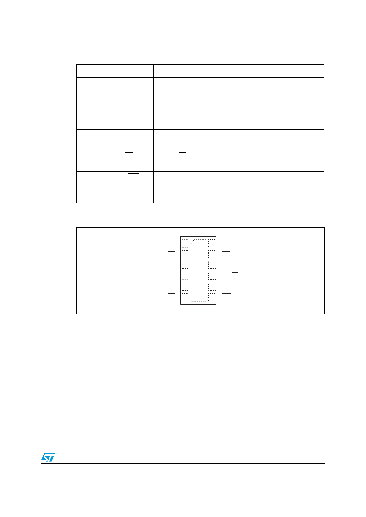
Table 2. Pin descriptions
Pin number Symbol Function
1V
CC
2SR
3V
4PS
5C
REF
HOLD
SRD
6PB
7VCC
8PB
LO
OUT
9EN or EN
10 RST
11 INT
Power supply input
Smart Reset™ button input
Precise 1.5 V voltage reference
PS
HOLD
input
Adjustable Smart Reset™ delay time input
Push-button input
Output for high threshold comparator output (V
Status of PB push-button input
Enable output
Reset output
Interrupt output
12 GND Ground
Figure 5. TDFN12 pin connections
V
CC
SR
V
REF
PS
HOLD
C
SRD
PB
1
2
3
4
5
67
12
11
10
9
8
GND
INT
RST
EN (EN)
PB
OUT
VCC
LO
TH+
)
AM00245v1
Doc ID 15453 Rev 11 7/52
Description STM6600, STM6601
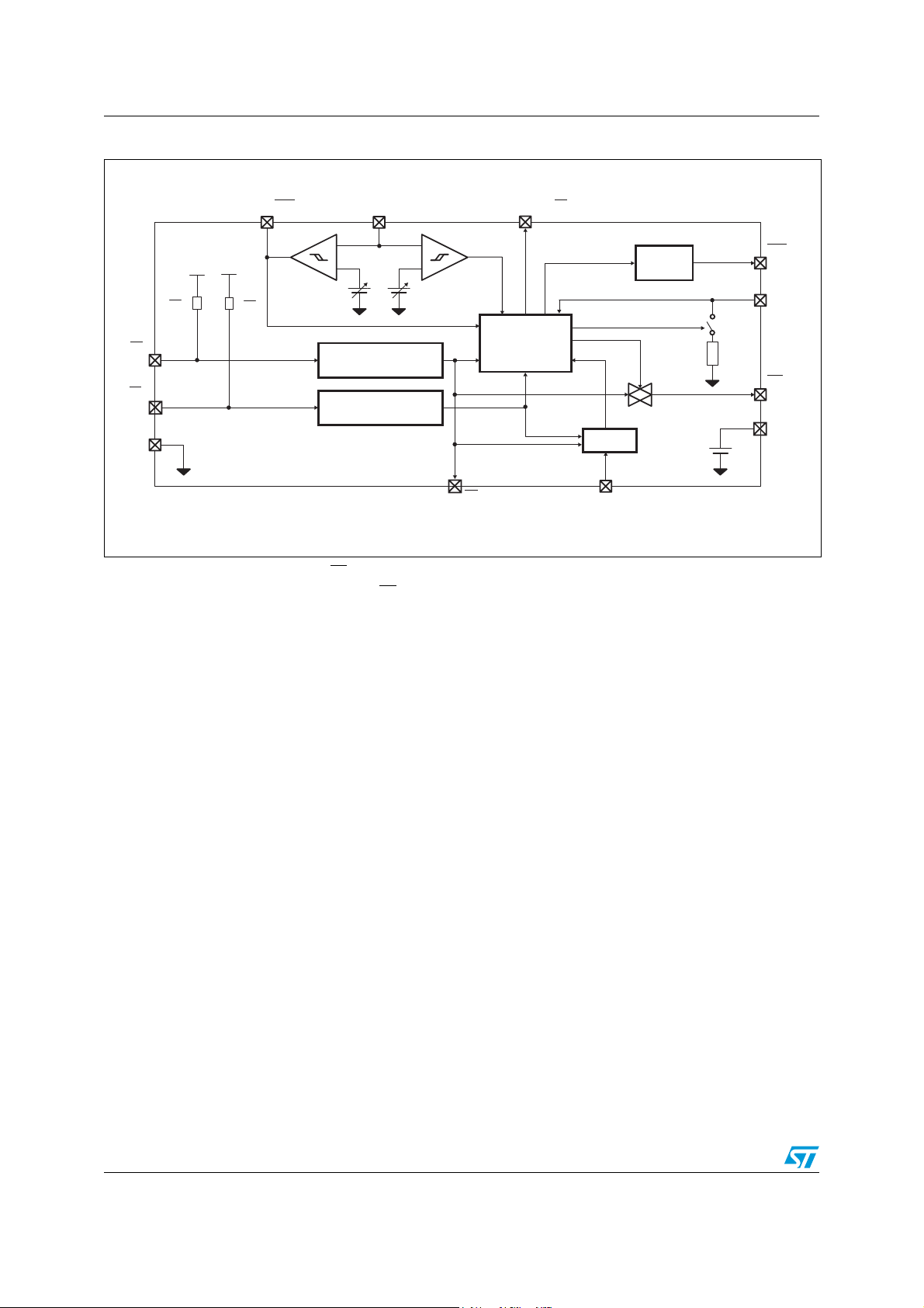
Figure 6. Block diagram
VCC
LO
+
V
V
CC
CC
(1)
R
PB
(2)
R
SR
V
–
TH+
V
CC
+
–
V
TH–
EN (EN)
Smart
PB
SR
GND
Glitch immunity
Edge detector debounce
Glitch immunity
Edge detector debounce
PB
logic
OUT
1. Internal pull-up resistor connected to PB input (see Table 5 for precise specifications).
2. Optional internal pull-up resistor connected to SR
device options).
3. Internal pull-down resistor is connected to PS
input (see Table 5 for precise specifications and Table 10 for detailed
input only during startup (see Figure 7, 8, 9, 10, 11, 12, 13, and 18).
HOLD
SRD logic
C
SRD
t
REC
generator
R
PSHOLD
RST
PS
HOLD
(3)
INT
V
REF
1.5 V
AM00237v3
8/52 Doc ID 15453 Rev 11

STM6600, STM6601 Pin descriptions
2 Pin descriptions
VCC - power supply input
is monitored during startup and normal operation for sufficient voltage level. Decouple
V
CC
the V
SR
This input is equipped with voltage detector with a factory-trimmed threshold and has ±8 kV
HBM ESD protection.
pin from ground by placing a 0.1 µF capacitor as close to the device as possible.
CC
- Smart Reset™ button input
Both PB
and SR buttons have to be pressed and held for t
period so the long push is
SRD
recognized and the reset is asserted (or the enable output is deasserted depending on the
option) - see Figure 15, 16, and 17.
Active low SR
input is usually connected to GND through the momentary push-button (see
Figure 1) and it has an optional 100 kΩ pull-up resistor. It is also possible to drive this input
using an external device with either open drain (recommended) or push-pull output. Open
drain output can be connected in parallel with push-button or other open drain outputs,
which is not possible with push-pull output. S
R input is monitored for falling edge after
power-up and must not be grounded permanently.
- external precise 1.5 V voltage reference
V
REF
This 1.5 V voltage reference is specified with very tight accuracy of 1% (see Table 5). It has
proper output voltage as soon as the reset output is deasserted (i.e. after t
expires) and
REC
it is disabled when the device enters standby mode. A mandatory capacitor needs to be
connected to V
output (even if V
REF
is not used). Capacitor value of 1 µF is
REF
recommended.
HOLD
input
PS
This input is equipped with a voltage detector with a factory-trimmed threshold. It is used to
confirm correct power-up of the device (if EN or EN
(if EN or EN
Forcing PS
is asserted).
high during power-up confirms the proper start of the application and keeps
HOLD
is not asserted) or to initiate a shutdown
enable output asserted. Because most processors have outputs in high-Z state before
initialization, an internal pull-down resistor is connected to PS
input during startup (see
HOLD
Figure 7, 8, 9, 10, 11, 12, 13, and 18).
Forcing the PS
signal low during normal operation deasserts the enable output (see
HOLD
Figure 14). Input voltage on this pin is compared to an accurate voltage reference.
- Smart Reset™ delay time input
C
SRD
A capacitor to ground determines the additional time (t
pressed and held before a long push is recognized. The connected C
charged with I
the C
capacitor reaches the V
SRD
current. Additional Smart Reset™ delay time t
SRD
voltage threshold. It is recommended to use a low
SRD
ESR capacitor (e.g. ceramic). If the capacitor is not used, leave the C
capacitor is connected, there is no t
and a long push is recognized right after t
SRD
) that PB with SR must be
SRD
SRD
capacitor is
SRD
ends when voltage on
pin open. If no
SRD
expires (see Figure 18 and 19).
Doc ID 15453 Rev 11 9/52
INT_Min

Pin descriptions STM6600, STM6601
PB - power ON switch
This input is equipped with a voltage detector with a factory-trimmed threshold and has
± 8 kV HBM ESD protection.
When the PB
asserted if the battery voltage is above the threshold V
button is pressed and held, the battery voltage is detected and EN (or EN) is
during the whole t
TH+
DEBOUNCE
period (see Figure 13).
A short push of the push-button during normal operation can initiate an interrupt through
debounced INT
either assert reset output RST
output (see Figure 14) and a long push of PB and SR simultaneously can
(see Figure 18) or deassert the EN or EN output (see
Figure 19) based on the option used.
Note: A switch to GND must be connected to this input (e.g. mechanical push-button, open drain
output of external circuitry, etc.), see Figure 1. This ensures a proper startup signal on PB
(i.e. a transition from full V
below specified VIL). PB input has an internal 100 kΩ pull-up
CC
resistor connected.
VCC
During power-up, VCC
successful power-up (i.e. during normal operation) VCC
- high threshold detection output
LO
is low when VCC supply voltage is below the V
LO
threshold. After
is low anytime undervoltage is
LO
TH+
detected (see Figure 13).
Output type is active low and open drain by default. Open drain output type requires a pullup resistor. A 10 kΩ is sufficient in most applications.
VCC
PB
If the push-button PB
If PB
t
deasserted (see Figure 22). PB
At startup on the STM6601 PB
assertion will be ignored until t
is floating when STM660x is in standby mode.
LO
- PB input state
OUT
is pressed, the pin stays low during the t
is asserted for the entire t
. If PB is asserted after t
INT_Min
DEBOUNCE
INT_Min
OUT
OUT
ON_BLANK
expire s, PB
ignores PB assertion during an undervoltage condition.
will respond only to the first PB assertion and any other
time period.
period, PB
OUT
DEBOUNCE
will then stay low for at least
OUT
will return high as soon as PB is
expires. This output is active low and open drain by
default. Open drain output type requires a pull-up resistor. A 10 kΩ is sufficient in most
applications.
10/52 Doc ID 15453 Rev 11

STM6600, STM6601 Pin descriptions
EN or EN - enable output
This output is intended to enable system power (see Figure 1). EN is asserted high after
a valid turn-on event has been detected and confirmed (i.e. push-button has been pressed
and held for t
DEBOUNCE
or more and V
CC
> V
voltage level has been detected - see
TH+
Figure 13). EN is released low if any of the conditions below occur:
a) the push-button is released before PS
Figure 9) or t
ON_BLANK
expires before PS
is driven high (valid for STM6600, see
HOLD
is driven high during startup (valid
HOLD
for both STM6600 and STM6601, see Figure 10 and 12).
b) PS
c) an undervoltage condition is detected for more than t
is driven low during normal operation (see Figure 14).
HOLD
SRD
+ t
INT_Min
+ t
DEBOUNCE
(see Figure 21).
d) a long push of the buttons is detected (only for the device with option “EN
deasserted by long push” - see Figure 19) or PS
t
ON_BLANK
after a long push of the buttons (only for the device with option “RST
is not driven high during
HOLD
asserted by long push” - see Figure 18).
Described logic levels are inverted in case of EN
- reset output
RST
This output pulls low for t
a) during startup. PB
for at least t
DEBOUNCE
:
REC
has been pressed (falling edge on the PB detected) and held
and VCC > V
output. Output type is push-pull by default.
(see Figure 7, 8, 9, 10, 11, 12 and 13 for
TH+
more details).
b) after long push detection (valid only for the device with option “RST
long push”). PB
more than t
by the external capacitor C
has been pressed (falling edge on the PB detected) and held for
DEBOUNCE
+ t
(additional Smart Reset™ delay time can be adjusted
SRD
) - see Figure 18.
SRD
asserted by
Output type is active low and open drain by default. Open drain output type requires a pullup resistor. A 10 kΩ is sufficient in most applications.
- interrupt output
INT
While the system is under normal operation (PS
asserted), the INT
a) V
CC
is driven low if:
falls below V
threshold (i.e. undervoltage is detected - see Figure 20 and
TH-
is driven high, power for application is
HOLD
21).
b) the falling edge on the PB
more. INT
INT
The state of the PB
either the assertion of the PB
on V
INT
.
CC
output is asserted low for at least t
is driven low after t
signal is held high during power-up.
output can be used to determine if the interrupt was caused by
OUT
input, or was due to the detection of an undervoltage condition
is detected and the push-button is held for t
DEBOUNCE
INT_Min
and stays low as long as PB is held. The
.
DEBOUNCE
or
Output type is active low and open drain by default. Open drain output type requires a pullup resistor. A 10 kΩ is sufficient in most applications.
GND - ground
Doc ID 15453 Rev 11 11/52

Operation STM6600, STM6601
3 Operation
The STM6600-STM6601 simplified smart push-button on/off controller with Smart Reset™
and power-on lockout enables and disables power for the application depending on pushbutton states, signals from the processor, and battery voltage.
Power-on
Because most of the processors have outputs in high-Z state before initialization, an internal
pull-down resistor is connected to PS
12, 13, and 18).
To power up the device the push-button PB
V
has to be above V
CC
below V
V
TH+
during the t
TH+
(see Figure 13). After t
goes low), reset output RST
for the whole t
TH+
DEBOUNCE
DEBOUNCE
is asserted for t
, the counter is reset and starts to count again when V
by the processor. During initialization, the processor sets the PS
On the STM6600 the PS
t
ON_BLANK
expiration, otherwise the enable signal is deasserted (EN goes low, EN goes
signal has to be set high prior to push-button release and
HOLD
high) - see Figure 7, 8, 9, and 10. The time up to push-button release represents the
maximum time allowed for the system to power up and initialize the circuits driving the
PS
input. If the PS
HOLD
signal is low at push-button release, the enable output is
HOLD
deasserted immediately, thus turning off the system power. If t
push-button release, the PS
state is checked at its expiration. This safety feature
HOLD
disables the power and prevents discharging the battery if the push-button is stuck or it is
held for an unreasonable period of time and the application is not responding (see Figure 8
and 10). PB
status, INT status and VCC undervoltage detection are not monitored until
power-up is completed.
input during startup (see Figure 7, 8, 9, 10, 11,
HOLD
has to be pressed for at least t
DEBOUNCE
period. If the battery voltage drops
DEBOUNCE
the enable signal is asserted (EN goes high, EN
and then the startup routine is performed
REC
ON_BLANK
signal high.
HOLD
expires prior to
and
CC
>
On the STM6601 the PS
signal has to be set high before t
HOLD
ON_BLANK
the enable signal is deasserted - see Figure 11 and 12. In this case the t
expires, otherwise
ON_BLANK
period is
the maximum time allowed for the power switch and processor to perform the proper poweron. If the PS
released immediately, thus turning off the system power. PB
undervoltage detection are not monitored during the entire t
signal is low at the end of the blanking period, the enable output is
HOLD
status, INT status and VCC
ON_BLANK
period. This failsafe
feature prevents the user from turning on the system when there is a faulty power switch or
an unresponsive microprocessor.
Push-button interrupt
If the device works under normal operation (i.e. PS
pressed for more than t
generated on the INT
NMI
) a safeguard routine can be performed and the power can be shut down by setting
PS
low - see Figure 14.
HOLD
DEBOUNCE
output. By connecting INT to the processor interrupt input (INT or
, a negative pulse with minimum t
is high) and the push-button PB is
HOLD
INT_Min
width is
Forced power-down mode
The PS
output can be forced low anytime during normal operation by the processor
HOLD
and can deassert the enable signal - see Figure 14.
Undervoltage detection
voltage drops below V
If V
CC
voltage threshold during normal operation, the INT output is
TH-
driven low (see Figure 20 and Figure 21).
12/52 Doc ID 15453 Rev 11

STM6600, STM6601 Operation
If an undervoltage condition is detected for t
DEBOUNCE
+ t
INT_Min
+ t
, the enable output is
SRD
deasserted (see Figure 21).
Hardware reset or power-down while system not responding
If the system is not responding and the system hangs, the PB
pressed simultaneously longer than t
a) either the reset output RST
only for the device with option “RST
b) or the power is disabled by EN or EN
DEBOUNCE
is asserted for t
+ t
INT_Min
REC
asserted by long push”) – see Figure 18
signal (valid only for the device with option
and SR push-buttons can be
+ t
, and then
SRD
and the processor is reset (valid
“EN deasserted by long push”) – see Figure 19
The t
is set by the external capacitor connected to the C
SRD
pin. SR input is monitored
SRD
for falling edge after power-up and must not be grounded permanently.
Standby
If the enable output is deasserted (i.e. EN is low or EN
standby mode with low current consumption (see Ta bl e 5). In standby mode PB
is high), the STM660x device enters
input is only
monitored for the falling edge. The external 1.5 V voltage reference is also disabled in
standby mode.
Doc ID 15453 Rev 11 13/52
Waveforms STM6600, STM6601
4 Waveforms
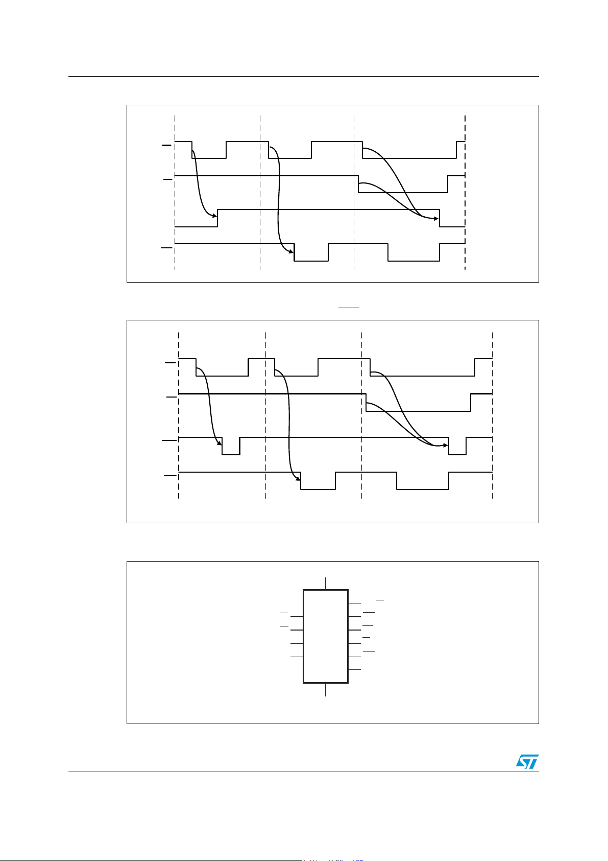
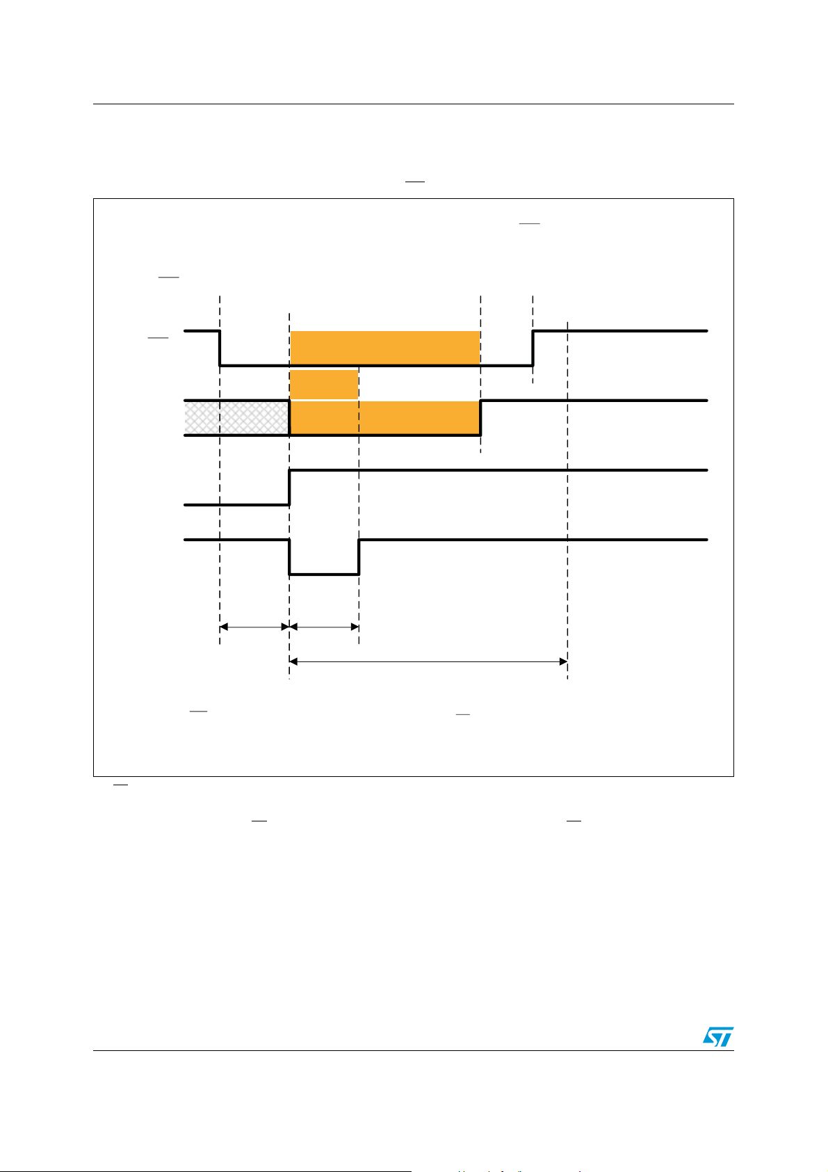
Figure 7. Successful power-up on STM6600 (PB released prior to t
PB released prior to t
expiration
Push-button pressed and
PB connected to GND
(1)
PB
sets PS
undervoltage detection
V
CC
ignored
HOLD
PS
processor
HOLD
PS
EN remains asserted
ignored
PS
HOLD
EN
(2)
(3)
internal pull-down resistor
connected to PS
HOLD
input
RST
ON_BLANK
HOLD
expiration)
state detected as high
ON_BLANK
t
DEBOUNCE
Note:
INT signal is held high during power-up (i.e. until PB release in this case).
V
is considered VCC > V
CC
1. PB detection on falling and rising edges.
2. Internal pull-down resistor 300 kΩ is connected to PS
3. EN signal is high even after PB
release, because processor sets PS
t
REC
TH+
.
t
ON_BLANK
input during power-up.
HOLD
HOLD
AM00247v3
signal high before PB is released.
14/52 Doc ID 15453 Rev 11
STM6600, STM6601 Waveforms
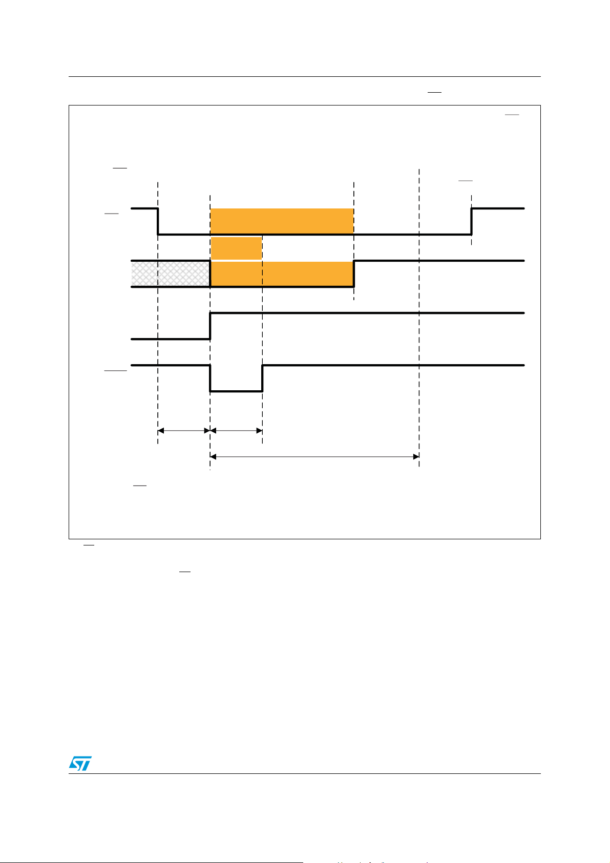
Figure 8. Successful power-up on STM6600 (t
Push-button pressed and
PB connected to GND
undervoltage detection
PB
(1)
V
PS
CC
HOLD
ignored
ignored
PS
HOLD
EN
(2)
(3)
internal pull-down resistor
connected to PS
RST
ON_BLANK
processor
sets PS
input
HOLD
expires prior to PB release)
t
ON_BLANK
expired prior to PB
release
PS
state detected as high
HOLD
EN remains asserted
HOLD
PB released
t
DEBOUNCE
Note:
INT signal is held high during power-up (i.e. until t
V
is considered VCC > V
CC
1. PB detection on falling and rising edges.
2. Internal pull-down resistor 300 kΩ is connected to PS
3. t
ON_BLANK
expires prior to PB release so PS
t
REC
.
TH+
is checked at its expiration.
HOLD
t
ON_BLANK
input during power-up.
HOLD
ON_BLANK
expires in this case).
AM00247bv2
Doc ID 15453 Rev 11 15/52
Waveforms STM6600, STM6601
Figure 9. Unsuccessful power-up on STM6600 (PB released prior to t
PB released
Push-button pressed and
PB connected to GND
(1)
PB
undervoltage detection
V
CC
ignored
HOLD
PS
PS
EN deasserted
state detected as low
HOLD
ignored
PS
HOLD
EN
(2)
(3)
internal pull-down resistor
connected to PS
HOLD
input
RST
ON_BLANK
PB status
ignored
)
t
DEBOUNCE
Note:
INT signal is held high during power-up (i.e. until PB release in this case).
V
is considered VCC > V
CC
1. PB detection on falling and rising edges.
2. Internal pull-down resistor 300 kΩ is connected to PS
3. EN signal goes low with PB
release, because processor did not force PS
TH+
t
REC
.
t
ON_BLANK
input during power-up.
HOLD
signal high.
HOLD
t
EN_OFF
AM00248v3
16/52 Doc ID 15453 Rev 11
 Loading...