

ST STM6510 User Manual

STM6510
Dual push-button Smart ResetTM with capacitor-adjustable delays
Features
■ Dual Smart Reset™ push-button inputs with
capacitor-adjustable extended reset setup
delay (t
■ Capacitor-adjustable reset pulse duration
(t
REC
■ Power-on reset
–RST
■ Factory-programmable thresholds to monitor
V
CC
■ Operating voltage 1.0 V (active-low output
valid) to 5.5 V
■ Low supply current (1.4 µA)
■ Operating temperature: industrial grade –40 °C
to +85 °C
■ TDFN8 package: 2 mm x 2 mm x 0.75 mm
■ RoHS compliant
)
SRC
)
active-low, open-drain
in the range of 1.575 to 4.625 V typ.
TDFN8 (DG)
2 mm x 2 mm
Applications
■ Mobile phones, smartphones
■ e-books
■ MP3 players
■ Games
■ Portable navigation devices
■ Any application that requires delayed reset
push-button(s) response for improved system
stability
February 2010 Doc ID 16788 Rev 2 1/26
www.st.com
1

Contents STM6510
Contents
1 Description . . . . . . . . . . . . . . . . . . . . . . . . . . . . . . . . . . . . . . . . . . . . . . . . . 5
1.1 Smart Reset™ devices . . . . . . . . . . . . . . . . . . . . . . . . . . . . . . . . . . . . . . . 5
1.2 STM6510 . . . . . . . . . . . . . . . . . . . . . . . . . . . . . . . . . . . . . . . . . . . . . . . . . . 5
1.3 Pin descriptions . . . . . . . . . . . . . . . . . . . . . . . . . . . . . . . . . . . . . . . . . . . . . 9
1.3.1 Power supply (VCC) . . . . . . . . . . . . . . . . . . . . . . . . . . . . . . . . . . . . . . . . . 9
1.3.2 Ground (V
1.3.3 Smart Reset™ push-button inputs (SR0
1.3.4 Adjustable delay of Smart Reset™ input (SRC pin) . . . . . . . . . . . . . . . . 9
1.3.5 Reset output (RST
1.3.6 Adjustable reset timeout (TREC
2 Typical operating characteristics . . . . . . . . . . . . . . . . . . . . . . . . . . . . . 11
) . . . . . . . . . . . . . . . . . . . . . . . . . . . . . . . . . . . . . . . . . . . . . . 9
SS
, SR1) . . . . . . . . . . . . . . . . . . . . 9
) . . . . . . . . . . . . . . . . . . . . . . . . . . . . . . . . . . . . . . . . 10
pin) . . . . . . . . . . . . . . . . . . . . . . . . 10
ADJ
3 Maximum ratings . . . . . . . . . . . . . . . . . . . . . . . . . . . . . . . . . . . . . . . . . . . 13
4 DC and AC parameters . . . . . . . . . . . . . . . . . . . . . . . . . . . . . . . . . . . . . . 14
5 Package mechanical data . . . . . . . . . . . . . . . . . . . . . . . . . . . . . . . . . . . . 17
6 Part numbering . . . . . . . . . . . . . . . . . . . . . . . . . . . . . . . . . . . . . . . . . . . . 23
7 Package marking . . . . . . . . . . . . . . . . . . . . . . . . . . . . . . . . . . . . . . . . . . . 24
8 Revision history . . . . . . . . . . . . . . . . . . . . . . . . . . . . . . . . . . . . . . . . . . . 25
2/26 Doc ID 16788 Rev 2

STM6510 List of tables
List of tables
Table 1. Signal names . . . . . . . . . . . . . . . . . . . . . . . . . . . . . . . . . . . . . . . . . . . . . . . . . . . . . . . . . . . . 6
Table 2. tSRC programmed by an ideal external capacitor . . . . . . . . . . . . . . . . . . . . . . . . . . . . . . . . 9
Table 3. tREC programmed by an ideal external capacitor . . . . . . . . . . . . . . . . . . . . . . . . . . . . . . . 10
Table 4. Absolute maximum ratings . . . . . . . . . . . . . . . . . . . . . . . . . . . . . . . . . . . . . . . . . . . . . . . . . 13
Table 5. Operating and measurement conditions . . . . . . . . . . . . . . . . . . . . . . . . . . . . . . . . . . . . . . . 14
Table 6. DC and AC characteristics . . . . . . . . . . . . . . . . . . . . . . . . . . . . . . . . . . . . . . . . . . . . . . . . . 15
Table 7. Possible VCC voltage thresholds . . . . . . . . . . . . . . . . . . . . . . . . . . . . . . . . . . . . . . . . . . . . 16
Table 8. TDFN – 8-lead 2 x 2 x 0.75 mm, 0.5 mm pitch package mechanical data . . . . . . . . . . . . . 18
Table 9. Parameter for landing pattern - TDFN – 8-lead 2 x 2 mm package . . . . . . . . . . . . . . . . . . 19
Table 10. Carrier tape dimensions . . . . . . . . . . . . . . . . . . . . . . . . . . . . . . . . . . . . . . . . . . . . . . . . . . . 20
Table 11. Reel dimensions . . . . . . . . . . . . . . . . . . . . . . . . . . . . . . . . . . . . . . . . . . . . . . . . . . . . . . . . . 21
Table 12. Ordering information scheme . . . . . . . . . . . . . . . . . . . . . . . . . . . . . . . . . . . . . . . . . . . . . . . 23
Table 13. Package marking . . . . . . . . . . . . . . . . . . . . . . . . . . . . . . . . . . . . . . . . . . . . . . . . . . . . . . . . 24
Table 14. Document revision history . . . . . . . . . . . . . . . . . . . . . . . . . . . . . . . . . . . . . . . . . . . . . . . . . 25
Doc ID 16788 Rev 2 3/26

List of figures STM6510
List of figures
Figure 1. Logic diagram . . . . . . . . . . . . . . . . . . . . . . . . . . . . . . . . . . . . . . . . . . . . . . . . . . . . . . . . . . . . 6
Figure 2. Pin connections . . . . . . . . . . . . . . . . . . . . . . . . . . . . . . . . . . . . . . . . . . . . . . . . . . . . . . . . . . 6
Figure 3. Block diagram . . . . . . . . . . . . . . . . . . . . . . . . . . . . . . . . . . . . . . . . . . . . . . . . . . . . . . . . . . . . 7
Figure 4. Single-button Smart Reset™ typical hookup . . . . . . . . . . . . . . . . . . . . . . . . . . . . . . . . . . . . 8
Figure 5. Dual-button Smart Reset™ typical hookup. . . . . . . . . . . . . . . . . . . . . . . . . . . . . . . . . . . . . . 8
Figure 6. Timing waveforms. . . . . . . . . . . . . . . . . . . . . . . . . . . . . . . . . . . . . . . . . . . . . . . . . . . . . . . . . 9
Figure 7. Supply current (I
Figure 8. Smart Reset™ delay (t
Figure 9. Reset timeout period (t
Figure 10. Reset threshold (V
Figure 11. AC testing input/output waveforms . . . . . . . . . . . . . . . . . . . . . . . . . . . . . . . . . . . . . . . . . . . 14
Figure 12. TDFN – 8-lead 2 x 2 x 0.75 mm, 0.5 mm pitch package outline . . . . . . . . . . . . . . . . . . . . . 18
Figure 13. Landing pattern - TDFN – 8-lead 2 x 2 mm without thermal pad . . . . . . . . . . . . . . . . . . . . 19
Figure 14. Carrier tape . . . . . . . . . . . . . . . . . . . . . . . . . . . . . . . . . . . . . . . . . . . . . . . . . . . . . . . . . . . . 20
Figure 15. Reel dimensions . . . . . . . . . . . . . . . . . . . . . . . . . . . . . . . . . . . . . . . . . . . . . . . . . . . . . . . . . 21
Figure 16. Tape trailer/leader. . . . . . . . . . . . . . . . . . . . . . . . . . . . . . . . . . . . . . . . . . . . . . . . . . . . . . . . 22
Figure 17. Pin 1 orientation . . . . . . . . . . . . . . . . . . . . . . . . . . . . . . . . . . . . . . . . . . . . . . . . . . . . . . . . . 22
Figure 18. Package marking, top view . . . . . . . . . . . . . . . . . . . . . . . . . . . . . . . . . . . . . . . . . . . . . . . . . 24
) vs. temperature . . . . . . . . . . . . . . . . . . . . . . . . . . . . . . . . . . . . . . . . . 11
CC
RST
) vs. temperature, C
SRC
) vs. temperature, C
REC
= 0.56 µF . . . . . . . . . . . . . . . . . . . . . . 11
SRC
= 0.01 µF . . . . . . . . . . . . . . . . . . . . . 12
tREC
) vs. temperature, “S” threshold option, VCC falling. . . . . . . . . . . . . 12
4/26 Doc ID 16788 Rev 2

STM6510 Description
1 Description
1.1 Smart Reset™ devices
The Smart Reset™ device family STM65xx provides a useful feature that ensures
inadvertent short reset push-button closures do not cause system resets. This is done by
implementing an extended Smart Reset™ input delay (t
input levels and setup delay are met, the device generates an output reset pulse with userprogrammable timeout period (t
REC
).
The typical application hookup shows that the dual Smart Reset™ inputs can be also
connected to the applications interrupt to allow the control of both the interrupt pin and the
hard reset functions. If the push-buttons are closed for a short time, the processor is only
interrupted. If the system still does not respond properly, holding the push-buttons for the
extended setup time (t
) causes a hard reset of the processor through the reset output.
SRC
The Smart Reset™ feature helps significantly increase system stability.
The STM65xx family of Smart Reset™ devices consists of low-current microprocessor reset
circuits targeted at applications such as MP3 players, portable navigation devices or mobile
phones, generally any application that requires delayed reset push-button(s) response for
improved system stability. The STM65xx devices feature single or dual Smart Reset™
inputs (SRx). The delayed Smart Reset™ setup time (t
adding an external capacitor on the SRC pin or selectable by three-state logic. The delayed
setup period ignores switch closures shorter than t
SRC
The STM65xx devices have active-low (optionally active-high) open-drain reset (RST
output(s) with or without an internal pull-up resistor or push-pull as output options, with or
without the power-on reset function.
). Once the valid Smart Reset™
SRC
) options are adjustable by
SRC
, thus preventing undesired resets.
)
Some devices also have an undervoltage monitoring feature: the reset output is also
asserted when the monitored supply voltage V
reset output remains asserted for the reset timeout period (t
voltage goes above the specified threshold.
1.2 STM6510
The STM6510 has two combined Smart Reset™ inputs (SR0 and SR1) with Smart Reset™
setup delay (t
STM6510 feature is adjustable output reset pulse time t
(C
).
tREC
Additionally, the V
reset output goes active and remains active while V
defined duration of the reset pulse t
drops below the specified threshold. The
CC
) programmed by an external capacitor on the SRC pin. An additional
SRC
REC
is monitored and if it drops below the selected V
CC
REC
.
is below the V
CC
) after the monitored supply
REC
by adding an external capacitor
threshold, the
RST
threshold, plus the
RST
Doc ID 16788 Rev 2 5/26
Description STM6510
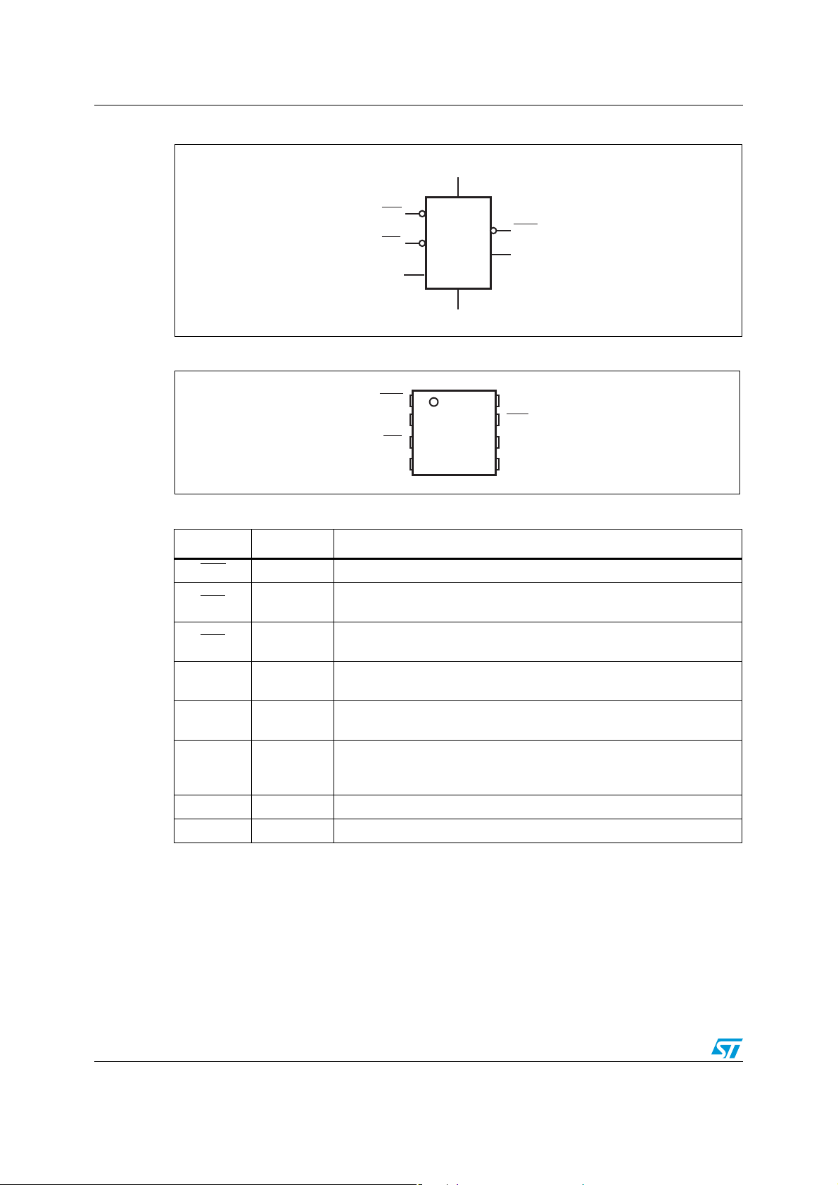
Figure 1. Logic diagram
V
CC
SR0
SR1
SRC
STM6510
V
SS
RST
TREC
ADJ
AM00389a
Figure 2. Pin connections
STM
6510
8
V
CC
7
SR0
6
TREC
ADJ
5
SRC
Table 1. Signal names
RST
V
SS
SR1
NC
1
2
3
4
Symbol Input/output Description
RST
SR0 Input
SR1 Input
SRC Input
TREC
ADJ
Output Reset output, active-low (open-drain).
Primary push-button Smart Reset™ input. Active-low, internal 65 kΩ
pull-up resistor to V
CC
.
Secondary push-button Smart Reset™ input. Active-low, internal 65 kΩ
pull-up resistor to V
CC
.
Smart Reset™ input delay setup control. Connect an external capacitor
to this pin to adjust the delay setup time (t
Input
Input pin for t
capacitor (C
reset pulse duration adjustment. Connect an external
REC
) to this pin to determine t
tREC
Supply voltage input. Power supply for the device and an input for the
V
CC
Supply
monitored supply voltage. A 0.1 µF decoupling ceramic capacitor is
recommended to be connected between V
V
SS
Supply Ground
NC No connect (not bonded); should be connected to V
).
SRC
.
REC
and VSS pins.
CC
AM00390
SS.
6/26 Doc ID 16788 Rev 2

STM6510 Description
Figure 3. Block diagram
V
CC
65 kΩ 65 kΩ
V
RST
COMPARE
t
REC
generator
RST
SR0
SR1
SRC
Logic
TREC
C
ADJ
tREC
AM00391a
Doc ID 16788 Rev 2 7/26

Description STM6510
Figure 4. Single-button Smart Reset™ typical hookup
V
CC
100 kΩ
C
RESET
SRC
INT/
NMI
PUSH-BUTTON
SWITCH
C
tREC
TREC
ADJ
STM6510
V
CC
RST
SRC
SR1
V
SR0
SS
Note: When only one Smart Reset™ input push-button is used, tie both the SR
Figure 5. Dual-button Smart Reset™ typical hookup
V
CC
V
CC
MCU
V
SS
AM04870v1
inputs together.
V
CC
RST
SS
SRC
SR1
SR0
C
SRC
PUSH-BUTTON
SWITCH
C
tREC
TREC
ADJ
STM6510
V
8/26 Doc ID 16788 Rev 2
100 kΩ
RESET
INT/
NMI
PUSH-BUTTON
SWITCH
V
CC
MCU
V
SS
AM004871v1
 Loading...