

STM6502, STM6503
STM6504, STM6505
Dual push-button Smart ResetTM with user-adjustable setup delays
Features
■ Dual Smart Reset push-button inputs with
extended reset setup delay
■ Adjustable Smart Reset setup delay (t
by external capacitor or three-state logic
(product options): t
■ Power-on reset
■ Single RST output, active-low, open-drain
■ Factory-programmable thresholds to monitor
V
in the range of 1.575 to 4.625 V typ.
CC
■ Operating voltage 1.0 V (active-low output
= 2, 6, 10 s (min.)
SRC
valid) to 5.5 V
■ Low supply current
■ Operating temperature:
industrial grade –40 °C to +85 °C
■ TDFN8 package: 2 mm x 2 mm x 0.75 mm
■ RoHS compliant
SRC
):
TDFN8 (DG)
2 mm x 2 mm
Applications
■ Mobile phones, smartphones
■ e-books
■ MP3 players
■ Games
■ Portable navigation devices
■ Any application that requires delayed reset
push-button(s) response for improved system
stability
Table 1. Device summary
t
Voltage inputs Smart Reset inputs
Part
number
V
STM6502
STM6503 ✓✓✓ ✓✓TDFN-8L
STM6504
STM6505 ✓✓ ✓ ✓ ✓ ✓ ✓TDFN-8L
1. Contact local ST sales office for availability.
February 2011 Doc ID 16101 Rev 6 1/29
(1)
(1)
V
CC
✓✓✓ ✓ ✓TDFN-8L
✓✓ ✓ ✓✓TDFN-8L
BAT
SR0 SR1
SRE
immediate,
independent
SRC pin
SRC
programming
Three-
Ext.
state
input
TSR
Reset or Power
Good outputs
RST
BLD
Package
www.st.com
1

Contents STM6502, STM6503, STM6504, STM6505
Contents
1 Description . . . . . . . . . . . . . . . . . . . . . . . . . . . . . . . . . . . . . . . . . . . . . . . . . 5
1.1 Smart Reset devices . . . . . . . . . . . . . . . . . . . . . . . . . . . . . . . . . . . . . . . . . 5
1.2 Pin descriptions . . . . . . . . . . . . . . . . . . . . . . . . . . . . . . . . . . . . . . . . . . . . 10
1.2.1 Power supply (VCC) . . . . . . . . . . . . . . . . . . . . . . . . . . . . . . . . . . . . . . . . 10
1.2.2 Ground (V
1.2.3 Primary Smart Reset input (SR0
1.2.4 Secondary Smart Reset input (SR1
1.2.5 Edge-triggered Smart Reset input (SRE pin) – STM6504 only . . . . . . . 11
1.2.6 Adjustable delay of Smart Reset input (SRC pin) – STM6502
and STM6505 only . . . . . . . . . . . . . . . . . . . . . . . . . . . . . . . . . . . . . . . . . 11
1.2.7 Programmable Smart Reset input delay (TSR pin) – STM6503
and STM6504 only . . . . . . . . . . . . . . . . . . . . . . . . . . . . . . . . . . . . . . . . . 12
1.2.8 Reset output (RST
1.2.9 Battery monitoring input (V
1.2.10 Battery low detect output (BLD
) . . . . . . . . . . . . . . . . . . . . . . . . . . . . . . . . . . . . . . . . . . . . . 10
SS
) . . . . . . . . . . . . . . . . . . . . . . . . . . . . . 10
) . . . . . . . . . . . . . . . . . . . . . . . . . . . 10
) . . . . . . . . . . . . . . . . . . . . . . . . . . . . . . . . . . . . . . . . 12
) – STM6505 only . . . . . . . . . . . . . . . . . 12
BAT
) – STM6505 only . . . . . . . . . . . . . . . . . 12
2 Typical operating characteristics . . . . . . . . . . . . . . . . . . . . . . . . . . . . . 13
3 Maximum ratings . . . . . . . . . . . . . . . . . . . . . . . . . . . . . . . . . . . . . . . . . . . 15
4 DC and AC parameters . . . . . . . . . . . . . . . . . . . . . . . . . . . . . . . . . . . . . . 16
5 Package mechanical data . . . . . . . . . . . . . . . . . . . . . . . . . . . . . . . . . . . . 20
6 Part numbering . . . . . . . . . . . . . . . . . . . . . . . . . . . . . . . . . . . . . . . . . . . . 26
7 Package marking . . . . . . . . . . . . . . . . . . . . . . . . . . . . . . . . . . . . . . . . . . . 27
8 Revision history . . . . . . . . . . . . . . . . . . . . . . . . . . . . . . . . . . . . . . . . . . . 28
2/29 Doc ID 16101 Rev 6

STM6502, STM6503, STM6504, STM6505 List of tables
List of tables
Table 1. Device summary. . . . . . . . . . . . . . . . . . . . . . . . . . . . . . . . . . . . . . . . . . . . . . . . . . . . . . . . . . 1
Table 2. Signal names . . . . . . . . . . . . . . . . . . . . . . . . . . . . . . . . . . . . . . . . . . . . . . . . . . . . . . . . . . . . 7
Table 3. t
Table 4. Absolute maximum ratings . . . . . . . . . . . . . . . . . . . . . . . . . . . . . . . . . . . . . . . . . . . . . . . . . 15
Table 5. Operating and measurement conditions. . . . . . . . . . . . . . . . . . . . . . . . . . . . . . . . . . . . . . . 16
Table 6. DC and AC characteristics . . . . . . . . . . . . . . . . . . . . . . . . . . . . . . . . . . . . . . . . . . . . . . . . . 17
Table 7. V
Table 8. TDFN – 8-lead 2 x 2 x 0.75 mm, 0.5 mm pitch package mechanical data . . . . . . . . . . . . . 21
Table 9. Parameter for landing pattern - TDFN – 8-lead 2 x 2 mm package . . . . . . . . . . . . . . . . . . 22
Table 10. Carrier tape dimensions . . . . . . . . . . . . . . . . . . . . . . . . . . . . . . . . . . . . . . . . . . . . . . . . . . . 23
Table 11. Reel dimensions . . . . . . . . . . . . . . . . . . . . . . . . . . . . . . . . . . . . . . . . . . . . . . . . . . . . . . . . . 24
Table 12. Ordering information scheme . . . . . . . . . . . . . . . . . . . . . . . . . . . . . . . . . . . . . . . . . . . . . . . 26
Table 13. Package marking . . . . . . . . . . . . . . . . . . . . . . . . . . . . . . . . . . . . . . . . . . . . . . . . . . . . . . . . 27
Table 14. Document revision history . . . . . . . . . . . . . . . . . . . . . . . . . . . . . . . . . . . . . . . . . . . . . . . . . 28
programmed by an ideal external capacitor – STM6502 and STM6505 . . . . . . . . . . 11
SRC
voltage thresholds . . . . . . . . . . . . . . . . . . . . . . . . . . . . . . . . . . . . . . . . . . . . . . . . . . . . 19
CC
Doc ID 16101 Rev 6 3/29

STM6502, STM6503, STM6504, STM6505 List of figures
List of figures
Figure 1. Logic diagrams . . . . . . . . . . . . . . . . . . . . . . . . . . . . . . . . . . . . . . . . . . . . . . . . . . . . . . . . . . . 6
Figure 2. Pin connections . . . . . . . . . . . . . . . . . . . . . . . . . . . . . . . . . . . . . . . . . . . . . . . . . . . . . . . . . . 6
Figure 3. Block diagram - STM6502, STM6503, STM6504 . . . . . . . . . . . . . . . . . . . . . . . . . . . . . . . . . 8
Figure 4. Block diagram - STM6505 . . . . . . . . . . . . . . . . . . . . . . . . . . . . . . . . . . . . . . . . . . . . . . . . . . 8
Figure 5. Single-button Smart Reset typical hookup . . . . . . . . . . . . . . . . . . . . . . . . . . . . . . . . . . . . . . 9
Figure 6. Dual-button Smart Reset typical hookup . . . . . . . . . . . . . . . . . . . . . . . . . . . . . . . . . . . . . . . 9
Figure 7. STM6502, STM6503 timing . . . . . . . . . . . . . . . . . . . . . . . . . . . . . . . . . . . . . . . . . . . . . . . . 10
Figure 8. STM6504 timing . . . . . . . . . . . . . . . . . . . . . . . . . . . . . . . . . . . . . . . . . . . . . . . . . . . . . . . . . 11
Figure 9. STM6505 timing . . . . . . . . . . . . . . . . . . . . . . . . . . . . . . . . . . . . . . . . . . . . . . . . . . . . . . . . . 12
Figure 10. Supply current (I
Figure 11. Smart Reset delay (t
Figure 12. Reset threshold (V
Figure 13. V
monitoring threshold (V
BAT
Figure 14. AC testing input/output waveforms . . . . . . . . . . . . . . . . . . . . . . . . . . . . . . . . . . . . . . . . . . . 16
Figure 15. TDFN – 8-lead 2 x 2 x 0.75 mm, 0.5 mm pitch package outline. . . . . . . . . . . . . . . . . . . . . 21
Figure 16. Landing pattern - TDFN – 8-lead 2 x 2 mm without thermal pad . . . . . . . . . . . . . . . . . . . . 22
Figure 17. Carrier tape . . . . . . . . . . . . . . . . . . . . . . . . . . . . . . . . . . . . . . . . . . . . . . . . . . . . . . . . . . . . 23
Figure 18. Reel dimensions . . . . . . . . . . . . . . . . . . . . . . . . . . . . . . . . . . . . . . . . . . . . . . . . . . . . . . . . . 24
Figure 19. Tape trailer/leader. . . . . . . . . . . . . . . . . . . . . . . . . . . . . . . . . . . . . . . . . . . . . . . . . . . . . . . . 25
Figure 20. Pin 1 orientation . . . . . . . . . . . . . . . . . . . . . . . . . . . . . . . . . . . . . . . . . . . . . . . . . . . . . . . . . 25
Figure 21. Package marking, top view. . . . . . . . . . . . . . . . . . . . . . . . . . . . . . . . . . . . . . . . . . . . . . . . . 27
) vs. temperature (STM6505) . . . . . . . . . . . . . . . . . . . . . . . . . . . . . . . . 13
CC
) vs. temperature, C
SRC
) vs. temperature, “S” threshold option, VCC falling (STM6505) . . . 14
RST
BATTH)
vs. temperature, falling (STM6505) . . . . . . . . . . . . . . 14
= 0.62 µF (STM6505) . . . . . . . . . . . . . . 13
SRC
Doc ID 16101 Rev 6 4/29

STM6502, STM6503, STM6504, STM6505 Description
1 Description
STM6502 has two combined Smart Reset inputs (SR0 and SR1) with delayed Smart Reset
setup time (t
STM6503 is similar to STM6502, has two combined delayed Smart Reset inputs (SR0
and three user-selectable delayed Smart Reset setup time (t
s through a three-state TSR input pin: when connected to ground, t
open, t
SRC
STM6504 has two independent Smart Reset inputs. SR0
setup time (t
input pin: when connected to ground, t
connected to V
is edge-triggered with a special debounce time (t
edge after a valid reset period.
) programmed by an external capacitor on the SRC pin.
SRC
= 6 s; when connected to VCC, t
= 10 s (all the times are minimum).
SRC
provides the delayed Smart Reset
) function with three user-selectable t
SRC
CC
, t
= 10 s (all the times are minimum). SRE provides instant reset. SRE
SRC
= 2 s; when left open, t
SRC
DEBOUNCE
options through a three-state TSR
SRC
, SR1)
) options of 2 s, 6 s and 10
SRC
= 2 s; when left
SRC
= 6 s; when
SRC
= 240 ms min.) at the falling
STM6505 has two combined delayed Smart Reset inputs (SR0
adjustable reset delay setup time via an external capacitor connected to the SRC pin.
The RST
output depends also on the VCC monitoring threshold. STM6505 also provides
independent low battery detect (BLD
voltage V
detect output pin (BLD
BAT
. V
is monitored for low voltage and provides an indication on the battery low
BAT
). V
BAT
be used to set the actual battery voltage threshold. V
(16 mV max.). V
V
pin; VCC must be ≥ 1.575 V for proper operation of the V
CC
is voltage monitoring input only, the device is powered only from the
BAT
1.1 Smart Reset devices
The Smart Reset device family STM65xx provides a useful feature that ensures inadvertent
short reset push-button closures do not cause system resets. This is done by implementing
extended Smart Reset input delay (t
delay are met, the device generates an output reset pulse with user-programmable timeout
period (t
The Smart Reset inputs can be also connected to the applications interrupt to allow the
control of both the interrupt pin and the hard reset functions. If the push-buttons are closed
for a short time, the processor is only interrupted. If the system still does not respond
properly, holding the push-buttons for the extended setup time (t
the processor through the reset outputs. The Smart Reset feature helps significantly
increase system stability.
REC
).
, SR1) and provides an
) output controlled by the secondary external input
threshold is 1.25 V, fixed, and an external resistor divider is to
threshold hysteresis is 8 mV typ.
BAT
comparator.
BAT
). Once the valid Smart Reset input levels and setup
SRC
) causes hard reset of
SRC
The STM65xx family of Smart Reset devices consists of low current microprocessor reset
circuits targeted at applications such as MP3 players, navigation, smartphones or mobile
phones; generally any application that requires delayed reset push-button(s) response for
improved system stability. The STM65xx devices feature single or dual Smart Reset inputs
(SR). The delayed Smart Reset setup time (t
) options of 2 s, 6 s and 10 s (all min.) are
SRC
adjustable by an external capacitor on the SRC pin or selectable by three-state logic. The
delayed setup period ignores switch closures shorter than t
, thus preventing unwanted
SRC
resets.
Doc ID 16101 Rev 6 5/29
Description STM6502, STM6503, STM6504, STM6505
The STM65xx devices have active-low (optionally active-high) open-drain reset (RST)
output(s) with or without internal pull-up resistor or push-pull as output options, with factoryprogrammed or capacitor-adjustable or push-buttons defined output reset pulse duration,
with or without power-on reset function.
Some devices also have an undervoltage monitoring feature: the reset output is also
asserted when the monitored supply voltage V
reset output remains asserted for the reset timeout period (t
drops below the specified threshold. The
CC
) after the monitored supply
REC
voltage goes above the specified threshold.
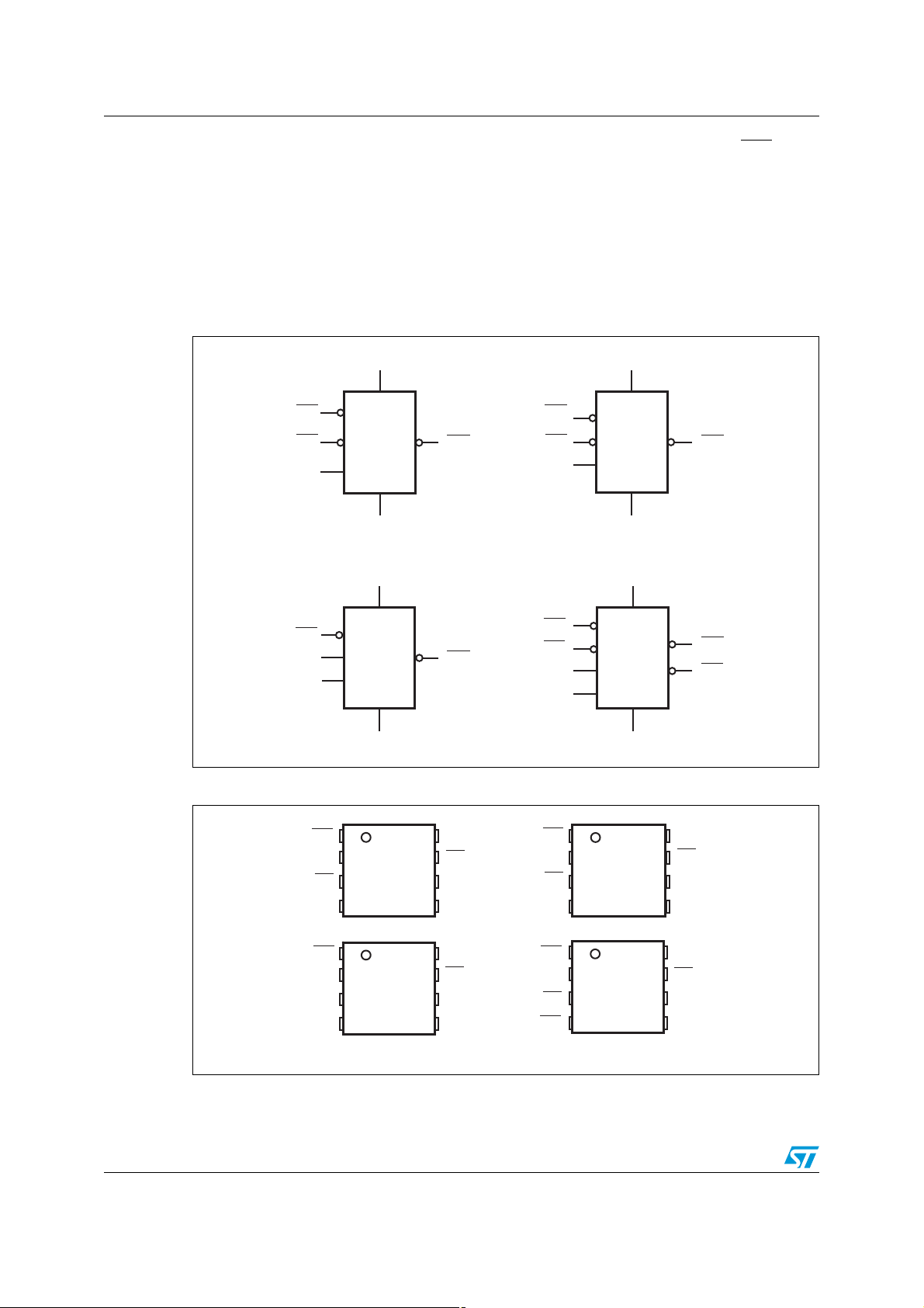
Figure 1. Logic diagrams
V
CC
SR0
SR1
SRC
SR0
SRE
TSR
STM6502
V
SS
V
CC
STM6504
V
SS
Figure 2. Pin connections
RST
RST
SR0
SR1
TSR
SR0
SR1
SRC
V
BAT
V
CC
STM6503
V
SS
V
CC
STM6505
V
SS
RST
RST
BLD
AM00378
8
1
RST
V
2
SS
SR1
NC NC
RST
V
SS
SRE
NC
STM
6502
3
4
1
2
STM
6504
3
4
V
CC
7
SR0
6
SRC
5
8
V
CC
7
SR0
6
TSR
5
NC
6/29 Doc ID 16101 Rev 6
1
RST
V
2
SS
SR1
NC NC
RST
V
SS
SR1
BLD
STM
6503
3
4
1
2
STM
6505
3
4
8
7
6
5
8
7
6
5
V
SR0
TSR
V
CC
SR0
SRC
V
BAT
CC
AM00379
STM6502, STM6503, STM6504, STM6505 Description
Table 2. Signal names
Symbol
RST
BLD
SR0
Input/
output
Description
Output Open-drain reset output, active-low.
Output Battery low detect output, active-low, open-drain. STM6505 only.
Input
Primary push-button Smart Reset input. Active-low, with or without internal
65 kΩ pull-up to V
(product options).
CC
Secondary push-button Smart Reset input - combines with the primary push-
SR1
Input
button reset to provide setup delay time before reset. Active-low, with or without
internal 65 kΩ pull-up to V
(product options).
CC
Secondary push-button Smart Reset input - provides instant Smart Reset. SRE
SRE Input
is edge-triggered with a special debounce time (t
the falling edge after a valid reset period. Active-high, no internal pull-up to V
STM6504 only.
SRC Input
Smart Reset input delay setup control: connect to an external capacitor to adjust
the delay setup time (t
). STM6502 and STM6505 only.
SRC
A three-state Smart Reset input delay setup control. When connected to
TSR Input
ground, t
t
= 10 s (all times are minimum). TSR is a DC-type input, intended to be
SRC
either permanently grounded, permanently connected to V
= 2 s; when left open, t
SRC
= 6 s; when connected to VCC,
SRC
left open. If left open, for improved system glitch immunity it is strongly
recommended to connect a 0.1 µF decoupling ceramic capacitor between the
TSR and V
pins. STM6503 and STM6504 only.
SS
Supply voltage input. Power supply for the device and an input for the monitored
V
V
BAT
V
Supply
CC
Supply Ground
SS
Input Battery voltage monitoring input. STM6505 only.
supply voltage. A 0.1 µF decoupling ceramic capacitor is recommended to be
connected between the V
and VSS pins.
CC
NC No connect (not bonded); should be connected to V
DEBOUNCE
.
SS
= 240 ms min.) at
or permanently
CC
CC
.
Doc ID 16101 Rev 6 7/29
Description STM6502, STM6503, STM6504, STM6505
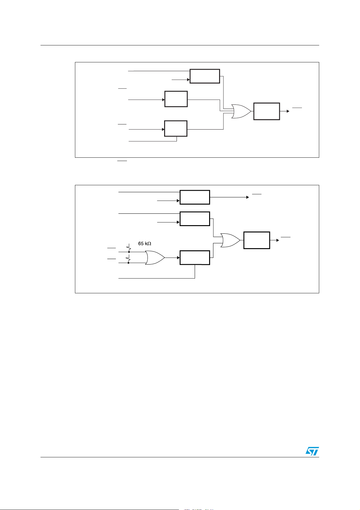
Figure 3. Block diagram - STM6502, STM6503, STM6504
V
CC
SR1
(SRE
STM6504
(1)
only)
V
RST
Logic
COMPARE
t
REC
generator
RST
SR0
SRC (STM6502)
TSR (STM6503,
STM6504)
1. STM6504 only: SR0 and SRE are working independently. SRE is edge-triggered and has a special
debounce time (t
DEBOUNCE
= 240 ms min.) at the falling edge after a valid reset period.
Logic
Figure 4. Block diagram - STM6505
6
"!4
6
##
32
32
32#
6
##
6
"!44(
6
234
#/-
#/-
,OGIC
0!2%
0!2%
",$
T
GENE
2%#
RATOR
234
AM00352a
!-B
8/29 Doc ID 16101 Rev 6
STM6502, STM6503, STM6504, STM6505 Description
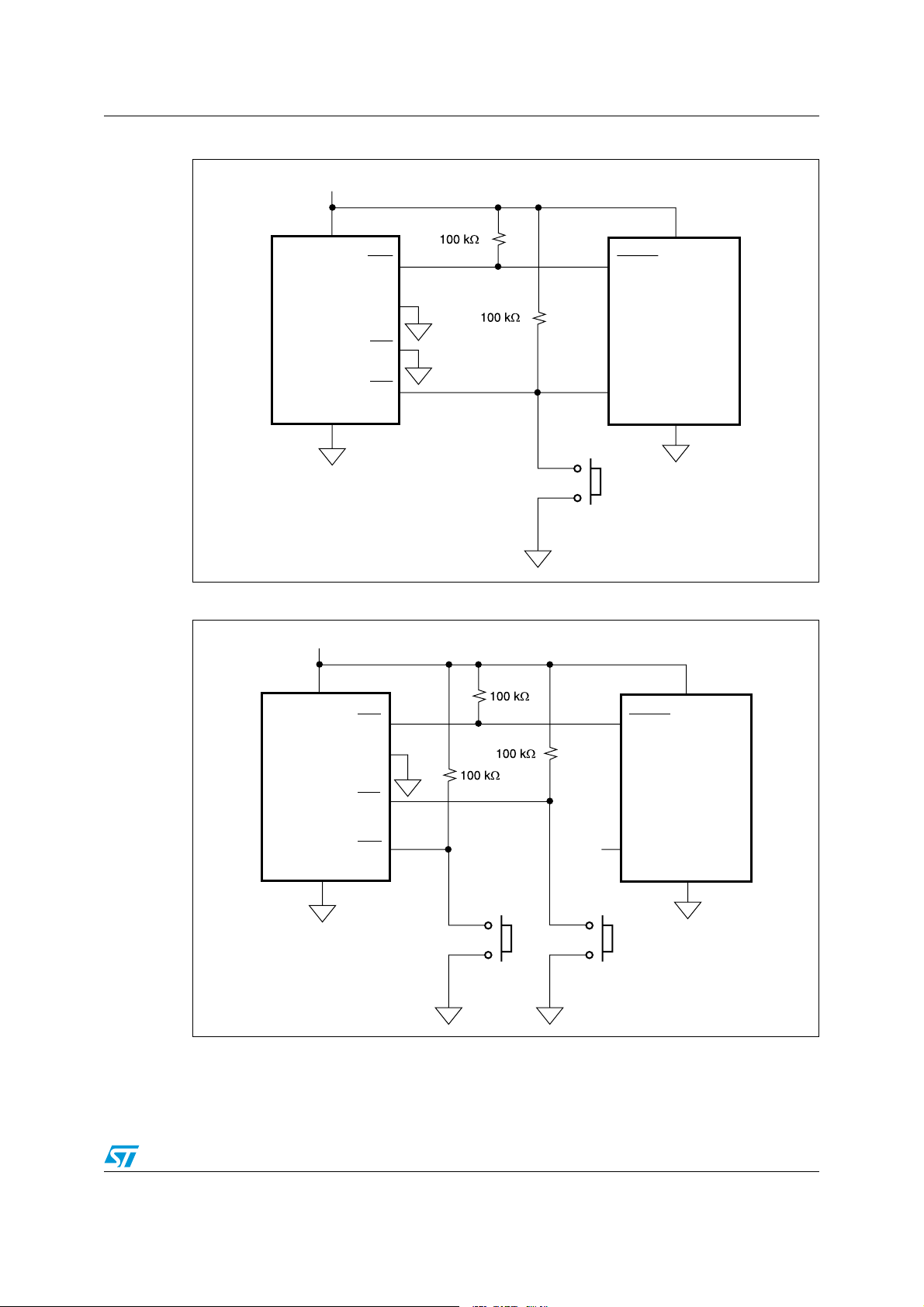
Figure 5. Single-button Smart Reset typical hookup
6
##
6
##
234
432
34-
32
6
32
33
Figure 6. Dual-button Smart Reset typical hookup
6
##
2%3%4
).4
.-)
053(
37)4#(
6
##
-#5
6
33
"544/.
!-B
6
##
34-
6
33
234
432
32
32
053("544/.
37)4#(
053(
37)4#(
2%3%4
).4
.-)
"544/.
6
##
-#5
6
33
!-6
Doc ID 16101 Rev 6 9/29
 Loading...