


查询STM1403供应商
FEATURES*
STM1403
3V FIPS-140
Security Supervisor with Battery Switchover
DATA BRIEFING
■ STM1403 SUPPORTS FIPS-140 SECURITY
LEVEL 3+
– 4 High-Impedance Physical Tamper
Inputs
– Over/Under Operating Voltage Detector
– Security Alarm (SAL
) on Tamper
Detection
■ SUPERVISORY FUNCTIONS
– Automatic Battery Switchover
–RST
– Manual (Push-button) Reset Input (MR
– Power-fail Comparator (PFI/PFO
■ Vccsw (V
– Low When Switched to V
– High When Switched to V
Output (Open Drain)
SWITCH OUTPUT)
CC
CC
(BATT ON
BAT
)
)
Indicator)
■ BATTERY LOW VOLTAGE DETECTOR
(POWER-UP)
■ OPTIONAL V
(1.2 37V)
REF
(Available for STM1403A only)
■ LOW BATTERY SUPPLY CURRENT (2.8µA,
typ)
■ SECURE LOW PROFILE 16-PIN, 3x3mm,
QFN PACKAGE
Figure 1. Package
QFN16, 3mm x 3mm (Q)
Table 1. Device Options
V
V
REF
(1.237V)
Option
is internally switched to battery.
OUT
STM704
Functions
STM1403A ✔✔✔ ✔ON
STM1403B ✔✔✔ Note 3 High-Z High
STM1403C ✔✔✔ Note 3 Ground High
Note: 1. SAL, RST, PFO, and BLD are Open Drain.
2. N ormal Mo de : Lo w when V
3. Pin 9 is the V
pin for STM1403A. It is the V
REF
(1)
Physical
Tamper
Inputs
is internally switched to VCC and High when V
OUT
Over/Under
Voltage
Alarms
pin for STM1 403B/C.
TPU
Over/Under
Temperature
Alarms
Status,
OUT
During
Alarm
Vccsw
During Alarm
Normal Mode
* Contact local ST sales office for the full datasheet.
October 2005
For further information contact your local ST sales office.
Status,
(2)
Rev 4.0
1/9

STM1403
SUMMARY DESCRIPTION
The STM1403 family of security supervisors are a
low power family of intrusion (tamper) detection
chips targeted at manufacturers of POS termi nals
and other systems, to enable them to meet phys-
ical and/or environmental intrusion monitoring
requirements as mandated by vario us standards,
such as Federal Information Processing Standards (FIPS) Pub 140 entitled “Security Requirements for Cryptographic Modules,” published by
the National Institute of Standards and Techn ology, U.S. Department of Commerce), EMVCo, ISO,
ZKA, and VISA PED. STM1403 supports target
levels 3 and lower
The STM1403 includes Automatic Battery
Switchover, RST
(Push-button) Reset Input (MR
parator (PFI/PFO
Output (Open Drain), Manual
), Power-fail Com-
), Physical and/or Environmental
Tamper Detect/Security Alarm, and Battery Low
Voltage Detect features.
The STM1403A also offers a V
(1.237V) as an
REF
option on pin 9. On the STM1403B/C, this pin is
(internally switched VCC or V
V
TPU
BAT
).
Figure 2. Logic Diagram
V
REF
(3)
or
V
BLD
(2)
V
CCSW
MR
PFI
TP1 (NH)
TP
(NL)
Note: 1. V
only for STM1403A; V
REF
2. Normal Mod e: Low when V
and High when V
V
CC
, RST , PFO, and BLD are Open Drain.
3. SAL
V
TPU
STM1403
TP
2
(NH)
(1)
3
OUT
V
BAT
CC
V
OUT
(3)
RST
(3)
PFO
(3)
SAL
V
TP
SS
4
(NL)
for STM1403B/C.
TPU
is internally switched to
OUT
is internally switched to battery.
AI09682
V
Pin Modes
OUT
The STM1403 is available in three versions, corresponding to three modes of the V
Voltage Out), when the SAL
(Sec ur it y Al arm ) i s a s-
pin (Supply
OUT
serted (active-low) upon tamper detection:
STM1403A. V
when SAL
is driven low (activated).
STM1403B. V
stays ON (at VCC or V
OUT
is set to High-Z when SAL is
OUT
BAT
driven low (activated).
STM1403C. V
is activated (may be used when V
directly to the V
is driven to Ground when SA L
OUT
pin of the external SRAM that
CC
is connected
OUT
holds the cryptographic codes).
All variants (see Table 1., Device Options) are pin-
compatible and available in a security-friendly, low
profile, 16-pin QFN package.
Table 2. Signal Names
(1)
Vccsw
MR
PFI Power-fail Input
- TP
TP
1
4
V
OUT
(2)
RST
(2)
PFO
(2)
SAL
(2)
BLD
(3)
V
REF
(3)
V
TPU
V
BA T
V
CC
V
SS
Note: See PIN DESCRIPTIONS, page 9 of the f ull datasheet fo r
details.
1. Normal Mod e: Low when V
V
and High when V
CC
, RST , PFO, and BLD are Open Drain.
2. SAL
only for STM1403A; V
3. V
REF
VCC Switch Output
Manual (Push-button) Reset Input
Independent Physical Tamper
Detect Pins 1 through 4
Supply Voltage Output
Active-low Reset Output
Power-fail Output
Security Alarm Output
Battery Low Voltage Detect
1.237V Reference Voltage
Tamper Pull-up
(V
CC
or V
BAT
)
Back-up Supply Voltage
Supply Voltage
Ground
is internally switched to
OUT
is internally switched to battery.
OUT
for STM1403B/C.
TPU
)
2/9
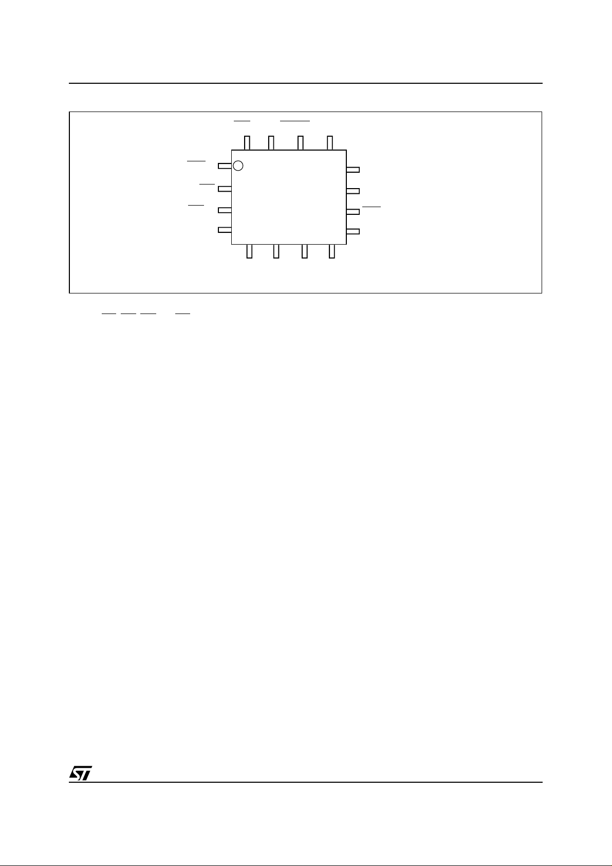
Figure 3. QFN16 Connections
STM1403
(2)
BLD
RST
SAL
MR
V
(2)
(2)
SS
16
1
2
3
4
5
TP
(NH)
Note: See PIN DESCRIPTIONS, page9 of the full datasheet for det ai l s.
1. N ormal Mode: Low wh en V
, RST , PFO, and BLD are Open Drain.
2. SAL
only for STM1403A; V
3. V
REF
is internally switche d to VCC and High when V
OUT
for STM1403B/C.
TPU
V
PFI
CCSW
15
14
76
TP
TP
1
2
(NH)
(NL)
(1)
V
CC
13
V
12
11
10
8
TP
3
4
(NL)
OUT
V
BAT
(2)
PFO
V
9
or
REF
is internally switched to battery.
OUT
V
TPU
AI09683
(3)
3/9

STM1403
Figure 4. Block Diagram
V
CC
(1,2)
BAT54J
(1)
V
BAT
V
OUT
V
SO
COMPARE
V
CCSW
INT
V
V
V
RST
PFI
DET
V
V
HV
LV
V
MR
PFI
TP1 (NH)
TP2 (NL)
TP3 (NH)
TP4 (NL)
Note: 1. BAT54J (from STMicroelectronics) recommended.
2. Required for battery -reverse charging protection.
3. Open Drain
only for STM1403; V
4. V
REF
for STM1403B/C.
TPU
COMPARE
COMPARE
COMPARE @
POWER-UP
1.237V V
REF
Generator
COMPARE
COMPARE
t
rec
Generator
RST
PFO
BLD
V
V
SAL
AI09684
TPU
REF
(3)
(3)
(3)
(4)
(4)
(3)
4/9

TAMPE R DE TECTI O N
STM1403
Physical
There are four (4) high-impedance physical
tamper detect input pins, 2 normall y set to High
(NH) and 2 normally set to Low (NL). Each input is
designed with a glitch immunity. These inputs can
be connected externally to several types of actuator devices (e.g., switches, wire mesh). A tamper
on any one of the four inputs that causes its state
to change will trigger the security alarm (SAL
) and
drive it to active-low. Once the tamper condition no
longer exists, the SAL
will return to its normal High
state.
TP
and TP3 are set Normally to High (NH). They
1
are connected externally through a c losed switch
or a high-impedance resistor to V
of STM1403A) or V
(in the case of STM1403B/
TPU
(in the case
OUT
C), A tam per con dition will be detec ted wh en the
input pin is pulled low. If not used, tie the pin to
or V
V
OUT
and TP4 are set Normally to Low (NL). They
TP
2
TPU
.
are connected externally through a high-impedance resistor or a closed switch to V
. A tamper
SS
condition will be detected when the input pin is
pulled high. If not used, tie the pin to V
SS
.
Supply Voltage
The internally switched supply voltage, V
ther V
itored. If V
point, V
input or V
CC
should exceed th e over vo ltage trip
INT
(set at 4.2V, typical), or should go below
HV
the under voltage trip point, V
cal). SAL
will be driven active-low. Once the
input) is continuously mon-
BAT
(set at 2.0v, typi-
LV
tamper condition no longer exists, the SAL
(ei-
INT
pin will
return to its normal High state.
When no tamper condition exists, SAL
is normally
High.
When a tamper is detected, the SAL
(driven low), independent of the part type. V
is activated
OUT
can be driven to one of three states, depending on
which variant of STM1403 is being used (see De-
vice Options, page 1):
■ ON;
■ High-Z; or
■ Ground (V
SS
).
Note: The STM1403 must be initially powered
above V
alarms. For example, if the battery is on while V
= 0V, no alarm condition can be detected until V
rises above V
to enable the tamper detection
RST
RST
(and t
expires). From this
rec
CC
CC
point on, alarms can be detected either on battery
or V
. This is done to avoid false alarms when
CC
the device goes from no power to its operational
state.
5/9
STM1403
PART NUMBERING
Table 3. Ordering Information Scheme (see Figure 5., page 7 for Marki ng Info rm atio n)
Example: STM1403 A T M – Q 6 F
Device Type
STM1403: Physical, Voltage Tamper Detect
Status (SAL = Active-Low)
V
OUT
A: V
B: V
C: V
Reset Threshold Voltage
= ON; Vccsw = Normal Mode
OUT
= High-Z; Vccsw = High
OUT
= Ground; Vccsw = High
OUT
T: V
S: V
R: V
= 3.00V to 3.15V
RST
= 2.85V to 3.00V
RST
= 2.55V to 2.70V
RST
Battery Low Voltage Detect Threshold (V
M: V
N: V
O: V
= 2.3V (Typ)
DET
= 2.5V (Typ)
DET
= 3.2V (Typ)
DET
Package
Q = QFN16 (3mm x 3mm)
Temperature Range
6 = –40 to 85°C
Shipping Method
F = ECOPACK Package, Tape & Reel
DET
)
For other options, or for more information on any aspect of this device, please contact the ST Sales Office
nearest you.
6/9

Figure 5. Topside Marking Information
Note: 1. Options codes:
X = A, B, o r C (for V
X = T, S, or R (for Reset Threshold)
X = M, N, or O (for Battery Low Vol tage Detect Th reshold)
2. Traceability Codes
Y = Year
WW = Work We ek
OUT
)
XXX
YWW
STM1403
03
(1)
(2)
AI11878
7/9

STM1403
REVISION HISTORY
Table 4. Document Revision History
Date Revision Description
11-October-04 1.0 First Edition
26-Nov-04 1.1
22-Dec-04 1.2 Update characteristics (Figure 5; Table 6, 7, 3)
03-Feb-05 1.3 Update characteristics (Figure 5; Table 6, 7)
25-Feb-05 1.4 Update temperature trip limits (Table 3)
06-May-05 2.0 v2.0 of DB corresponds to v1.5 of DS
05-Aug-05 3.0 v3.0 of DB corresponds to v2.0 of DS
13-Oct-05 4.0 v4.0 of DB corresponds to v3.0 of DS; addition of datasheet availability
Corrected footprint dimensions; update characteristics (Figure 2, 3, 4, 5, 6, 7, 8, 9, 27,
28, 31; Table 1, 2, 3, 6, 7)
8/9

STM1403
Information furnished is believed to be accurate and reliable. However, STMicroelectronics a ssumes no responsibility fo r the c onsequences
of use of such information nor for any infringement of patents or other rights of third parties which may result from its use. No license is granted
by implication or otherwise under any patent or patent rights of STMicroelectronics. Specifications mentioned in this publication are subject
to change without notice. This publication supersedes and replaces all information previously supplied. STMicroelectronics products are not
authori zed for use as crit i cal compon ents in life support devic es or systems without express written approval of STMicroel ectronics.
The ST logo is a registered trademark of STM i croelectr onics.
All other nam es are the pro perty of their respectiv e owners
© 2005 STMi croelectro ni cs - All righ ts reserved
Australi a - Belgium - B razil - Canada - China - Czech Republi c - Finland - France - Germ any - Hong Ko ng - India - Israel - Italy - Japan -
Malaysia - M al ta - Morocco - Singapore - Spain - Swe d en - Switze rl and - United Kingdom - United States of America
STMicroelectron ics group of com panies
www.st.com
9/9
 Loading...