

Features
■ Meets or exceeds the requirements of ANSI
TIA/EIA-644 standard
■ Low voltage differential signaling with typical
output voltage of 350 mV and a 100 Ω load
■ Typical output voltage rise and fall times of
750 ps (400 Mbps)
■ Typical propagation delay times of 1.7 ns
■ Operates from a single 3.3 V supply
■ Power dissipation 25 mW typical per driver at
200 MHz
■ Driver at high impedance when disabled or with
V
= 0 V
CC
■ Pin compatible with the AM26LS31,
SN65LVDS31
■ Low voltage TTL (LVTTL) logic input levels
STLVDS31B
High speed differential line drivers
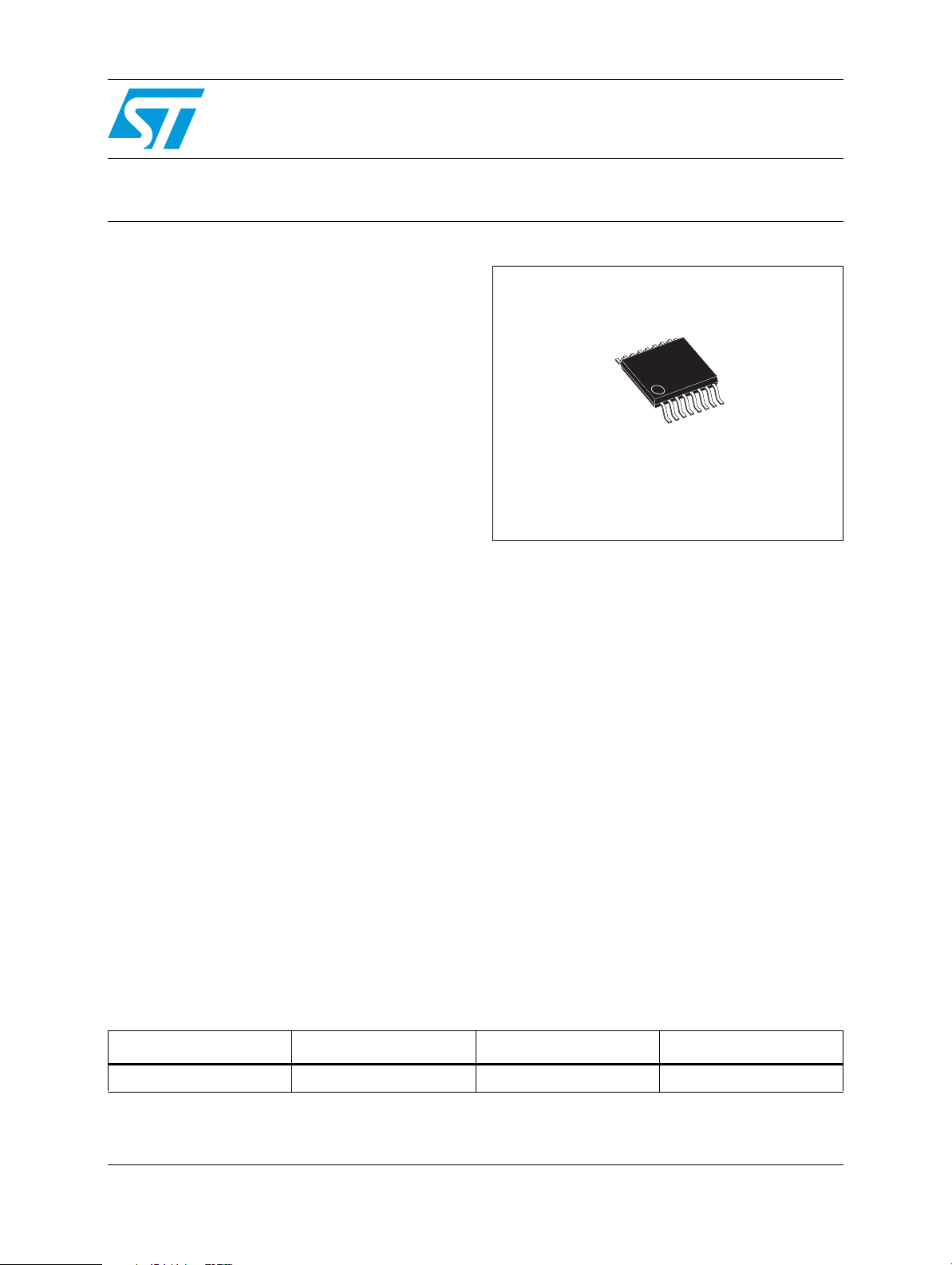
TSSOP16
transmission media may be printed circuit board
traces, backplanes or cables. The ultimate rate
and distance of data transfer is dependent upon
the attenuation characteristics of the media and
noise coupling to the environment.
Description
The STLVDS31B is a quad differential line drivers
that implements the electrical characteristics of
low voltage differential signaling (LVDS). This
signaling technique lowers the output voltage
levels of 5 V differential standard levels (such as
TIA/EIA-422B) to reduce the power, increase the
switching speeds and allows operations with a
3.3 V supply rail. Any of the four current mode
drivers will deliver a minimum differential output
voltage magnitude of 247 mV into a 100 Ω load
when enabled.
The intended application of this device and
signalling technique is for point-to-point baseband
data transmission over controlled
impedancemedia approximately 100 Ω. The
Table 1. Device summary
Order code Temperature range Package Packaging
STLVDS31BTR - 40 to 85 °C TSSOP16 (tape and reel) 2500 parts per reel
The STLVDS31B is characterized for operation
from - 55 °C to 125 °C.
July 2009 Doc ID 8338 Rev 6 1/15
www.st.com
15

Contents STLVDS31B
Contents
1 Pin configuration . . . . . . . . . . . . . . . . . . . . . . . . . . . . . . . . . . . . . . . . . . . 3
2 Maximum ratings . . . . . . . . . . . . . . . . . . . . . . . . . . . . . . . . . . . . . . . . . . . . 5
3 Electrical characteristics . . . . . . . . . . . . . . . . . . . . . . . . . . . . . . . . . . . . . 6
4 Typical characteristics . . . . . . . . . . . . . . . . . . . . . . . . . . . . . . . . . . . . . . . 8
5 Typical performance characteristics . . . . . . . . . . . . . . . . . . . . . . . . . . . 10
6 Package mechanical data . . . . . . . . . . . . . . . . . . . . . . . . . . . . . . . . . . . . 11
7 Revision history . . . . . . . . . . . . . . . . . . . . . . . . . . . . . . . . . . . . . . . . . . . 14
2/15 Doc ID 8338 Rev 6
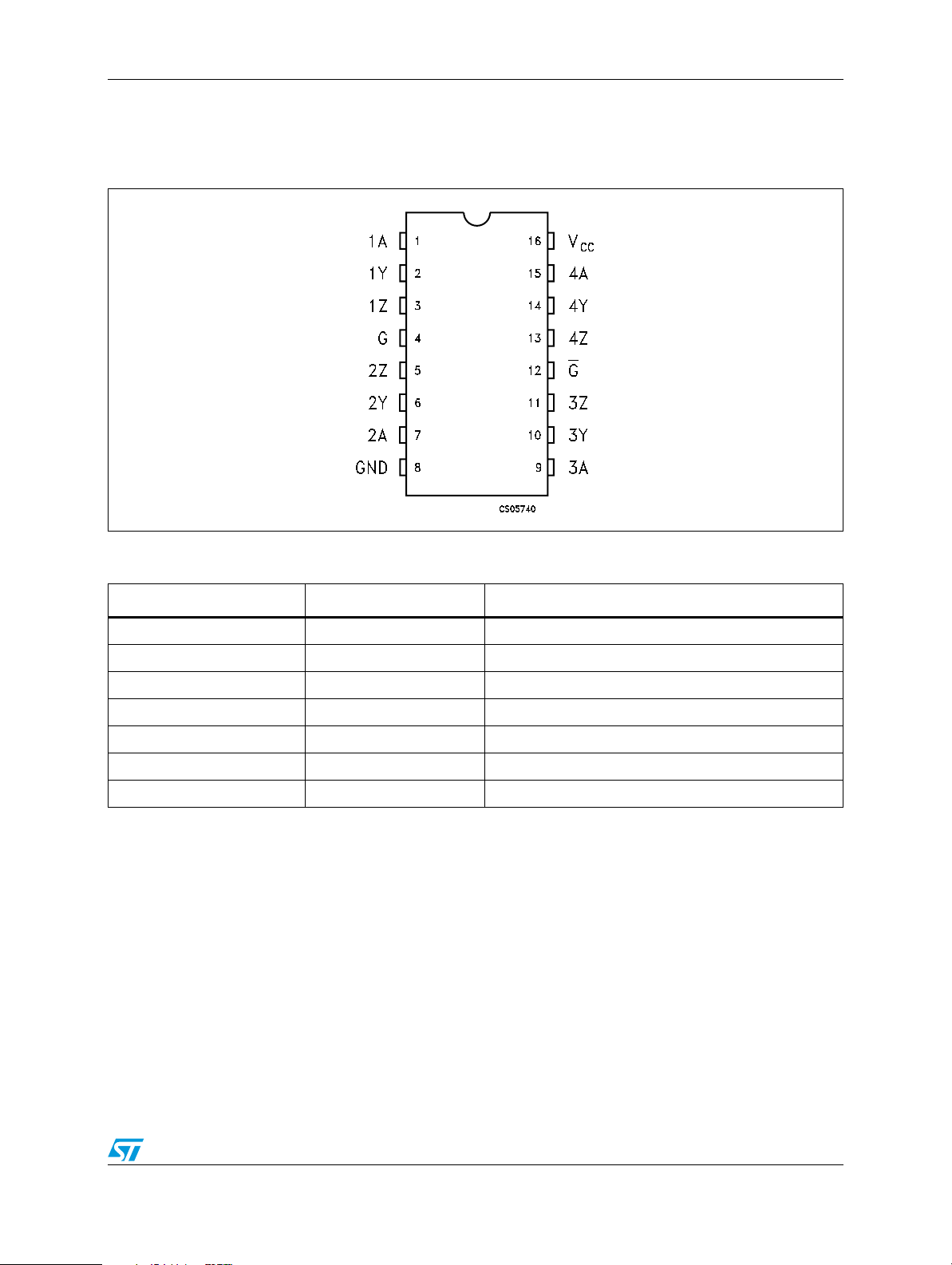
STLVDS31B Pin configuration
1 Pin configuration
Figure 1. Pin connections and functional diagram
Table 2. Pin description
Pin n° Symbol Name and function
1, 7, 9, 15 1A to 4A Driver inputs
2, 6, 10, 14 1Y to 4Y Driver outputs
3, 5, 11, 13 1Z to 4Z Driver outputs
4 G Enable
12 G Enable
8 GND Ground
16 V
CC
Supply voltage
Doc ID 8338 Rev 6 3/15

Pin configuration STLVDS31B
Figure 2. Logic diagram and logic symbol
Table 3. Truth table for receiver
- 100 mV < V
Table 4. Truth table
Input Enables Outputs
AGG
HHXHL
LHXLH
HXLHL
LXLLH
XLHZZ
OPEN H X L H
OPEN X L L H
VID = VA - V
V
≥ 100 mV H
ID
≤ −100 mV L
V
ID
B
< 100 mV ?
ID
OPEN H
YZ
R
L = Low level, H = High Level, X = Don’t care, Z = High Impedance
4/15 Doc ID 8338 Rev 6

STLVDS31B Maximum ratings
2 Maximum ratings
Table 5. Absolute maximum ratings
Symbol Parameter Value Unit
(1)
-0.5 to 4.6 V
T
V
STG
V
CC
I
Supply voltage
DC input voltage -0.5 to (VCC + 0.5) V
Storage temperature range -65 to +150 °C
1. All voltages except differential I/O bus voltage, are with respect to the network ground terminal.
Note: Absolute maximum ratings are those values beyond which damage to the device may occur.
Functional operation under these condition is not implied.
Table 6. Recommended operating conditions
Symbol Parameter Min. Typ. Max. Unit
V
CC
V
IH
V
ILI
T
A
Supply voltage 3.0 3.3 3.6 V
HIGH level input voltage 2.0 V
LOW level input voltage 0.8 V
Operating temperature range -40 85 °C
Doc ID 8338 Rev 6 5/15

Electrical characteristics STLVDS31B
3 Electrical characteristics
Over recommended operating conditions unless otherwise noted. All typical values are at
T
= 25 °C, and VCC = 3.3 V.
A
Table 7. Electrical characteristics
Symbol Parameter Test condition Min. Typ. Max. Unit
ΔV
ΔV
V
V
V
OD
OD
OC(SS)
OC(SS)
OC(PP)
I
CC
I
IH
I
IL
I
SC
I
OZ
I
CS
I
OFF
C
IN
Differential output voltage
Change in differential output
voltage between logic state
R
= 100Ω, Figure 2
L
247 350 454 mV
-50 50 mV
Change in steady-state
common mode output voltage
Figure 3 1.125 1.2 1.375 V
between logic state
Steady-state common mode
output voltage
Peak to peak common mode
output voltage
Supply current
Figure 3 -50 50 mV
80 150 mV
= 0.8V or 2V, Enabled, No Load 11.5 20 mA
V
IN
V
= 0.8V or 2V, Enabled, RL = 100Ω 25 35 mA
IN
= 0 or VCC, Disabled 0.3 1 mA
V
IN
High level input current VIH = 2V 4 20 µA
Low level input current VIL = 0.8V 0.6 10 µA
Short circuit output current
or V
O(Y)
= 0 ± 12 mA
V
OD
= 0V 6.1 - 24 mA
O(Z)
V
High impedance output current VO = 0 or 2.4V ± 1µA
Cold spare leakage current VI = 3.6V, VDD = 0V ± 20 µA
Power OFF output current VCC = 0, VO = 2.4V ± 1µA
Input capacitance 3 pF
6/15 Doc ID 8338 Rev 6

STLVDS31B Electrical characteristics
Over recommended operating conditions unless otherwise noted. All typical values are at
T
= 25 °C, and VCC = 3.3 V.
A
Table 8. Switching characteristics
Symbol Parameter Test condition Min. Typ. Max. Unit
(1)
t
PLH
t
PHL
t
sk(P)
t
sk(O)
t
PZH
t
PZL
t
PHZ
t
PLZ
Propagation delay time, low to high
output
Propagation delay time, high to low
output
Differential output signal rise time 0.4 0.5 0.6 ns
t
r
t
Differential output signal fall time 0.4 0.5 0.6 ns
f
Pulse skew (|t
Channel to channel output skew
THL
= t
|) 0.3 0.6 ns
TLH
(2)
Propagation delay time, high
impedance to high level output
Propagation delay time, high
impedance to low level output
Propagation delay time, high level
to high impedance output
Propagation delay time, low level
to high impedance output
1. RS-232 IN to TTL-CMOS OUT (from 50 % to 50 %).
2. t
is the maximum delay time difference between drivers on the same device.
sk(O)
R
= 100Ω, CL = 10pF
L
Figure 2
Figure 4
0.5 1.4 2 ns
11.72.5ns
00.3ns
5.4 15 ns
2.5 15 ns
8.1 15 ns
7.3 15 ns
Doc ID 8338 Rev 6 7/15
Typical characteristics STLVDS31B
4 Typical characteristics
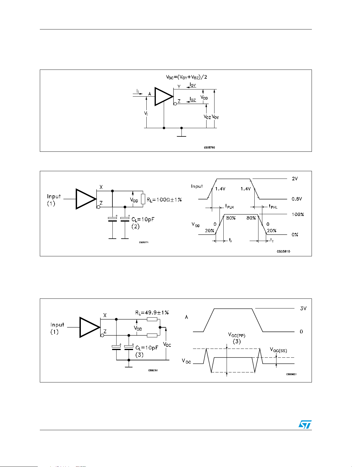
Figure 3. Voltage and current definitions
Figure 4. Test circuit, timing and voltage definitions for differential output signal
1. All input pulse are supplied by a generator having the following characteristics: tr or tf ≤ 1 ns, pulse
repetition rate (PRR) = 50 Mpps, pulse width = 10 ± 0.2 ns.
includes instrumentation and fixture capacitance within 6 mm. of the D.U.T.
2. C
L
Figure 5. Test circuit and definitions for the driver common mode output voltage
1. All input pulse are supplied by a generator having the following characteristics: tr or tf ≤ 1 ns, pulse
repetition rate (PRR) = 50 Mpps, pulse width = 10 ± 0.2 ns.
includes instrumentation and fixture capacitance within 6mm of the D.U.T
2. C
L
3. The measurement of V
is made on test equipment with a -3 dB bandwidth of at least 300 MHz.
OC(PP)
8/15 Doc ID 8338 Rev 6
STLVDS31B Typical characteristics
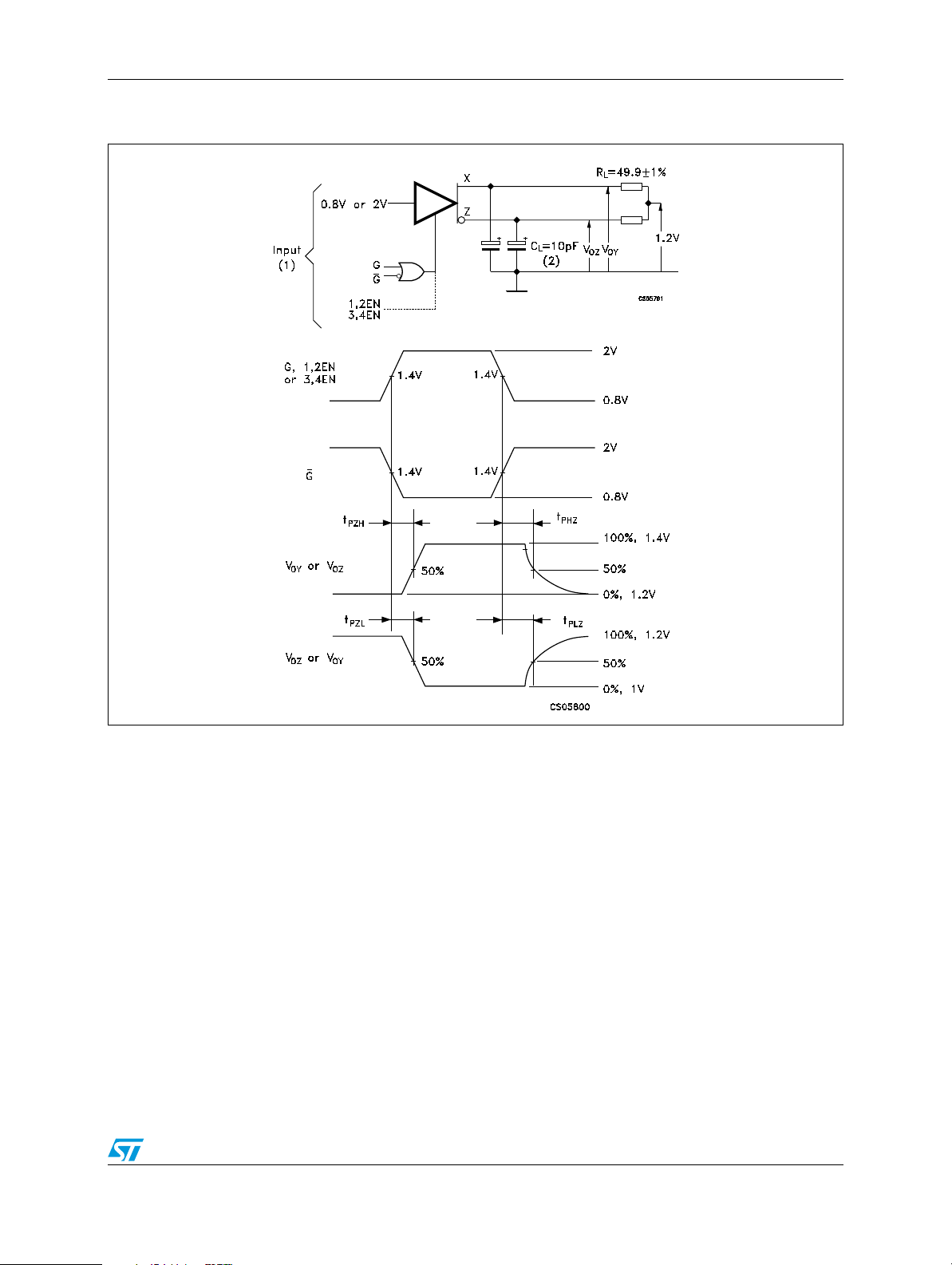
Figure 6. Enable and disable time test circuit and waveform
1. All input pulse are supplied by a generator having the following characteristics: tr or tf ≤ 1 ns, pulse
repetition rate (PRR) = 0.5 Mpps, pulse width = 500 ± 10 ms.
includes instrumentation and fixture capacitance within 6 mm. of the D.U.T.
2. C
L
Doc ID 8338 Rev 6 9/15
Typical performance characteristics STLVDS31B
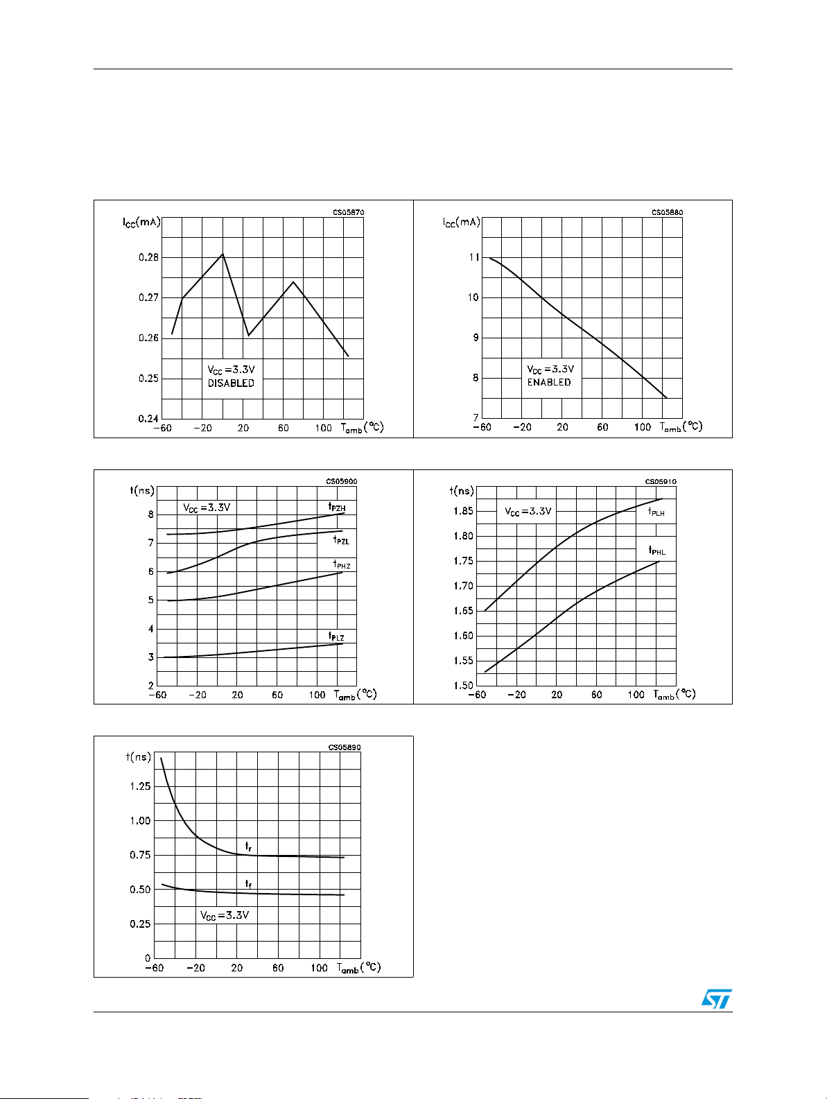
5 Typical performance characteristics
Unless otherwise specified TJ = 25 °C
Figure 7. Supply current vs. temperature Figure 8. Supply current vs. temperature
Figure 9. Propagation delay enable to output Figure 10. Propagation delay time
Figure 11. Differential output signal
10/15 Doc ID 8338 Rev 6

STLVDS31B Package mechanical data
6 Package mechanical data
In order to meet environmental requirements, ST offers these devices in different grades of
ECOPACK
specifications, grade definitions and product status are available at: www.st.com.
ECOPACK
®
packages, depending on their level of environmental compliance. ECOPACK®
®
is an ST trademark.
Doc ID 8338 Rev 6 11/15
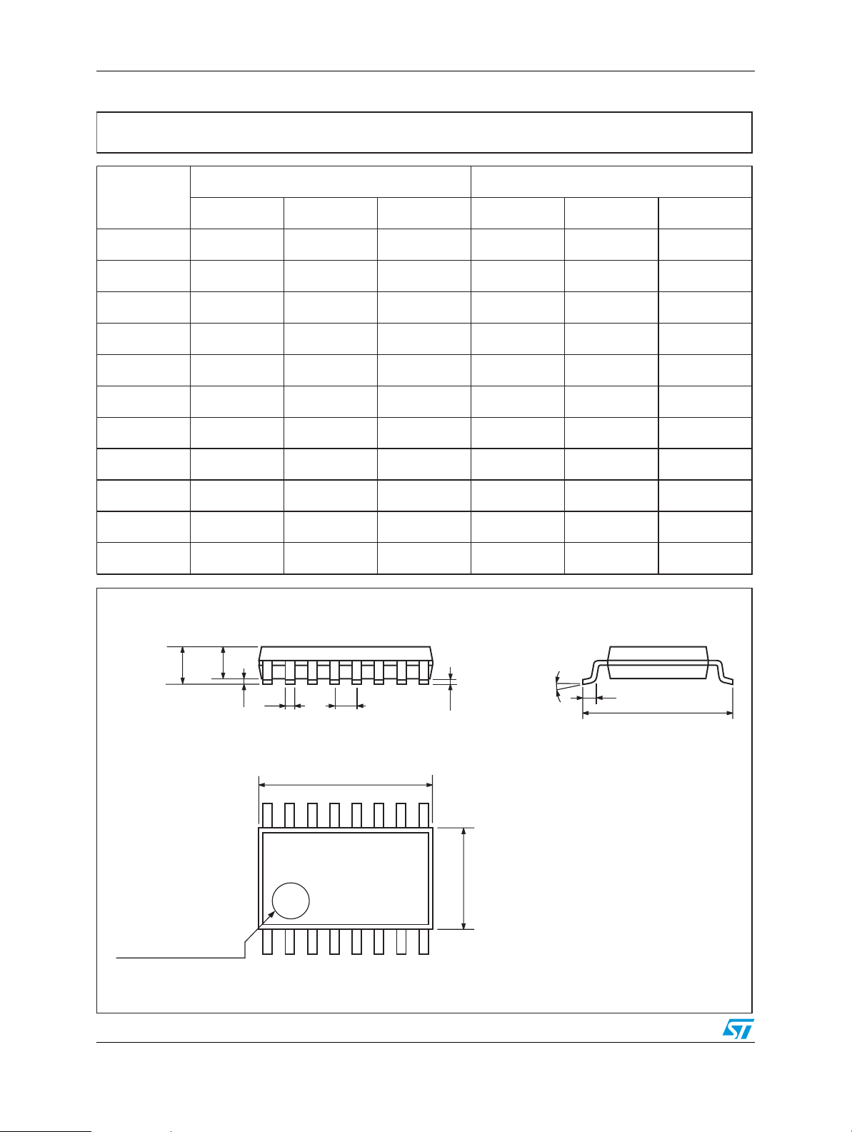
Package mechanical data STLVDS31B
TSSOP16 mechanical data
mm. inch.
Dim.
Min. Typ. Max. Min. Typ. Max.
A 1.2 0.047
A1 0.05 0.15 0.002 0.004 0.006
A2 0.8 1 1.05 0.031 0.039 0.041
b 0.19 0.30 0.007 0.012
c0.09 0.20 0.004 0.0079
D4.9 5 5.1 0.193 0.197 0.201
E 6.2 6.4 6.6 0.244 0.252 0.260
E1 4.3 4.4 4.48 0.169 0.173 0.176
e 0.65 BSC 0.0256 BSC
K0° 8°0° 8°
L 0.45 0.60 0.75 0.018 0.024 0.030
A2
A
A1
b
e
c
K
L
E
D
E1
PIN 1 IDENTIFICATION
1
12/15 Doc ID 8338 Rev 6
0080338D
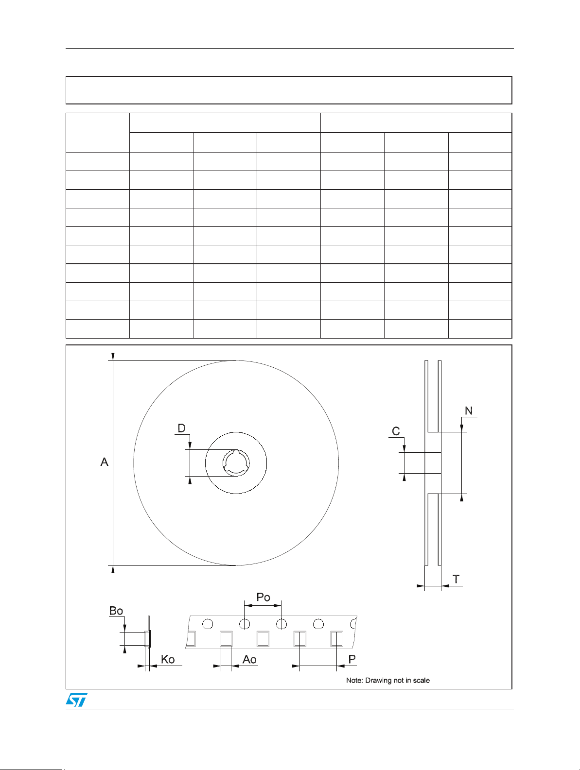
STLVDS31B Package mechanical data
Tape & reel TSSOP16 mechanical data
mm. inch.
Dim.
Min. Typ. Max. Min. Typ. Max.
A 330 12.992
C 12.8 13.2 0.504 0.519
D 20.2 0.795
N60 2.362
T 22.4 0.882
Ao 6.7 6.9 0.264 0.272
Bo 5.3 5.5 0.209 0.217
Ko 1.6 1.8 0.063 0.071
Po 3.9 4.1 0.153 0.161
P7.98.1 0.311 0.319
Doc ID 8338 Rev 6 13/15

Revision history STLVDS31B
7 Revision history
Table 9. Document revision history
Date Revision Changes
28-Mar-2006 5 Order codes updated.
15-Jul-2009 6 Modified: Features on page 1.
14/15 Doc ID 8338 Rev 6

STLVDS31B
Please Read Carefully:
Information in this document is provided solely in connection with ST products. STMicroelectronics NV and its subsidiaries (“ST”) reserve the
right to make changes, corrections, modifications or improvements, to this document, and the products and services described herein at any
time, without notice.
All ST products are sold pursuant to ST’s terms and conditions of sale.
Purchasers are solely responsible for the choice, selection and use of the ST products and services described herein, and ST assumes no
liability whatsoever relating to the choice, selection or use of the ST products and services described herein.
No license, express or implied, by estoppel or otherwise, to any intellectual property rights is granted under this document. If any part of this
document refers to any third party products or services it shall not be deemed a license grant by ST for the use of such third party products
or services, or any intellectual property contained therein or considered as a warranty covering the use in any manner whatsoever of such
third party products or services or any intellectual property contained therein.
UNLESS OTHERWISE SET FORTH IN ST’S TERMS AND CONDITIONS OF SALE ST DISCLAIMS ANY EXPRESS OR IMPLIED
WARRANTY WITH RESPECT TO THE USE AND/OR SALE OF ST PRODUCTS INCLUDING WITHOUT LIMITATION IMPLIED
WARRANTIES OF MERCHANTABILITY, FITNESS FOR A PARTICULAR PURPOSE (AND THEIR EQUIVALENTS UNDER THE LAWS
OF ANY JURISDICTION), OR INFRINGEMENT OF ANY PATENT, COPYRIGHT OR OTHER INTELLECTUAL PROPERTY RIGHT.
UNLESS EXPRESSLY APPROVED IN WRITING BY AN AUTHORIZED ST REPRESENTATIVE, ST PRODUCTS ARE NOT
RECOMMENDED, AUTHORIZED OR WARRANTED FOR USE IN MILITARY, AIR CRAFT, SPACE, LIFE SAVING, OR LIFE SUSTAINING
APPLICATIONS, NOR IN PRODUCTS OR SYSTEMS WHERE FAILURE OR MALFUNCTION MAY RESULT IN PERSONAL INJURY,
DEATH, OR SEVERE PROPERTY OR ENVIRONMENTAL DAMAGE. ST PRODUCTS WHICH ARE NOT SPECIFIED AS "AUTOMOTIVE
GRADE" MAY ONLY BE USED IN AUTOMOTIVE APPLICATIONS AT USER’S OWN RISK.
Resale of ST products with provisions different from the statements and/or technical features set forth in this document shall immediately void
any warranty granted by ST for the ST product or service described herein and shall not create or extend in any manner whatsoever, any
liability of ST.
ST and the ST logo are trademarks or registered trademarks of ST in various countries.
Information in this document supersedes and replaces all information previously supplied.
The ST logo is a registered trademark of STMicroelectronics. All other names are the property of their respective owners.
© 2009 STMicroelectronics - All rights reserved
Australia - Belgium - Brazil - Canada - China - Czech Republic - Finland - France - Germany - Hong Kong - India - Israel - Italy - Japan -
STMicroelectronics group of companies
Malaysia - Malta - Morocco - Philippines - Singapore - Spain - Sweden - Switzerland - United Kingdom - United States of America
www.st.com
Doc ID 8338 Rev 6 15/15
 Loading...