


Features
■ 100ps part-to part skew
■ 50ps bank skew
■ Differential design
■ Meets LVDS spec. for driver outputs and
receiver inputs
■ Reference voltage available output V
Low voltage V
■
■ High signalling rate capability (exceeds
range of 2.375V to 2.625V
CC
BB
622MHz)
■ Support open, short and terminated input fail-
safe (low output state)
■ Programmable drivers power off control
Description
The STLVD111 is a low skew programmable 1 to
10 differential LVDS driver, designed for clock
distribution. The select signal is fanned out to 10
identical differential outputs.
The STLVD111 is provided with a 11 bit shift
register with a serial in and a Control Register.
The purpose is to enable or power off each output
clock channel and to select the clock input. The
STLVD111
Programmable low voltage
1:10 differential LVDS clock driver
TQFP32
STLVD111 is specifically designed, modelled and
produced with low skew as the key goal. Optimal
design and layout serve to minimize gate to gate
skew within a device. The net result is a
dependable guaranteed low skew device.
The STLVD111 can be used for high performance
clock distribution in 2.5V systems with LVDS
levels. Designers can take advantage of the
device’s performance to distribute low skew
clocks across the backplane or the board.
Order codes
Part number
STLVD111BFR -40 to 85 °C TQFP32 (Tape & Reel) 2400 parts per reel
May 2007 Rev. 8 1/19
Temperature
range
Package Packaging
www.st.com
19

STLVD111
Contents
1 Pin configuration . . . . . . . . . . . . . . . . . . . . . . . . . . . . . . . . . . . . . . . . . . . 3
2 Maximum ratings . . . . . . . . . . . . . . . . . . . . . . . . . . . . . . . . . . . . . . . . . . . . 5
3 Electrical characteristics . . . . . . . . . . . . . . . . . . . . . . . . . . . . . . . . . . . . . 6
4 Specification of control register . . . . . . . . . . . . . . . . . . . . . . . . . . . . . . . 8
4.1 Programmed mode (EN=1) . . . . . . . . . . . . . . . . . . . . . . . . . . . . . . . . . . . . 8
4.2 Standard mode (EN=0) . . . . . . . . . . . . . . . . . . . . . . . . . . . . . . . . . . . . . . . 8
5 Diagram . . . . . . . . . . . . . . . . . . . . . . . . . . . . . . . . . . . . . . . . . . . . . . . . . . 10
6 Package mechanical data . . . . . . . . . . . . . . . . . . . . . . . . . . . . . . . . . . . . 15
7 Revision history . . . . . . . . . . . . . . . . . . . . . . . . . . . . . . . . . . . . . . . . . . . 18
2/19

STLVD111 Pin configuration
1 Pin configuration
Figure 1. Pin connections
3/19

Pin configuration STLVD111
Table 1. Pin description
Pin n° Symbol Name and function
1 CK Control register clock
2 SI Control register serial IN/CLK_SEL
3 CLK0 Differential input
4 CLK0 Differential input
5V
BB
6 CLK1 Differential input
7 CLK1 Differential input
8 EN Device enable/program
9 GND Ground
10 Q9 Differential outputs
11 Q9 Differential outputs
12 Q8 Differential outputs
13 Q8 Differential outputs
14 Q7 Differential outputs
Output reference voltage
15 Q7 Differential outputs
16 V
CC
Supply voltage
17 Q6 Differential outputs
18 Q6 Differential outputs
19 Q5 Differential outputs
20 Q5 Differential outputs
21 Q4 Differential outputs
22 Q4 Differential outputs
23 Q3 Differential outputs
24 Q3 Differential outputs
25 GND Ground
26 Q2 Differential outputs
27 Q2 Differential outputs
28 Q1 Differential outputs
29 Q1 Differential outputs
30 Q0 Differential outputs
31 Q0 Differential outputs
32 V
CC
Supply voltage
4/19
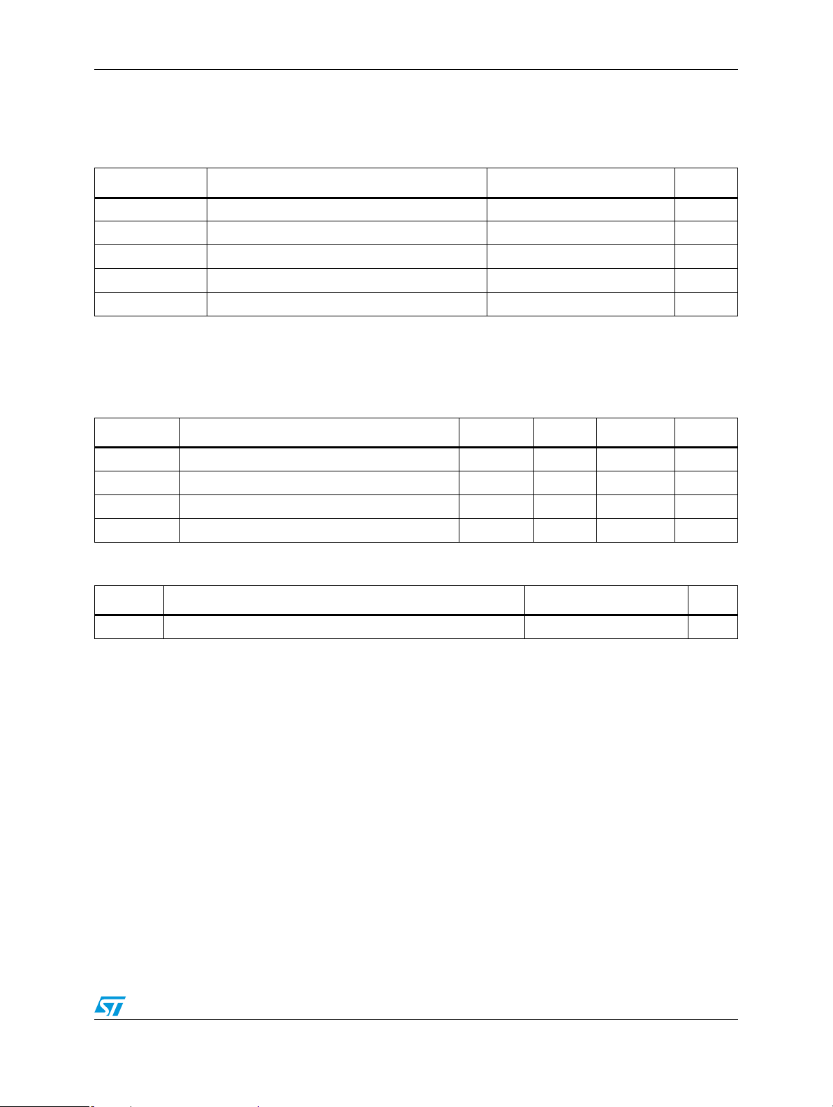
STLVD111 Maximum ratings
2 Maximum ratings
Table 2. Absolute maximum ratings
Symbol Parameter Value Unit
V
V
V
I
OSD
CC
I
O
Supply voltage -0.3 to 2.8 V
Input voltage -0.2 to (VCC+0.2) V
Output voltage -0.2 to (VCC+0.2) V
Driver short circuit current Continuous
ESD Electrostatic discharge (HBM 1.5KΩ, 100pF) >2 KV
Note: Absolute Maximum Ratings are those values beyond which damage to the device may
occur. Functional operation under these condition is not implied.
Table 3. Recommended operating conditions
Symbol Parameter Min. Typ. Max. Unit
V
CC
V
IC
T
A
T
J
Supply voltage 2.375 2.625 V
Receiver common mode input voltage 0.5(VID) 2-0.5(VID)V
Operating free-air temperature range -40 85 °C
Operating junction temperature -40 105 °C
Table 4. Thermal data
Symbol Parameter Value Unit
R
thJC
Thermal resistance junction-case 13 °C/W
5/19
Electrical characteristics STLVD111
3 Electrical characteristics
Table 5. Driver electrical characteristics (T
= -40 to 85 °C, VCC = 2.5V ± 5%, unless otherwise
A
specified Note: 1, 2)
Symbol Parameter Test condition Min. Typ. Max. Unit
V
ΔV
V
ΔV
I
OS
Output differential voltage (Figure 4.)RL = 100 Ω 400 500 600 mV
OD
VOD magnitude change 30 mV
OD
Offset voltage -40 ≤ TA ≤ 85°C 1.05 1.15 1.25 V
OS
VOS magnitude change 30 V
OS
V
= 0V 15 30
Output short circuit current
O
= 0V 7 15
V
OD
mA
Note: 1 All currents into device pins are positive; all currents out of device pins are negative. All
voltages are referenced to device ground unless otherwise specified.
2 All typical values are given for V
= 2.5V and TA = 25°C unless otherwise stated
CC
Table 6. Receiver electrical characteristics (TA = -40 to 85 °C, VCC = 2.5V ± 5%, unless otherwise
specified Note: 1, 2)
Symbol Parameter Test condition Min. Typ. Max. Unit
V
IDH
V
IDL
I
IN
Input threshold high 100 mV
Input threshold low -100 mV
V
= 0V 42 100
Input current
V
I
= 0V
I
CC
210
μA
Note: 1 All currents into device pins are positive; all currents out of device pins are negative. All
voltages are referenced to device ground unless otherwise specified.
2 All typical values are given for V
6/19
= 2.5V and TA = 25°C unless otherwise stated
CC

STLVD111 Electrical characteristics
Table 7. Driver electrical characteristics (T
= -40 to 85 °C, VCC = 2.5V ± 5%, unless otherwise
A
specified Note: 1, 2)
Symbol Parameter Test condition Min. Typ. Max. Unit
V
I
CCD
C
C
V
V
Output reference voltage VCC = 2.5 V 1.15 1.25 1.35 V
BB
Power supply current All driver enabled and loaded 125 160 mA
Input capacitance VI = 0V to V
IN
Output capacitance 5 pF
OUT
Logic input high threshold VCC = 2.5 V 2 V
IH
Logic input low threshold VCC = 2.5 V 0.8 V
IL
Logic input current VCC = 2.5 V, VIN = VCC or GND ±10 µA
I
I
CC
5pF
Note: 1 All currents into device pins are positive; all currents out of device pins are negative. All
voltages are referenced to device ground unless otherwise specified
2 All typical values are given for V
= 2.5V and TA = 25°C unless otherwise stated
CC
Table 8. LVDS timing characteristics (TA = -40 to 85 °C, VCC = 2.5V ± 5%, unless otherwise
specified)
Symbol Parameter Test condition Min. Typ. Max. Unit
R
= 100 Ω, CL = 5 pF,
t
TLH, tTHL
t
PHL, tPLH
f
MAX
t
SKEW
Transition time
Propagation delay time (Figure 7., Figure 8.)22.5ns
Maximum input frequency 700 900 MHz
Bank skew (Figure 3.)50
Pulse skew (Figure 5.)50
L
Figure 7., Figure 8.)
220 300 ps
psPart to part skew (Figure 4.) 100
Table 9. Control register timing characteristics (TA = -40 to 85 °C, VCC = 2.5V ± 5%, unless
otherwise specified)
Symbol Parameter Test condition Min. Typ. Max. Unit
f
MAX
t
rem
t
t
t
W
Maximum frequency of shift register (Figure 9.) 100 150 MHz
Clock to SI setup time (Figure 9.)2ns
s
Clock to SI hold time (Figure 9.)1.5ns
h
Enable to clock removal time (Figure 9.)1.5ns
Minimum clock pulse width (Figure 9.)3 ns
7/19

Specification of control register STLVD111
4 Specification of control register
The STLVD111 is provided with a 11 bit shift register with a Serial In and a Control Register.
The purpose is to enable or power of each output clock channel and to select the clock
input. The STLVD111 provides two working modality:
4.1 Programmed mode (EN=1)
The shift register have a serial input to load the working configuration. Once the
configuration is loaded with 11 clock pulse, another clock pulse load the configuration into
the control register. The first bit on the serial input line enables the outputs Q9 and Q9, the
second bit enables the outputs Q8 and Q8 and so on. The last bit is the clock selection bit.
To restart the configuration of the shift register a reset of the state machine must be done
with a clock pulse on CK and the EN set to Low. The control register shift register can be
configured on time after each reset.
4.2 Standard mode (EN=0)
In Standard Mode the STLVD111 isn’t programmable, all the clock outputs are enabled. The
LVDS clock input is selected from Clock 0 or Clock 1 with the SI pin as shown in the Truth
Table below.
Table 10. Truth table of state machine inputs
EN SI CK Output
L L X All output enabled, Clock 0 selected, control register disabled
L H X All output enabled, Clock 1 selected, control register disabled
H L First stage stores "L", other stages store the data of previous stage
H H First stage stores "H", other stages store the data of previous stage
L X Reset of the state machine, shift register and control register
Table 11. Serial input sequence
BIT#10 BIT#9 BIT#8 BIT#7 BIT#6 BIT#5 BIT#4 BIT#3 BIT#2 BIT#1 BIT#0
CLK_SEL Q0 Q1 Q2 Q3 Q4 Q5 Q6 Q7 Q8 Q9
Table 12. Truth table of the control register
BIT#10 BIT#(0-9) Qn(0-9)
L H Clock 0
H H Clock 1
8/19
X L Qn Output Disabled

STLVD111 Specification of control register
Table 13. Truth table
CK EN SI CLK 0 CLK 0 CLK 1 CLK 1 Q (0-9) Q(0-9)
LLLLHXXLH
LLLHLXXHL
L L L Open Open X X L H
LLHXXLHLH
LLHXXHLHL
L L H X X Open Open L H
All drivers enable
9/19

Diagram STLVD111
5 Diagram
Figure 2. Logic diagram
10/19

STLVD111 Diagram
Figure 3. Bank skew - t
1. BANKSKEW is the magnitude of the time difference between outputs with a single driving input terminal
Figure 4. Part to part skew - t
sk(b)
(1)
sk(PP)
(1)
1. PART TO PART SKEW is the magnitude of the difference in propagation delay times between any specific terminals of two
devices when both devices operate with the same input signals, the same supply voltages, and the same temperature, and
have identical packages and test circuits.
11/19

Diagram STLVD111
Figure 5. Pulse skew - t
1. PULSE SKEW is the magnitude of the time difference between the high to low and low to high propagation delay times at
an output.
sk(P)
(1)
Figure 6. Voltage and current definition
12/19

STLVD111 Diagram
Figure 7. Test circuit and voltage definition for the differential output signal
.
Figure 8. Differential receiver to drive propagation delay and drive transition time waveforms
13/19

Diagram STLVD111
Figure 9. Set-Up, hold and the removal time, maximum frequency, minimum pulse width
waveforms
14/19

STLVD111 Package mechanical data
6 Package mechanical data
In order to meet environmental requirements, ST offers these devices in ECOPACK®
packages. These packages have a Lead-free second level interconnect. The category of
second Level Interconnect is marked on the package and on the inner box label, in
compliance with JEDEC Standard JESD97. The maximum ratings related to soldering
conditions are also marked on the inner box label. ECOPACK is an ST trademark.
ECOPACK specifications are available at: www.st.com.
15/19

Package mechanical data STLVD111
D
TQFP32 MECHANICAL DATA
DIM.
mm. inch
MIN. TYP MAX. MIN. TYP. MAX.
A 1.6 0.063
A1 0.05 0.15 0.002 0.006
A2 1.35 1.40 1.45 0.053 0.055 0.057
B 0.30 0.37 0.45 0.012 0.015 0.018
C 0.09 0.20 0.0035 0.0079
D 9.00 0.354
D1 7.00 0.276
D3 5.60 0.220
e 0.80 0.031
E 9.00 0.354
E1 7.00 0.276
E3 5.60 0.220
L 0.45 0.60 0.75 0.018 0.024 0.030
L1 1.00 0.039
K 0°3.5°7° 0°3.5°7°
D1
A1
1724
25
B
32
1
e
8
TQFP32
16
L1
E
L
K
E3D3E1
9
0.10mm
.004
Seating Plane
B
A
A2
C
0060661/C
16/19

STLVD111 Package mechanical data
Tape & Reel TQFP32 MECHANICAL DATA
mm. inch
DIM.
MIN. TYP MAX. MIN. TYP. MAX.
A 330 12.992
C 12.8 13.2 0.504 0.519
D 20.2 0.795
N 60 2.362
T 22.4 0.882
Ao 9.5 9.7 0.374 0.382
Bo 9.5 9.7 0.374 0.382
Ko 2.1 2.3 0.083 0.091
Po 3.9 4.1 0.153 0.161
P 11.9 12.1 0.468 0.476
17/19

Revision history STLVD111
7 Revision history
Table 14. Revision history
Date Revision Changes
30-May-2007 8 Order codes has been updated and the document has been reformatted.
18/19

STLVD111
Please Read Carefully:
Information in this document is provided solely in connection with ST products. STMicroelectronics NV and its subsidiaries (“ST”) reserve the
right to make changes, corrections, modifications or improvements, to this document, and the products and services described herein at any
time, without notice.
All ST products are sold pursuant to ST’s terms and conditions of sale.
Purchasers are solely responsible for the choice, selection and use of the ST products and services described herein, and ST assumes no
liability whatsoever relating to the choice, selection or use of the ST products and services described herein.
No license, express or implied, by estoppel or otherwise, to any intellectual property rights is granted under this document. If any part of this
document refers to any third party products or services it shall not be deemed a license grant by ST for the use of such third party products
or services, or any intellectual property contained therein or considered as a warranty covering the use in any manner whatsoever of such
third party products or services or any intellectual property contained therein.
UNLESS OTHERWISE SET FORTH IN ST’S TERMS AND CONDITIONS OF SALE ST DISCLAIMS ANY EXPRESS OR IMPLIED
WARRANTY WITH RESPECT TO THE USE AND/OR SALE OF ST PRODUCTS INCLUDING WITHOUT LIMITATION IMPLIED
WARRANTIES OF MERCHANTABILITY, FITNESS FOR A PARTICULAR PURPOSE (AND THEIR EQUIVALENTS UNDER THE LAWS
OF ANY JURISDICTION), OR INFRINGEMENT OF ANY PATENT, COPYRIGHT OR OTHER INTELLECTUAL PROPERTY RIGHT.
UNLESS EXPRESSLY APPROVED IN WRITING BY AN AUTHORIZE REPRESENTATIVE OF ST, ST PRODUCTS ARE NOT DESIGNED,
AUTHORIZED OR WARRANTED FOR USE IN MILITARY, AIR CRAFT, SPACE, LIFE SAVING, OR LIFE SUSTAINING APPLICATIONS,
NOR IN PRODUCTS OR SYSTEMS, WHERE FAILURE OR MALFUNCTION MAY RESULT IN PERSONAL INJURY, DEATH, OR
SEVERE PROPERTY OR ENVIRONMENTAL DAMAGE.
Resale of ST products with provisions different from the statements and/or technical features set forth in this document shall immediately void
any warranty granted by ST for the ST product or service described herein and shall not create or extend in any manner whatsoever, any
liability of ST.
ST and the ST logo are trademarks or registered trademarks of ST in various countries.
Information in this document supersedes and replaces all information previously supplied.
The ST logo is a registered trademark of STMicroelectronics. All other names are the property of their respective owners.
© 2007 STMicroelectronics - All rights reserved
STMicroelectronics group of companies
Australia - Belgium - Brazil - Canada - China - Czech Republic - Finland - France - Germany - Hong Kong - India - Israel - Italy - Japan -
Malaysia - Malta - Morocco - Singapore - Spain - Sweden - Switzerland - United Kingdom - United States of America
www.st.com
19/19
 Loading...