

50 mA, 3 µA supply current low drop linear regulator
Features
■ 2.3 V to 12 V input voltage range
■ 50 mA maximum output current
■ 3 µA quiescent current
■ Available in 1.8 V, 2.5 V, 3.3 V, 5.0 V and
adjustable
■ 200 mV dropout voltage at 25 mA output
current
■ Internal thermal protection
■ Available in SOT323-5L package, and SOT23-
5L package (upon request)
Applications
■ Portable/battery powered equipments
■ Electronic sensors
■ Microcontroller power
■ Real time clock backup power
STLQ50XX
SOT323-5L
Description
The STLQ50 is a BiCMOS linear regulator
specifically designed for operating in environment
with very low power consumption constraints.
Due to the very low quiescent current (3 µA) the
device is suitable for those application that have
very long stand-by time allowing extension of
battery life.
The P-MOS pass element allows also a very good
drop-out figure (200 mV at 25 mA I
at full load) without affecting the consumption
characteristics.
SOT23-5L
(available on request)
and 350 mV
O
Housed in the very small SOT323-5L or SOT235L, it fulfils the space saving requirements in
battery powered equipments.
Table 1. Device summary
Order codes
Part number
SOT323-5L (T&R) SOT23-5L (T&R)
STLQ50XX18 STLQ50C18R STLQ50M18R Fixed VO = 1.8V
STLQ50XX25 STLQ50C25R STLQ50M25R Fixed V
STLQ50XX33 STLQ50C33R STLQ50M33R Fixed V
STLQ50XX50 STLQ50C50R STLQ50M50R Fixed V
STLQ50 STLQ50C-R STLQ50M-R Adjustable
1. Available upon request.
November 2007 Rev. 4 1/18
(1)
Output voltagePackages
= 2.5V
O
= 3.3V
O
= 5.0V
O
www.st.com
18

STLQ50XX
Contents
1 Diagram . . . . . . . . . . . . . . . . . . . . . . . . . . . . . . . . . . . . . . . . . . . . . . . . . . . 3
2 Pin configuration . . . . . . . . . . . . . . . . . . . . . . . . . . . . . . . . . . . . . . . . . . . . 4
3 Maximum ratings . . . . . . . . . . . . . . . . . . . . . . . . . . . . . . . . . . . . . . . . . . . . 5
4 Electrical characteristics . . . . . . . . . . . . . . . . . . . . . . . . . . . . . . . . . . . . . 6
5 Typical application . . . . . . . . . . . . . . . . . . . . . . . . . . . . . . . . . . . . . . . . . . 7
6 Typical characteristics . . . . . . . . . . . . . . . . . . . . . . . . . . . . . . . . . . . . . . . 8
7 Application information . . . . . . . . . . . . . . . . . . . . . . . . . . . . . . . . . . . . . 10
7.1 External components . . . . . . . . . . . . . . . . . . . . . . . . . . . . . . . . . . . . . . . . 10
7.2 Power dissipation . . . . . . . . . . . . . . . . . . . . . . . . . . . . . . . . . . . . . . . . . . . 10
7.3 Protection . . . . . . . . . . . . . . . . . . . . . . . . . . . . . . . . . . . . . . . . . . . . . . . . . 11
8 Package mechanical data . . . . . . . . . . . . . . . . . . . . . . . . . . . . . . . . . . . . 12
9 Revision history . . . . . . . . . . . . . . . . . . . . . . . . . . . . . . . . . . . . . . . . . . . 17
2/18
STLQ50XX Diagram
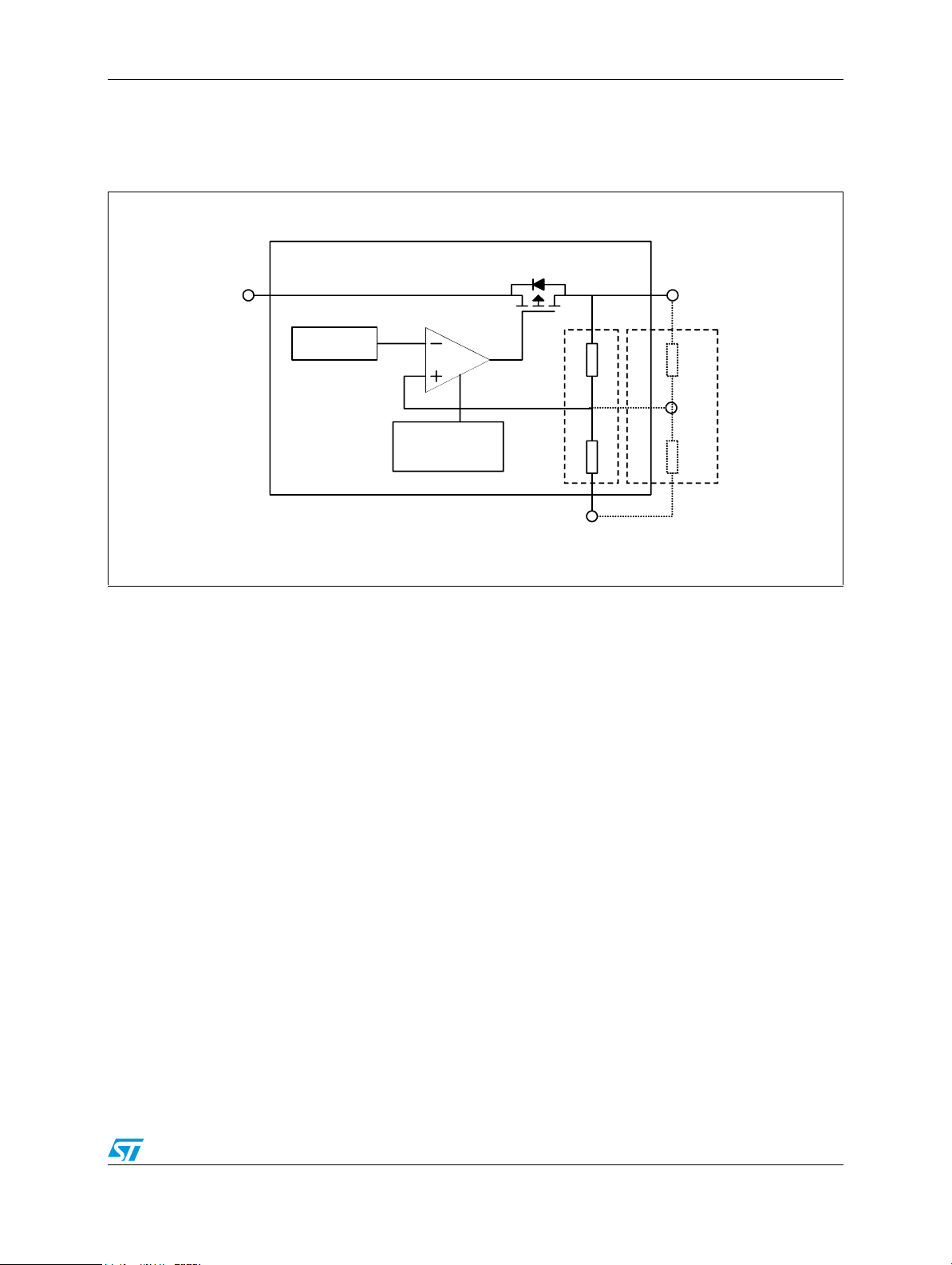
1 Diagram
Figure 1. Block diagram
Vin
V bandgap
1.22V
Vout
Adjustable
Fixed
ADJ
Short circuit &
thermal
protection
GND
3/18
Pin configuration STLQ50XX
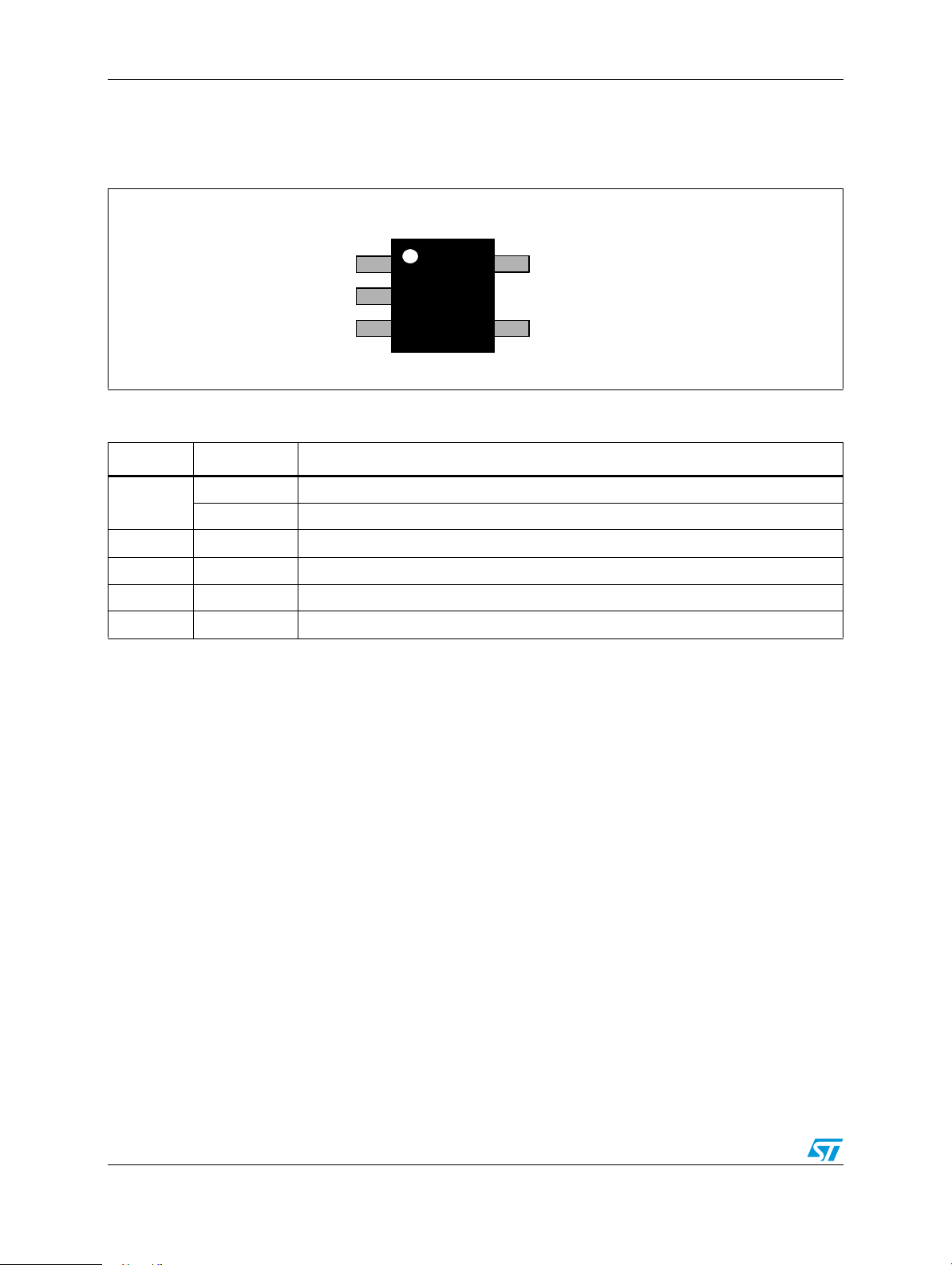
2 Pin configuration
Figure 2. Pin connections (top view)
ADJ
ADJ
STLQ50
GND
GND
N/C
N/C
Table 2. Pin description
Pin n° Symbol Note
1
2 GND Ground
3 N/C Not connected
4 IN Input voltage
5 OUT Output voltage
ADJ STLQ50: output voltage adjust
N/C STLQ50xx: not connected
STLQ50
OUT
OUT
IN
IN
4/18
STLQ50XX Maximum ratings
3 Maximum ratings
Table 3. Absolute maximum ratings
Symbol Parameter Value Unit
V
I
V
FB
DC Input voltage -0.3 to +14 V
FB voltage -0.3 to +7 V
ESD Human body model (all pins) ±2 kV
T
T
J
STG
Junction temperature -40 to 150 °C
Storage temperature range -55 to 150 °C
Note: Absolute maximum ratings are those values beyond which damage to the device may occur.
Functional operation under these conditions is not implied.
Table 4. Thermal data
Symbol Parameter SOT323-5L SOT23-5L Unit
R
thJA
1. This value is referred to a 4-layer PCB, JEDEC standard test board.
Thermal resistance junction-ambient 331.4
(1)
191
(1)
°C/W
5/18
Electrical characteristics STLQ50XX
4 Electrical characteristics
Table 5. Electrical characteristics
(V
= V
I
O(NOM)
are at T
Symbol Parameter Test conditions Min. Typ. Max. Unit
+1 V or VI = 2.5 V if VO + 1.5 V; TA= -40 °C to 125 °C; IO = 1 mA; typical values
= 25 °C, CO = 1 µF unless otherwise specified)
A
V
I
Q
Input voltage range
I
Quiescent current (Measured on
ground pin, fixed version)
=50mA 2.5 12
I
O
=5V 3.5 5.0
V
I
=12V 4.1 6.0
V
I
Output voltage range (STLQ50ADJ) 1.222 11 V
IO=20mA 2.3 12
V
O
Accuracy as percentage of nominal
=25°C
J
V
DROP-MAX
ΔV
ΔV
voltage at T
Max dropout voltage
Load regulation 1mA < IO <50mA 0.15 %/mA
O
Line regulation
O
SVR Supply voltage rejection
eN Output noise voltage
(1)
IO=50mA; 0.4 0.7 V
=1.5V:
V
O
VO+1V < VI <12V;
VO=1.5V:
2.5V < V
V
RIPPLE
<12V;
I
= 0.1V, IO= 20mA
f=120Hz
from 200Hz to
B
W
100KHZ; IO=10mA
-2 +2 %
30 dB
560 µV
Th Thermal protection 160 °C
I
OMAX
1. VI=2.5V when V
2. The maximum power dissipation must not be exceeded, see application information for details.
Maximum output current
≤ 2.1V
O(NOM)
(2)
VO=0V 500 mA
V
µA
0.3 %/V
RMS
6/18
 Loading...