

50 mA, 3 µA supply current low drop linear regulator
Features
■ 2.3 V to 12 V input voltage range
■ 50 mA maximum output current
■ 3 µA quiescent current
■ Available in 1.8 V, 2.5 V, 3.3 V, 5.0 V and
adjustable
■ 200 mV dropout voltage at 25 mA output
current
■ Internal thermal protection
■ Available in SOT323-5L package, and SOT23-
5L package (upon request)
Applications
■ Portable/battery powered equipments
■ Electronic sensors
■ Microcontroller power
■ Real time clock backup power
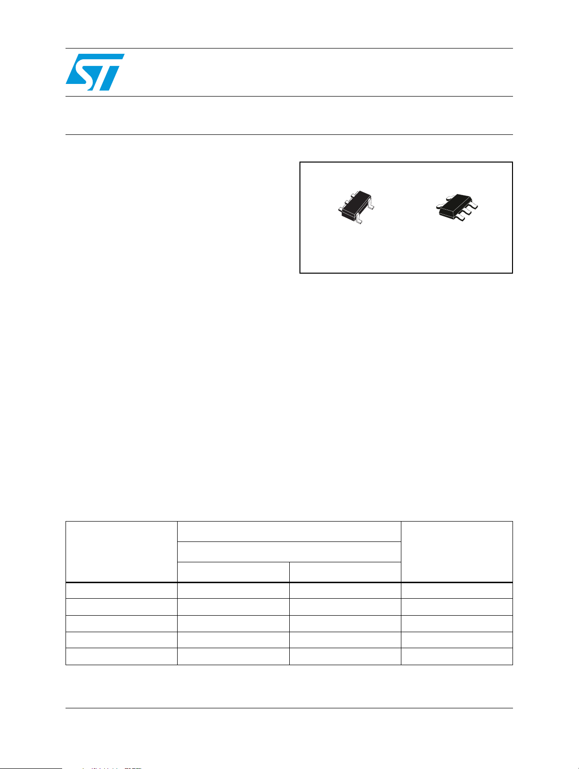
STLQ50XX
SOT323-5L
Description
The STLQ50 is a BiCMOS linear regulator
specifically designed for operating in environment
with very low power consumption constraints.
Due to the very low quiescent current (3 µA) the
device is suitable for those application that have
very long stand-by time allowing extension of
battery life.
The P-MOS pass element allows also a very good
drop-out figure (200 mV at 25 mA I
at full load) without affecting the consumption
characteristics.
SOT23-5L
(available on request)
and 350 mV
O
Housed in the very small SOT323-5L or SOT235L, it fulfils the space saving requirements in
battery powered equipments.
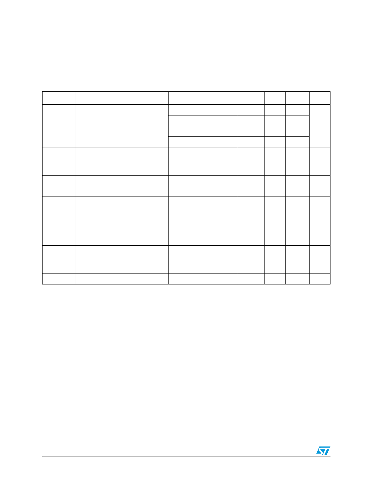
Table 1. Device summary
Order codes
Part number
SOT323-5L (T&R) SOT23-5L (T&R)
STLQ50XX18 STLQ50C18R STLQ50M18R Fixed VO = 1.8V
STLQ50XX25 STLQ50C25R STLQ50M25R Fixed V
STLQ50XX33 STLQ50C33R STLQ50M33R Fixed V
STLQ50XX50 STLQ50C50R STLQ50M50R Fixed V
STLQ50 STLQ50C-R STLQ50M-R Adjustable
1. Available upon request.
November 2007 Rev. 4 1/18
(1)
Output voltagePackages
= 2.5V
O
= 3.3V
O
= 5.0V
O
www.st.com
18

STLQ50XX
Contents
1 Diagram . . . . . . . . . . . . . . . . . . . . . . . . . . . . . . . . . . . . . . . . . . . . . . . . . . . 3
2 Pin configuration . . . . . . . . . . . . . . . . . . . . . . . . . . . . . . . . . . . . . . . . . . . . 4
3 Maximum ratings . . . . . . . . . . . . . . . . . . . . . . . . . . . . . . . . . . . . . . . . . . . . 5
4 Electrical characteristics . . . . . . . . . . . . . . . . . . . . . . . . . . . . . . . . . . . . . 6
5 Typical application . . . . . . . . . . . . . . . . . . . . . . . . . . . . . . . . . . . . . . . . . . 7
6 Typical characteristics . . . . . . . . . . . . . . . . . . . . . . . . . . . . . . . . . . . . . . . 8
7 Application information . . . . . . . . . . . . . . . . . . . . . . . . . . . . . . . . . . . . . 10
7.1 External components . . . . . . . . . . . . . . . . . . . . . . . . . . . . . . . . . . . . . . . . 10
7.2 Power dissipation . . . . . . . . . . . . . . . . . . . . . . . . . . . . . . . . . . . . . . . . . . . 10
7.3 Protection . . . . . . . . . . . . . . . . . . . . . . . . . . . . . . . . . . . . . . . . . . . . . . . . . 11
8 Package mechanical data . . . . . . . . . . . . . . . . . . . . . . . . . . . . . . . . . . . . 12
9 Revision history . . . . . . . . . . . . . . . . . . . . . . . . . . . . . . . . . . . . . . . . . . . 17
2/18
STLQ50XX Diagram
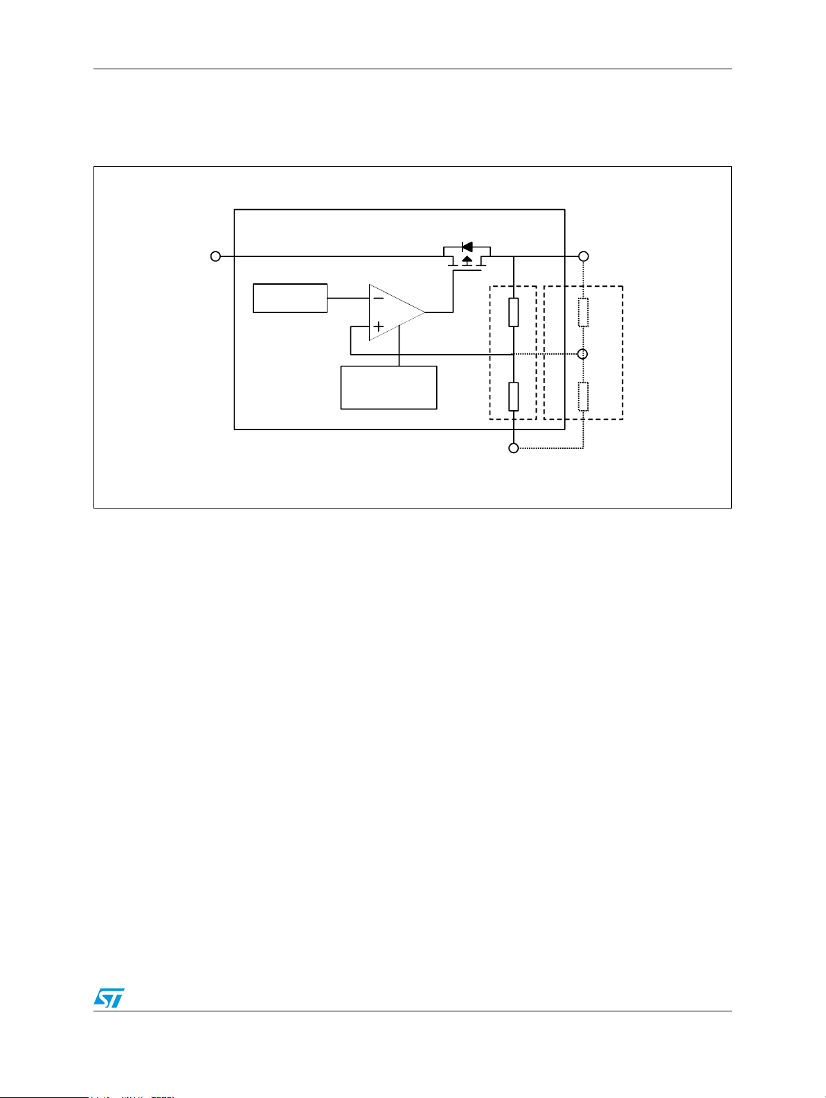
1 Diagram
Figure 1. Block diagram
Vin
V bandgap
1.22V
Vout
Adjustable
Fixed
ADJ
Short circuit &
thermal
protection
GND
3/18
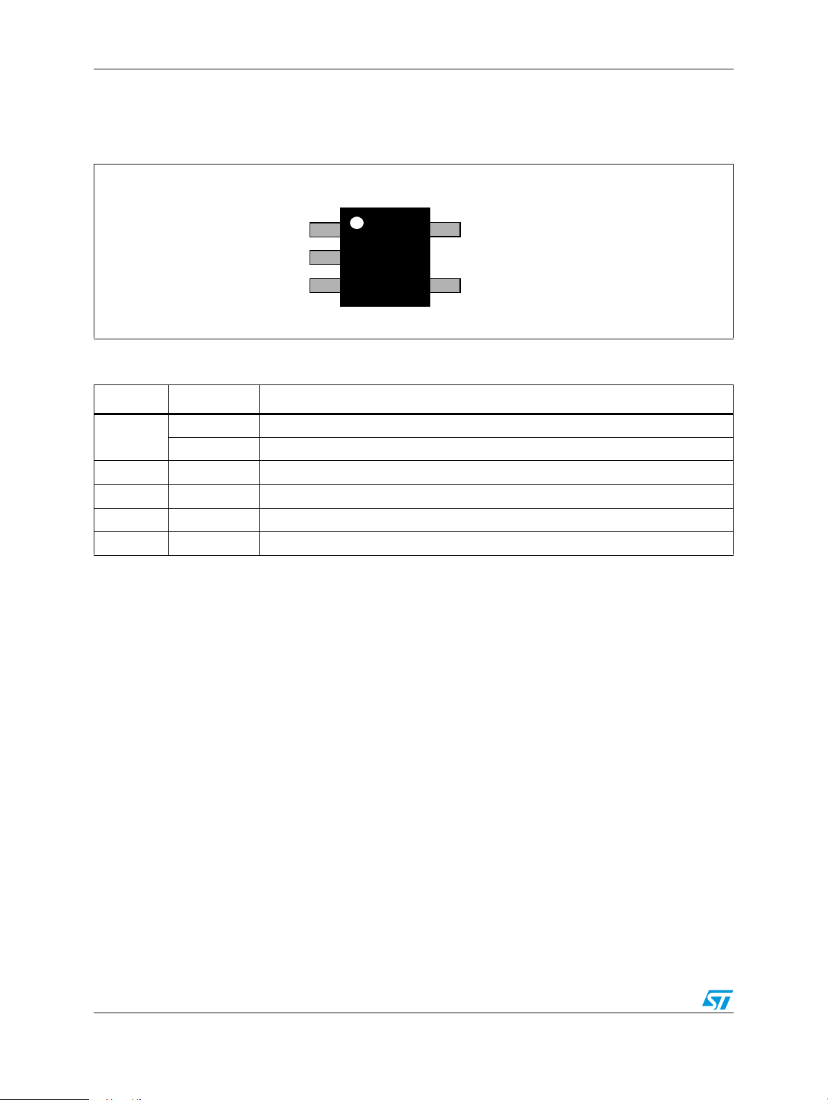
Pin configuration STLQ50XX
2 Pin configuration
Figure 2. Pin connections (top view)
ADJ
ADJ
STLQ50
GND
GND
N/C
N/C
Table 2. Pin description
Pin n° Symbol Note
1
2 GND Ground
3 N/C Not connected
4 IN Input voltage
5 OUT Output voltage
ADJ STLQ50: output voltage adjust
N/C STLQ50xx: not connected
STLQ50
OUT
OUT
IN
IN
4/18
STLQ50XX Maximum ratings
3 Maximum ratings
Table 3. Absolute maximum ratings
Symbol Parameter Value Unit
V
I
V
FB
DC Input voltage -0.3 to +14 V
FB voltage -0.3 to +7 V
ESD Human body model (all pins) ±2 kV
T
T
J
STG
Junction temperature -40 to 150 °C
Storage temperature range -55 to 150 °C
Note: Absolute maximum ratings are those values beyond which damage to the device may occur.
Functional operation under these conditions is not implied.
Table 4. Thermal data
Symbol Parameter SOT323-5L SOT23-5L Unit
R
thJA
1. This value is referred to a 4-layer PCB, JEDEC standard test board.
Thermal resistance junction-ambient 331.4
(1)
191
(1)
°C/W
5/18
Electrical characteristics STLQ50XX
4 Electrical characteristics
Table 5. Electrical characteristics
(V
= V
I
O(NOM)
are at T
Symbol Parameter Test conditions Min. Typ. Max. Unit
+1 V or VI = 2.5 V if VO + 1.5 V; TA= -40 °C to 125 °C; IO = 1 mA; typical values
= 25 °C, CO = 1 µF unless otherwise specified)
A
V
I
Q
Input voltage range
I
Quiescent current (Measured on
ground pin, fixed version)
=50mA 2.5 12
I
O
=5V 3.5 5.0
V
I
=12V 4.1 6.0
V
I
Output voltage range (STLQ50ADJ) 1.222 11 V
IO=20mA 2.3 12
V
O
Accuracy as percentage of nominal
=25°C
J
V
DROP-MAX
ΔV
ΔV
voltage at T
Max dropout voltage
Load regulation 1mA < IO <50mA 0.15 %/mA
O
Line regulation
O
SVR Supply voltage rejection
eN Output noise voltage
(1)
IO=50mA; 0.4 0.7 V
=1.5V:
V
O
VO+1V < VI <12V;
VO=1.5V:
2.5V < V
V
RIPPLE
<12V;
I
= 0.1V, IO= 20mA
f=120Hz
from 200Hz to
B
W
100KHZ; IO=10mA
-2 +2 %
30 dB
560 µV
Th Thermal protection 160 °C
I
OMAX
1. VI=2.5V when V
2. The maximum power dissipation must not be exceeded, see application information for details.
Maximum output current
≤ 2.1V
O(NOM)
(2)
VO=0V 500 mA
V
µA
0.3 %/V
RMS
6/18

STLQ50XX Typical application
5 Typical application
Figure 3. Fixed versions: STLQ5018- STLQ5025- STLQ5033- STLQ5050
Figure 4. Adjustable version STLQ50ADJ
7/18

Typical characteristics STLQ50XX
6 Typical characteristics
Figure 5. VO vs T
1.84
1.84
1.84
1.82
1.82
1.82
1.8
1.8
1.8
[V]
[V]
[V]
1.78
1.78
1.78
O
O
O
V
V
V
1.76
1.76
1.76
1.74
1.74
1.74
VI=2.8V, IO=20mA
VI=2.8V, IO=20mA
VI=2.8V, IO=20mA
1.72
1.72
1.72
-50 -25 0 25 50 75 100 125
-50 -25 0 25 50 75 100 125
-50 -25 0 25 50 75 100 125
Figure 7. IQ vs T
3.5
3.5
3.5
3.4
3.4
3.4
3.3
3.3
3.3
3.2
3.2
3.2
3.1
3.1
3.1
Iq [µA]
Iq [µA]
Iq [µA]
3
3
3
2.9
2.9
2.9
2.8
2.8
2.8
-50 -25 0 25 50 75 100 125
-50 -25 0 25 50 75 100 125
-50 -25 0 25 50 75 100 125
J
Temp [°C]
Temp [°C]
J
VI=5V, IO=1mA, VO=1.8V
VI=5V, IO=1mA, VO=1.8V
VI=5V, IO=1mA, VO=1.8V
Temp [°C]
Temp [°C]
Figure 6. VO vs V
2
2
1.8
1.8
1.6
1.6
1.4
1.4
1.2
1.2
[V]
[V]
1
1
O
O
V
V
0.8
0.8
0.6
0.6
0.4
0.4
0.2
0.2
0
0
0 12345
0 12345
Figure 8. V
0.5
0.5
0.45
0.45
0.4
0.4
0.35
0.35
[V]
[V]
0.3
0.3
0.25
0.25
DROP
DROP
V
V
0.2
0.2
0.15
0.15
0.1
0.1
0.05
0.05
0
0
DROP
0 102030 40 50
0 102030 40 50
I
vs I
O
VI[V]
VI[V]
IO[mA]
IO[mA]
IO=50mA, VO=1.8V
IO=50mA, VO=1.8V
TA=25°C
TA=25°C
Figure 9. V
0.7
0.7
0.6
0.6
0.5
0.5
[V]
[V]
0.4
0.4
0.3
0.3
DROP
DROP
V
V
0.2
0.2
0.1
0.1
0
0
-50 -25 0 25 50 75 100 125
-50 -25 0 25 50 75 100 125
DROP
vs T
J
VO=2.45V, IO=50mA
VO=2.45V, IO=50mA
Temp [°C]
Temp [°C]
8/18
Figure 10. Stability
12
12
11
11
10
10
9
9
8
8
7
7
6
6
5
5
ESR[ ]
ESR[ ]
4
4
3
3
2
2
1
1
0
0
0 12345
0 12345
CO[µF]
CO[µF]
TA=25°C
TA=25°C

STLQ50XX Typical characteristics
Figure 11. S.V.R. vs Freq. Figure 12. S.V.R. vs I
40
37
37
32
32
27
27
22
22
17
17
SVR [dB]
SVR [dB]
12
12
7
7
2
2
100 1000 10000 100000
100 1000 10000 100000
Frequency [Hz]
Frequency [Hz]
Figure 13. Line transient response Figure 14. Load transient response
VO=1.8V, IO=20mA
VO=1.8V, IO=20mA
40
38
38
36
36
34
34
32
32
30
30
28
28
SVR [dB]
SVR [dB]
26
26
24
24
22
22
20
20
0 1020304050
0 1020304050
O
IO[mA]
IO[mA]
VO=1.8V, f=120Hz
VO=1.8V, f=120Hz
IO=50mA; CO=10µF; VI=2.8V, VI rise/fall=5ms
Figure 15. Short circuit current Figure 16. Thermal protection
0.6
0.6
0.6
0.5
0.5
0.5
0.4
0.4
0.4
[A]
[A]
[A]
0.3
0.3
0.3
O
O
O
I
I
I
0.2
0.2
0.2
0.1
0.1
0.1
VO=0, TA=25°C
VO=0, TA=25°C
0
0
0
2 4 6 8 10 12 14
2 4 6 8 10 12 14
2 4 6 8 10 12 14
VI[V]
VI[V]
VO=0, TA=25°C
CO=1µF; VO=1.8V; VI=2.8V, Curr. rise/fall=1µs
2
2
1.75
1.75
1.5
1.5
1.25
1.25
[V]
[V]
1
1
O
O
V
V
0.75
0.75
0.5
0.5
0.25
0.25
0
0
155 157 159 161 163 165 167 169 171 173 175
155 157 159 161 163 165 167 169 171 173 175
[°C]
[°C]
T
T
J
J
VI=2.8V
VI=2.8V
9/18

Application information STLQ50XX
7 Application information
The STLQ50 is a BiCMOS linear regulator specifically designed for operating in
environment with very low power consumption constraints. The very low quiescent current
of 3 µA is obtained with use of CMOS technology that makes the device suitable for those
application that have very long stand-by time. The very low power consumption allows
extending the battery life and the tiny packages (SOT323-5L or SOT23-5L) fulfil the space
saving requirements of battery powered equipments. Moreover the STLQ50 provides wide
input voltage operation from 2.5 V up to 12 V.
The P-MOS pass element allows also a very good drop-out figure: 0.7 V at full load and at
125 °C without affecting the consumption characteristics.
7.1 External components
The typical application schematic of STLQ50 is shown in Figure 1 - Figure 2, a 1 µF input
and output capacitors placed close to the device are needed in order to provide proper
operation. The device is stable with electrolytic and ceramic output capacitors having values
higher than 1 µF (see figure typical characteristics for stability details).
In the adjustable version (STLQ50) the output voltage is programmed using an external
resistor divider as shown in Figure 2. The output voltage can be adjusted from 1.22 to 11 V
and it can be calculated using the following formula:
V
= VFB x (1+R1/R2)
O
where V
The sum between R
=1.222 V is the internal reference voltage;
FB
and R2 resistors should be chosen in order to guarantee 1 µA of
1
divider current at least. Lower value resistors will improve the noise performances but the
quiescent current will increase. Higher value resistors should be avoided because the ADJ
leakage current will influence the voltage set by the resistor divider making the above
formula no more valid.
The suggested design procedure is to choose R
following formula: R
= (VO/VFB-1) x R
1
7.2 Power dissipation
In order to ensure proper operation, the STLQ50 junction temperature should never exceed
125 °C, this limits the maximum power dissipation the regulator can sustain in any
application. The maximum power dissipation can be calculated as:
P
= (T
DMAX
where T
T
A
R
JMAX
is the ambient temperature;
is the junction to ambient thermal resistance of the package (seeTa bl e 4 thermal
thJA
data).
- TA)/R
JMAX
= 125 °C;
thJA
= 1 MΩ and then calculate R1 using the
2
2
10/18
The power dissipation can be calculated simply as:
P
= (VI - VO) x I
D
O
In every application condition, PD must be lower than P
DMAX
.

STLQ50XX Application information
7.3 Protection
The P-MOS pass element has an internal diode with anode connected to VO and cathode to
V
. In case VO > VI the current will flow from output to the input without any limitation. In this
I
case proper limiting network is recommended.
The current limitation is automatically provided by the characteristics of the PMOS pass
element (see typical characteristics), so the short circuit current is dependent on the input
voltage. When considering the short circuit current take care, in any case, to not exceed the
maximum power dissipation sustainable by the device.
The STLQ50 features an internal thermal protection that linearly reduces the output current
when the internal temperature increases, consequently, at a given load, also the output
voltage decreases. The action of the thermal protection starts at 125 °C when the output
voltage slightly decreases, while close to 163 °C the output voltage drops to 0 V. Since this
is a linear control, sudden over current conditions can quickly rise the chip temperature
without time for the thermal protection to act, so it cannot be used as a limitation for the
output current.
11/18

Package mechanical data STLQ50XX
8 Package mechanical data
In order to meet environmental requirements, ST offers these devices in ECOPACK®
packages. These packages have a lead-free second level interconnect. The category of
second Level Interconnect is marked on the package and on the inner box label, in
compliance with JEDEC Standard JESD97. The maximum ratings related to soldering
conditions are also marked on the inner box label. ECOPACK is an ST trademark.
ECOPACK specifications are available at: www.st.com.
12/18

STLQ50XX Package mechanical data
SOT323-5L mechanical data
mm. mils.
Dim.
Min. Typ. Max. Min. Typ. Max.
A0.80 1.10 31.5 43.3
A1 0.00 0.10 0.0 3.9
A2 0.80 1.00 31.5 39.4
b 0.15 0.305.9 11.8
C 0.10 0.183.9 7.1
D1.80 2.20 70.986.6
E1.80 2.40 70.994.5
E1 1.15 1.35 45.3 53.1
e 0.65 25.6
e1 1.3 51.2
L 0.10 0.30 3.9 11.8
13/18

Package mechanical data STLQ50XX
SOT23-5L mechanical data
mm. mils.
Dim.
Min. Typ. Max. Min. Typ. Max.
A0.90 1.45 35.4 57.1
A1 0.00 0.10 0.0 3.9
A2 0.901.30 35.4 51.2
b 0.35 0.50 13.7 19.7
C0.09 0.20 3.5 7.8
D2.80 3.00 110.2 118.1
E 1.50 1.75 59.0 68.8
e0.95 37.4
H 2.60 3.00 102.3 118.1
L 0.10 0.60 3.9 23.6
14/18
7049676D

STLQ50XX Package mechanical data
Tape & reel SOT323-xL mechanical data
Dim.
Min. Typ. Max. Min. Typ. Max.
A 175 1801856.889 7.086 7.283
C 12.8 13 13.2 0.504 0.512 0.519
D 20.2 0.795
N59.5 60 60.5 2.362
T 14.4 0.567
Ao 2.25 0.088
Bo 2.7 0.106
Ko 1.2 0.047
Po 3.9 4 4.1 0.153 0.157 0.161
P 3.8 4 4.2 0.149 0.157 0.165
mm. inch.
15/18

Package mechanical data STLQ50XX
Tape & reel SOT23-xL mechanical data
Dim.
Min. Typ. Max. Min. Typ. Max.
A180 7.086
C 12.8 13.0 13.2 0.504 0.512 0.519
D 20.2 0.795
N60 2.362
T 14.4 0.567
Ao 3.133.233.33 0.123 0.127 0.131
Bo 3.07 3.17 3.27 0.120 0.124 0.128
Ko 1.27 1.37 1.47 0.050 0.054 0.0.58
Po 3.9 4.0 4.1 0.153 0.157 0.161
P 3.9 4.0 4.1 0.153 0.157 0.161
mm. inch.
16/18

STLQ50XX Revision history
9 Revision history
Table 6. Document revision history
Date Revision Changes
07-Feb-2007 1 Initial release.
13-Feb-2007 2 Typo in cover page 350mA ==> 350mV.
06-Jul-2007 3 Added part number.
14-Nov-2007 4 Added Ta b le 1 .
17/18

STLQ50XX
Please Read Carefully:
Information in this document is provided solely in connection with ST products. STMicroelectronics NV and its subsidiaries (“ST”) reserve the
right to make changes, corrections, modifications or improvements, to this document, and the products and services described herein at any
time, without notice.
All ST products are sold pursuant to ST’s terms and conditions of sale.
Purchasers are solely responsible for the choice, selection and use of the ST products and services described herein, and ST assumes no
liability whatsoever relating to the choice, selection or use of the ST products and services described herein.
No license, express or implied, by estoppel or otherwise, to any intellectual property rights is granted under this document. If any part of this
document refers to any third party products or services it shall not be deemed a license grant by ST for the use of such third party products
or services, or any intellectual property contained therein or considered as a warranty covering the use in any manner whatsoever of such
third party products or services or any intellectual property contained therein.
UNLESS OTHERWISE SET FORTH IN ST’S TERMS AND CONDITIONS OF SALE ST DISCLAIMS ANY EXPRESS OR IMPLIED
WARRANTY WITH RESPECT TO THE USE AND/OR SALE OF ST PRODUCTS INCLUDING WITHOUT LIMITATION IMPLIED
WARRANTIES OF MERCHANTABILITY, FITNESS FOR A PARTICULAR PURPOSE (AND THEIR EQUIVALENTS UNDER THE LAWS
OF ANY JURISDICTION), OR INFRINGEMENT OF ANY PATENT, COPYRIGHT OR OTHER INTELLECTUAL PROPERTY RIGHT.
UNLESS EXPRESSLY APPROVED IN WRITING BY AN AUTHORIZED ST REPRESENTATIVE, ST PRODUCTS ARE NOT
RECOMMENDED, AUTHORIZED OR WARRANTED FOR USE IN MILITARY, AIR CRAFT, SPACE, LIFE SAVING, OR LIFE SUSTAINING
APPLICATIONS, NOR IN PRODUCTS OR SYSTEMS WHERE FAILURE OR MALFUNCTION MAY RESULT IN PERSONAL INJURY,
DEATH, OR SEVERE PROPERTY OR ENVIRONMENTAL DAMAGE. ST PRODUCTS WHICH ARE NOT SPECIFIED AS "AUTOMOTIVE
GRADE" MAY ONLY BE USED IN AUTOMOTIVE APPLICATIONS AT USER’S OWN RISK.
Resale of ST products with provisions different from the statements and/or technical features set forth in this document shall immediately void
any warranty granted by ST for the ST product or service described herein and shall not create or extend in any manner whatsoever, any
liability of ST.
ST and the ST logo are trademarks or registered trademarks of ST in various countries.
Information in this document supersedes and replaces all information previously supplied.
The ST logo is a registered trademark of STMicroelectronics. All other names are the property of their respective owners.
© 2007 STMicroelectronics - All rights reserved
STMicroelectronics group of companies
Australia - Belgium - Brazil - Canada - China - Czech Republic - Finland - France - Germany - Hong Kong - India - Israel - Italy - Japan -
Malaysia - Malta - Morocco - Singapore - Spain - Sweden - Switzerland - United Kingdom - United States of America
www.st.com
18/18
 Loading...