

Ultra-low current 2.4 V precision analog temperature sensor
Features
■ Precision analog voltage output temperature
sensor
■ ±1.5 °C maximum temperature accuracy
at 25 °C (±0.5 °C typical)
■ Ultra-low quiescent supply current:
4.8 µA (typ) and 8.0
■ Operating voltage range: 2.4 V to 5.5 V
■ Operating temperature range:
–55 °C to 130 °C (grade 7)
–40 °C to 85 °C (grade 9)
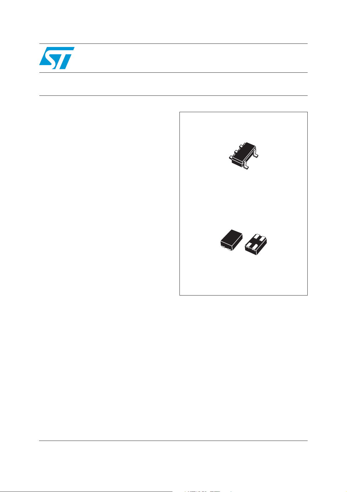
■ SOT323-5L 5-lead package
■ UDFN-4L 4-lead package
Applications
µA (max)
STLM20
SOT323-5L
■ Smartphones
■ Multimedia PDA devices
■ GPS devices
■ Portable medical instruments
■ Voltage-controlled crystal oscillator
temperature monitors
■ RF power transistor monitor
UDFN-4L
July 2010 Doc ID 12495 Rev 13 1/19
www.st.com
1

Contents STLM20
Contents
1 Description . . . . . . . . . . . . . . . . . . . . . . . . . . . . . . . . . . . . . . . . . . . . . . . . . 5
2 Transfer function . . . . . . . . . . . . . . . . . . . . . . . . . . . . . . . . . . . . . . . . . . . . 6
3 Maximum ratings . . . . . . . . . . . . . . . . . . . . . . . . . . . . . . . . . . . . . . . . . . . . 8
4 DC and AC characteristics . . . . . . . . . . . . . . . . . . . . . . . . . . . . . . . . . . . . 9
5 Capacitive load . . . . . . . . . . . . . . . . . . . . . . . . . . . . . . . . . . . . . . . . . . . . 10
6 Typical operating characteristics . . . . . . . . . . . . . . . . . . . . . . . . . . . . . 11
7 Package mechanical data . . . . . . . . . . . . . . . . . . . . . . . . . . . . . . . . . . . . 12
8 Part numbering . . . . . . . . . . . . . . . . . . . . . . . . . . . . . . . . . . . . . . . . . . . . 17
9 Revision history . . . . . . . . . . . . . . . . . . . . . . . . . . . . . . . . . . . . . . . . . . . 18
2/19 Doc ID 12495 Rev 13

STLM20 List of tables
List of tables
Table 1. Signal names . . . . . . . . . . . . . . . . . . . . . . . . . . . . . . . . . . . . . . . . . . . . . . . . . . . . . . . . . . . . 5
Table 2. First order equations optimized for different temperature ranges . . . . . . . . . . . . . . . . . . . . . 6
Table 3. Second order parabolic equation (V
Table 4. Second order parabolic equation for operation over the full voltage range
(V
= 2.4 V to 5.5 V) . . . . . . . . . . . . . . . . . . . . . . . . . . . . . . . . . . . . . . . . . . . . . . . . . . . . . . 7
Table 5. Absolute maximum ratings . . . . . . . . . . . . . . . . . . . . . . . . . . . . . . . . . . . . . . . . . . . . . . . . . . 8
Table 6. DC and AC characteristics . . . . . . . . . . . . . . . . . . . . . . . . . . . . . . . . . . . . . . . . . . . . . . . . . . 9
Table 7. Resistor/capacitor combinations for the filter network . . . . . . . . . . . . . . . . . . . . . . . . . . . . 10
Table 8. SOT323-5L – 5-lead small outline transistor package mechanical data. . . . . . . . . . . . . . . 13
Table 9. UDFN-4L – 4-lead (1.00 mm x 1.30 mm) package mechanical data . . . . . . . . . . . . . . . . . 14
Table 10. Carrier tape dimensions for SOT323-5L and UDFN-4L packages . . . . . . . . . . . . . . . . . . . 15
Table 11. Reel dimensions for 8 mm carrier tape - SOT323-5L and UDFN-4L packages . . . . . . . . . 16
Table 12. Ordering information scheme . . . . . . . . . . . . . . . . . . . . . . . . . . . . . . . . . . . . . . . . . . . . . . . 17
Table 13. Marking description. . . . . . . . . . . . . . . . . . . . . . . . . . . . . . . . . . . . . . . . . . . . . . . . . . . . . . . 17
Table 14. Document revision history . . . . . . . . . . . . . . . . . . . . . . . . . . . . . . . . . . . . . . . . . . . . . . . . . 18
CC
= 2.7 V) . . . . . . . . . . . . . . . . . . . . . . . . . . . . . . . . . . 7
CC
Doc ID 12495 Rev 13 3/19

List of figures STLM20
List of figures
Figure 1. Logic diagram . . . . . . . . . . . . . . . . . . . . . . . . . . . . . . . . . . . . . . . . . . . . . . . . . . . . . . . . . . . . 5
Figure 2. Connections (top view) . . . . . . . . . . . . . . . . . . . . . . . . . . . . . . . . . . . . . . . . . . . . . . . . . . . . . 5
Figure 3. Filter network for noisy environments or capacitive loads > 300 pF . . . . . . . . . . . . . . . . . . 10
Figure 4. V
Figure 5. SOT323-5L – 5-lead small outline transistor package outline . . . . . . . . . . . . . . . . . . . . . . 13
Figure 6. UDFN-4L – 4-lead (1.00 mm x 1.30 mm) package outline . . . . . . . . . . . . . . . . . . . . . . . . . 14
Figure 7. Carrier tape for SOT323-5L and UDFN-4L packages. . . . . . . . . . . . . . . . . . . . . . . . . . . . . 15
Figure 8. Reel schematic . . . . . . . . . . . . . . . . . . . . . . . . . . . . . . . . . . . . . . . . . . . . . . . . . . . . . . . . . . 16
vs. temperature . . . . . . . . . . . . . . . . . . . . . . . . . . . . . . . . . . . . . . . . . . . . . . . . . . . . . 11
OUT
4/19 Doc ID 12495 Rev 13
STLM20 Description
1 Description
The STLM20 is a precision analog output temperature sensor for low current applications
where maximizing battery life is important. It operates over a –55 °C to 130 °C (grade 7) or
–40 °C to 85 °C (grade 9) temperature range. The power supply operating range is 2.4 V to
5.5 V. The maximum temperature accuracy of the STLM20 is ± 1.5 °C (±0.5 °C typ) at an
ambient temperature of 25 °C and V
and reaches a maximum of ±2.5 °C at the temperature range extremes. The temperature
range is affected by the power supply voltage. For the temperature grade 7 device, a power
supply voltage of 2.7 V to 5.5 V, the temperature range extremes are +130 °C and –55 °C
(decreasing the power supply voltage from 2.7 V to 2.4 V changes the low end of the
operating temperature range from –55 °C to –30 °C, while the positive remains at +130 °C).
The STLM20 has a maximum quiescent supply current of 8 µA. Therefore, self-heating is
negligible.
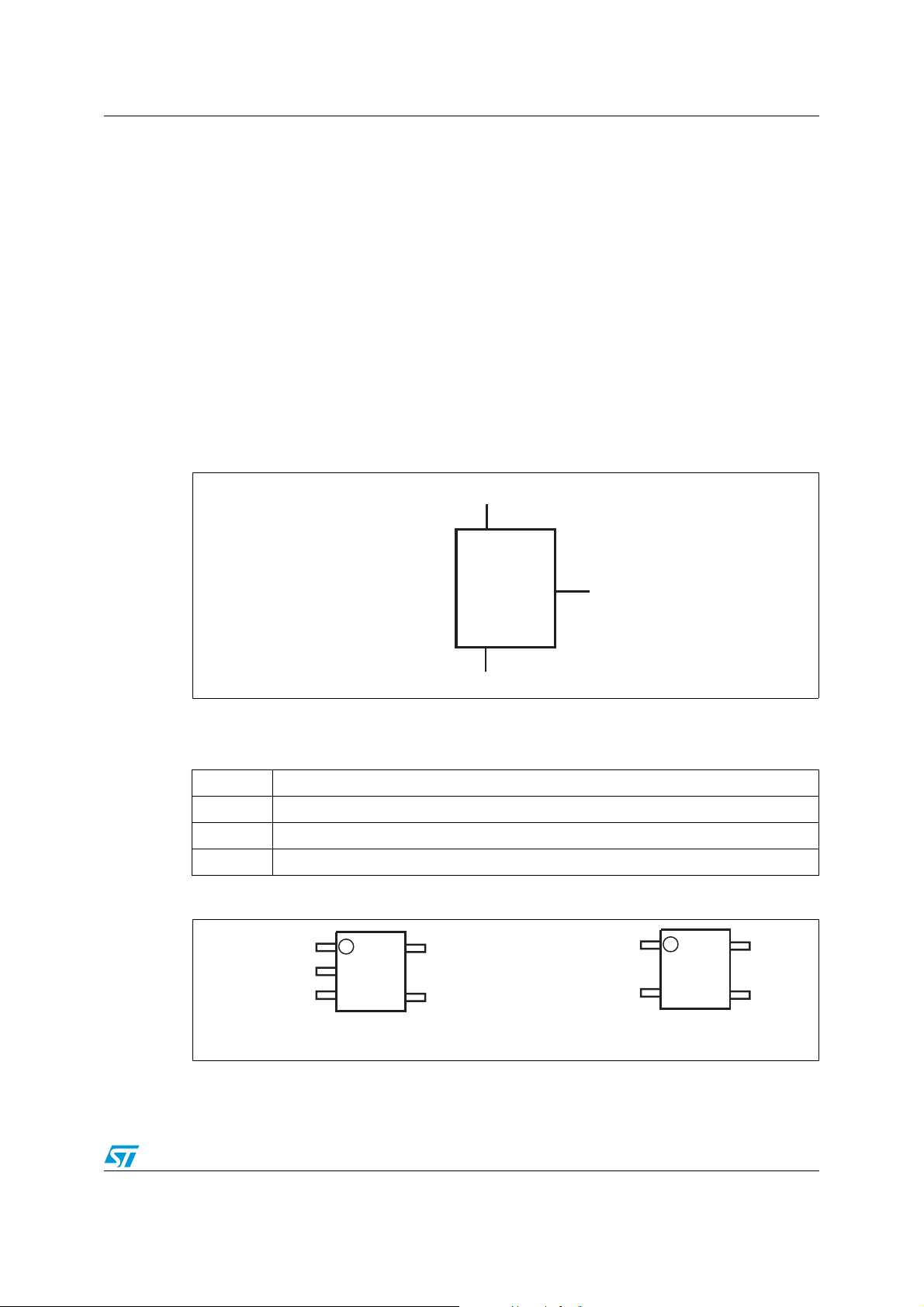
Figure 1. Logic diagram
of 2.7 V. The temperature error increases linearly
CC
V
CC
STLM20
(1)
GND
1. Pin 2 GND may be grounded or left floating (SOT323-5L only). For optimum thermal conductivity to the PC
board ground plane, it should be grounded.
Table 1. Signal names
V
CC
Supply voltage
V
OUT
AI12252
GND Ground
V
OUT
Output voltage
NC No connect
Figure 2. Connections (top view)
NC
GND
V
OUT
(1)
(2)
1
5
2
3
4
SOT323-5L
GND
V
CC
AI12253
V
NC
OUT
(1)
1
2
UDFN-4L
4
3
V
CC
GND
AI12253_a
1. Pin 1 NC should be left floating or grounded.
2. Pin 2 GND may be grounded or left floating. For optimum thermal conductivity to the PC board ground
plane, it should be grounded.
Doc ID 12495 Rev 13 5/19
Transfer function STLM20
2 Transfer function
The STLM20’s transfer function can be described in different ways, with varying levels of
precision. A simple linear transfer function, with good accuracy near 25 °C is expressed as:
Equation 1 (first order linear equation)
V
11.69m V–()°CT1.8663+×⁄ V=
O
Over the specified operating temperature range, the best accuracy can be obtained by using
the parabolic transfer function:
Equation 2 (second order parabolic equation)
O
−
2–26
8639.1)T1015.1(–)T1088.3(–V
+××+××=
and solving for T:
()
6
101962.296.1481–T
+×+=
V8639.1
−
O
6–
1088.3
×
The best fit linear transfer function for many popular temperature ranges was calculated in
Ta bl e 2 , where the error introduced by the linear transfer function increases with wider
temperature ranges.
Table 2. First order equations optimized for different temperature ranges
Temperature range
T
min
(°C) T
max
(°C)
Linear equation
VO =
Maximum deviation of linear
equation from parabolic equation
(°C)
–55 130 –11.79 mV/°C * T + 1.8528 V ±1.41
–40 110 –11.77 mV/°C * T + 1.8577 V ±0.93
–30 100 –11.77 mV/°C * T + 1.8605 V ±0.70
–40 85 –11.67 mV/°C * T + 1.8583 V ±0.65
–10 65 –11.71 mV/°C * T + 1.8641 V ±0.23
35 45 –11.81 mV/°C * T + 1.8701 V ±0.004
20 30 –11.69 mV/°C * T + 1.8663 V ±0.004
6/19 Doc ID 12495 Rev 13

STLM20 Transfer function
Table 3. Second order parabolic equation (VCC = 2.7 V)
Parameter Conditions Min Typ Max Unit
= –55 °C 2.457 2.485 2.512
T
A
T
= –40 °C 2.292 2.318 2.343
A
= –30 °C 2.181 2.205 2.230
T
A
T
= –20 °C 2.069 2.092 2.116
Temperature error based on:
= (–3.88 x 10⁻⁶ × T2) + (–1.15 x 10⁻² × T) +
V
OUT
1.8639 where T is the temperature
Table 4. Second order parabolic equation for operation over the full voltage range
(V
= 2.4 V to 5.5 V)
CC
Parameter
(1)
Temperature error based on:
= (–3.88 x 10⁻⁶ × T2) + (–1.15 x 10⁻² × T) +
V
OUT
1.8639, where T is the temperature
1. V
2. Valid for VCC min = 2.7 V.
3. Valid for temperature grade 7 only.
tolerance is ±4% (temperature grade 9 only).
OUT
A
= 0 °C 1.842 1.864 1.886
T
A
= 25 °C 1.556 1.574 1.592
T
A
T
= 50 °C 1.255 1.279 1.303
A
= 85 °C 0.833 0.859 0.884
T
A
= 130 °C 0.272 0.303 0.335
T
A
Conditions Min Max Unit
= –55 °C
T
A
T
= –40 °C
A
= –30 °C 2.180 2.249
T
A
T
= –20 °C 2.068 2.135
A
= 0 °C 1.841 1.904
T
A
= 25 °C 1.555 1.610
T
A
T
= 50 °C 1.254 1.322
A
= 85 °C 0.832 0.903
T
A
= 130 °C
T
A
(2)(3)
(2)
(3)
2.457 2.531
2.292 2.362
0.271 0.353
V
V
Doc ID 12495 Rev 13 7/19

Maximum ratings STLM20
3 Maximum ratings
Stressing the device above the rating listed in the absolute maximum ratings table may
cause permanent damage to the device. These are stress ratings only and operation of the
device at these or any other conditions above those indicated in the operating sections of
this specification is not implied. Exposure to absolute maximum rating conditions for
extended periods may affect device reliability.
Table 5. Absolute maximum ratings
Symbol Parameter Value Unit
T
T
SLD
V
T
J(max)
STG
V
CC
I
O
Storage temperature –65 to +150 °C
(1)
Lead solder temperature for 10 seconds 260 °C
Output voltage –0.3 to VCC + 0.3 V
O
Supply voltage –0.2 to 6.5 V
Output current 10 mA
Maximum junction temperature 150 °C
SOT323-5L 331.4 °C/W
θ
JA
T
A
1. Reflow at peak temperature of 260 °C. The time above 255 °C must not exceed 30 seconds.
2. Grade 7: STLM20W87F
Grade 9: STLM20DD9F
Thermal resistance
(2)
Ambient operating temperature
UDFN-4L 160.2 °C/W
Grade 7 –55 to 130 °C
Grade 9 –40 to 85 °C
8/19 Doc ID 12495 Rev 13

STLM20 DC and AC characteristics
4 DC and AC characteristics
This section summarizes the DC and AC characteristics of the device. The parameters in
the DC and AC characteristics table that follows are derived from tests performed under the
test conditions. Designers should check that the operating conditions in their circuit match
the operating conditions when relying on the quoted parameters.
Table 6. DC and AC characteristics
Sym Description Test condition
V
CC
V
O
I
Q
Supply voltage
(1)
= –30 °C to 130 °C 2.4 5.5 V
T
A
= –55 °C to 130 °C or
T
A
–40 °C to 85 °C
Min Typ
2.7 5.5 V
(2)
Max Unit
Output voltage TA = 0 °C 1.8639 V
= 125 °C to 130 °C ±2.5 °C
T
A
T
= 80 °C to 85 °C ±1.00 ±2.1 °C
Second order parabolic equation
Temperature to voltage error
(3)
VO = (–3.88 x 10⁻⁶ * T2) +
–2
(–1.15 x 10
* T) + 1.8639 V
A
= 25 °C to 30 °C ±0.5 ±1.5 °C
T
A
T
= 0 °C ±0.75 ±1.9 °C
A
= –40 °C ±2.3 °C
T
A
= –55 °C ±2.5 °C
T
A
Quiescent current 2.4 V ≤ VCC ≤ 5.5 V 4.8 8 µA
Sensor gain (temperature sensitivity
or average slope),
= –11.77 mV/°C * T + 1.860 V
V
O
–30 °C ≤ T
≤ 100 °C –11.4 –11.77 –12.2 mV/°C
A
Non-linearity –20 °C ≤ TA ≤ 80 °C ±0.4 %
ΔI
Change of quiescent current 2.4 V ≤ VCC ≤ 5.5 V 0.7 µA
Q
T
RegL Load regulation
RegI1
RegI2 5.0 V ≤ V
1. Valid for ambient operating temperature: TA = –55 to 130 °C or TA = –40 to 85 °C; VCC = 2.7 V (except where noted).
2. T
3. Accuracy is defined as the error between the measured and calculated output voltage at specified conditions of voltage,
4. Positive load currents flow out of the device (sourcing) and can typically be 16 µA. For negative load currents (sinking), the
5. Over the supply range of 2.4 to 5.5 V.
6. Measured at constant junction temperature, with pulse testing and low duty cycle. Output changes due to heating may be
Temperature coefficient of quiescent
CVO
current
I
Shutdown current VCC ≤ 0.8 V 0.02 µA
SD
Output impedance
Z
O
(6)
0 µA ≤ I
2.4 V ≤ V
Line regulation
= TA = 25 °C, unless otherwise noted under test condition.
J
current, and temperature.
device can sink less than 1 µA.
calculated by multiplying internal dissipation by thermal resistance.
≤ 16 µA
L
(4)(5)
≤ 5.0 V 3.3 mV/V
CC
≤ 5.5 V 11 mV
CC
–11 nA/°C
160 Ω
–2.5 mV
Doc ID 12495 Rev 13 9/19

Capacitive load STLM20
5 Capacitive load
The STLM20 will handle capacitive loads of up to 300 pF. Over the specified temperature
range, the STLM20 has a maximum output impedance of 160 Ω.
In a noisy environment, it may be advisable to add some filtering to minimize noise in the
output voltage. A 0.1 µF capacitor added between the supply voltage and ground is
recommended.
In an extremely noisy environment, it may be necessary to add a low-pass filter network to
the output of the device. A 1 µF capacitor, in addition to the output impedance of the device,
and a 200 Ω series resistor, will provide a low-pass filter that will pass the slow thermal time
constant of the STLM20, while filtering the higher frequency noise.
Figure 3. Filter network for noisy environments or capacitive loads > 300 pF
0.1µF
Bypass Capacitor
C
FILTER
R
FILTER
Table 7. Resistor/capacitor combinations for the filter network
GND
V
CC
5
1
R
FILTER
200 Ω 1 µF
470 Ω 0.1 µF
680 Ω 0.01 µF
1000 Ω 1000 pF
10 kΩ 100 pF
100 kΩ 10 pF
4
2
3
V
OUT
C
L
AI12259
C
FILTER
Bypass Capacitor
GND
C
FILTER
0.1µF
V
CC
5
1
4
2
3
V
OUT
R
FILTER
C
AI12260
L
10/19 Doc ID 12495 Rev 13

STLM20 Typical operating characteristics
6 Typical operating characteristics
The graph shown in Figure 4 represents V
Figure 4. V
vs. temperature
OUT
2.50
2.00
(V)
1.50
OUT
1.00
V
0.50
0.00
–50 –20 10 40 70 100 130
Typical (V
= 2.7V)
CC
according to temperature.
OUT
Temperature (°C)
ai13484
Doc ID 12495 Rev 13 11/19

Package mechanical data STLM20
7 Package mechanical data
In order to meet environmental requirements, ST offers these devices in different grades of
ECOPACK
specifications, grade definitions and product status are available at: www.st.com.
ECOPACK
®
packages, depending on their level of environmental compliance. ECOPACK®
®
is an ST trademark.
12/19 Doc ID 12495 Rev 13

STLM20 Package mechanical data
Figure 5. SOT323-5L – 5-lead small outline transistor package outline
7091413_E
1. Drawing is not to scale.
Table 8. SOT323-5L – 5-lead small outline transistor package mechanical data
mm inches
Symbol
Typ Min Max Typ Min Max
A – 0.80 1.10 – 0.031 0.043
A1 – 0 0.10 – 0.000 0.004
A2 0.90 0.80 1.00 0.035 0.031 0.039
b – 0.15 0.30 – 0.006 0.012
c – 0.10 0.22 – 0.004 0.009
D 2.00 1.80 2.20 0.079 0.071 0.087
E 2.10 1.80 2.40 0.083 0.071 0.094
E1 1.25 1.15 1.35 0.049 0.045 0.053
e0.65– –0.026– –
e1 1.30 – – 0.051 – –
L 0.36 0.26 0.46 0.014 0.010 0.018
< – 0° 8° – 0° 8°
Doc ID 12495 Rev 13 13/19

Package mechanical data STLM20
Figure 6. UDFN-4L – 4-lead (1.00 mm x 1.30 mm) package outline
7986858
Note: Drawing is not to scale.
Table 9. UDFN-4L – 4-lead (1.00 mm x 1.30 mm) package mechanical data
Symbol
ddd 0 0.04 0.08 0 0.0016 0.0031
mm inches
Min Typ Max Min Typ Max
A 0.45 0.50 0.55 0.018 0.020 0.022
A1 0 0.025 0.05 0 0.001 0.002
A3 0.119 0.127 0.177 0.0046 0.0050 0.0069
b 0.20 0.25 0.30 0.008 0.010 0.012
D 0.95 1.00 1.05 0.037 0.039 0.041
E 1.25 1.30 1.35 0.049 0.051 0.053
e 0.45 0.50 0.55 0.018 0.020 0.022
L 0.35 0.40 0.45 0.014 0.016 0.018
L1 0.45 0.50 0.55 0.018 0.020 0.022
14/19 Doc ID 12495 Rev 13

STLM20 Package mechanical data
Figure 7. Carrier tape for SOT323-5L and UDFN-4L packages
P
D
T
A
TOP COVER
TAPE
K
0
0
CENTER LINES
OF CAVITY
P
2
B
0
0
P
1
E
F
W
USER DIRECTION OF FEED
Table 10. Carrier tape dimensions for SOT323-5L and UDFN-4L packages
Package W D E P
SOT323-5L
UDFN-4L
8.00
+0.30
–0.10
8.00
+0.30
–0.10
1.50
+0.10/
–0.00
1.50
+0.10/
–0.00
1.75
±0.10
1.75
±0.10
4.00
±0.10
4.00
±0.10
P
0
2.00
±0.10
2.00
±0.10
FA0B
2
3.50
±0.05
3.50
±0.05
2.25
±0.10
1.25
±0.10
0
2.40
±0.10
1.55
±0.10
K
0
1.22
±0.10
0.65
±0.05
P
1
4.00
±0.10
4.00
±0.10
AM03073v1
TUnit
0.30
±0.05
0.250
±0.05
mm 3000
mm 3000
Bulk
Qty
Doc ID 12495 Rev 13 15/19

Package mechanical data STLM20
Figure 8. Reel schematic
T
40mm min.
Access hole
At slot location
B
D
C
A
Tape slot
Full ra dius
In core for
Tape s tart
2.5mm min.width
N
G measured
At hub
AM04928v1
Table 11. Reel dimensions for 8 mm carrier tape - SOT323-5L and UDFN-4L packages
A
(max)
180 mm
(7-inch)
B
(min)
1.5 mm
C
13 mm
± 0.2 mm
D
(min)
N
(min)
20.2 mm 60 mm
G
8.4 mm
+ 2/–0 mm
T
(max)
14.4 mm
Note: The dimensions given in Tab l e 1 1 incorporate tolerances that cover all variations on critical
parameters.
16/19 Doc ID 12495 Rev 13

STLM20 Part numbering
8 Part numbering
Table 12. Ordering information scheme
Example: STLM20 DD 9 F
Device type
STLM20
Package
W8 = SOT323-5L
DD= UDFN-4L - ultra-thin DFN 4-lead
Temperature range
7 = –55 to 130°C
9 = –40 to 85°C
(1)(2)
(3)
Shipping method
®
F = ECOPACK
1. Available in temperature grade 7 (–55 to 130 °C) only
2. SOT323-5L also referred to as SC70-5L
3. Available in temperature grade 9 (–40 to 85 °C) only
package, tape & reel
Table 13. Marking description
Part number Package Marking
STLM20W87F SOT323-5L M20
STLM20DD9F UDFN-4L 20
For other options, or for more information on any aspect of this device, please contact the
ST sales office nearest you.
Doc ID 12495 Rev 13 17/19

Revision history STLM20
9 Revision history
Table 14. Document revision history
Date Revision Changes
28-Jun-2006 1 Initial release.
19-Jul-2006 2 Added Table 13: Marking description
Added a footnote concerning package availability in Features on
28-Aug-2006 3
05-Sep-2006 4
page 1 and to Ta bl e 1 2 and Tab l e 13; updated package mechanical
data in Ta bl e 9
Amended text in the Features on page 1, Section 1: Description,
Section 2: Transfer function, Ta bl e 6 , and Ta bl e 1 2 to elucidate that
two packages exist each with specific temperature ranges: SOT323-5
(SC70-5) 5-lead package (–55 to 130 °C) and UDFN 4-lead package
(–40 to 85 °C)
25-Sep-2006 5
Updated operating temperature ranges (now 7 and 9); updated
Table 6: DC and AC characteristics
Table 3: Second order parabolic equation (V
= 2.7 V) and Ta ble 4 :
CC
Second order parabolic equation for operation over the full voltage
10-Oct-2006 6
range (VCC = 2.4 V to 5.5 V) added. Section 6: Typical operating
characteristics added.
added to Table 5: Absolute maximum ratings.
T
A
Document status updated to full datasheet; updated text in the title of
04-Dec-2006 7
Table 4: Second order parabolic equation for operation over the full
voltage range (V
= 2.4 V to 5.5 V); added footnotes regarding
CC
temperature ranges in Table 12: Ordering information scheme.
08-Feb-2007 8 Added thermal resistance in Table 5: Absolute maximum ratings.
09-May-2007 9 Modified Equation 1, 2.
26-Nov-2007 10 Updated footnote 2 in Ta b l e 5; minor text updates.
Updated Figure 6: UDFN-4L – 4-lead (1.00 mm x 1.30 mm) package
07-Nov-2008 11
outline to reflect location of pin 1 with respect to the orientation of the
topside marking; updated Figure 5, Ta b l e 5 , 8, 12.
Updated Ta bl e 5 , text in Section 7: Package mechanical data; added
10-Sep-2009 12
tape and reel specifications (Figure 7 and Ta b l e 1 0); reformatted
document.
Updated Features, Section 1: Description, Section 2: Transfer
09-Jul-2010 13
function, Ta bl e 5 , 6, 12; added reel information (Figure 8, Ta bl e 1 1);
removed references to SC70-5L package; minor textual changes.
18/19 Doc ID 12495 Rev 13

STLM20
Please Read Carefully:
Information in this document is provided solely in connection with ST products. STMicroelectronics NV and its subsidiaries (“ST”) reserve the
right to make changes, corrections, modifications or improvements, to this document, and the products and services described herein at any
time, without notice.
All ST products are sold pursuant to ST’s terms and conditions of sale.
Purchasers are solely responsible for the choice, selection and use of the ST products and services described herein, and ST assumes no
liability whatsoever relating to the choice, selection or use of the ST products and services described herein.
No license, express or implied, by estoppel or otherwise, to any intellectual property rights is granted under this document. If any part of this
document refers to any third party products or services it shall not be deemed a license grant by ST for the use of such third party products
or services, or any intellectual property contained therein or considered as a warranty covering the use in any manner whatsoever of such
third party products or services or any intellectual property contained therein.
UNLESS OTHERWISE SET FORTH IN ST’S TERMS AND CONDITIONS OF SALE ST DISCLAIMS ANY EXPRESS OR IMPLIED
WARRANTY WITH RESPECT TO THE USE AND/OR SALE OF ST PRODUCTS INCLUDING WITHOUT LIMITATION IMPLIED
WARRANTIES OF MERCHANTABILITY, FITNESS FOR A PARTICULAR PURPOSE (AND THEIR EQUIVALENTS UNDER THE LAWS
OF ANY JURISDICTION), OR INFRINGEMENT OF ANY PATENT, COPYRIGHT OR OTHER INTELLECTUAL PROPERTY RIGHT.
UNLESS EXPRESSLY APPROVED IN WRITING BY AN AUTHORIZED ST REPRESENTATIVE, ST PRODUCTS ARE NOT
RECOMMENDED, AUTHORIZED OR WARRANTED FOR USE IN MILITARY, AIR CRAFT, SPACE, LIFE SAVING, OR LIFE SUSTAINING
APPLICATIONS, NOR IN PRODUCTS OR SYSTEMS WHERE FAILURE OR MALFUNCTION MAY RESULT IN PERSONAL INJURY,
DEATH, OR SEVERE PROPERTY OR ENVIRONMENTAL DAMAGE. ST PRODUCTS WHICH ARE NOT SPECIFIED AS "AUTOMOTIVE
GRADE" MAY ONLY BE USED IN AUTOMOTIVE APPLICATIONS AT USER’S OWN RISK.
Resale of ST products with provisions different from the statements and/or technical features set forth in this document shall immediately void
any warranty granted by ST for the ST product or service described herein and shall not create or extend in any manner whatsoever, any
liability of ST.
ST and the ST logo are trademarks or registered trademarks of ST in various countries.
Information in this document supersedes and replaces all information previously supplied.
The ST logo is a registered trademark of STMicroelectronics. All other names are the property of their respective owners.
© 2010 STMicroelectronics - All rights reserved
STMicroelectronics group of companies
Australia - Belgium - Brazil - Canada - China - Czech Republic - Finland - France - Germany - Hong Kong - India - Israel - Italy - Japan -
Malaysia - Malta - Morocco - Philippines - Singapore - Spain - Sweden - Switzerland - United Kingdom - United States of America
www.st.com
Doc ID 12495 Rev 13 19/19
 Loading...