


I²C interfaced, advanced LED controller/driver with keyscan,
standby power management and real time clock (RTC)
Features
■ LED controller driver with 13 outputs
(8 segments/5 digits)
■ Standby power management to host
■ Integrated low-power, accurate RTC
■ Integrated remote control decoding:
– Philips (RC5, RCMM)
– Thomson (RCA, R2000)
– NEC and R-STEP
■ Wake-up using front panel keys, remote
control, real time clock (RTC), extra pin (AV or
CEC)
■ Battery or super-cap back up mode for real
time clock (RTC)
■ Keyscanning (8x2 matrix)
■ Low power consumption in standby mode
2
■ I
C serial bus interface (SCL, SDA)
■ 16-step dimming circuit to control the display
brightness
■ 5.0 V (± 10%) for V
■
Built-in thermal protection circuit
■ External crystal with internal oscillator for real
time clock (RTC)
Applications
■ Set-top boxes
■ White goods
■ Home appliances
■ DVD players, VCRs, DVD-R
CC
STLED325
QFN32
(5 x 5 mm)
Description
The STLED325 is a compact LED controller/
driver that interfaces microprocessors to LED
displays through serial I
LEDs connected in common anode configuration
and includes keyscanning for an 8 x 2 key matrix
which automatically scans and de-bounces a
matrix of up to 16 switches.
Furthermore, the STLED325 provides standby
power management to the host. It also integrates
a low-power, highly-accurate RTC and a remotecontrol decoder. All functions are programmable
using the I
2
C bus. Low power consumption during
standby mode is achieved.
The STLED325 controller/driver is ideal as a
single peripheral device to interface the front
panel display with a single-chip host IC like CPU.
2
C interface. It drives
Table 1. Device summary
Order code Temp range (°C) Package Comments
STLED325QTR -40 to +85 °C QFN32 250 parts per reel
April 2011 Doc ID 17576 Rev 1 1/62
www.st.com
62

Contents STLED325
Contents
1 Description . . . . . . . . . . . . . . . . . . . . . . . . . . . . . . . . . . . . . . . . . . . . . . . . . 7
2 Functional and application diagram . . . . . . . . . . . . . . . . . . . . . . . . . . . . 8
3 Functional description . . . . . . . . . . . . . . . . . . . . . . . . . . . . . . . . . . . . . . 11
3.1 Low power mode of operation . . . . . . . . . . . . . . . . . . . . . . . . . . . . . . . . . 11
3.2 I2C serial interface . . . . . . . . . . . . . . . . . . . . . . . . . . . . . . . . . . . . . . . . . . 11
3.3 Initial power up . . . . . . . . . . . . . . . . . . . . . . . . . . . . . . . . . . . . . . . . . . . . . 11
3.4 Display types . . . . . . . . . . . . . . . . . . . . . . . . . . . . . . . . . . . . . . . . . . . . . . 12
3.5 Keyscan . . . . . . . . . . . . . . . . . . . . . . . . . . . . . . . . . . . . . . . . . . . . . . . . . . 12
3.6 Timers . . . . . . . . . . . . . . . . . . . . . . . . . . . . . . . . . . . . . . . . . . . . . . . . . . . 12
3.6.1 Guard timer . . . . . . . . . . . . . . . . . . . . . . . . . . . . . . . . . . . . . . . . . . . . . . 12
3.6.2 Watchdog timer . . . . . . . . . . . . . . . . . . . . . . . . . . . . . . . . . . . . . . . . . . . 13
3.7 Power-on-reset and soft-start . . . . . . . . . . . . . . . . . . . . . . . . . . . . . . . . . . 13
3.8 LED drivers . . . . . . . . . . . . . . . . . . . . . . . . . . . . . . . . . . . . . . . . . . . . . . . . 14
3.9 Over temperature cut-off . . . . . . . . . . . . . . . . . . . . . . . . . . . . . . . . . . . . . 14
3.10 Standby mode . . . . . . . . . . . . . . . . . . . . . . . . . . . . . . . . . . . . . . . . . . . . . 14
3.10.1 Cold boot up . . . . . . . . . . . . . . . . . . . . . . . . . . . . . . . . . . . . . . . . . . . . . 15
3.10.2 Entering standby mode . . . . . . . . . . . . . . . . . . . . . . . . . . . . . . . . . . . . . 17
3.10.3 Wake-up . . . . . . . . . . . . . . . . . . . . . . . . . . . . . . . . . . . . . . . . . . . . . . . . . 18
3.11 Real time clock (RTC) . . . . . . . . . . . . . . . . . . . . . . . . . . . . . . . . . . . . . . . 19
3.11.1 Reading the real time clock . . . . . . . . . . . . . . . . . . . . . . . . . . . . . . . . . . 19
3.11.2 Writing to the real time clock . . . . . . . . . . . . . . . . . . . . . . . . . . . . . . . . . 20
3.11.3 Register table for RTC . . . . . . . . . . . . . . . . . . . . . . . . . . . . . . . . . . . . . . 20
3.11.4 Setting alarm clock registers . . . . . . . . . . . . . . . . . . . . . . . . . . . . . . . . . 21
3.11.5 Century bits . . . . . . . . . . . . . . . . . . . . . . . . . . . . . . . . . . . . . . . . . . . . . . 22
3.11.6 Initial power-on defaults . . . . . . . . . . . . . . . . . . . . . . . . . . . . . . . . . . . . . 23
3.11.7 Programmable display . . . . . . . . . . . . . . . . . . . . . . . . . . . . . . . . . . . . . . 24
3.11.8 Lookup table with ppm against the calibration register values . . . . . . . . 24
3.12 Remote control decoder . . . . . . . . . . . . . . . . . . . . . . . . . . . . . . . . . . . . . . 26
3.13 Interrupt . . . . . . . . . . . . . . . . . . . . . . . . . . . . . . . . . . . . . . . . . . . . . . . . . . 26
3.14 Ready . . . . . . . . . . . . . . . . . . . . . . . . . . . . . . . . . . . . . . . . . . . . . . . . . . . . 27
3.15 Mute . . . . . . . . . . . . . . . . . . . . . . . . . . . . . . . . . . . . . . . . . . . . . . . . . . . . . 27
2/62 Doc ID 17576 Rev 1

STLED325 Contents
3.16 GPIO . . . . . . . . . . . . . . . . . . . . . . . . . . . . . . . . . . . . . . . . . . . . . . . . . . . . 27
3.17 Power sense circuits . . . . . . . . . . . . . . . . . . . . . . . . . . . . . . . . . . . . . . . . . 27
3.17.1 Switchover . . . . . . . . . . . . . . . . . . . . . . . . . . . . . . . . . . . . . . . . . . . . . . . 29
3.17.2 Battery low warning . . . . . . . . . . . . . . . . . . . . . . . . . . . . . . . . . . . . . . . . 30
3.17.3 Different power operation modes . . . . . . . . . . . . . . . . . . . . . . . . . . . . . . 30
3.18 Bus characteristics . . . . . . . . . . . . . . . . . . . . . . . . . . . . . . . . . . . . . . . . . . 31
4 Electrical ratings . . . . . . . . . . . . . . . . . . . . . . . . . . . . . . . . . . . . . . . . . . . 33
4.1 Absolute maximum ratings (TA = 25 °C, GND = 0 V) . . . . . . . . . . . . . . . . 33
4.2 Recommended operating conditions . . . . . . . . . . . . . . . . . . . . . . . . . . . . 34
4.2.1 DC electrical characteristics . . . . . . . . . . . . . . . . . . . . . . . . . . . . . . . . . 34
4.3 Power consumption estimation . . . . . . . . . . . . . . . . . . . . . . . . . . . . . . . . . 35
4.4 Oscillator and crystal characteristics . . . . . . . . . . . . . . . . . . . . . . . . . . . . 38
4.5 ESD performance . . . . . . . . . . . . . . . . . . . . . . . . . . . . . . . . . . . . . . . . . . . 39
5 Display RAM address and display mode . . . . . . . . . . . . . . . . . . . . . . . 41
6 KEY matrix and key-input data storage RAM . . . . . . . . . . . . . . . . . . . . 42
7 Commands . . . . . . . . . . . . . . . . . . . . . . . . . . . . . . . . . . . . . . . . . . . . . . . . 43
7.1 Configuration mode setting command . . . . . . . . . . . . . . . . . . . . . . . . . . . 43
7.2 Data setting command . . . . . . . . . . . . . . . . . . . . . . . . . . . . . . . . . . . . . . . 46
7.3 Configuration data . . . . . . . . . . . . . . . . . . . . . . . . . . . . . . . . . . . . . . . . . . 48
7.3.1 Interrupt flags . . . . . . . . . . . . . . . . . . . . . . . . . . . . . . . . . . . . . . . . . . . . . 49
7.4 Address setting command . . . . . . . . . . . . . . . . . . . . . . . . . . . . . . . . . . . . 50
7.5 Display control and hotkey setting command . . . . . . . . . . . . . . . . . . . . . . 51
7.6 Keyscanning and display timing . . . . . . . . . . . . . . . . . . . . . . . . . . . . . . . . 53
8 State . . . . . . . . . . . . . . . . . . . . . . . . . . . . . . . . . . . . . . . . . . . . . . . . . . . . . 54
8.1 Default state upon power-up . . . . . . . . . . . . . . . . . . . . . . . . . . . . . . . . . . 54
8.2 Initial state . . . . . . . . . . . . . . . . . . . . . . . . . . . . . . . . . . . . . . . . . . . . . . . . 54
9 Remote control protocols . . . . . . . . . . . . . . . . . . . . . . . . . . . . . . . . . . . . 55
10 Application information . . . . . . . . . . . . . . . . . . . . . . . . . . . . . . . . . . . . . 56
10.1 Power supply sequencing . . . . . . . . . . . . . . . . . . . . . . . . . . . . . . . . . . . . . 56
Doc ID 17576 Rev 1 3/62

Contents STLED325
10.2 ISET variation with RSET . . . . . . . . . . . . . . . . . . . . . . . . . . . . . . . . . . . . . 56
10.3 Application diagram . . . . . . . . . . . . . . . . . . . . . . . . . . . . . . . . . . . . . . . . . 57
11 Package mechanical data . . . . . . . . . . . . . . . . . . . . . . . . . . . . . . . . . . . . 58
12 Revision history . . . . . . . . . . . . . . . . . . . . . . . . . . . . . . . . . . . . . . . . . . . 61
4/62 Doc ID 17576 Rev 1

STLED325 List of tables
List of tables
Table 1. Device summary . . . . . . . . . . . . . . . . . . . . . . . . . . . . . . . . . . . . . . . . . . . . . . . . . . . . . . . . . . 1
Table 2. Register table for RTC . . . . . . . . . . . . . . . . . . . . . . . . . . . . . . . . . . . . . . . . . . . . . . . . . . . . 20
Table 3. Alarm repeat modes . . . . . . . . . . . . . . . . . . . . . . . . . . . . . . . . . . . . . . . . . . . . . . . . . . . . . . 22
Table 4. Century bits examples . . . . . . . . . . . . . . . . . . . . . . . . . . . . . . . . . . . . . . . . . . . . . . . . . . . . 22
Table 5. Initial power-on defaults . . . . . . . . . . . . . . . . . . . . . . . . . . . . . . . . . . . . . . . . . . . . . . . . . . . 23
Table 6. RTC display . . . . . . . . . . . . . . . . . . . . . . . . . . . . . . . . . . . . . . . . . . . . . . . . . . . . . . . . . . . . 24
Table 7. LUT with ppm against the calibration register values . . . . . . . . . . . . . . . . . . . . . . . . . . . . . 24
Table 8. Different power operation modes . . . . . . . . . . . . . . . . . . . . . . . . . . . . . . . . . . . . . . . . . . . . 30
Table 9. Pin description . . . . . . . . . . . . . . . . . . . . . . . . . . . . . . . . . . . . . . . . . . . . . . . . . . . . . . . . . . 32
Table 10. Absolute maximum ratings (TA = 25 °C, GND = 0 V) . . . . . . . . . . . . . . . . . . . . . . . . . . . . . 33
Table 11. Thermal data. . . . . . . . . . . . . . . . . . . . . . . . . . . . . . . . . . . . . . . . . . . . . . . . . . . . . . . . . . . . 33
Table 12. DC electrical characteristics . . . . . . . . . . . . . . . . . . . . . . . . . . . . . . . . . . . . . . . . . . . . . . . . 34
Table 13. Voltage drop estimation with RGB LED . . . . . . . . . . . . . . . . . . . . . . . . . . . . . . . . . . . . . . . 35
Table 14. Capacitance (TA = 25°C, f = 1 MHz) . . . . . . . . . . . . . . . . . . . . . . . . . . . . . . . . . . . . . . . . . 35
Table 15. Power supply characteristics (TA = -40 to 85°C) . . . . . . . . . . . . . . . . . . . . . . . . . . . . . . . . 36
Table 16. Dynamic switching characteristics (TA = -40 to +85 °C, VCC = 5.0V ± 10%, GND=0.0V, Typ-
ical values are at 25°C). . . . . . . . . . . . . . . . . . . . . . . . . . . . . . . . . . . . . . . . . . . . . . . . . . . . 36
Table 17. Timing characteristics (TA = -40 to +85 °C, VCC = 5.0 V ± 10%, GND=0.0 V, typical values
are at 25 °C) . . . . . . . . . . . . . . . . . . . . . . . . . . . . . . . . . . . . . . . . . . . . . . . . . . . . . . . . . . . . 37
Table 18. Oscillator characteristics . . . . . . . . . . . . . . . . . . . . . . . . . . . . . . . . . . . . . . . . . . . . . . . . . . . 38
Table 19. Crystal electrical characteristics . . . . . . . . . . . . . . . . . . . . . . . . . . . . . . . . . . . . . . . . . . . . . 38
Table 20. ESD performance . . . . . . . . . . . . . . . . . . . . . . . . . . . . . . . . . . . . . . . . . . . . . . . . . . . . . . . . 39
Table 21. Battery range and battery detect . . . . . . . . . . . . . . . . . . . . . . . . . . . . . . . . . . . . . . . . . . . . 39
Table 22. Power down/up AC characteristics . . . . . . . . . . . . . . . . . . . . . . . . . . . . . . . . . . . . . . . . . . . 39
Table 23. Power down/up trip points DC characteristics . . . . . . . . . . . . . . . . . . . . . . . . . . . . . . . . . . 39
Table 24. Thermal shutdown characteristics . . . . . . . . . . . . . . . . . . . . . . . . . . . . . . . . . . . . . . . . . . . 40
Table 25. Bit map for segment 1 to segment 8 . . . . . . . . . . . . . . . . . . . . . . . . . . . . . . . . . . . . . . . . . . 41
Table 26. Data write command. b5 b4: 00 . . . . . . . . . . . . . . . . . . . . . . . . . . . . . . . . . . . . . . . . . . . . . 46
Table 27. Data Write 2 command. B5 b4: 01 . . . . . . . . . . . . . . . . . . . . . . . . . . . . . . . . . . . . . . . . . . . 47
Table 28. Data Read 1 command. b5 b4: 10 . . . . . . . . . . . . . . . . . . . . . . . . . . . . . . . . . . . . . . . . . . . 47
Table 29. Data Read 2 command. b5 b4: 11 . . . . . . . . . . . . . . . . . . . . . . . . . . . . . . . . . . . . . . . . . . . 47
Table 30. Power-up defaults. . . . . . . . . . . . . . . . . . . . . . . . . . . . . . . . . . . . . . . . . . . . . . . . . . . . . . . . 54
Table 31. QFN32 (5 x 5 mm) mechanical data . . . . . . . . . . . . . . . . . . . . . . . . . . . . . . . . . . . . . . . . . . 58
Table 32. Document revision history . . . . . . . . . . . . . . . . . . . . . . . . . . . . . . . . . . . . . . . . . . . . . . . . . 61
Doc ID 17576 Rev 1 5/62

List of figures STLED325
List of figures
Figure 1. Functional block diagram . . . . . . . . . . . . . . . . . . . . . . . . . . . . . . . . . . . . . . . . . . . . . . . . . . . 8
Figure 2. Application diagram . . . . . . . . . . . . . . . . . . . . . . . . . . . . . . . . . . . . . . . . . . . . . . . . . . . . . . . 9
Figure 3. Pin configurations . . . . . . . . . . . . . . . . . . . . . . . . . . . . . . . . . . . . . . . . . . . . . . . . . . . . . . . . 10
Figure 4. Display types . . . . . . . . . . . . . . . . . . . . . . . . . . . . . . . . . . . . . . . . . . . . . . . . . . . . . . . . . . . 12
Figure 5. Power-up condition . . . . . . . . . . . . . . . . . . . . . . . . . . . . . . . . . . . . . . . . . . . . . . . . . . . . . . . 16
Figure 6. Power down condition (normal behavior) . . . . . . . . . . . . . . . . . . . . . . . . . . . . . . . . . . . . . . 17
Figure 7. Standby condition (normal behavior) . . . . . . . . . . . . . . . . . . . . . . . . . . . . . . . . . . . . . . . . . 18
Figure 8. Keyscan and digit mapping. . . . . . . . . . . . . . . . . . . . . . . . . . . . . . . . . . . . . . . . . . . . . . . . . 21
Figure 9. Interrupt . . . . . . . . . . . . . . . . . . . . . . . . . . . . . . . . . . . . . . . . . . . . . . . . . . . . . . . . . . . . . . . 26
Figure 10. Power sense circuit. . . . . . . . . . . . . . . . . . . . . . . . . . . . . . . . . . . . . . . . . . . . . . . . . . . . . . . 28
Figure 11. Circuit . . . . . . . . . . . . . . . . . . . . . . . . . . . . . . . . . . . . . . . . . . . . . . . . . . . . . . . . . . . . . . . . . 29
Figure 12. Battery switchover waveform . . . . . . . . . . . . . . . . . . . . . . . . . . . . . . . . . . . . . . . . . . . . . . . 29
Figure 13. Power down/up mode ac waveforms . . . . . . . . . . . . . . . . . . . . . . . . . . . . . . . . . . . . . . . . . 39
Figure 14. VCC characteristics . . . . . . . . . . . . . . . . . . . . . . . . . . . . . . . . . . . . . . . . . . . . . . . . . . . . . . 40
Figure 15. KEY matrix and key-input data storage RAM . . . . . . . . . . . . . . . . . . . . . . . . . . . . . . . . . . . 42
Figure 16. Data write command (b7 b6) for GPIO . . . . . . . . . . . . . . . . . . . . . . . . . . . . . . . . . . . . . . . . 46
Figure 17. Interrupt bit mapping in Byte 1 . . . . . . . . . . . . . . . . . . . . . . . . . . . . . . . . . . . . . . . . . . . . . . 49
Figure 18. Interrupt bit mapping in Byte 2 . . . . . . . . . . . . . . . . . . . . . . . . . . . . . . . . . . . . . . . . . . . . . . 50
Figure 19. Blanking time . . . . . . . . . . . . . . . . . . . . . . . . . . . . . . . . . . . . . . . . . . . . . . . . . . . . . . . . . . . 51
Figure 20. Keyscanning and display timing . . . . . . . . . . . . . . . . . . . . . . . . . . . . . . . . . . . . . . . . . . . . . 53
Figure 21. Rext versus Iseg curve . . . . . . . . . . . . . . . . . . . . . . . . . . . . . . . . . . . . . . . . . . . . . . . . . . . . 56
Figure 22. Application schematic . . . . . . . . . . . . . . . . . . . . . . . . . . . . . . . . . . . . . . . . . . . . . . . . . . . . . 57
Figure 23. QFN32 package dimensions . . . . . . . . . . . . . . . . . . . . . . . . . . . . . . . . . . . . . . . . . . . . . . . 59
Figure 24. QFN32 carrier tape . . . . . . . . . . . . . . . . . . . . . . . . . . . . . . . . . . . . . . . . . . . . . . . . . . . . . . . 60
6/62 Doc ID 17576 Rev 1

STLED325 Description
1 Description
The STLED325 is a compact LED controller/driver that interfaces microprocessors to LED
displays through serial I
figuration. The STLED325 drives up to 40 discrete LEDs in 8 segment/5 digit configuration
while functioning from a supply voltage of 5 V. The maximum segment current for the display
digits is set through a single external resistor. Individual digits may be addressed and
updated without rewriting the entire display. Additionally it includes keyscanning for an 8 x 2
key matrix which automatically scans and de-bounces a matrix of up to 16 switches.
Furthermore, it provides standby power management to the host. The STLED325 also
integrates a low-power, highly-accurate RTC and a remote-control decoder. All functions are
pro-grammable using the I
achieved. STLED325 supports numeric-type displays and reduces the overall BOM costs
through high integration. Also it provides ESD protection of greater than 2 kV HBM.
The LED controller/driver is ideal as a single peripheral device to interface the front panel
display with a single-chip Host IC like CPU.
2
C interface. It drives LED connected in common anode con-
2
C bus. Low power consumption during standby mode is
Doc ID 17576 Rev 1 7/62

Functional and application diagram STLED325
2 Functional and application diagram
Figure 1. Functional block diagram
Thermal
Vbat
8
5
Remote Ctrl
protection
Decoder &
Guard
timer
drivers
Segment
Grid
Digit
drivers
Drivers
STDBY
IRQ_N
SEG1/KS1
SEG8/KS8
DIG5
DIG4
DIG1
GND
(0V)
ISET
Vcc
SCL
SDA
WAKE_UP
GPIO1
GPIO2
VREG
MUTE
KEY1-KEY2
Current
source
regulator
XOUT
Voltage
2
2
XIN
SPI
I2C
Seria
Serial
l I/F
I/F
OSC
OSC
(Fixed
Freq)
Output
segments
Internal
core
supply
RTC +
32KHz
Osc
VBAT
Command
Command
Decoder
Decoder
Display Mem
Display Mem
(20 x 16)
(5 x 8)
Timing Gen
Timing Gen
Key Scan &
Key Scan &
Dimming
Dimming
KeyData Mem
KeyData Mem
(2 x 12)
(2 x 8)
IR_IN
and UVLO
RC
decoder
POR &
Soft-start
Bandgap
8-bit
20- bit
output
Output
latch
Latch
16- bit
5-bit
Shift
Shift
Register
Register
READY
Internal
reset
VCC
Detect
Detect
Powe r
management
8/62 Doc ID 17576 Rev 1
AM04143V1

STLED325 Functional and application diagram
Figure 2. Application diagram
Microcontroller or
CPU
External
32.768KHz crystal
From remote
control sensor
R
SCL
SDA
READY
STBY
IRQ_N
MUTE
WAKE_UP
VBAT
STLED325
XIN
XOUT
IR_IN
ISET
KEY1-KEY2
Key scan
(8x2 matrix)
DIG1-DIG4
SEG1/KS1-
SEG8/KS8
DIG5
GPIO1
GPIO2
VREG
2
LED 4-digit 7-segment (+dot-point) display panel
4
8
PWR STBY REC MUTE
From sensor/To LED
From sensor/To LED
Connect to external
capacitor
!-6
Doc ID 17576 Rev 1 9/62

Functional and application diagram STLED325
Figure 3. Pin configurations
MUTE
IRQ_N
GPIO1
GPIO2
IR_IN
SDA
SCL
WAKE_UP
XOUT
30
STLED325
11
DIG3
XIN
29
12
DIG2
GND
28
13
DIG1
VREG
27
14
VCC
VBAT
26
15
KEY2
ISET
25
16
KEY1
24
23
22
21
20
19
18
17
SEG1/KS1
SEG2/KS2
SEG3/KS3
SEG4/KS4
SEG5/KS5
SEG6/KS6
SEG7/KS7
SEG8/KS8
STBY
READY
31
32
1
2
3
4
5
6
7
8
9
10
DIG4
DIG5
!-6
10/62 Doc ID 17576 Rev 1

STLED325 Functional description
3 Functional description
The STLED325 is a common anode LED driver controller which can be used to drive red,
green or blue LEDs as the current is adjustable through the external resistor. In the common
anode configuration, the digit outputs source the current to the anodes while the segment
outputs sink the current from the cathodes. The configurable output current can be used to
drive LEDs with different current ratings (red, green or blue). The brightness can be
controlled through the I
together in parallel to drive a single LED. In this case, two parallel current sources of equal
value drive a single LED. The external resistor value can be set accordingly to determine the
desired output current.
Soft-start limits the inrush current during power-up. The built-in thermal protection turns off
the display when the temperature exceeds 140°C with a small hysteresis of 15°C. The
display is blanked (LEDs are turned off or in high-Z state) on power-up.
3.1 Low power mode of operation
When not used, the STLED325 goes into low power mode of operation wherein the current
consumption drops to less than 1 mA. During this mode, the data configured is maintained
as long as the supply voltage is still present (the contents of the internal RAM need the
supply voltage to be present). Port configuration and output levels are restored when the
STLED325 is taken out of shutdown. For minimum supply current in shutdown mode, logic
inputs should be at GND or V
2
C interface as described later. The outputs can be connected
.
CC
3.2 I2C serial interface
The interface is used to write configuration and display data to the STLED325. The serial
interface comprises of a shift register into which SDA is clocked on the rising edge of the
SCL after a valid start of communication. When communication is stopped, transitions on
SCL do not clock in the data. During this time, the data are parallel-loaded into a latch. The
8-bit data is then decoded to determine and execute the command.
For an overflow condition, if more bytes are written, then they are ignored whereas if more
bytes are read, then the extra bytes are stuffed with 1’s.
3.3 Initial power up
On initial power-up, all control registers are reset, the display is blanked and the STLED325
is in the low-power mode. All the outputs are in high-impedance state at initial power-up.
The SDA is pulled high by an external pull-up resistor. The display driver has to be
configured before the display can be used.
Doc ID 17576 Rev 1 11/62

Functional description STLED325
3.4 Display types
Figure 4. Display types
Seven segment display with dot point and common-anode LED panel
3.5 Keyscan
The full keyscan is illustrated in the later section of the datasheet. One diode is required per
key switch. The keyscan circuit detects any combination of keys being pressed during each
de-bounce cycle.
The keyscan matrix on the STLED325 passes command from the front panel to the host
processor through the SDA pin on STLED325. The STLED325 can be programmed to
wake-up the system from standby using any of the 16 keys pressed on the front panel.
These wake-up keys are also referred to as hot-keys.
3.6 Timers
3.6.1 Guard timer
For safety related applications, a guard timer is integrated in the STLED325. The guard
timer gives enhanced reliability to the device.
The guard timer can be used to detect an out of-control microprocessor. The user programs
the guard timer by setting the desired amount of time-out into the Guard timer. This guard
time has an initial de-fault value of 10s upon first power-up and subsequently can be
configured from 1s to 15s during normal operation. If a time period of longer than 15s is
desired, then the watchdog timer from RTC can be used. It can also be disabled after first
power-up. If the processor does not clear the timer within the specified period, the
STLED325 puts the system in the standby mode.
This is only active from L to H transition on READY or WAKE_UP pin but it is not level-
based. The guard timer count is cleared by the guard timer clear/reset bit. While in normal
mode, the count starts from the previously count value that was in the register. During the
cold boot up or warm boot up, the count starts from the configured value.
12/62 Doc ID 17576 Rev 1

STLED325 Functional description
3.6.2 Watchdog timer
Another watchdog timer is present in the Watchdog timer register at address 09h of the RTC
register map. This watchdog timer can be used to program timer values of greater than 15s.
Bits BMB4-BMB0 store a binary multiplier and the three bits RB2-RB0 select the resolution
where:
000 = 1/16 second (16 Hz);
001 = 1/4 second (4 Hz);
010 = 1 second (1 Hz);
011 = 4 seconds (1/4 Hz); and
100 = 1 minute (1/60 Hz).
The Watchdog timer is programmed by setting the desired timeout into the Watchdog
register, address 09h. The amount of timeout time is determined to be the multiplication of
the 5-bit multiplier value with the resolution values depicted by the watchdog resolution bits.
The Watchdog timer is disabled when its register is cleared by writing a value of 00h.
Hence the Watchdog function is not enabled upon power on. It is enabled when a non-zero
value is written into its register. The Watchdog timer is reset by performing a write to the
watchdog register, then the time-out period starts over.
If the processor does not reset the timer within the specified timeout period, and when the
timeout occurs, the watchdog flag is set. The watchdog timer of RTC is cleared by writing a
00 value and starts again whenever any new value is written to it.
The WatchDogEn Flag can be disabled or enabled by writing to the register bit and the reset
of watchdog timer is done by writing to the register.
3.7 Power-on-reset and soft-start
The device integrates two internal power-on-reset circuits which initialize the digital logic
upon power up. One circuit is for the V
soft-start circuit limits the inrush current and high peak current during power-up. This is done
by delaying the input circuit’s response to the external applied voltage. During soft-start, the
input resistance is higher which lowers the in-rush current when the supply voltage is
applied.
power and the other is for the V
CC
power. The
BAT
Doc ID 17576 Rev 1 13/62

Functional description STLED325
3.8 LED drivers
The constant current capability is up to 40 mA per output segment and is set for all the
outputs using a single external resistor. When acting as digit drivers, the outputs source
current to the display anodes. When acting as segment drivers, the LED outputs sink current
from the display common cathodes. The outputs are high impedance when not being used
as digit or segment drivers.
Each port configured as a LED segment driver behaves as a digitally-controlled constant
current sink. The LED drivers are suitable for both discrete LEDs and common anode (CA)
numeric LED digits. When fully configured as a LED driver, the STLED325 controls up to 8
LED segments in a single digit with individual 8-step adjustment of the constant current
through each LED segment. A single resistor sets the maximum segment current for all the
segments, with a maximum of 40 mA per segment. The STLED325 drives any combination
of discrete LEDs and common anode (CA) digits for numeric displays.
The recommended value of RSET is the minimum allowed value, since it sets the display
driver to the maximum allowed segment current. RSET can be a higher value to set the
segment current to a lower maximum value where desired. The user must also ensure that
the maximum current specifications of the LEDs connected to the drivers are not exceeded.
3.9 Over temperature cut-off
The STLED325 contains an internal temperature sensor that turns off all outputs when the
die temperature exceeds 140°C. The outputs are enabled again when the die temperature
drops below 125°C. Register contents are not affected, so when a driver is over-dissipating,
the external symptom will be the load LEDs cycling between on and off as the driver
repeatedly overheats and cools, alternately turning the LEDs off and then back on again.
This feature will protect the device from damage due to excessive power dissipation. It is
important to have good thermal conduction with a proper lay-out to reduce thermal
resistance.
3.10 Standby mode
By utilizing the standby function, the host processor and other ICs can be turned off to
reduce power consumption. The STLED325 is able to wake-up the system when
programmed hotkeys are detected to signal that the full operation of the system is required.
The hotkeys can be entered to the system through the front panel keys or through the
infrared (IR) remote control or the Real Time Clock (RTC) alarm or through the wake-up pin.
STLED325 supports multiple remote control protocols decoding by setting the appropriate
register.
The STLED325 is able to cut-off the power to the main board for standby operation for good
power management. STBY will be set to high when READY signal goes from high to low, I
command for standby is seen or when the guard timer has finished counting down to 0,
whichever occurs first.
In the normal mode of operation, the STBY is asserted only when the guard timer has
finished counting down to 0. This is meant to put the system into stand-by even though
standby command was not issued by the host or READY signal did not go low. This occurs
as the guard timer register was not cleared before it finished counting down to 0.
2
C
14/62 Doc ID 17576 Rev 1

STLED325 Functional description
3.10.1 Cold boot up
When power is first applied to the system, the STLED325 is reset. It will then manage the
power to the main board by bringing the STBY pin to a low level.
This wakes up the main processor which asserts the READY pin to a high level to indicate to
STLED325 of a proper boot-up sequence.
If the microprocessor does not assert the READY pin to a high within 10s (default), the
STLED325 cuts off the power to the Host by asserting the STBY pin. The high level on
READY pin signifies that the processor is ready. After this, the processor can configure the
STLED325 by sending the various I
RTC display mapping, hot-keys.
The power-up behavior in 2 conditions is shown in Figure 5.
2
C commands for configuration of display, RC protocol,
Doc ID 17576 Rev 1 15/62

Functional description STLED325
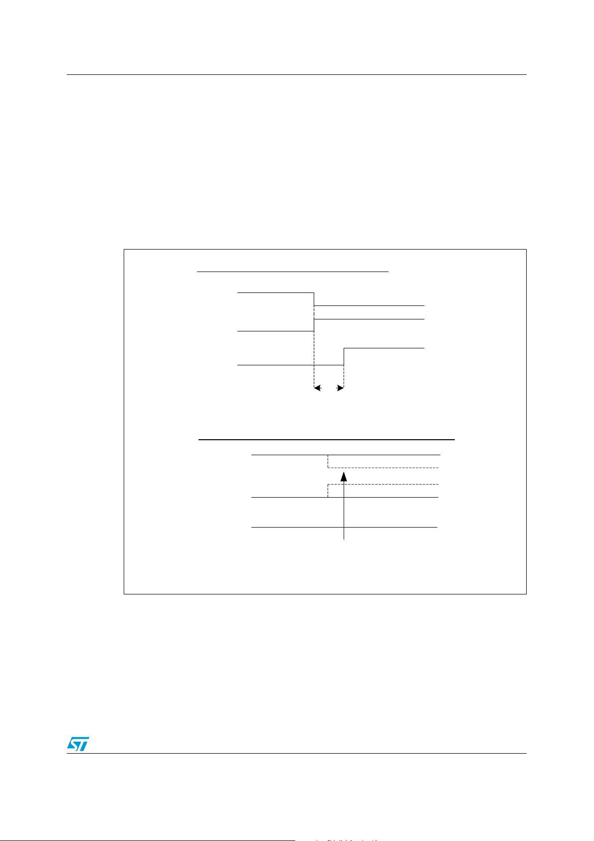
Figure 5. Power-up condition
1a) Power-up condition (normal behavior )
VCC to STLED325I
Internal POR
1b) Power-up condition (processor not responding)
VCC to STLED325I
Internal POR
STBY
READY
MUTE
Guard timer counts up to 10s
STBY
READY
MUTE
READY asserts within 10s which is the desired
behavior, processor is active and not hung
Count over
Guard timer counts up to 10s
READY continues to remain low/high
Due to abnormality in the processor, READY did not
change state from low to high, leading to STBY
assertion
Note: 1 Guard timer is turned off by default upon READY assertion.
2 If Guard timer is to be kept on during READY high condition, the guard timer registers must
be set accordingly by proper commands through I
2
C bus.
3 In this power-up condition, Guard timer is triggered by internal POR pulse.
4 During power-up, the Guard timer value is 10s.
16/62 Doc ID 17576 Rev 1
!-6
STLED325 Functional description
3.10.2 Entering standby mode
The STLED325 controls the power to the main board using the STBY pin. During normal
operation, the STBY pin is a low level which externally controls a Power MOS switch to
enable power to the main board. The STLED325 asserts the STBY pin to a high when any
one of the following conditions occur:
– Processor fails to respond by enabling the READY pin within 10s upon first power-up
(cold boot up)
– Guard timer counts down to 0s
– Processor makes the READY pin to low (can happen in various conditions such as
user presses STBY key on front panel, STBY key on remote control, etc).
Figure 6. Power down condition (normal behavior)
2a) Power-down condition (normal behavior )
READY
MUTE
STBY
2 us
Guard timer is not required here
2b) Power-down condition (abnormal behavior of processor)
READY
MUTE
STBY
In this case the READY remains high and as long as
READY is high, the MUTE is low and STBY is low.
READY continues to remain high
!-6
– Guard timer can be kept on during normal condition when READY is high (depending
on the user).
– In this condition, the guard timer can be disabled or enabled. If the guard timer is
enabled, the timer needs to be cleared before the programmed count of the timer is
reached. If the programmed count is reached, the STBY will be asserted.
– It is advisable not to enable the guard timer during normal operation.
Doc ID 17576 Rev 1 17/62

Functional description STLED325
3.10.3 Wake-up
The STLED325 can wake-up from any one of the following sources:
– Front-panel keys
– Remote-control keys
– Real time clock (RTC) in 3 conditions (alarm, watchdog timer, oscillator fail)
– External wake-up pin (by a low to high transition on this pin)
– GPIO status changes
– READY pin goes from low to high
Figure 7. Standby condition (normal behavior)
3a) Standby condition (normal behavior)
or Key pad or RTC or WAKE_UP for wake up
Hot key command from IR
Guard timer triggers
STBY
READY
MUTE
3b) Standby condition (abnormal behavior, processor is not responding)
Hot key command from IR
or Key pad or RTC or WAKE_UP for wake up
STBY
READY
MUTE
READY asserts within programmed timer value (1s-15s)
Guard timer
triggers
Signals STBY after
guard timer count is over
READY continues to remain low
!-6
– When the hot-key is detected either from front-panel or remote control or RTC or from
a transition (low to high transition) on WAKE_UP pin during stand-by, the STBY pin
de-asserts.
– The de-assertion of the STBY triggers the guard timer.
– The timer value is the programmed value by the user (1-15s). If the user did not
change the value before entering standby, then it remains 10s.
– Also note that the guard timer is off when the STLED325 is in the standby mode.
The guard timer is thus triggered by a de-assertion of the STBY signal or by internal power
on reset signal.
18/62 Doc ID 17576 Rev 1

STLED325 Functional description
3.11 Real time clock (RTC)
The STLED325 integrates a low power Serial RTC with a built-in 32.768 kHz oscillator
(external crystal controlled). Eight bytes of the SRAM are used for the clock/calendar
function and are configured in binary coded decimal (BCD) format. An additional 12 bytes of
SRAM provide status/ control of alarm and watchdog functions. Addresses and data are
transferred serially via a two line, bi-directional I
incremented automatically after each WRITE or READ data byte. Note that all 4 digits must
be enabled before using the RTC display.
Functions available to the user include a non-volatile, time-of-day clock/calendar, alarm
interrupts and watchdog timer. The eight clock address locations contain the century, year,
month, date, day, hour, minute, second and tenths/hundredths of a second in 24 hour BCD
format. Corrections for 28, 29 (leap year - valid until year 2100), 30 and 31 day months are
made automatically.
The RTC operates as a slave device through the slave address of the STLED325 on the
serial bus. Access is obtained by implementing a start condition followed by the correct
device slave address. The 16 bytes contained in the device can then be accessed
sequentially in the following order:
–1. Reserved
– 2. Seconds register
– 3. Minutes register
– 4. Hours register
– 5. Day register
– 6. Date register
– 7. Century/month register
– 8. Year register
– 9. Calibration register
– 10. Watchdog register
– 11 - 16. Alarm registers
2
C interface. The built-in address register is
The RTC keeps track of the date and time. Once the date and time are set, the clock works
when the STLED325 is in normal operation and standby operation. Wake-up alarm feature
is also included in the RTC module. The accuracy of the RTC is approximately 20 ppm
(±50secs/month). How-ever this much depends on the accuracy of the external crystal
used.
The wake-up alarm is programmed to wake up once the date and time set are met. This
feature is present in normal and standby mode of operation. Only one date and time is
available for setting.
The real time clock (RTC) uses an external 32.768 kHz quartz crystal to maintain an
accurate internal representation of the second, minute, hour, day, date, month, and year.
The RTC has leap-year correction. The clock also corrects for months having fewer than 31
days.
3.11.1 Reading the real time clock
The RTC is read by initiating a Read command and specifying the address corresponding to
the register of the real time clock. The RTC registers can then be read in a sequential read
mode. Alarms occurring during a read are unaffected by the read operation.
Doc ID 17576 Rev 1 19/62
Functional description STLED325
3.11.2 Writing to the real time clock
The time and date may be set by writing to the RTC registers. The new RTC time can be
updated by writing to the RTC registers. The new time only takes affect after a complete
write cycle. If the write cycle is incomplete, the new time value is discarded. A single byte
may be written to the RTC without affecting the other bytes.
3.11.3 Register table for RTC
Table 2. Register table for RTC
Addr D7 D6 D5 D4 D3 D2 D1 D0 Functional/range BCD format
00h Reserved Reserved
OSC_S
01h
02h Rsvd 10 minutes Minutes Minutes 00-59
03h MD_HM_MS 10 hours Hours (24 hours format) Hours 00-23
04h Rsvd Rsvd Rsvd Rsvd Rsvd Day of week Day 01-7
05h Rsvd Rsvd 10 date Day of month Date 01-31
06h CB1 CB0 Rsvd 10M Month Century/month 0-3/01-12
T
10 seconds Seconds Seconds 00-59
07h 10 years Year Year 00-99
08h 12/24 Rsvd
09h RB2 BMB4 BMB3 BMB2 BMB1 BMB0 RB1 RB0 Watchdog
0Ah AFE Rsvd ABE AI 10M Alarm month Al month 01-12
0Bh RPT4 RPT5 AI 10 date Alarm date Al date 01-31
0Ch RPT3 RPT6 AI 10 hour AIarm hour AI hour 00-23
0Dh RPT2 Alarm 10 minutes Alarm minutes Al min 00-59
0Eh RPT1 Alarm 10 seconds Alarm seconds Al sec 00-59
0Fh WDFEn Alarm: day of week Rsvd (bypass mode) Flags
Cal_sig
n
Calibration Calibration
Legend:
Cal_Sign = Sign bit
OSC_ST = Oscillator Stop bit
BMB0 – BMB4 = watchdog multiplier bits
CB = Century bits
ABE = Alarm in battery back up mode enable bit
AFE = Alarm flag enable
RB0 – RB2 = watchdog resolution bits
RPT1 – RPT6 = alarm repeat mode bits
20/62 Doc ID 17576 Rev 1

STLED325 Functional description
WDFEn = watchdog flag enable
12/24 = 12 hour or 24 hour format (‘0’ for 24-hour format and ‘1’ for 12-hour format). For 12
hour PM display, the 8th segment of last digit (digit 4) is driven to indicate PM mode through
a dot on the last digit.
It is recommended to fill the unused bits in the register map to 0 upon a cold boot up. The
timekeepers and alarm store data in BCD format, while the calibration, watchdog bits are in
binary format.
The structure of the frame is shown below. For RTC, all the Dig1 to Dig4 must be configured
to show the proper time.
Figure 8. Keyscan and digit mapping
Digit 5
Keyscan
(used for
discrete LED)
If the date programmed in the RTC exceeds a valid date value, then the RTC does not
function as desired. So the invalid dates should never be programmed into the RTC.
3.11.4 Setting alarm clock registers
Address locations 0Ah-0Eh contain the alarm settings. The alarm can be configured to go
off at a prescribed time on a specific month, date, hour, minute, or second or repeat every
year, month, day, hour, minute, or second. It can also be programmed to go off while the
STLED325 is in the standby mode to serve as a system wake-up call.
Bits RPT6-RPT1 put the alarm in the repeat mode of operation. Codes not listed in the table
default to the once per second mode to quickly alert the user of an incorrect alarm setting.
Note that by default, the alarm repeat mode is enabled and by default the repeat frequency
is set to “once per year”.
Dig 1 Dig 2
Dig 3
Dig 4
AM08722V1
Address locations 0Ah to 0Eh contain the alarm settings. The alarm can be configured to go
off at a prescribed time. The default repeat alarm mode is once per year. Programming the
RPT[6:1] bits changes the repeat alarm mode.
Doc ID 17576 Rev 1 21/62

Functional description STLED325
Table 3. Alarm repeat modes
RPT5 RPT4 RPT3 RPT2 RPT1 RPT6 Repeat alarm mode
1 1 1 1 1 1 Once per week
1 1 1 1 1 0 Once per second
1 1 1 1 0 0 Once per minute
1 1 1 0 0 0 Once per hour
1 1 0 0 0 0 Once per day
1 0 0 0 0 0 Once per month
00 0 0 0 0Once per year
If the RPT value is other than the valid ones listed in the table, the default repeat alarm
mode is once per second so as to quickly alert the user of an incorrect alarm setting.
When the clock information matches the alarm clock settings based on the match criteria
defined by RPT[6:1], then the alarm flag is set. Then if the alarm flag enable bit, is also set,
this will activate the alarm interrupt. Interrupt is cleared by reading the Interrupt registers.
3.11.5 Century bits
The clock shall include correction for leap years. The clock shall also correct for months
fewer than 31 days. Corrections for 28, 29 (leap year –valid until year 2100), 30, 31 day
months must be made automatically.
The two Century bits increment in a binary fashion at the turn of the century, and handles all
leap years correctly. See table for additional explanation.
Table 4. Century bits examples
CB[0] CB[1] Leap year? Example
00Yes2000
0 1 No 2100
1 0 No 2200
1 1 No 2300
1. Leap year occurs every 4 years (for years evenly divisible by 4), except for years evenly divisible by 100.
The only exceptions are those years evenly divisible by 400. (The year 2000 was a leap year, year 2100 is
not.)
(1)
22/62 Doc ID 17576 Rev 1

STLED325 Functional description
3.11.6 Initial power-on defaults
Upon application of power to the device, the register bits in the RTC initially power-on in the
state indicated in table below.
Table 5. Initial power-on defaults
OSC_ST AFE WDFEn
000
Initial power-on defaults value of the RTC registers.
Note: All other control bits power-up in a default state of 0 unless otherwise specified.
Doc ID 17576 Rev 1 23/62

Functional description STLED325
3.11.7 Programmable display
The default display of the RTC time is the 2 MSB digit for hour and the 2 LSB digit for
minutes. However, if the MD_HM_MS bit is set, then the RTC display for the digits can be
changed according to Ta bl e 6 .
Table 6. RTC display
MD_HM_MS RTC display
10 Date-month
00 Hour-minute (default and recommended)
01 Minute-second
11 Month-date
3.11.8 Lookup table with ppm against the calibration register values
The lookup table of the calibration register values for the equivalent ppm is shown in Tab l e 7
below:
Table 7. LUT with ppm against the calibration register values
Sign bit Counts/bit PPM
0000000
0000012
0000104
0000116
0001008
00010110
00011012
00011114
00100016
00100118
00101020
00101122
00110024
00110126
00111028
00111131
01000033
01000135
01001037
01001139
01000041
01000143
01001045
01001147
24/62 Doc ID 17576 Rev 1

STLED325 Functional description
Table 7. LUT with ppm against the calibration register values (continued)
Sign bit Counts/bit PPM
01110049
01110151
01111053
01111155
01110057
01110159
01111061
01111163
1000000
100001-4
100010-8
100011-12
100100-16
100101-20
100110-24
100111-28
101000-33
101001-37
101010-41
101011-45
101100-49
101101-53
101110-57
101111-61
110000-65
110001-69
110010-73
110011-77
110000-81
110001-85
110010-90
110011-94
111100-98
111101-102
111110-106
111111-110
111100-114
111101-118
111110-122
111111-126
Doc ID 17576 Rev 1 25/62

Functional description STLED325
3.12 Remote control decoder
The remote control (RC) decoder module decodes the signal coming from IR_IN pin. The IR
remote control protocols recognized by STLED325 are Philips-RC-5, RCMM, Thomson
RCA, R2000, NEC and R-STEP protocols. The selection of remote control protocol to use is
done by setting the RC protocols register. The command from the remote control is used to
wake-up from standby and resume normal operation. All RC keys can be programmed to act
like RC hotkeys. Upon receiving any one of the designated hotkeys, wake-up operation
begins.
The address of the appliance (8-bit) is stored first into the internal RAM. Then, the command
for the hotkeys is programmed into the internal RAM. Each hotkey memory address could
accommodate one byte (8-bit). Usually one byte is reserved for one command. The hot-keys
can be configured to wake-up the system by more than one RC device address (up to a
maximum of 8 device addresses).
3.13 Interrupt
The STLED325 interrupts the Host by pulling the IRQ_N pin to a low-level both in normal
mode of operation and during wake-up. The interrupt is enabled by STLED325 when any of
the conditions occur:
– Front panel key press in normal operation or during system standby state
– Remote control key press in normal operation or during system standby state
(including the toggle bit changes for all RC protocols)
– A low-to-high on the external pin, WAKE_UP
– Real time clock triggers (alarm, watchdog timer, 32 kHz oscillator fails)
– GPIO input changes
– Low battery indication
– Thermal shutdown
The IRQ_N is an active low level signal and is cleared only after the Interrupt buffer is read.
After reading the interrupt buffer, the Host will know the actual source of the interrupt. This
allows the Host to exactly know the event which caused the interrupt (e.g STBY key on the
Front Panel). The interrupt signal is used to inform the Host of any events detected by the
STLED325. Note that the IRQ_N pin is an open-drain pin which requires an external pull-up
resistor.
Figure 9. Interrupt
The interrupt output is of active low level type.
26/62 Doc ID 17576 Rev 1

STLED325 Functional description
While the interrupt is being read by the MCU and a new GPIO or key data comes in, no new
interrupt is generated but the register for GPIO and KEY data is updated so that the MCU
does not miss the new KEY and GPIO data.
3.14 Ready
The STLED325 supports cutting-off power to the main board for standby operation for good
power management. STBY will be set to high when the READY transitions from high to low.
During a cold boot up or wake up from standby, if the READY pin stays low, the STLED325
will assert the STBY when the guard timer has finished counting down to 0.
When the READY drops to a low, MUTE goes high immediately and soon after (2µs
minimum) the STBY is asserted.
In the normal mode of operation, when READY is a high, the STBY is asserted only when
the guard timer is enabled and has finished counting down to 0. This is meant to put the
system into stand-by as the READY pin was stuck at high and the guard timer register was
not cleared before it finished counting down to 0. It is advised to disable the guard timer
during normal operation.
3.15 Mute
The MUTE pin will be set to logic high to mute the audio output before power is cut to the
host processor. In wake up mode, the MUTE pin will be set to logic low to enable the audio
output immediately after the high assertion of the READY pin. In general, MUTE follows
READY pin with an inverted polarity. This pin is used to prevent pop-up sound during powerup and power-down states.
3.16 GPIO
The STLED325 supports 2 additional GPIOs that can be configured as inputs or outputs. As
an input, the GPIO can be used to interface to a sensor or a switch or key and as an output,
the GPIO can be used to drive individual indicator LEDs.
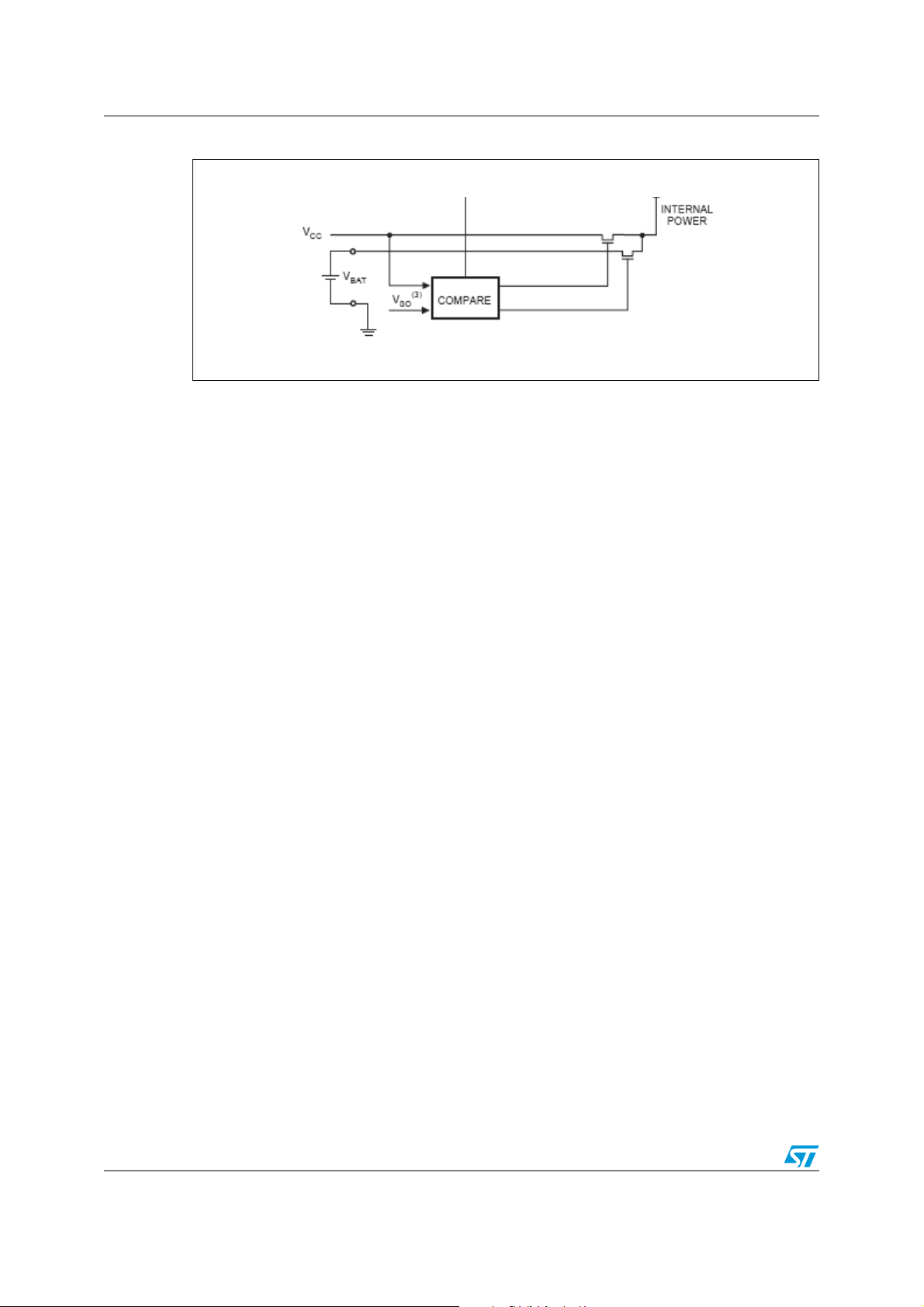
3.17 Power sense circuits
The STLED325 has a built-in power sense circuit which detects power failures and
automatically switches to the battery or super-cap supply when a power failure occurs. The
energy needed to sustain the SRAM and clock operations can be supplied by small lithium
button supply or a super-cap when a power failure occurs. When operating from the battery
or super-cap, all the inputs and outputs are driven to a known state (generally L).
Doc ID 17576 Rev 1 27/62
Functional description STLED325
Figure 10. Power sense circuit
For the STLED325 itself, there is the normal operational mode where the supply is from the
5V V
from the V
To conserve power and maintain long battery life in this battery supply mode, only the RTC
and the clock to the RTC remain operational.
1. The system will only go into battery mode while:
. When the VCC drops below a pre-defined low level, the supply source is switched
CC
to the battery or super-cap supply.
CC
Vcc < 3.5 V and Vcc < Vbat.
So, it means that the system will only switch to battery mode when Vcc drop below 3.5V and
Battery voltage is higher V
voltage.
CC
2. The system will enter back into Vcc mode from battery mode while:
V
> V
CC
bat
It means that the system will switch back to Vcc mode as soon as the VCC is higher than
Vbat.
The STLED325 continually monitors Vcc for an out-of-tolerance condition. Should V
below the Switchover voltage (V
= 3.5 V), the device goes into a low-power mode. Inputs
SO
CC
fall
to the device will not be recognized at this time to prevent any erroneous data or outcome
from device. The device also automatically switches over to the battery and powers down
into an ultra low current mode of operation to maximize the super-cap or battery duration. As
system power returns and V
and the power supply is switched to the external V
rises above Vbat, the battery or super-cap is disconnected
CC
. During the battery or super-cap back-
CC
up mode, the clock registers of RTC are maintained by the attached battery or super-cap.
On power-up, when V
returns to a nominal value, write protection continues for t
CC
REC
(refer
to timing diagram in later part of spec).
Upon power-up, the device switches from battery to V
when VCC > Vbat. When VCC rises
CC
above Vbat, it will recognize the inputs.
28/62 Doc ID 17576 Rev 1

STLED325 Functional description
Figure 11. Circuit
The minimum operating voltage of STLED325 is 2.5 V with a typical VBAT voltage of VCCVF (diode). Therefore, the typical delta voltage swing across the capacitor is
ΔV = V
– VF – V
CC
where VF is approximately 0.5 V. Therefore,
ΔV = 5 – 0.5 – 2.5 = 2 V
Since the typical battery current (IBAT) is limited to 7 µA, the capacitance and duration of
power-out time can be calculated using the formula:
I = CΔV/Δt
Where I = 7µA, ΔV=2V, C= capacitance in Farads and Δt is power-out time in seconds.
Using a 0.1F super-cap, for example, the equation would be:
7µA = 0.1F x 2V/Δt
Solving for Δt, the typical power-down time is about 28,571 seconds = 8 hours.
3.17.1 Switchover
During the period the VCC falls, in order for the battery switchover circuit to work reliably, the
fall time of V
trigger and switch from V
period from 0V to 5V, the rise time of V
Figure 12. Battery switchover waveform
from 5V to 0V should be at least 100µs. This is to allow the comparator to
CC
CCmin
CC
to V
mode should there be a need. During the VCC rise
BAT
is not critical. This is indicated by the Figure 12.
CC
Also note that for battery operation, there will be a current spike of 5mA in 10us into the
battery when V
CC
to V
switchover happens. From V
BAT
Doc ID 17576 Rev 1 29/62
to VCC switching, the current
BAT

Functional description STLED325
spike is very low into the battery. The battery must be protected against such spikes. This is
not relevant for super-cap.
During the switching from V
to VCC, the I2C is active after a minimum of 5ms.
BAT
3.17.2 Battery low warning
The STLED325 automatically performs battery voltage monitoring upon power-up. If the
interrupt for this condition (ABE) is enabled, the RTC will generate an interrupt pulse if the
battery voltage is found to be less than a minimum of 2.5V. However, this condition is
unlikely to go away very quickly as time is needed for the battery to be replaced, and it is not
desirable to keep issuing an interrupt.
Therefore when this bit is set, this condition is checked once every week. If the condition is
still true, then interrupt is sent again.
The ABE bit is an enable bit for battery status check. If the ABE bit was set and the battery
low is generated during a power up sequence, this indicates that the battery is below
approximately 2.5 V and may not be able to maintain data integrity. At this point, a fresh
battery needs to be installed or the super-cap recharged.
This situation only occurs when a battery is used but not with a super-cap as the super-cap
re-charges when the supply is present.
3.17.3 Different power operation modes
The device is capable to support the different power modes as shown in the Table 8.
Table 8. Different power operation modes
V
CC
V
BAT
Present Present V
Present Absent (Float or 0V)
V
Absent (Float or 0V) Present V
V
< 3.5V V
CC
Absent (Float or 0V) Absent (Float or 0V)
BAT
> V
CC
V
Condition Operation
Normal operation of
chip from V
Normal operation of
chip from V
CC until VCC
is 3.5V
CC
V
CC
> V
CC
> V
BAT
BAT
> 3.5V
and
Chip operations from
BAT
> 2.5V
V
in a low power
BAT
mode of operation
Chip operations from
V
in a low power
BAT
mode of operation
< 3.5V and
CC
V
< 2.5V
BAT
Chip does not function.
Completely shutdown.
CC
30/62 Doc ID 17576 Rev 1

STLED325 Functional description
3.18 Bus characteristics
The bus is intended for communication between different ICs. It consists of two lines: a bidirectional data signal (SDA) and a clock signal (SCL). Both the SDA and SCL lines must be
connected to a positive supply voltage (typical voltage is 3.3 V) via a pull-up resistor (typical
value is 10 K). The following protocol has been defined.
- Data transfer may be initiated only when the bus is not busy.
- During data transfer, the data line must remain stable whenever the clock line is High.
- Changes in the data line, while the clock line is High, will be interpreted as control
signals.
Accordingly, the following bus conditions have been defined:
Bus not busy: Both data and clock lines remain High.
Start data transfer: A change in the state of the data line, from high to Low, while the clock
is High, defines the START condition.
Stop data transfer: A change in the state of the data line, from Low to High, while the clock
is High, defines the STOP condition.
Data valid: The state of the data line represents valid data when after a start condition, the
data line is stable for the duration of the high period of the clock signal. The data on the line
may be changed during the Low period of the clock signal. There is one clock pulse per bit
of data.
Each data transfer is initiated with a start condition and terminated with a stop condition.
The number of data bytes transferred between the start and stop conditions is not limited.
The information is transmitted byte-wide and each receiver acknowledges with a ninth bit.
By definition a device that gives out a message is called “transmitter,” the receiving device
that gets the message is called “receiver.” The device that controls the message is called
“master.” The devices that are controlled by the master are called “slaves.”
Acknowledge: Each byte of eight bits is followed by one Acknowledge Bit. This
Acknowledge Bit is a low level put on the bus by the receiver whereas the master generates
an extra acknowledge related clock pulse. A slave receiver which is addressed is obliged to
generate an acknowledge after the reception of each byte that has been clocked out of the
master transmitter.
The device that acknowledges has to pull down the SDA line during the acknowledge clock
pulse in such a way that the SDA line is a stable Low during the High period of the
acknowledge related clock pulse. Of course, setup and hold times must be taken into
account. A master receiver must signal an end of data to the slave transmitter by not
generating an acknowledge on the last byte that has been clocked out of the slave. In this
case the transmitter must leave the data line High to enable the master to generate the
STOP condition.
Note: Refer to Philips I
2
C specification or contact STMicroelectronics for more information on I2C.
Doc ID 17576 Rev 1 31/62
Functional description STLED325
Table 9. Pin description
Pin number Symbol Type Name and function
1 MUTE OUT
2IRQ_NOUT
Output from the STLED325 to gracefully mute the audio
before entering standby mode
Interrupt output (active low level type) to interrupt the
MCU under various conditions
3 GPIO0 IN/OUT GPIO0 that can be configured as an input or output
4 GPIO1 IN/OUT GPIO1 that can be configured as an input or output
5 IR_IN IN Remote control data input
2
6 SDA IN/OUT I
7SCLINI
8 WAKE_UP Input
C compatible serial data I/O
2
C compatible serial clock input
Wake-up pin (can be used for wake-up on detecting a low
to high transition). AV wake-up or CEC wake-up.
Digit output pin. Can be used in conjunction with 8
9DIG5OUT
segment outputs to control 8 discrete LEDs on the front
panel.
10 - 13 DIG4 –DIG1 OUT Digit output pins
5.0 V ± 10% main supply voltage. Bypass to GND
14 VCC PWR
through a 0.1 µF capacitor as close to the pin as
possible.
Input data to these pins from external keyboard are
15, 16 KEY2-KEY1 IN
latched at end of the display cycle (maximum keyboard
size is 8 x 2). 5V digital input.
SEG8/KS8
17 - 24
to
OUT Segment output pins (dual function as key source)
SEG1/KS1
Current sense input. Connect resistor to ground to set
25 ISET IN
constant current through LEDs. Connect to GND through
a resistor to set the peak segment current.
26 VBAT Input
Battery power supply for the RTC when there is no
supply to the chip
27 VREG Output 1.8V regulator output. Connect to an external capacitor.
28 GND PWR Connect this pin to system GND
29 XIN IN Connect to an external crystal or apply external clock
30 XOUT OUT Output of the external crystal. Open when external clock
31 STBY OUT Hardware pin to control the power to the Host
32 READY IN
Input to the device from the Host to indicate that Host is
ready
EPAD Exposed pad. Connect to PCB GND.
32/62 Doc ID 17576 Rev 1

STLED325 Electrical ratings
4 Electrical ratings
4.1 Absolute maximum ratings (TA = 25 °C, GND = 0 V)
Absolute maximum ratings are those values above which damage to the device may occur.
Functional operation under these conditions is not implied. Exposure to absolute maximum
rating conditions for extended periods may affect device reliability. All voltages are
referenced to GND.
Table 10. Absolute maximum ratings (T
Symb
ol
V
Supply voltage to ground -0.5 to +7.0 V
CC
Logic input voltage (KEY1, KEY2 inputs) -0.5 to +7.0 V
V
I
V
Logic input voltage (all input pins except KEY1, KEY2) -0.5 to +3.6 V
I
Power dissipation
P
D
Operating ambient temperature -40 to 85 °C
T
A
T
Junction temperature 150 °C
J
T
V
Table 11. Thermal data
Storage temperature -65 to +150 °C
STG
Lead temperature (10 sec) 300 °C
T
L
Electrostatic discharge voltage on all
pins
2
ESD
Parameter Value
1
= 25 °C, GND = 0 V)
A
1200 mW
Human body model -2 to +2 kV
Symbol Parameter QFN 32 Unit
R
Tj-c
Thermal resistance junction-case TBD °C/W
Uni
t
Doc ID 17576 Rev 1 33/62

Electrical ratings STLED325
4.2 Recommended operating conditions
4.2.1 DC electrical characteristics
(TA = -40 to +85 °C, VCC = 5.0 V ± 10%, GND = 0 V)
Table 12. DC electrical characteristics
Symbol Parameter Test conditions Min Typ Max
V
V
REG
V
V
V
V
I
IH
V
HYS
V
I
OLEAK
I
SEG
I
DIG
I
TOLSEG
External supply voltage 4.5 5.0 5.5 V
CC
Internal logic supply voltage and
regulator output
HIGH level input voltage (all digital
IH
pins except KEY1 and KEY2)
LOW level input voltage (all digital
IL
pins except KEY1 and KEY2)
HIGH level input voltage (KEY1 and
IH
KEY2 pins)
LOW level input voltage (KEY1 and
IL
KEY2 pins)
, I
Input current (all pins) VIN = VIH or V
IL
High level
guaranteed
Low level
guaranteed
High level
guaranteed
Low level
guaranteed
1.62 1.8 1.98 V
1.35 1.98 V
00.45V
35.5V
02V
IL
-2 2 µA
Hysteresis voltage (digital pins) 0.2 V
Low level output voltage (Digital
OL
output pins)
= 4 mA 0.4 V
I
OL2
Driver leakage current Drivers off -150 µA
V
= VF = 2.5 V
Segment drive LED sink current
Digit drive LED source current V
Segment drive current matching
LED
= VCC – 1.0
V
DIGIT
= VCC – 1.0 240 320 400 mA
DIGIT
=5.0 V,
V
CC
T
=25°C
A
=2.5V; LED
V
LED
-30 -40 -50 mA
±4.0 %
current = 40 mA
R
SET
External current setting reference
resistor (precision = ±1% tolerance)
I
= 40 mA 360 Ω
SEG
Uni
t
34/62 Doc ID 17576 Rev 1

STLED325 Electrical ratings
4.3 Power consumption estimation
Each port of the STLED325 can sink a maximum current of 40 mA into an LED with a 3.4 V
forward voltage drop when operated from a supply voltage of 5.0 V. The minimum voltage
drop across the internal LED drivers is thus 5.0 - 3.4 = 1.6 V. The STLED325 can sink
8 x 40 = 320 mA when all outputs are operating as LED segment drivers at full current. On a
5.0 V supply, a STLED325 dissipates (5.0 V-3.4 V) x 320 mA = 512 mW when driving 8 of
these 3.4 V forward voltage drop LEDs at full current. If the application requires high drive
current, consider adding a series resistor to each LED to drop excessive drive voltage offchip.
If the forward voltage of the LED is lesser than 4.4 V (say 2.4 V), then the maximum power
dissipation of STLED325 when all segments are turned on will be (5 - 2.4) V x 320 mA =
832 mW. To lower the power dissipation, consider adding a small series resistor in the
supply. Another alternative is to in-crease the value of the RSET to lower the current of the
LEDs from 40 mA to say 30 or 20 mA.
The efficiency will be the power consumption in the LEDs divided by the input power
consumed.
Equation 1 Efficiency = Vdiode x Idiode / V
CC
x I
CC
As an example, consider LED with forward voltage of VF = 2.4 V, Ipeak = 40 mA, VCC (max)
= 5.5 V, N=number of segments=8(max), D=duty cycle=15/16,
Power dissipation, PD (max) = 5 mA x 5.5 V + (5.5-2.4) V x (15/16) x 40 mA x 8 = 27.5 + 780
= 807.5 mW. To lower this value, add a series resistor with the supply.
Table 13. Voltage drop estimation with RGB LED
Typica l forwa rd
LED
Red 2.2 V 40 mA 5 V 1 V 2.2 V 1.8
Green 2.5 V 40 mA 5 V 1 V 2.5 V 1.5
Blue 3V 40mA 5V 1V 3V 1V
voltage
VF
Typica l
current
Typical supply
voltage
Digit driver
drop
External
VF
Segment
driver
drop
Note that the above analysis is for a typical condition. If the VF is higher and the supply
voltage is lower than 5V, then it is recommended to operate the LED at a lower current than
40mA in order to have enough headroom for the digit and segment drivers so as not to affect
the brightness and matching.
Table 14. Capacitance (TA = 25°C, f = 1 MHz)
Symbol Parameter Test conditions Min Typ Max Unit
C
IN
Input capacitance
(all digital pins)
Doc ID 17576 Rev 1 35/62
15 pF
Electrical ratings STLED325
Table 15. Power supply characteristics (T
= -40 to 85°C)
A
Symbol Parameter Test conditions Min Typ Max Unit
All blocks of chip ON except
that no display load
= 5.5V
V
CC
Display OFF
= 5.5V
V
CC
TBD mA
2mA
I
CC
I
CC(Q)
Operating power supply
current
Quiescent supply current
)
Table 16. Dynamic switching characteristics (TA = -40 to +85 °C, VCC = 5.0V ± 10%,
GND=0.0V, Typical values are at 25°C)
Symbol Parameter Min Typ Max Units
f
SCL
t
LOW
t
HIGH
t
R
t
F
tHD:STA
tSU:STA
tSU:DAT Data setup time* 100 ns
SCL clock frequency 0 400 kHz
Clock low period 1.3 µs
Clock high period 600 ns
SDA and SCL rise time 300 ns
SDA and SCL fall time 300 ns
START condition hold time
(after this period the first clock pulse is
600 ns
generated)
START condition setup time
(only relevant for a repeated start condition)
600 ns
tHD:DAT Data hold time 0 µs
tSU:STO STOP condition setup time 600 ns
tBUF
Time the bus must be free before a new
transmission can start
1.3 µs
trec Watchdog output pulse width 96 98 ms
Note: The transmitter must internally provide a hold time to bridge the undefined region (300ns
max) of the falling edge of the SCL.
36/62 Doc ID 17576 Rev 1

STLED325 Electrical ratings
Table 17. Timing characteristics (T
= -40 to +85 °C, VCC = 5.0 V ± 10%, GND=0.0 V,
A
typical values are at 25 °C)
Parameter Symbol Min Typ Max Unit Test conditions
Propagation delay
time
t
t
t
TZH1
Rise time
t
TZH2
Fall t ime t
Input capacitance C
Mute active to
standby active
GPIO edge to
interrupt trigger
TM-S 2µs
T
PLZ
PZL
THZ
irq
I
8µs
300 ns
100 ns
2µs
0.5 µs
CLK -> SDA
= 15 pF, RL = 10 kΩ
C
L
Seg1 to Seg12
CL =
300
pF
Grid1 to Grid8,
Seg13/Grid16 to
Seg20/Grid9
120 µs CL = 300 pF, Segn, Dign
15 pF
Doc ID 17576 Rev 1 37/62

Electrical ratings STLED325
4.4 Oscillator and crystal characteristics
Table 18. Oscillator characteristics
Symbol Parameter Conditions Min Typ Max Unit
V
STA
tSTA Oscillator start time V
CL1 X
CL2 X
1. Reference value. TA = 25 deg C, VCC = 3.0 V, CFM-145 (CL = 6 pF, 32.768 KHz) manufactured by Citizen.
Oscillator start voltage ≤ 10 seconds 1.5 V
= 3.0 V 1 s
CC
IN
OUT
IC-to-IC frequency
variation
(1)
-20 +20 Ppm
25 pF
25 pF
Table 19. Crystal electrical characteristics
Symbol Parameter Conditions Min Typ Max Unit
fo
Rs Series resistance
CL Load capacitance 12.5 pF
1. Externally supplied. ST recommends the Citizen CFS-145 (1.5 x 5 mm) and the KDS DT-38 (3 x 8 mm) for
thru-hole, or the KDS DMX-26S(3.2x8mm) for surface-mount, tuning fork-type quartz crystals. KDS can be
contacted at kouhou@kdsj.co.jp or http://www.kdsj.co.jp. Citizen can be contacted at csd@citizenamerical.com or http://www.citizencrystal.com
2. Circuit board layout considerations for the 32.768KHz crystal of minimum trace lengths and isolation from
RF generating signals should be taken into account.
Resonant
frequency
(1)
(2)
32.768 KHz
35 40
(3)
kΩ
Note: 1 Oscillator is not production tested.
2 Externally supplied. ST recommends the Citizen CFS-145 (1.5 x 5 mm) and the KDS DT-38
(3 x 8 mm) for thru-hole, or the KDS DMX-26S(3.2x8mm) for surface-mount, tuning forktype quartz crystals. KDS can be contacted at kouhou@kdsj.co.jp or http://www.kdsj.co.jp
Citizen can be contacted at csd@citizen-americal.com or http://www.citizencrystal.com
3 Circuit board layout considerations for the 32.768KHz crystal of minimum trace lengths and
isolation from RF generating signals should be taken into account.
4 Guaranteed by design.
38/62 Doc ID 17576 Rev 1

STLED325 Electrical ratings
4.5 ESD performance
Table 20. ESD performance
Symbol Parameter Test conditions Min Typ Max Unit
ESD
MIL STD 883 method 3015
(all pins)
HBM ±2kV
Table 21. Battery range and battery detect
Symbol Parameter Conditions Min Typ Max Unit
VBAT
(1)
Battery supply voltage 2.5 3 3.5
(2)
V
TA=25C,
I
BAT
1. STMicroelectronics recommends the RAYOVAC BR1225 or BR1632 (or equivalent) as the battery supply.
2. For rechargeable back-up, V
Battery supply current
(max) may be considered VCC.
BAT
VCC= 0 V, Oscillator
BAT
=3 V
ON, V
710 uA
Figure 13. Power down/up mode ac waveforms
Table 22. Power down/up AC characteristics
Symbol Parameter
tpD SCL and SDA at V
trec SCL and SDA at V
1. VCC fall time should not exceed 5mV/µs.
2. Valid for ambient operating temperature: T
Table 23. Power down/up trip points DC characteristics
Symbol Parameter
V
SO
V
SO
Battery back-up switchover voltage
(from VCC to V
Battery back-up switchover voltage
BAT
to VCC)
(from V
Doc ID 17576 Rev 1 39/62
(1)(2)
before power down 0 ns
IH
after power-up 10 µs
IH
(1)(2)
=-40 to 85, V
A
= 2.5V to 5.5V (except where noted)
CC
Min Typ Max Unit
Min Typ Max Unit
V
)
BAT
V
V
CC
CC
CC
< 3.5V
and
< V
> V
BAT
BAT
V
V

Electrical ratings STLED325
1. All voltages are referenced to GND.
2. Valid for ambient operating temperature: T
=-40 to 85, V
A
= 2.5V to 5.5V (except where noted)
CC
Table 24. Thermal shutdown characteristics
(1)
Symbol Parameter Conditions Min Typ Max Unit
TSD
Thermal shutdown
threshold
VCC=5V 140 Deg C
THYS Hysteresis VCC=5V 15 Deg C
1. Thermal shutdown is not production tested.
Figure 14. V
characteristics
CC
40/62 Doc ID 17576 Rev 1
STLED325 Display RAM address and display mode
5 Display RAM address and display mode
The display RAM stores the data transmitted from an external device to the STLED325
through the serial interface. The addresses are as follows, in 8-bits unit:
Table 25. Bit map for segment 1 to segment 8
Seg1 Seg4 Seg8
10 H
11 H
12 H
13 H
14 H
L
L
L
L
L
10 H
11 H
12 H
13 H
14 H
U
U
U
U
U
Dig1
Dig2
Dig3
Dig4
Dig5
b0 b3 b4 b7
XX H
L
“0” in memory means GND on outpu; ‘1” in memory means V
XX H
U
on output.
CC
Doc ID 17576 Rev 1 41/62

KEY matrix and key-input data storage RAM STLED325
6 KEY matrix and key-input data storage RAM
The key matrix is of 8x2 configuration, as shown below:
Figure 15. KEY matrix and key-input data storage RAM
The data of each key are stored as illustrated below, and are read by the appropriate read
command, starting from the least significant bit.
Key 1 Key 2 Key 1 Key 2 Key 1 Key 2 Key 1 Key 2
Seg1 KS1 Seg2 KS2 Seg3 KS3 Seg4 KS4
Seg5 KS5 Seg6 KS6 Seg7 KS7 Seg8 KS8
b0 b1 b2 b3 b4 b5 b6 b7
All the front panel keys can be configured as hot keys using the “configuration mode setting
command”. Alternatively, any number of keys out of 16 keys can be programmed for hot key
functions by using the hot-key setting command.
It is recommended to read the hot key values immediately upon STBY de-assertion. If they
are not read within the guard preset timer value, the hot key data are cleared.
It is recommended to have 10 KΩ pull down resistors on the KEY1 and KEY2 input pins and
the output SEG/KS pins can see a maximum load of 300pF. This load condition is important
for the key dis-charge cycle time.
42/62 Doc ID 17576 Rev 1

STLED325 Commands
7 Commands
A command sets the display mode and status of the LED driver.
The first 1 byte input to the STLED325 through the SDA pin after the slave address is
regarded as a command. If slave address is not transmitted before the commands/data are
transmitted, the commands/data being transmitted are invalid (however, the commands/data
already transmitted remain valid).
7.1 Configuration mode setting command
This command initializes the STLED325 and performs any one of the following functions:
i) Selects the duty factor (1/8 to 1/16 duty factor). When this command is executed, display
is turned off. To resume display, the display ON command must be executed. If the same
mode is selected, nothing is performed.
ii) Selects the remote control protocol to use.
iii) Sets the guard timer. The guard timer is configurable from 1 to 15s or turned off
completely.
iv) Sets the guard timer action to perform when the guard timer counts. Two actions are
allowed: no action or set STBY to high level.
MSB LSB
0 0 b5 b4 b3 b2 b1 b0
Bits b7-b6 = 00 is decoded as a configuration mode setting command. The subsequent bits
are de-coded as follows:
b5: enables wake-up from the external WAKE_UP pin
b4: enable for the display configuration setting change (number of digits)
b3: allows display of RTC (during normal or STBY modes)
b2: enables all RC keys as hot-keys
b1: enables all FPK keys as hot-keys
b0: enables the Guard Timer to issue STBY once the timer expires
Note: When displaying the RTC during normal mode, if the µP is writing data to STLED325 using
2
I
C bus, the RTC display on LED momentarily turns off.
The first byte after the configuration command is in the following format:
MSB LSB
b7 b6 b5 b4 B3 b2 b1 b0
Remote control protocol setting (bits b6-b4)
000: RC Disabled (default)
Doc ID 17576 Rev 1 43/62

Commands STLED325
001: Philips RC-6 (optional only enabled for Philips)
010: Philips RC-5
011: Philips RCMM
100: NEC
101: R-STEP
110: Thomson R2000
111: Thomson RCA
When b7=‘0’, incoming RC data is output on SDA in decoded format where the Device
Address, Start Bit, Toggle Bit and Data Bits are sent. Note that the default location is 0x00
for the first device address. This order of the bits sent is in the same format as the incoming
RC data.
When b7=‘1’, incoming raw data (no header information) is output on SDA.
Address decoding is still performed to decode the corresponding RC protocol. The format of
the data on SDA corresponds to the format of the respective RC frame.
For details, refer to the RC protocol section of the datasheet.
GUARD TIMER SETTING (bits b3-b0)
0000: Turned off (guard timer disabled)
0001: 1 seconds
0010: 2 seconds
1111: 15 seconds
The second byte after the configuration command is in the following format:
MSB LSB
b7 b6 b5 b4 b3 b2 b1 b0
7-Segment display mode setting (bits b1-b0)
00: 1 digit, 8 segments (Digit 1 pin output is enabled)
01: 2 digits, 8 segments (Digit 1 and Digit 2 pin outputs are enabled)
10: 3 digits, 8 segments (Digit 1, Digit 2 and Digit 3 outputs are enabled)
11: 4 digits, 8 segments (Digit 1, Digit 2, Digit 3 and Digit 4 outputs are enabled)
b2: configuration for the digital outputs of the chip
b2 = 1 will enable the outputs of the chip to be push pull type to 1.8V
b2 = 0 will enable the outputs of the chip to be open-drain (can be externally pulled up to
3.3V)
b3: configuration for the GPIO0
44/62 Doc ID 17576 Rev 1

STLED325 Commands
b3 = 0 enables the GPIO0 as input
b3 = 1 enables the GPIO0 as output
b4: configuration for the GPIO1
b4 = 0 enables the GPIO1 as input
b4 = 1 enables the GPIO1 as output
b5 = interrupt enable register bit for GPIO (applies to both GPIO0 and GPIO1)
b5 = 0 disables the interrupt generation from any of the two GPIOs
b5 = 1 enables the interrupt generation from any of the two GPIOs inputs change
b6 = configuration of the edge trigger for GPIO0 (works only when b5 is enabled)
b6 = 0 sends interrupt when GPIO0 triggers from a high to a low
b6 = 1 sends interrupt when GPIO0 triggers from a low to a high
b7 = configuration of the edge trigger for GPIO1 (works only when b5 is enabled)
b7 = 0 sends interrupt when GPIO1 triggers from a high to a low
b7 = 1 sends interrupt when GPIO1 triggers from a low to a high
The minimum pulse width for a valid GPIO detection must be 8us minimum.
Upon power application, the following modes are selected:
Display mode setting: the 4-digit, 8-segment mode is selected (default: display off and
keyscan on).
Remote control protocol setting: RC-5.
Guard timer setting: turned on with 10s. After the first command is processed by STLED325,
the guard timer is turned off until it is turned on by the host.
Guard timer action: Issue Standby.
Doc ID 17576 Rev 1 45/62

Commands STLED325
7.2 Data setting command
This command sets the data-write and data-read modes.
MSB LSB
0 1 b5 b4 b3 b2 b1 b0
Description: Bits b7-b6 = 01 is decoded as a data setting command. The subsequent bits are
decoded as follows:
b5 b4 = 00: data write command (see bits b1-b0)
b5 b4 = 01: data write 1 command (see bits b1-b0)
b5 b4 = 10: data read 1 command (see bits b1-b0)
b5 b4 = 11: data read 3 command (see bits b1-b0)
b3: clear the guard timer (no change in guard time)
b2: when set to a 1, the guard timer is forced to enable and starts the count again.
While in normal mode, the count starts
Table 26. Data write command. b5 b4: 00
b1-b0
00
01
Write memory (display or RTC) – Address range: 0x00-0x0F. Start
address pointer location is 0x00.
Write memory (display). Address range: 0x10-0x13. Start ad-dress
pointer location is 0x10.
10 Write memory (discrete LED). Address: 0x14.
11 Write data into GPIOs if they are configured as outputs (see note 1)
Note 1: The following byte with MSB7 and MSB6 corresponds to GPIO[1:0] for data to be
written into GPIO1 and GPIO0 when they are configured as outputs.
Figure 16. Data write command (b7 b6) for GPIO
MSB
MSB7 RSVD
GPIO1
MSB6
GPIO0
RSVD RSVD
LSB
RSVD
RSVD
RSVD
When b7 is 1, it drives logic 1 on GPIO1 output and when it is 0, it drives logic 0 on GPIO1
output.
When b6 is 1, it drives logic 1 on GPIO0 output and when it is 0, it drives logic 0 on GPIO0
output.
46/62 Doc ID 17576 Rev 1

STLED325 Commands
Table 27. Data Write 2 command. B5 b4: 01
B1-b0
00 Reserved
01 Reserved (RC6 disable)
10 Reserved (RC6 enable)
11 Enter standby mode
Any subsequent data bytes in this case will be ignored.
Table 28. Data Read 1 command. b5 b4: 10
b1-b0
00 Read Key (following 2 bytes will contain key data)
Read GPIO register (following 1 byte will contain the GPIO data with
MSB7: GPIO1 data and MSB6: GPIO0 data). This is the input monitor for
01
10
11
GPIO[1:0] for reading purpose. When b7 of subsequent byte is low, it
means that GPIO1 input is low and when it is high, it means that GPIO1
input is high. When b6 of subsequent byte is low, it means that GPIO0
input is low and when it is high, it means that GPIO0 input is high.
Read RC data (following four bytes are the address + command bytes from
RC)
Read Interrupt status register (refer to the Interrupt Flag section for
detailed description)
Table 29. Data Read 2 command. b5 b4: 11
b1-b0
00 Reserved
01 Read configuration byte values (see section on configuration bytes)
10 Read LED display memory
11 Read RTC memory. Address command must be issued prior to reading.
On power application, the normal operation mode and address increment mode is set with
the default display memory address set to 0x10 (start of display memory address location).
Refer to the display memory section.
In the auto increment address mode, the address command is sent once followed by the
data bytes.
Alternatively, the data command can be sent followed by the data bytes. In this case, when
new display data is to be written, the last value of the address will be used and then
incremented. Upon reaching the last display memory address, the address jumps to 0x10,
as it represents the first address location of the display memory.
Doc ID 17576 Rev 1 47/62

Commands STLED325
In fixed address mode, the address command has to be sent followed by the display data.
When next byte of data is to be written, address command has to be sent again before new
display data byte.
When the user wants to read the RTC data from the specified memory location of RTC, the
user must first set the address of the RTC location using “Address Setting Command” after
which send the “Read RTC Register” command.
If the address pointer was located in the display memory location and user issues a “Read
RTC Register” command without sending the “Address Setting Command”, the RTC data is
read from the address location of the previous value of the RTC address pointer.
Thus before reading the RTC register data, the user must set the proper address for RTC
using “Address Setting Command”.
Prior to writing data to the RTC registers, the address of the RTC must be set using the
Address Setting command. Else, if the address pointer happens to be pointing at the LED
display memory, then the data will be written to the address location of the previous value in
the RTC address pointer. This is vice-versa true for the LED display memory.
7.3 Configuration data
Up to a maximum of 5-bytes are sent from LSB to MSB as configuration data. The 29-bytes
represent the following configuration information:
MSB (b7) LSB (b0)
Byte1
B7 B6 B5 B4 B3 B2 B1 B0
Decoded/Raw
RC setting
B7 B6 B5 B4 B3 B2 B1 B0
Interrupt
config for
GPIO1
B7 B6 B5 B4 B3 B2 B1 B0
Interrupt
config for
GPIO0
Not used
RC Protocol setting Guard timer setting
Byte 2
Interrupt
enable config
for GPIOs
GPIO1
configuration
(input or
output)
For display
enable
Front Panel Hot Key Bank 1
Front Panel Hot Key Bank 2
configuration
Byte 3
Byte 4
Byte 5
GPIO0
(input or
output)
Digit 5 discrete
LED config
For display dimming setting
7-segment LED display
configuration setting
On power application, the normal operation mode and address increment mode is set with
the default display memory address set to 0x10 (start of display memory address location).
Refer to the display memory section.
In the auto increment address mode, the address command is sent once followed by the
data bytes.
Alternatively, the data command can be sent followed by the data bytes. In this case, when
new display data is to be written, the last value of the address will be used and then
48/62 Doc ID 17576 Rev 1

STLED325 Commands
incremented. Upon reaching the last display memory address, the address jumps to 0x10,
as it represents the first address location of the display memory.
In fixed address mode, the address command has to be sent followed by the display data.
When next byte of data is to be written, address command has to be sent again before new
display data byte.
When the user wants to read the RTC data from the specified memory location of RTC, the
user must first set the address of the RTC location using “Address Setting Command” after
which send the “Read RTC Register” command.
If the address pointer was located in the display memory location and user issues a “Read
RTC Register” command without sending the “Address Setting Command”, the RTC data is
read from the ad-dress location of the previous value of the RTC address pointer.
Thus before reading the RTC register data, the user must set the proper address for RTC
using “Address Setting Command”.
Prior to writing data to the RTC registers, the address of the RTC must be set using the
Address Setting command. Else, if the address pointer happens to be pointing at the LED
display memory, then the data will be written to the address location of the previous value in
the RTC address pointer. This is vice-versa true for the LED display memory.
7.3.1 Interrupt flags
The interrupt is sent on the IRQ_N pin when any one of the event occurs (FP key pressed,
RC key pressed or preset value of RTC/guard timer is triggered or activity on WAKE_UP pin
or GPIO pins). Simultaneously, the interrupt flags are set. The micro-processor can read the
interrupt flags by send-ing the read interrupt flag register command. The following 16-bit
data is read by the processor after sending this command. This enables the microprocessor
to know what caused the interrupt to occur. If the host sees an interrupt issued from first
byte, it is not necessary to read the second byte.
Figure 17. Interrupt bit mapping in Byte 1
Byte 1:
MSB LSB
&0
&0+
2#+
'0)/;=
'0)/;=
HOTKEY
DURING
WAKEUP
20
HOTKEY
DURING
WAKEUP
4HERMAL
SHUTDOWN
"ATTERYLOW
!-6
Doc ID 17576 Rev 1 49/62

Commands STLED325
Figure 18. Interrupt bit mapping in Byte 2
Byte 2:
MSB LSB
2ESERVED
b7-b4 = Normal operation b3-b0=Wake up operation
24#
WATCHDOG
TIMER
24#
ALARM
24#
FAIL
/SCILLATOR
7AKEUP
PIN
,TO(
OR(TO,
7ATCHDOG
TIMER
24#ALARM
24#
FAIL
/SCILLATOR
!-6
In the normal mode of operation, when any FP or RC key is pressed or when
alarm/watchdog is triggered, the STLED325 sets the flags in the above interrupt flag register
and asserts the IRQ_N pin. The data which caused the interrupt to assert remains in the
buffer until it is changed by another key-press. It is up to the micro processor to issue the
read interrupt command to ascertain what caused the interrupt. If the micro processor does
not issue the interrupt within a specific time, the old data is lost and only the latest data is
reflected in the Interrupt Flag register.
In the standby mode of operation, only the hot-key will cause the interrupt flag to be set and
the IRQ_N pin will be asserted. The micro processor should then read the interrupt to know
what caused the wake-up operation before proceeding with the normal data communication
or asserting STBY again if there is no action to be performed. Upon the first read of the hotkey data, the data in the buffer is cleared.
When the b4 of the above interrupt flag is set, then the µP should read the address 0x0F
from the RTC register space to determine if the alarm was triggered. Only after determining
this, the interrupt flag is cleared and the IRQ_N pin de-asserted.
The IRQ_N pin will only be de-asserted once the interrupt flags have been read. The chip
will continue to send the interrupt periodically (approximately every 40us) to the main Host
chip if the oscillator is down signifying to the Host chip that the frequency is out of spec.
7.4 Address setting command
This command sets an address of the display memory or the address of the RTC register
map.
MSB LSB
1 1 x b4b3b2b1b0
The address range from 00h-0Fh represents the RTC register map. For writing data to RTC
registers, initially the address command is sent followed by the RTC data.
10h-14h represents the 7-segment and discrete LED display correspondence. On power
application, the address is set to 10h. In the auto-increment mode, when the address
reached 0x14, the next ad-dress will be 0x10.
50/62 Doc ID 17576 Rev 1

STLED325 Commands
7.5 Display control and hotkey setting command
1 0 b5 b4 b3 b2 b1 b0
Bits b7-b6 = 10 is decoded as a display control and hotkey setting command. The
subsequent bits are decoded as follows:
b5 = 0: sets display control for dimming setting as shown in the table below.
Display control and dimming setting when b5 = 0
b3.b0: sets dimming quantity.
0000: sets pulse width to 1/16.
0001: sets pulse width to 2/16.
0010: sets pulse width to 3/16.
0011: sets pulse width to 4/16.
0100: sets pulse width to 5/16.
0101: sets pulse width to 6/16.
0110: sets pulse width to 7/16.
0111: sets pulse width to 8/16.
1000: sets pulse width to 9/16.
1001: sets pulse width to 10/16 (default and recommended)
1010: sets pulse width to 11/16.
1011: sets pulse width to 12/16.
1100: sets pulse width to 13/16.
1101: sets pulse width to 14/16.
1110: sets pulse width to 15/16.
1111: sets pulse width to 16/16.
Figure 19. Blanking time
b4: Turns on/off display
Doc ID 17576 Rev 1 51/62

Commands STLED325
0: Display off (keyscan continues)
1: Display on
When b5 = 1, the decoding is based on bits b1-b0 as illustrated below:
b1 b0 = 01: IR hot-key configuration of ADR and DATA. After this 3 bytes are sent which are
in the form ADR+DATA to configure the hot-key for a particular device address. A maximum
of 8 hot keys can be configured from a single device address or 4 hot-keys from two device
addresses and so on. If more than 24 bytes in the form of ADR+DATA are sent, then the
pointer moves back to the first ADR+DATA location.
b1 b0 = 10: FP hot-key configuration. Any of the 16 keys can be configured as hot-keys. 2
bytes of key data command are sent following this command to configure the front-panel
hotkeys.
b4, b3 b2: Reserved
b1b0: 00 or 11 are treated as invalid commands and subsequent data bytes are ignored.
Remote control hot keys when b5 = 1
b1 b0: 01
Following 8-bit is sent to indicate the address for RC and subsequent 16-bit indicates the RC
hot key value itself. So a total of 3 bytes are sent for one hot-key configuration. A total of 24
bytes are re-served for RC hot key configuration. Note that the customer code is
programmable for the RC hotkey for both RCMM and R-STEP RC protocol.
Front Panel Hot Keys when b5 = 1
b1 b0: 10
Front panel hot keys can be configured by sending 2 bytes of key data to configure any key
as hot-key from any of the 2 banks. Any number of keys can be configured as hot-keys.
When input key code matches any one of the predefined key codes stored in the internal
RAM, the STLED325 de-asserts the STBY output.
52/62 Doc ID 17576 Rev 1

STLED325 Commands
7.6 Keyscanning and display timing
Figure 20. Keyscanning and display timing
Grid
Outputs
SEG1
SEG2
SEG3
SEGn
DIG1
tDISP=500us
t=1/16 of
tDISP
DIG2 DIG3 -----------
tFRAME=tDISP * (n+1)
DIGn
n = number of digits
Key Scan
DIG1
AM04168V1
The value is fixed by the internal clock from the oscillator.
One cycle of keyscanning consists of one frame, and data of 8x2 matrices are stored in the
RAM.
Note that the keyscan is only at the end of the frame when the display is ON. When the
display is OFF, the keyscan takes place continuously. The grid/digit is turned off during the
keyscan.
Doc ID 17576 Rev 1 53/62

State STLED325
8 State
8.1 Default state upon power-up
Table below shows the default state of the STLED325 upon power-up.
Table 30. Power-up defaults
Serial number Function Default state
1 Display OFF
2 Key-scan ON
3IR Disabled
4 Display mode 8 segment/1 digit
5 Display address
6 RC protocol Disabled
7 Dimming 10/16 duty factor
8 Hot keys (IR and FP) Disabled
9 Guard timer 10s
10H with address increment
mode
8.2 Initial state
On power application, the 10/16-pulse width is set and the display shows the value
configured in the LED display RAM before entering the standby mode. Thus if TUNE is
required to be shown on the LED upon wake-up, then the user must write the corresponding
digit and segments locations in the LED display memory before going into the standby mode
of operation. The value of the display changes only after user configuration.
If the user wishes to display the RTC value during standby, then the user must configure the
STLED325 by sending the appropriate command. If the user does not configure the
STLED325 to display the RTC in standby, the LED shows the same value as was written
previously in the LED display memory location.
Note that all the hot keys are disabled on power-up. Only the hot-keys (FP or RC) can be
detected to wake-up the system from standby condition.
54/62 Doc ID 17576 Rev 1

STLED325 Remote control protocols
9 Remote control protocols
Contact STMicroelectronics for more information on RC protocols or refer to separate
document (TBD).
Doc ID 17576 Rev 1 55/62

Application information STLED325
10 Application information
10.1 Power supply sequencing
Proper power-supply sequencing is advised for all CMOS devices. It is recommended to
always apply V
before applying any signals to the input/output or control pins.
CC
10.2 I
variation with R
SET
The graph of I
Figure 21. Rext versus Iseg curve
variation with R
SET
SET
SET
is shown in Figure 21.
56/62 Doc ID 17576 Rev 1
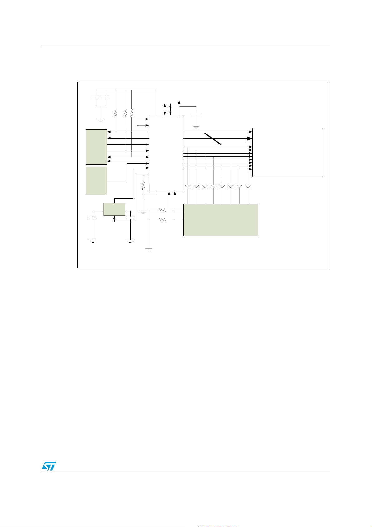
STLED325 Application information
10.3 Application diagram
Figure 22. Application schematic
C1 C2
R3
Crystal
(32.768KHz)
R2
GND
Main CPU
IR re mo te
control
sensor
CL1 CL2
R1
VBAT
WAKE_UP
IRQ _N
STBY
READY
SCL
SDA
MUTE
RSET
IR_ IN
XI
XO
ISET
GND
GND
VCC
GPIO2
GPIO1
DIG5
DIG1-DIG4
STLED325
SEG1/KS1
-SEG 8/KS8
KEY1-KEY2
R4
R5
VREG
Creg
4
D1 D2 D3 D4 D5 D6 D7 D8
Keyscan
(8x2 matrix)
LED 4 -Digit 7-segment
(+dot
-point)
Display panel
With some individual L EDs
AM08725V1
Resistors:
RSET = external resistor for current setting
R1 = 1-10 KO SDA external pull-up resistor
R2 = 1-10 KO SCL external pull-up resistor
R3 = 1-10 KO IRQ_N external pull-up resistor
R4-R5 = 10 KO external key-matrix pull-down resistors
Capacitors:
C1 = 33 µF (25 V) electrolytic
C2 = 0.01-0.1µF (25V) ceramic
Creg=0.1 uF
CL1 = CL2 = 25pF
Diodes
D1-D8 = 1N4148
Supply voltage
V
= 5 V ± 10%
CC
Doc ID 17576 Rev 1 57/62

Package mechanical data STLED325
11 Package mechanical data
In order to meet environmental requirements, ST offers these devices in different grades of
ECOPACK
®
packages, depending on their level of environmental compliance. ECOPACK®
specifications, grade definitions and product status are available at: www.st.com. ECOPACK
is an ST trademark.
Table 31. QFN32 (5 x 5 mm) mechanical data
Millimeters
Symbol
Min Typ Max
A 0.80 0.90 1.00
A1 0 0.02 0.05
A3 0.20
b 0.18 0.25 0.30
D 4.85 5.00 5.15
D2 3.35 3.45 3.55
E 4.85 5.00 5.15
E2 3.35 3.45 3.55
e0.50
L 0.30 0.40 0.50
ddd 0.08
58/62 Doc ID 17576 Rev 1
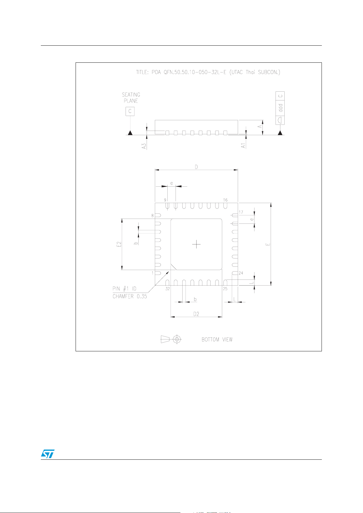
STLED325 Package mechanical data
Figure 23. QFN32 package dimensions
Doc ID 17576 Rev 1 59/62

Package mechanical data STLED325
Figure 24. QFN32 carrier tape
60/62 Doc ID 17576 Rev 1

STLED325 Revision history
12 Revision history
Table 32. Document revision history
Date Revision Changes
27-Apr-2011 1 Initial release.
Doc ID 17576 Rev 1 61/62

STLED325
Please Read Carefully:
Information in this document is provided solely in connection with ST products. STMicroelectronics NV and its subsidiaries (“ST”) reserve the
right to make changes, corrections, modifications or improvements, to this document, and the products and services described herein at any
time, without notice.
All ST products are sold pursuant to ST’s terms and conditions of sale.
Purchasers are solely responsible for the choice, selection and use of the ST products and services described herein, and ST assumes no
liability whatsoever relating to the choice, selection or use of the ST products and services described herein.
No license, express or implied, by estoppel or otherwise, to any intellectual property rights is granted under this document. If any part of this
document refers to any third party products or services it shall not be deemed a license grant by ST for the use of such third party products
or services, or any intellectual property contained therein or considered as a warranty covering the use in any manner whatsoever of such
third party products or services or any intellectual property contained therein.
UNLESS OTHERWISE SET FORTH IN ST’S TERMS AND CONDITIONS OF SALE ST DISCLAIMS ANY EXPRESS OR IMPLIED
WARRANTY WITH RESPECT TO THE USE AND/OR SALE OF ST PRODUCTS INCLUDING WITHOUT LIMITATION IMPLIED
WARRANTIES OF MERCHANTABILITY, FITNESS FOR A PARTICULAR PURPOSE (AND THEIR EQUIVALENTS UNDER THE LAWS
OF ANY JURISDICTION), OR INFRINGEMENT OF ANY PATENT, COPYRIGHT OR OTHER INTELLECTUAL PROPERTY RIGHT.
UNLESS EXPRESSLY APPROVED IN WRITING BY AN AUTHORIZED ST REPRESENTATIVE, ST PRODUCTS ARE NOT
RECOMMENDED, AUTHORIZED OR WARRANTED FOR USE IN MILITARY, AIR CRAFT, SPACE, LIFE SAVING, OR LIFE SUSTAINING
APPLICATIONS, NOR IN PRODUCTS OR SYSTEMS WHERE FAILURE OR MALFUNCTION MAY RESULT IN PERSONAL INJURY,
DEATH, OR SEVERE PROPERTY OR ENVIRONMENTAL DAMAGE. ST PRODUCTS WHICH ARE NOT SPECIFIED AS "AUTOMOTIVE
GRADE" MAY ONLY BE USED IN AUTOMOTIVE APPLICATIONS AT USER’S OWN RISK.
Resale of ST products with provisions different from the statements and/or technical features set forth in this document shall immediately void
any warranty granted by ST for the ST product or service described herein and shall not create or extend in any manner whatsoever, any
liability of ST.
ST and the ST logo are trademarks or registered trademarks of ST in various countries.
Information in this document supersedes and replaces all information previously supplied.
The ST logo is a registered trademark of STMicroelectronics. All other names are the property of their respective owners.
© 2011 STMicroelectronics - All rights reserved
STMicroelectronics group of companies
Australia - Belgium - Brazil - Canada - China - Czech Republic - Finland - France - Germany - Hong Kong - India - Israel - Italy - Japan -
Malaysia - Malta - Morocco - Philippines - Singapore - Spain - Sweden - Switzerland - United Kingdom - United States of America
www.st.com
62/62 Doc ID 17576 Rev 1
 Loading...