

Features
■ Operating input voltage range from 2.3 V to
5.5 V
■ ± 7.5% LED current accuracy
■ Two LEDs in series per channel
■ High side current source
■ Up to 125 mA of total LED current
■ 86% efficiency at 100 mA
■ PWM dimming with automatic shutdown time
window
■ 2.5 MHz switching frequency
■ CSP 12 bumps 0.4 mm. pitch 1.4 x 1.8 mm.
Applications
■ LCD backlight with up to 10 LEDs
■ Cellular phones
■ PDAs
Description
STLED25
5 channels step-up white LED driver
Datasheet − production data
Flip-Chip 12 bumps (1.4 x 1.8 mm.)
continue operating driver channels that are
functioning normally, while avoiding excessive
power consumption or associated thermal issues.
The control technique is able to maintain the
efficiency close to 87% at medium load and
higher than 85% at light or full load. The device
also includes soft-start control, inrush current
limit, thermal shutdown and inductor peak current
limit. The STLED25 is packaged in a 12-bump
CSP (1.4 x 1.8 mm, 0.5 mm height).
The STLED25 is a fixed frequency, high efficiency,
boost DC-DC converter with five parallel high side
current sources. It is capable of providing 125 mA
of total current with a maximum voltage of 7.5 V
on each channel. Each current source supports
single or dual LED connection. The output voltage
of the step-up converter is automatically set at
100 mV above the highest voltage required on
any driver, to guarantee proper operation of the
linear current sources. The device implements a
self-test feature to detect failure of any of the
LEDs and to disable the related channel. The
failure status is reset as soon the IC is disabled.
This mode of failure detection allows the device to
Table 1. Device summary
Order code Package Packaging
STLED25JR Flip-Chip12 Tape and reel
May 2012 Doc ID 022323 Rev 3 1/30
This is information on a product in full production.
www.st.com
30

Contents STLED25
Contents
1 Application schematic . . . . . . . . . . . . . . . . . . . . . . . . . . . . . . . . . . . . . . . 3
2 Pin configuration . . . . . . . . . . . . . . . . . . . . . . . . . . . . . . . . . . . . . . . . . . . . 5
3 Maximum ratings . . . . . . . . . . . . . . . . . . . . . . . . . . . . . . . . . . . . . . . . . . . . 6
4 Electrical characteristics . . . . . . . . . . . . . . . . . . . . . . . . . . . . . . . . . . . . . 7
5 Typical application performance . . . . . . . . . . . . . . . . . . . . . . . . . . . . . . . 9
5.1 Quiescent current consumption . . . . . . . . . . . . . . . . . . . . . . . . . . . . . . . . . 9
5.2 Switching frequency . . . . . . . . . . . . . . . . . . . . . . . . . . . . . . . . . . . . . . . . . . 9
5.3 Continuous output current . . . . . . . . . . . . . . . . . . . . . . . . . . . . . . . . . . . . 10
5.4 Efficiency at 100 mA I
5.5 Efficiency at 75 mA I
5.6 Efficiency at 50 mA I
5.7 Absolute channel accuracy . . . . . . . . . . . . . . . . . . . . . . . . . . . . . . . . . . . 12
5.8 Current matching between LED strings . . . . . . . . . . . . . . . . . . . . . . . . . . 12
5.9 PWM dimming linearity 0.39 - 10% . . . . . . . . . . . . . . . . . . . . . . . . . . . . . 13
5.10 PWM dimming linearity 10 - 100% . . . . . . . . . . . . . . . . . . . . . . . . . . . . . . 13
5.11 Inductor peak current . . . . . . . . . . . . . . . . . . . . . . . . . . . . . . . . . . . . . . . . 14
5.12 Maximum continues output current . . . . . . . . . . . . . . . . . . . . . . . . . . . . . 14
OUT . . . . . . . . . . . . . . . . . . . . . . . . . . . . . . . . . . . . . . . . . . . . . . . 10
OUT . . . . . . . . . . . . . . . . . . . . . . . . . . . . . . . . . . . . . . . . . . . . . . . . 11
OUT . . . . . . . . . . . . . . . . . . . . . . . . . . . . . . . . . . . . . . . . . . . . . . . . 11
6 Detailed description . . . . . . . . . . . . . . . . . . . . . . . . . . . . . . . . . . . . . . . . 16
6.1 Boost DC-DC converter operation . . . . . . . . . . . . . . . . . . . . . . . . . . . . . . 16
6.2 Current setting . . . . . . . . . . . . . . . . . . . . . . . . . . . . . . . . . . . . . . . . . . . . . 16
6.3 EN13 and EN45 . . . . . . . . . . . . . . . . . . . . . . . . . . . . . . . . . . . . . . . . . . . . 16
6.4 Modes of operation . . . . . . . . . . . . . . . . . . . . . . . . . . . . . . . . . . . . . . . . . . 17
6.5 Undervoltage lockout . . . . . . . . . . . . . . . . . . . . . . . . . . . . . . . . . . . . . . . . 17
6.6 Overtemperature protection . . . . . . . . . . . . . . . . . . . . . . . . . . . . . . . . . . . 18
6.7 Open LED protection . . . . . . . . . . . . . . . . . . . . . . . . . . . . . . . . . . . . . . . . 18
6.8 Overvoltage protection . . . . . . . . . . . . . . . . . . . . . . . . . . . . . . . . . . . . . . . 18
6.9 Short LED protection . . . . . . . . . . . . . . . . . . . . . . . . . . . . . . . . . . . . . . . . 18
2/30 Doc ID 022323 Rev 3

STLED25 Contents
7 Application information . . . . . . . . . . . . . . . . . . . . . . . . . . . . . . . . . . . . . 19
7.1 External passive components . . . . . . . . . . . . . . . . . . . . . . . . . . . . . . . . . 19
7.1.1 Inductor selection . . . . . . . . . . . . . . . . . . . . . . . . . . . . . . . . . . . . . . . . . . 19
7.1.2 Input and output capacitor selection . . . . . . . . . . . . . . . . . . . . . . . . . . . 19
7.2 Recommended PCB layout . . . . . . . . . . . . . . . . . . . . . . . . . . . . . . . . . . . 20
8 Package mechanical data . . . . . . . . . . . . . . . . . . . . . . . . . . . . . . . . . . . . 24
9 Revision history . . . . . . . . . . . . . . . . . . . . . . . . . . . . . . . . . . . . . . . . . . . 29
Doc ID 022323 Rev 3 3/30
Application schematic STLED25
1 Application schematic
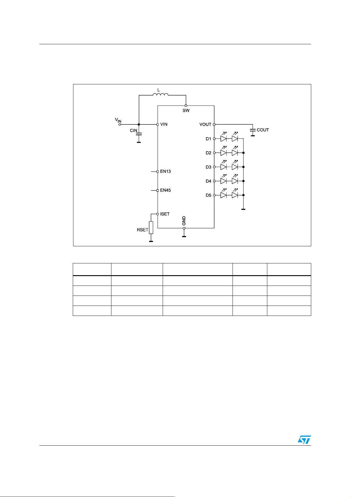
Figure 1. STLED25 application schematic
Table 2. Typical external components
Component Manufacturer Part number Value Size
C
IN
C
OUT
L Samsung CIG21K4R7SCE 4.7 µH 0805
R
SET
1. For 20 mA per branch.
Murata GRM155R60J155M 1.5 µF 0402
Murata GRM219R61A106ME47 10 µF 0805
(1)
25 k
0402
Note: All the above components refer to a typical application. Operation of the device is not limited
to the choice of these external components.
4/30 Doc ID 022323 Rev 3
STLED25 Application schematic
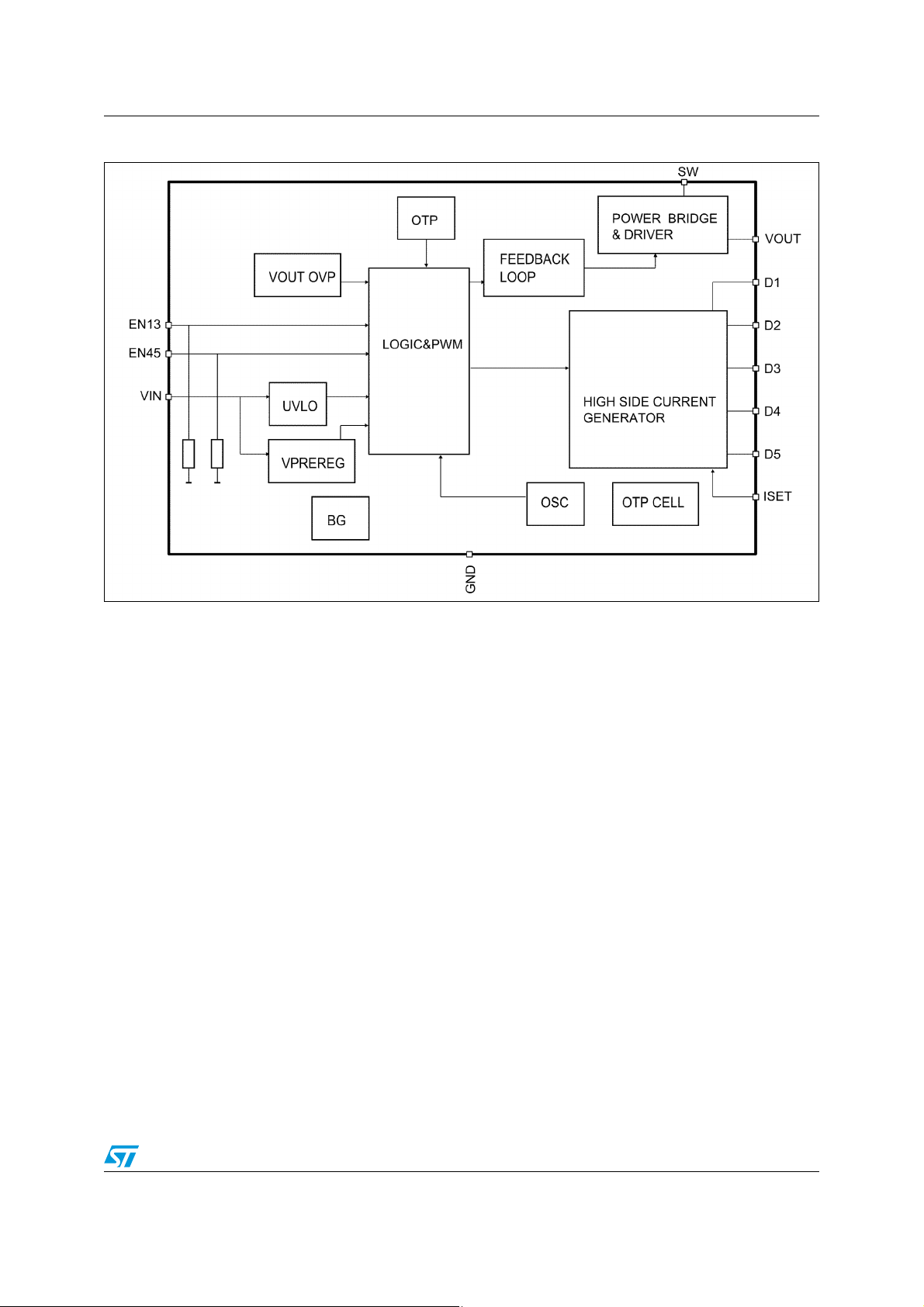
Figure 2. Functional block diagram
Doc ID 022323 Rev 3 5/30

Pin configuration STLED25
2 Pin configuration
Figure 3. Pin configuration (top view)
VIN ISET D1
EN13 EN45 D2
GND D5 D3
SW VOUT D4
AM09921v1
Table 3. Pin description
Pin name Pin number Description
VIN A1 Supply from battery
ISET A2
D1 A3 String 1 controlled by EN13
EN13 B1 Positive polarity. EN13 & 45 Low = IC shutdown
EN45 B2 Positive polarity. EN13 & EN45 Low = IC shutdown
D2 B3 String 2 controlled by EN13
GND C1 Power ground and IC ground
D5 C2 String 5 controlled by EN45
D3 C3 String 3 controlled by EN13
SW D1 Inductor connection to internal switch
VOUT D2 DC-DC output to V
D4 D3 String 4 controlled by EN45
Resistor to GND from 1.28 V (typ.) internal reference: 390x current
multiplier
capacitor
OUT
6/30 Doc ID 022323 Rev 3

STLED25 Maximum ratings
3 Maximum ratings
Table 4. Absolute maximum ratings
Symbol Parameter Value Unit
VIN Supply voltage -0.3 to +6 V
SW Switching node -0.3 to + 11 V
VOUT Output voltage -0.3 to +10 V
D1-D5 LED strings -0.3 to +10 V
EN13, EN45 Signal pins -0.3 to VIN V
ISET Current setting -0.3 V to 2 V
Machine model ± 200
ESD
Charged device model ± 500
VHuman body model ± 2000
T
T
AMB
T
J
STG
Operating ambient temperature -30 to 85 °C
Maximum operating junction temperature +150 °C
Storage temperature -65 to 150 °C
Table 5. Thermal data
Symbol Parameter Value Unit
R
THJA
1. This parameter corresponds to a 4-layer PCB board with 1 inch² of cooling area.
Junction to ambient thermal resistance
(1)
62 °C/W
Doc ID 022323 Rev 3 7/30
Electrical characteristics STLED25
4 Electrical characteristics
- 30 °C < TA < 85 °C, VIN = 3.7 V; V
= 25 °C, unless otherwise specified.
T
A
Table 6. Electrical characteristics
= 7.5 V, EN13 = EN45 = VIN, typical values are at
OUT
Symbol Parameter Test conditions Min. Typ. Max. Unit
General section
V
IN
Operating input voltage 2.3 3.7 5.5 V
Iq Shutdown mode EN13 = EN45 = 0 0.5 2 µA
V
rising 1.9 2.0
V
ν
V
OVP
UVLO
f
SW
I
OUT
I
PK
ν
DC-DC
OVP
HYST
Undervoltage lockout
threshold
Switching frequency 2.25 2.5 2.75 MHz
Continuous output current
Inductor peak current 550 650 mA
OUT
(1)
= 6.2 V;
Application efficiency
(V
= 3.7 V; V
IN
see application schematic)
DC-DC converter efficiency I
Overvoltage protection 8.8 9.05 9.3 V
Overvoltage protection
hysteresis
IN
VIN falling 1.7 1.8
(1)
V
= 2.5 V, V
IN
I
= 50 mA 84
OUT
I
= 75 mA 86
OUT
I
= 100 mA 86
OUT
= 100 mA 88
OUT
= 6.2 V 125 mA
OUT
250 mV
V
%
T
SHDN
Hysteresis 20 °C
LEDs current
Thermal shutdown 150 °C
I
D1-D5
V
SCP
I
LED
I
SET
V
CSH
Current matching -5.5 +5.5 %
Short-circuit protection on
LEDs
Absolute channel accuracy
Voltage reference R
Current mirror I
Measured on the Dx pins 1.28 V
5 mA < I
= 2.5 V to 5.5 V
V
IN
2.5 mA < I
= 2.5 V to 5.5 V
V
IN
SET
/ I
LED
< 25 mA,
LED
< 5 mA,
LED
= 200 k to 15 k 1.28 V
SET
Current source headroom
voltage
8/30 Doc ID 022323 Rev 3
-7.5 +7.5 %
-10 10 %
390 A/A
135 mV

STLED25 Electrical characteristics
Table 6. Electrical characteristics (continued)
Symbol Parameter Test conditions Min. Typ. Max. Unit
I
RIPPLE
PWM
I
LED_LEAK
I
LED_MAX
LED peak-to-peak current
(1) (2)
ripple
LIN
PWM linearity
(1) (2)
LED driver leakage in OFF
state
LED driver max current 25 mA
Line_tr Line transient response
D
f
DIM
DIM
PWM dimming frequency 100 800 Hz
Duty cycle of PWM dimming 0.39 100 %
Logic inputs
R
I
V
V
LK-I
EN
IL
IH
Internal pull-down resistor 100 kΩ
EN low-level input voltage
EN high-level input voltage
EN input leakage current
(1)
VIN = 2.5 V; I
all channels,
EN13
PWM
= 2.5 V; I
V
IN
all channels,
EN13
PWM
1/255 PWM, 300 Hz, 20 mA
on all drivers, V
LED
= EN45
LED
= EN45
IN
= 20 mA at
PWM
= 20 mA at
PWM
= 2.5 V
(3)
500 µA
4000
10 %
25/255 PWM, 300 Hz, 20
mA on all drivers, VIN = 2.5 V
(3)
= 7.5 V 0.5 µA
V
OUT
2%
VINTR=+/-350mV,10µs step 30 %
V
= 2.7 V to 4.5 V 0.68
IN
= 2.3 V to 5.5 V 0.55
V
IN
V
= 2.7 V to 4.5 V 1.07
IN
= 2.3 V to 5.5 V 1.14
V
IN
= V
V
EN
internal pulldowns
= 4.2 V, 100 k
IN
42 µA
V
V
Power switches
P-channel on resistance 880
R
DSON
I
LKG-LX
1. Not tested in production
2. 10% value reduction at V
3. The PWM linearity is measured on the mean value of the output current in PWM mode in the 100 ms window. The
frequency of the PWM is 300 Hz
N-channel on resistance 450
LX leakage current VIN=VLX=4.8V; VEN=0 1 µA
= 2.3 V
IN
Doc ID 022323 Rev 3 9/30
mΩ

Typical application performance STLED25
5 Typical application performance
5.1 Quiescent current consumption
Figure 4. Quiescent current at different ambient temperatures
0.06
0.05
0.04
[µA]
0.03
Q
I
0.02
0.01
0
1.5 1.9 2.3 2.7 3.1 3.5 3.9 4.3 4.7 5.1 5.5 5.9
VIN[V]
AM09922v1
-30°C
25°C
85°C
5.2 Switching frequency
Figure 5. Switching frequency at different ambient temperatures
2.7
2.65
2.6
2.55
2.5
[MHz]
SW
2.45
F
2.4
2.35
2.3
1.5 1.9 2.3 2.7 3.1 3.5 3.9 4.3 4.7 5.1 5.5 5.9
AM09923v1
-30°C
25°C
85°C
VIN[V]
10/30 Doc ID 022323 Rev 3

STLED25 Typical application performance
5.3 Continuous output current
Figure 6. Output current when V
110
100
90
80
70
60
[mA]
50
OUT
40
I
30
20
10
0
1.5 1.9 2.3 2.7 3.1 3.5 3.9 4.3 4.7 5.1 5.5 5.9
5.4 Efficiency at 100 mA I
Figure 7. Efficiency when I
100
90
80
η [%]
70
= 8.5 V at different ambient temperatures
OUT
AM09924v1
VIN[V]
OUT
= 100 mA at different ambient temperatures
OUT
AM09925v1
-30°C
25°C
85°C
-30°C
25°C
60
50
1.5 1.9 2.3 2.7 3.1 3.5 3.9 4.3 4.7 5.1 5.5 5.9
VIN[V]
85°C
Doc ID 022323 Rev 3 11/30

Typical application performance STLED25
5.5 Efficiency at 75 mA I
Figure 8. APPL efficiency when I
100
90
80
η [%]
70
60
50
1.7 2.1 2.5 2.9 3.3 3.7 4.1 4.5 4.9 5.3 5.7
5.6 Efficiency at 50 mA I
Figure 9. APPL efficiency when I
100
OUT
OUT
= 75 mA at TA = 25 °C
OUT
VIN[V]
= 50 mA at TA = 25 °C
OUT
AM09926v1
AM09927v1
90
80
η [%]
70
60
50
1.7 2.1 2.5 2.9 3.3 3.7 4.1 4.5 4.9 5.3 5.7
VIN[V]
12/30 Doc ID 022323 Rev 3

STLED25 Typical application performance
5.7 Absolute channel accuracy
Figure 10. Absolute channel accuracy - set string current to 20 mA
2.1 2.3 2.5 2.7 2.9 3.1 3.33.5 3.7 3.9 4 .1 4.3 4.5 4.7 4.9 5.1 5.3 5.5 5.7 5.9
5
4
3
2
1
[%]
0
DEV
I
-1
-2
-3
-4
-5
VIN[V]
AM09928v1
-30°C-ID1
-30°C-ID2
-30°C-ID3
-30°C-ID4
-30°C-ID5
25°C-ID1
25°C-ID2
25°C-ID3
25°C-ID4
25°C-ID5
85°C-ID1
85°C-ID2
85°C-ID3
85°C-ID4
85°C-ID5
5.8 Current matching between LED strings
Figure 11. Current matching - set string current to 20 mA
2.1 2.3 2.5 2.7 2.9 3.1 3.33.5 3.7 3.9 4.1 4.3 4.5 4.7 4.9 5.1 5.3 5.5 5.7 5.9
4
3
2
1
[%]
0
DEV
I
-1
-2
-3
-4
VIN[V]
AM09929v1
-30°C-ID1
-30°C-ID2
-30°C-ID3
-30°C-ID4
-30°C-ID5
25°C-ID1
25°C-ID2
25°C-ID3
25°C-ID4
25°C-ID5
85°C-ID1
85°C-ID2
85°C-ID3
85°C-ID4
85°C-ID5
Doc ID 022323 Rev 3 13/30

Typical application performance STLED25
5.9 PWM dimming linearity 0.39 - 10%
Figure 12. PWM linearity 0.39 - 10% at TA = 25 °C
11
10
9
8
7
6
[mA]
5
OUT
4
I
3
2
1
0
0.00 1.00 2.00 3.00 4.00 5.00 6.00 7.00 8.00 9.00 10.00 11.00
DC [%]
AM09930v1
5.10 PWM dimming linearity 10 - 100%
Figure 13. PWM linearity 10 - 100% at TA = 25 °C
110
100
90
80
70
60
[mA]
50
OUT
I
40
30
20
10
0
0 102030405060708090100110
DC [%]
AM09931v1
14/30 Doc ID 022323 Rev 3

STLED25 Typical application performance
5.11 Inductor peak current
Figure 14. Inductor peak current at TA = 25 °C
650
600
550
500
450
400
350
[mA]
300
L
I
250
200
150
100
50
0
1.5 1.9 2.3 2.7 3.1 3.5 3.9 4.3 4.7 5.1 5.5 5.9
VIN[V]
AM09932v1
5.12 Maximum continues output current
Figure 15. Maximum output current at TA = 25 °C
180
170
160
150
140
130
120
110
100
[mA]
90
80
OUT
I
70
60
50
40
30
20
10
0
1.5 1.9 2.3 2.7 3.1 3.5 3.9 4.3 4.7 5.1 5.5 5.9
VIN[V]
AM09933v1
25kOhm/100mA
20kOhm/125mA
15kOhm/170mA
Doc ID 022323 Rev 3 15/30

Typical application performance STLED25
Figure 16. Startup waveform Figure 17. Line transient response
Figure 18. Line transient response
16/30 Doc ID 022323 Rev 3

STLED25 Detailed description
6 Detailed description
The STLED25 is a high efficiency white LED power supply which integrates a step-up
converter and 5 high-side current sources. The device is controlled by two enable inputs
called EN13 and EN45 according to the labels of the LED channels. EN13 enables LED
channels 1, 2, 3 and EN45 enables LED channels 4, 5. The device is protected against
shorted LED channels by short LED protection and against open LED channels by open
LED protection. The device is able to recognize which channel has failed, and switch off this
channel to maintain correct operation of the remaining channels. The STLED25 device is
125 mA total output current capable and works over a battery voltage range of 2.3 V to 5.5
V. The typical output voltage during operation corresponds to the voltage level equal to
V
+ 125 mV. The STLED25 device has an optimized switching power bridge to reach a
FLED
high level of application efficiency (86%) with the typical battery voltage of 3.7 V. The device
is also able to work at high efficiency when not all the LED channels of the device are used.
6.1 Boost DC-DC converter operation
The step-up bridge with current mode control of the regulation regulates the output voltage
level according to the LED channel with the highest V
voltage headroom for the related current sources. The typical headroom of the current
sources is in the range of 135 mV. The STLED25 contains a current limiter, with a typical
value 600 mA, and soft-start control to limit the supply current from the battery. The method
of regulation during startup and normal operation is explained in
, in order to maintain sufficient
FLED
Section 6.4
.
6.2 Current setting
Each LED channel regulates to the same current. The value of the LED current is set by
choosing the R
resistor. The current flowing through this resistor is mirrored in order to
SET
obtain the LED current. The multiplication factor is 390.
The LED current is calculated with the following formula:
Equation 1
where:
V
= 1.28 V typical
SET
6.3 EN13 and EN45
EN13 and EN45 play the dual role of enable pin and PWM dimming. EN13 drives strings
D1, D2, D3 while EN45 drives D4 and D5. Both EN13 and EN45 are pulled down internally
by 100 k resistors.
The EN pins accept a signal between 100 Hz and 800 Hz, at duty cycles from 0.39% to
100%. The output average current maximum error is 10% at 0.39%, PWM duty cycle at 300
Hz.
I
LED
V
SET
×=
390
R
SET
Doc ID 022323 Rev 3 17/30

Detailed description STLED25
6.4 Modes of operation
Shutdown mode
The device is in shutdown with minimum current consumption. It goes to PWM_start as
soon as EN13 or EN45 are pulled high.
PWM_start
Once ENxx is asserted, the DC-DC is turned ON with a soft-start procedure until V
OUT
reaches 7 V; this phase takes around 1.2 ms.
If ENxx remains asserted, the device will stay in this condition and wait for 10 ms
(PWM_start_up), then the STLED25 goes to PWM_normal mode. If the next EN is asserted
during the PWM_start_up mode, the device will immediately enable the LED current
sources and continue in PWM_normal mode.
PWM_normal
In this mode of operation the drivers are in the ON state delivering current to the LEDs, and
the DC-DC converter maintains the V
value with enough headroom to keep the high side
OUT
current sources in regulation.
When both EN pins are low, the drivers are turned off and the RUN_HOLD timer starts.
RUN_hold
The RUN_hold time lasts approximately 30 ms. During this time, the DC-DC converter
maintains the last optimum voltage on V
. If RUN_hold time elapses without EN
OUT
reassertion, then the STLED25 goes into shutdown mode. If EN is reasserted, the device
goes to PWM_normaL mode.
Figure 19. Modes of operation
18/30 Doc ID 022323 Rev 3

STLED25 Detailed description
6.5 Undervoltage lockout
The undervoltage lockout function prevents improper operation of the STLED25 when the
input voltage is not high enough. When the input voltage is below the UVLO threshold, the
device is in shutdown mode. The hysteresis of 100 mV prevents unstable operation when
the input voltage is close to the UVLO threshold.
6.6 Overtemperature protection
An internal temperature sensor continuously monitors the IC junction temperature. If the IC
temperature exceeds 150 °C (typical), the device stops operating. As soon as the
temperature falls below 135 °C (typical), normal operation is restored.
6.7 Open LED protection
The device is able to detect an “Open LED” failure in each LED channel independently.
When this failure appears, the DC-DC increases the output voltage to maintain the current
source headroom voltage until the OVP threshold is reached; the device detects which LED
channel is the root cause and switches off this LED channel. This state is maintained until
the STLED25 goes into shutdown mode.
6.8 Overvoltage protection
The device has overvoltage protection on the V
components against the high voltage coming from the DC-DC, in case of a disconnected
load. When the output voltage level reaches the OVP threshold (9.3 V typical), the DC-DC is
turned off until the output voltage level goes below the OVP threshold. The hysteresis of the
OVP threshold is approximately 250 mV.
6.9 Short LED protection
The device is able to detect a shorted LED in each LED channel independently; when the
protection detects a failure on any of the LED channels, it switches off this channel until the
STLED25 enters shutdown mode.
pin to protect the device and external
OUT
Doc ID 022323 Rev 3 19/30

Application information STLED25
7 Application information
7.1 External passive components
7.1.1 Inductor selection
The inductor is the key passive component for switching converters.
For the STLED25, an inductance of 4.7 µH is recommended. It is very important to select
the right inductor according to the maximum current the inductor can handle to avoid
saturation. The peak current for the step-up can be calculated with the following formula:
Equation 2
×
IV
OUTOUT
MIN
+
OUT
I
−
BOOSTPEAK
=
×η
VIN
−×
MINOUTMIN
×××
LfsV2
where:
V
: step-up output voltage. The boost control loop keeps it 135 mV higher than the
OUT
maximum among VD1-D5
I
: total output current
OUT
V
: input voltage of STLED25
IN
fs: switching frequency. Use the minimum value of 2.25 MHz for the worst case
η: efficiency of step-up converter. It is 0.87 at 75 mA load
Table 7. List of recommended inductors
Manufacturer Part number
Samsung CIG21K4R7SCE 4.7 0.6 0805
Murata LQM21PN4R7 4.7 0.6 0805
Inductance
[µH]
Saturation current [A] Size [mm]
7.1.2 Input and output capacitor selection
It is recommended to use ceramic capacitors with low ESR as input and output capacitors in
order to filter any disturbance present in the input line and to maintain stable operation of the
step-up converter. A minimum real capacitance value of 1 µF must be guaranteed for C
and 4.2 µF C
in all conditions.
OUT
)VINV(VIN
IN
20/30 Doc ID 022323 Rev 3

STLED25 Application information
Table 8. Input and output capacitor
Manufacturer Part number
C
IN
Murata GRM155R60J155M 1.5 6.3 0402
Samsung CL05A225MQ5NSKC 2.2 6.3 0402
C
OUT
Murata GRM219R61A106ME47 10 10 0805
Nominal
capacitance [µF]
Rated voltage [V] TCC Size [mm]
7.2 Recommended PCB layout
The STLED25 is a high-frequency power switching device, so it requires a proper PCB
layout in order to obtain the necessary stability and optimize line/load regulation and output
voltage ripple. Input and output capacitors must be as close as possible to their relative pins.
Figure 20. Top layer
Doc ID 022323 Rev 3 21/30

Application information STLED25
Figure 21. Mid layer 1
Figure 22. Mid layer 2
22/30 Doc ID 022323 Rev 3

STLED25 Application information
Figure 23. Bottom layer
Figure 24. Top overlay
Doc ID 022323 Rev 3 23/30

Application information STLED25
Figure 25. Photo of the application board
24/30 Doc ID 022323 Rev 3

STLED25 Package mechanical data
8 Package mechanical data
In order to meet environmental requirements, ST offers these devices in different grades of
ECOPACK
specifications, grade definitions and product status are available at:
ECOPACK
®
packages, depending on their level of environmental compliance. ECOPACK®
®
is an ST trademark.
www.st.com
.
Doc ID 022323 Rev 3 25/30

Package mechanical data STLED25
Flip-chip 12 mechanical data
mm.
Dim.
Min. Typ. Max.
A 0.45 0.50 0.55
A1 0.17 0.20 0.23
A2 0.28 0.300.32
b 0.22 0.26 0.30
D1.815 1.845 1.875
D1 1.20
E1.358 1.388 1.418
E1 0.80
e0.36 0.40 0.44
fD 0.313 0.323 0.333
fE 0.284 0.2940.304
ccc 0.05
26/30 Doc ID 022323 Rev 3
8116384-D

STLED25 Package mechanical data
Tape & reel Flip-Chip 12 mechanical data
mm. inch.
Dim.
Min. Typ. Max. Min. Typ. Max.
A180 7.087
C 12.8 13.2 0.504 0.520
D 20.2 0.795
N60 2.362
T 14.4 0.567
Ao 1.46 1.51 1.56 0.057 0.059 0.061
Bo 1.89 1.941.99 0.074 0.076 0.078
Ko 0.54 0.59 0.64 0.021 0.023 0.025
Po 3.9 4.1 0.154 0.161
P 3.9 4.1 0.154 0.161
Doc ID 022323 Rev 3 27/30

Package mechanical data STLED25
Figure 26. Footprint recommended data (mm.)
28/30 Doc ID 022323 Rev 3

STLED25 Revision history
9 Revision history
Table 9. Document revision history
Date Revision Changes
10-Oct-2011 1 Initial release.
13-Dec-2011 2
11-May-2012 3 Document status promoted from preliminary data to production data.
Modified: C
page 21
OUT
.
part number
Table 2 on page 4
and
Table 8 on
Doc ID 022323 Rev 3 29/30

STLED25
Please Read Carefully:
Information in this document is provided solely in connection with ST products. STMicroelectronics NV and its subsidiaries (“ST”) reserve the
right to make changes, corrections, modifications or improvements, to this document, and the products and services described herein at any
time, without notice.
All ST products are sold pursuant to ST’s terms and conditions of sale.
Purchasers are solely responsible for the choice, selection and use of the ST products and services described herein, and ST assumes no
liability whatsoever relating to the choice, selection or use of the ST products and services described herein.
No license, express or implied, by estoppel or otherwise, to any intellectual property rights is granted under this document. If any part of this
document refers to any third party products or services it shall not be deemed a license grant by ST for the use of such third party products
or services, or any intellectual property contained therein or considered as a warranty covering the use in any manner whatsoever of such
third party products or services or any intellectual property contained therein.
UNLESS OTHERWISE SET FORTH IN ST’S TERMS AND CONDITIONS OF SALE ST DISCLAIMS ANY EXPRESS OR IMPLIED
WARRANTY WITH RESPECT TO THE USE AND/OR SALE OF ST PRODUCTS INCLUDING WITHOUT LIMITATION IMPLIED
WARRANTIES OF MERCHANTABILITY, FITNESS FOR A PARTICULAR PURPOSE (AND THEIR EQUIVALENTS UNDER THE LAWS
OF ANY JURISDICTION), OR INFRINGEMENT OF ANY PATENT, COPYRIGHT OR OTHER INTELLECTUAL PROPERTY RIGHT.
UNLESS EXPRESSLY APPROVED IN WRITING BY TWO AUTHORIZED ST REPRESENTATIVES, ST PRODUCTS ARE NOT
RECOMMENDED, AUTHORIZED OR WARRANTED FOR USE IN MILITARY, AIR CRAFT, SPACE, LIFE SAVING, OR LIFE SUSTAINING
APPLICATIONS, NOR IN PRODUCTS OR SYSTEMS WHERE FAILURE OR MALFUNCTION MAY RESULT IN PERSONAL INJURY,
DEATH, OR SEVERE PROPERTY OR ENVIRONMENTAL DAMAGE. ST PRODUCTS WHICH ARE NOT SPECIFIED AS "AUTOMOTIVE
GRADE" MAY ONLY BE USED IN AUTOMOTIVE APPLICATIONS AT USER’S OWN RISK.
Resale of ST products with provisions different from the statements and/or technical features set forth in this document shall immediately void
any warranty granted by ST for the ST product or service described herein and shall not create or extend in any manner whatsoever, any
liability of ST.
ST and the ST logo are trademarks or registered trademarks of ST in various countries.
Information in this document supersedes and replaces all information previously supplied.
The ST logo is a registered trademark of STMicroelectronics. All other names are the property of their respective owners.
© 2012 STMicroelectronics - All rights reserved
STMicroelectronics group of companies
Australia - Belgium - Brazil - Canada - China - Czech Republic - Finland - France - Germany - Hong Kong - India - Israel - Italy - Japan -
Malaysia - Malta - Morocco - Philippines - Singapore - Spain - Sweden - Switzerland - United Kingdom - United States of America
www.st.com
30/30 Doc ID 022323 Rev 3
 Loading...