

Programmable four channel CODEC and filter
Features
■ Programmable monolithic 4 channel
■ CODEC/Filter
■ Single +3.3 V supply
■ Pin-strap / MCU control mode
■ A/µ Law programmable
■ Linear coding (16 bits) option
■ PCM highway format automatically detected:
1.536 or 1.544 MHz; 2.048, 4.096, 8192 MHz
■ TX gain programming: 16 dB range;
<0.1 dB step
■ RX gain programming: 26 dB range;
<0.1 dB step
■ Programmable time slot assignment
■ Digital and analog loopbacks
■ SLIC control port
■ Static mode (16 I/Os)
■ Dynamic mode (12 I/Os + 4 CS)
■ LQFP64 package
■ PCM in HI-Z mode
Description
The STLC5046 is a monolithic programmable 4
channel codec and filter. It operates with a single
+3.3 V supply.
The analog interface is based on a receive output
buffer driving the SLIC RX input and on an
amplifier input stage.
STLC5046
LQFP64
Due to the single supply voltage a proper mid
supply reference level is generated internally by
the device and all analog signals are referred to
this level (AGND).
The PCM interface uses one common 8 kHz
frame sync. pulse for transmit and receive
direction. The bit clock can be selected between
four standards: 1.536/1.544 MHz, 2.048 MHz,
4.096 MHz, 8192 MHz. Device programmability is
achieved by means of 41 registers allowing to set
the different parameters like TX/RX gains,
encoding Law (A/µ), time slot assignment,
independent channels power up/down,
loopbacks, PCM bits offset.
Thanks to pin-strap option, the most significant of
the above parameters can be set by hardware
connection of dedicated pins. This allow to use
this device also on line card without MCU on
board. When pin-strap option is selected different
pins of the device will change their function (see
pin description).
In MCU control mode the STLC5046 can be
programmed via serial interface running up to
4MHz.
One interrupt output pin is also provided.
Table 1. Device summary
Order code Temperature range Package Packing
E-STLC5046
1. ECOPACK® (see Section 7)
August 2009 Doc ID 7052 Rev 5 1/51
(1)
-40°C to +85°CLQFP64 Tube
www.st.com
1

Contents STLC5046
Contents
1 Block diagram and pin connection . . . . . . . . . . . . . . . . . . . . . . . . . . . . . 6
1.1 Pin description . . . . . . . . . . . . . . . . . . . . . . . . . . . . . . . . . . . . . . . . . . . . . . 7
2 Functional description . . . . . . . . . . . . . . . . . . . . . . . . . . . . . . . . . . . . . . 12
2.1 Power on initialization . . . . . . . . . . . . . . . . . . . . . . . . . . . . . . . . . . . . . . . . 12
2.2 Power down state . . . . . . . . . . . . . . . . . . . . . . . . . . . . . . . . . . . . . . . . . . . 12
2.3 Transmit path . . . . . . . . . . . . . . . . . . . . . . . . . . . . . . . . . . . . . . . . . . . . . . 12
2.4 Receive path . . . . . . . . . . . . . . . . . . . . . . . . . . . . . . . . . . . . . . . . . . . . . . 13
2.5 PCM interface . . . . . . . . . . . . . . . . . . . . . . . . . . . . . . . . . . . . . . . . . . . . . . 14
2.5.1 MCU mode . . . . . . . . . . . . . . . . . . . . . . . . . . . . . . . . . . . . . . . . . . . . . . . 14
2.5.2 Pin-strap mode . . . . . . . . . . . . . . . . . . . . . . . . . . . . . . . . . . . . . . . . . . . 15
2.6 Control interface . . . . . . . . . . . . . . . . . . . . . . . . . . . . . . . . . . . . . . . . . . . . 16
2.7 SLIC control interface . . . . . . . . . . . . . . . . . . . . . . . . . . . . . . . . . . . . . . . . 17
3 Registers addresses . . . . . . . . . . . . . . . . . . . . . . . . . . . . . . . . . . . . . . . . 18
3.1 Registers description . . . . . . . . . . . . . . . . . . . . . . . . . . . . . . . . . . . . . . . . 19
3.1.1 Configuration register (CONF) . . . . . . . . . . . . . . . . . . . . . . . . . . . . . . . . 19
3.1.2 I/O Direction register (DIR) . . . . . . . . . . . . . . . . . . . . . . . . . . . . . . . . . . 19
3.1.3 I/O Data register channel #0 (DATA0) . . . . . . . . . . . . . . . . . . . . . . . . . . 20
3.1.4 I/O Data register channel #1 (DATA1) . . . . . . . . . . . . . . . . . . . . . . . . . . 20
3.1.5 I/O Data register channel #2 (DATA2) . . . . . . . . . . . . . . . . . . . . . . . . . . 21
3.1.6 I/O Data register channel #3 (DATA3) . . . . . . . . . . . . . . . . . . . . . . . . . . 22
3.1.7 Transmit Gain channel #0 (GTX0) . . . . . . . . . . . . . . . . . . . . . . . . . . . . . 23
3.1.8 Transmit Gain channel #1 (GTX1) . . . . . . . . . . . . . . . . . . . . . . . . . . . . . 23
3.1.9 Transmit Gain channel #2 (GTX2) . . . . . . . . . . . . . . . . . . . . . . . . . . . . . 24
3.1.10 Transmit Gain channel #3 (GTX3) . . . . . . . . . . . . . . . . . . . . . . . . . . . . . 24
3.1.11 Receive Gain channel #0 (GRX0) . . . . . . . . . . . . . . . . . . . . . . . . . . . . . 25
3.1.12 Receive Gain channel #1 (GRX1) . . . . . . . . . . . . . . . . . . . . . . . . . . . . . 25
3.1.13 Receive Gain channel #2 (GRX2) . . . . . . . . . . . . . . . . . . . . . . . . . . . . . 26
3.1.14 Receive Gain channel #3 (GRX3) . . . . . . . . . . . . . . . . . . . . . . . . . . . . . 26
3.1.15 Transmit Time Slot channel #0 (DXA0) . . . . . . . . . . . . . . . . . . . . . . . . . 27
3.1.16 Transmit Time Slot channel#1 (DXA1) . . . . . . . . . . . . . . . . . . . . . . . . . . 29
3.1.17 Transmit Time Slot channel #2 (DXA2) . . . . . . . . . . . . . . . . . . . . . . . . . 29
2/51 Doc ID 7052 Rev 5

STLC5046 Contents
3.1.18 Transmit Time Slot channel #3 (DXA3) . . . . . . . . . . . . . . . . . . . . . . . . . 30
3.1.19 Receive Time Slot channel #0 (DRA0) . . . . . . . . . . . . . . . . . . . . . . . . . 31
3.1.20 Receive Time Slot channel #1 (DRA1) . . . . . . . . . . . . . . . . . . . . . . . . . 31
3.1.21 Receive Time Slot channel #2 (DRA2) . . . . . . . . . . . . . . . . . . . . . . . . . 32
3.1.22 Receive Time Slot channel #3 (DRA3) . . . . . . . . . . . . . . . . . . . . . . . . . 32
3.1.23 PCM Shift register (PCMSH) . . . . . . . . . . . . . . . . . . . . . . . . . . . . . . . . . 33
3.1.24 Interrupt Mask register for I/O port (DMASK) . . . . . . . . . . . . . . . . . . . . 33
3.1.25 Interrupt Mask register for CD port (CMASK) . . . . . . . . . . . . . . . . . . . . 34
3.1.26 Persistency Check register (PCHK-A/B) . . . . . . . . . . . . . . . . . . . . . . . . 35
3.1.27 Interrupt register (INT) . . . . . . . . . . . . . . . . . . . . . . . . . . . . . . . . . . . . . . 36
3.1.28 Alarm register (ALARM) . . . . . . . . . . . . . . . . . . . . . . . . . . . . . . . . . . . . . 36
3.1.29 Interrupt Mask register for Alarm (AMASK) . . . . . . . . . . . . . . . . . . . . . . 37
3.1.30 Loopback register (LOOPB) . . . . . . . . . . . . . . . . . . . . . . . . . . . . . . . . . . 37
3.1.31 Transmit Preamplifier Gain register (TXG) . . . . . . . . . . . . . . . . . . . . . . . 37
3.1.32 Receive Amplifier Gain registers (RXG-10/32) . . . . . . . . . . . . . . . . . . . 39
3.1.33 Silicon Revision Identification Code (SR=D) . . . . . . . . . . . . . . . . . . . . . 39
4 Application circuit . . . . . . . . . . . . . . . . . . . . . . . . . . . . . . . . . . . . . . . . . . 40
5 Electrical characteristics . . . . . . . . . . . . . . . . . . . . . . . . . . . . . . . . . . . . 41
6 Transmission characteristics . . . . . . . . . . . . . . . . . . . . . . . . . . . . . . . . . 46
7 Package information . . . . . . . . . . . . . . . . . . . . . . . . . . . . . . . . . . . . . . . . 49
8 Revision history . . . . . . . . . . . . . . . . . . . . . . . . . . . . . . . . . . . . . . . . . . . 50
Doc ID 7052 Rev 5 3/51

List of tables STLC5046
List of tables
Table 1. Device summary . . . . . . . . . . . . . . . . . . . . . . . . . . . . . . . . . . . . . . . . . . . . . . . . . . . . . . . . . . 1
Table 2. I/O definition . . . . . . . . . . . . . . . . . . . . . . . . . . . . . . . . . . . . . . . . . . . . . . . . . . . . . . . . . . . . . 7
Table 3. Pin description . . . . . . . . . . . . . . . . . . . . . . . . . . . . . . . . . . . . . . . . . . . . . . . . . . . . . . . . . . . 7
Table 4. Control byte structure . . . . . . . . . . . . . . . . . . . . . . . . . . . . . . . . . . . . . . . . . . . . . . . . . . . . . 16
Table 5. Registers addresses (only MCU mode) . . . . . . . . . . . . . . . . . . . . . . . . . . . . . . . . . . . . . . . 18
Table 6. Electrical characteristics . . . . . . . . . . . . . . . . . . . . . . . . . . . . . . . . . . . . . . . . . . . . . . . . . . . 41
Table 7. Transmission characteristics . . . . . . . . . . . . . . . . . . . . . . . . . . . . . . . . . . . . . . . . . . . . . . . 46
Table 8. Document revision history . . . . . . . . . . . . . . . . . . . . . . . . . . . . . . . . . . . . . . . . . . . . . . . . . 50
4/51 Doc ID 7052 Rev 5

STLC5046 List of figures
List of figures
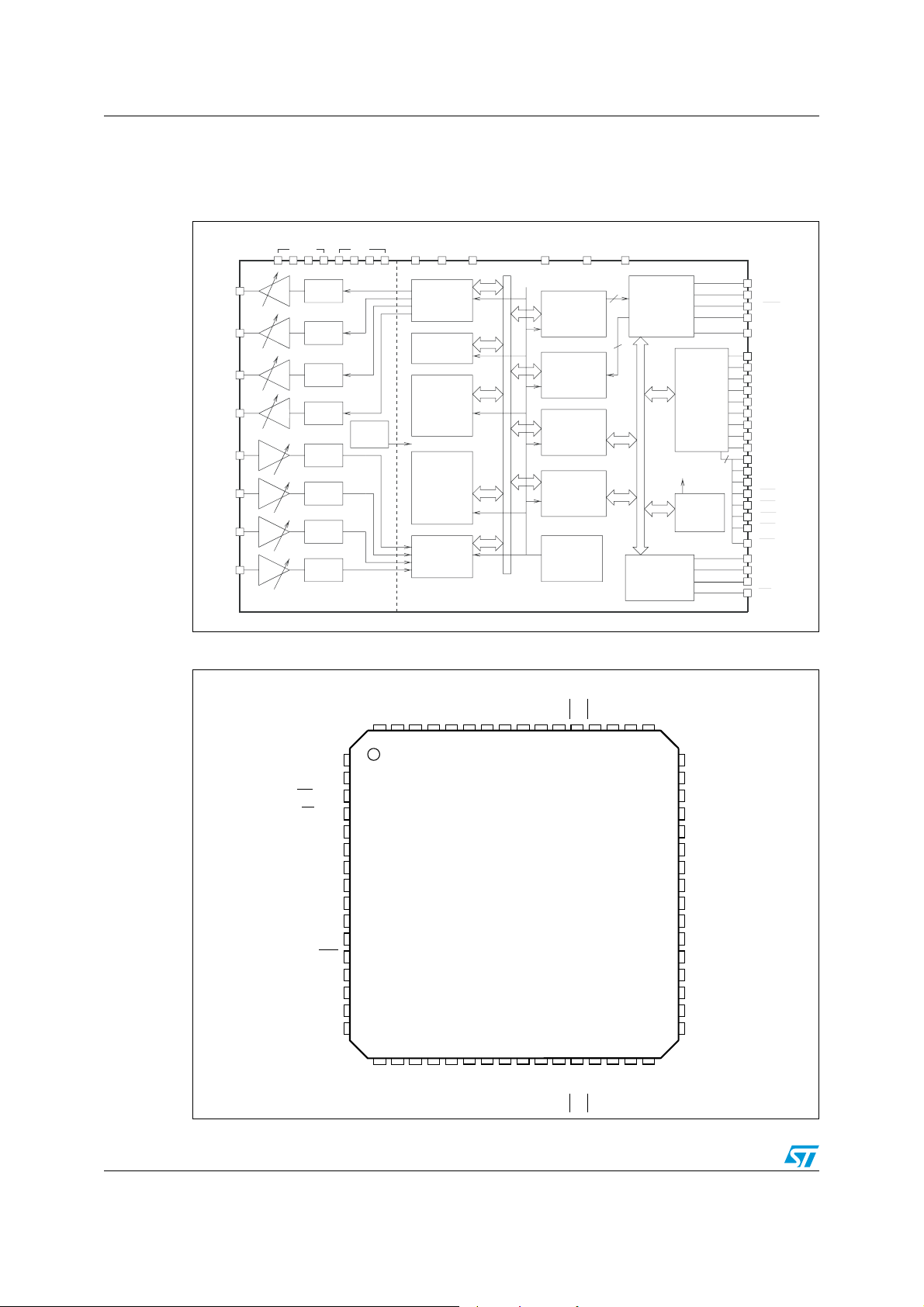
Figure 1. Block diagram . . . . . . . . . . . . . . . . . . . . . . . . . . . . . . . . . . . . . . . . . . . . . . . . . . . . . . . . . . . . 6
Figure 2. Pin connection (top view) . . . . . . . . . . . . . . . . . . . . . . . . . . . . . . . . . . . . . . . . . . . . . . . . . . . 6
Figure 3. Transmit path . . . . . . . . . . . . . . . . . . . . . . . . . . . . . . . . . . . . . . . . . . . . . . . . . . . . . . . . . . . 13
Figure 4. Receive path . . . . . . . . . . . . . . . . . . . . . . . . . . . . . . . . . . . . . . . . . . . . . . . . . . . . . . . . . . . . 13
Figure 5. MCU mode: time slot assignment . . . . . . . . . . . . . . . . . . . . . . . . . . . . . . . . . . . . . . . . . . . . 13
Figure 6. Pin-strap mode: time slot assignment. . . . . . . . . . . . . . . . . . . . . . . . . . . . . . . . . . . . . . . . . 15
Figure 7. Typical application circuit with STLC3080 without metering pulse injection and I/O pins
in dynamic mode. . . . . . . . . . . . . . . . . . . . . . . . . . . . . . . . . . . . . . . . . . . . . . . . . . . . . . . . . 40
Figure 8. Pin-strap mode short frame sync. timing . . . . . . . . . . . . . . . . . . . . . . . . . . . . . . . . . . . . . . 43
Figure 9. Pin-strap mode long frame sync. timing . . . . . . . . . . . . . . . . . . . . . . . . . . . . . . . . . . . . . . . 44
Figure 10. MCU mode frame sync. timing . . . . . . . . . . . . . . . . . . . . . . . . . . . . . . . . . . . . . . . . . . . . . . 44
Figure 11. Serial control port timing . . . . . . . . . . . . . . . . . . . . . . . . . . . . . . . . . . . . . . . . . . . . . . . . . . . 44
Figure 12. SLIC control port timing . . . . . . . . . . . . . . . . . . . . . . . . . . . . . . . . . . . . . . . . . . . . . . . . . . . 45
Figure 13. LQFP64 (10 x 10 x 1.4 mm) mechanical data and package dimensions . . . . . . . . . . . . . . 49
Doc ID 7052 Rev 5 5/51
Block diagram and pin connection STLC5046
1 Block diagram and pin connection
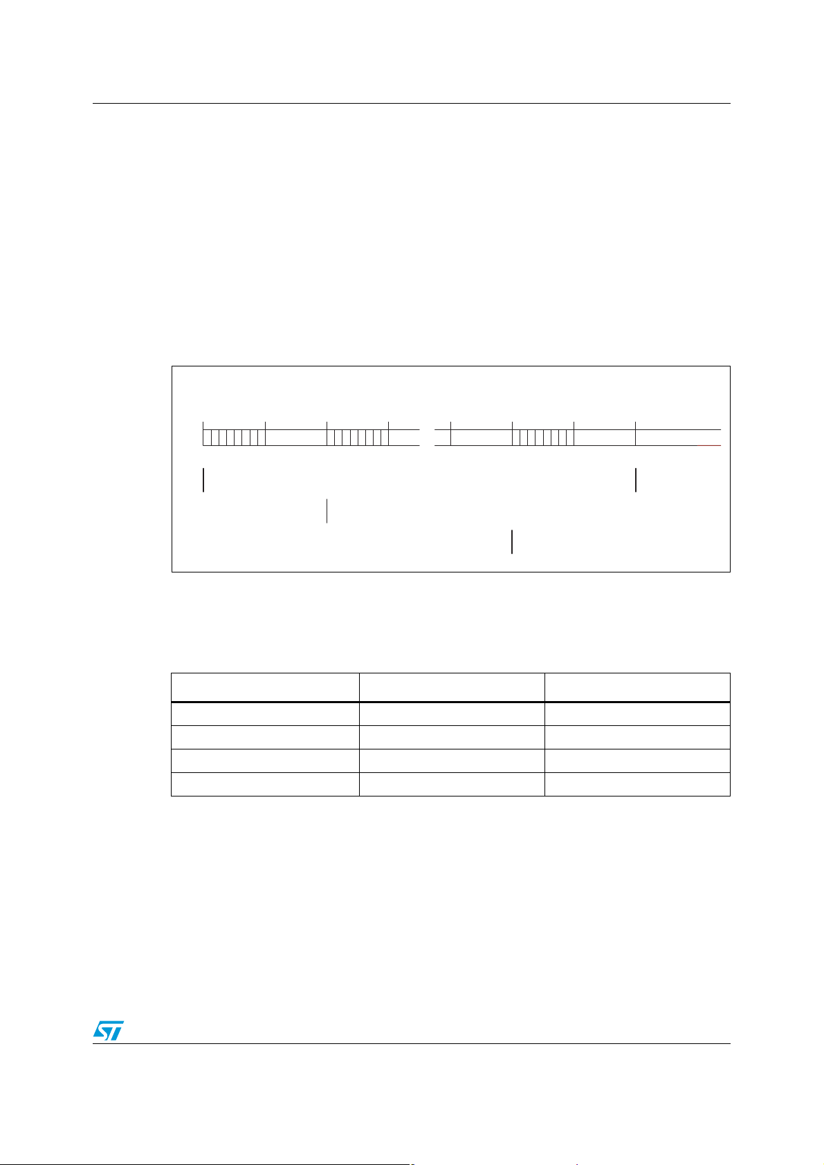
Figure 1. Block diagram
VFRO0
VFRO1
VFRO2
VFRO3
VFXI0
VFXI1
VFXI2
VFXI3
GX0
GX1
GX2
GX3
GR0
GR0
GR1
GR0
GR2
GR0
GR3
GR0
Post
Filter
Post
Filter
Post
Filter
Post
Filter
Anti-Alias
A/D
Anti-Alias
A/D
Anti-Alias
A/D
Anti-Alias
A/D
VEEVCC
PLL
VDD VSS SUB
D/A
sigma-delta
INTERPOLATORS
RX FILTERS
TX FILTERS
DECIMATORS
Figure 2. Pin connection (top view)
DIGITAL PROCESSORANALOG FRONTEND
data
17-bit Bus
contlol
CAP
A/u Law
ENCODER
A/u Law
DECODER
PROGRAMMABLE
GAIN RX
PROGRAMMABLE
GAIN TX
ARBITER
M0M1
8bit
PCM
INTERFACE
& SLOT ASSGN
8bit
8-bit Bus
to analog FE
Programmable functions
SERIAL
CONTROL
INTERFACE
SLIC
CONTROL
PORT
CONFIG.
REGISTERS
FS/FS0
MCLK
TSX
DX
DR
IO11
IO10
IO9
IO8
IO7
IO6 / FS3
IO5 / FS2
IO4 / FS1
IO3 / PD3
IO2 / GR3
IO1 / PD2
IO0 / GR2
CS3 / GX3
CS2 / GX2
CS1 / GX1
CS0 / GX0
INT / AMU
CCLK / GR1
CI / PD0
CO / GR0
CS / PD1
IO9
IO10
IO11
59 58 57 565455 53 52 51 50 49
RES
RES
INT/AMU
CS/PD1
CO/GR0
CI/PD0
CCLK/GR1
VSS
VDD
DR
IO8
IO7
IO6/FS3
RES
N.C.
60
61
62
63
64
1
2
3
4
5
6
7
8
9
10
DX
12
TSX
13
MCLK
N.C.
N.C.
14
15
16
17 18 19 20 21
N.C.
N.C.
IO1/PD2
IO0/GR2
22 23 24 25 26
IO4/FS1
IO5/FS2
IO3/PD3
IO2/GR3
FS/FS0
6/51 Doc ID 7052 Rev 5
VCC4M1VEE4
CS2/GX2
271128 29 30 31 32
M0
VEE5
VCC5
CS0/GX0
CS3/GX3
VEE2
VEE1
CS1/GX1
VEE3
VEE0
N.C.
N.C.
48
47
46
45
44
43
42
41
40
39
38
37
36
35
34
33
VFRO3
N.C.
VFXI3
VCC3
VCC2
VFXI2
VFRO2
SUB
CAP
VFRO1
VFXI1
VCC1
VCC0
VFXI0
N.C.
VFRO0
D98TL405
STLC5046 Block diagram and pin connection
1.1 Pin description
Table 2. I/O definition
Type Definition
AI Analog input
AO Analog output
ODO Open drain output
DI Digital input
DO Digital output
DIO Digital input/output
DTO Digital tristate output
DPS Digital power supply
APS Analog power supply
Table 3. Pin description
N. Name Type Function
Analog
33 VFRO0 AO
39 VFRO1 AO
Receive analog amplifier output channel 0. PCM data received on the programmed
time slot on DR input is decoded and appears at this output.
Receive analog amplifier output channel 1. PCM data received on the programmed
time slot on DR input is decoded and appears at this output.
42 VFRO2 AO
48 VFRO3 AO
Receive analog amplifier output channel 2. PCM data received on the programmed
time slot on DR input is decoded and appears at this output.
Receive analog amplifier output channel 3. PCM data received on the programmed
time slot on DR input is decoded and appears at this output.
35 VFXI0 AI TX Input amplifier channel 0. Typ 1M.input impedance
38 VFXI1 AI TX Input amplifier channel 1. Typ 1M.input impedance
43 VFXI2 AI TX Input amplifier channel 2. Typ 1M.input impedance
46 VFXI3 AI TX Input amplifier channel 3. Typ 1M.input impedance
40 CAP AI
AGND voltage filter pin. A 100nF capacitor must be connected between ground and
this pin.
Power supply
25, 36,
37, 44,
45, 56,
26,30,
31, 50,
51,55
VCC/0/1/2
/3/ 4/5
VEE/0/1/2
/3/ 4/5
APS
Total 6 pins: 3.3 V analog power supplies, should be shorted together, require
100nF decoupling capacitor to VEE.
APS Total 6 pins: analog ground, should be shorted together.
9 VDD DPS Digital power supply 3.3 V, require 100 nF decoupling capacitor to VSS.
8 VSS DPS Digital ground
Doc ID 7052 Rev 5 7/51
Block diagram and pin connection STLC5046
Table 3. Pin description (continued)
N. Name Type Function
41 SUB DPS
Substrate connection. Must be shorted together with VEE and VSS pins as close as
possible the chip.
Not connected
15, 16,
17, 18,
32, 34,
N.C. Not connected.
47, 49,
64
1,2,63 RES Reserved: must be left not connected.
Digital
27 M0 DI Mode select, see M1
M1 M0 Mode select
54 M1 DI
0
1
0
1
Pin-strap mode: basic functions selected by proper pin strapping
1
MCU mode: device controlled via serial interface
0
Reset status
0
Not allowed
1
Master clock input. Four possible frequencies can be used: 1.536/1.544 MHz;
13 MCLK DI
2.048 MHz; 4.096 MHz; 8.192 MHz. The device automatically detect the frequency
applied. This signal is also used as bit clock and it is used to shift data into and out
of the DR and DX pins.
Transmit time slot (open drain output, 3.2mA). Normally it is floating in high
12 TSX
ODO
impedance state except when a time slot is active on the DX output. In this case
output pulls low to enable the backplane line driver.
TSX
Transmit PCM interface. It remains in high impedance state except during the
11 DX DTO
assigned time slots during which the PCM data byte is shifted out on the rising edge
of MCLK.
10 DR DI
Receive PCM interface. It remains inactive except during the assigned receive time
slots during which the PCM data byte is shifted in on the falling edge of MCLK.
SLIC control I/O pin #7. Can be programmed as input or output via DIR register.
61 IO7 DIO
Depending on content of CONF register can be a static input/output or a dynamic
input/output synchronized with the CSn
60 IO8 DIO SLIC control I/O pin #8. (see IO7 description).
59 IO9 DIO SLIC control I/O pin #9. (see IO7 description).
58 IO10 DIO SLIC control I/O pin #10. (see IO7 description).
57 IO11 DIO SLIC control I/O pin #11. (see IO7 description).
Digital (dual mode)
8/51 Doc ID 7052 Rev 5
output signals controlling the SLICs.
STLC5046 Block diagram and pin connection
Table 3. Pin description (continued)
N. Name Type Function
MCU control mode: FS.
Frame Sync. Pulse. A pulse or a square wave waveform with an 8kHz repetition
rate is applied to this pin to define the start of the receive and transmit frame.
14 FS/FS0 DI
19 IO0/GR2 DIO/DI
20 IO1/PD2 DIO/DI
Effective start of the frame can be then shifted of up to 7 clock pulses independently
in receive and transmit directions by proper programming of the PCMSH register.
Pin-strap control mode: FS0.
Frame Sync. pulse of channel #0. One MCLK cycle long, starts PCM data transfer
in the Time Slot following its falling edge (Short Frame Delayed Timing).
MCU control mode: IO0.
Slic control I/O pin #0. Can be programmed as input or output via DIR register.
Depending on content of CONF register can be a static input/output or a dynamic
input/output synchronized with the CSn
Pin-strap control mode: GR2.
Receive gain programming channel 2:
1: Receive gain = -0.8 dB
0: Rec. gain = -4.3 dB
MCU control mode: IO1.
Slic control I/O pin #1. (see IO0 description).
Pin-strap control mode: PD2.
Power Down command channel 2:
1: Channel 2 Codec is in power down.
(equivalent to CONF reg bit2 = 1)
0: Channel 2 Codec is in power up.
(equivalent to CONF reg. bit2 = 0)
output signals controlling the SLICs.
21 IO2/GR3 DIO/DI
22 IO3/PD3 DIO/DI
23 IO4/FS1 DIO/DI
24 IO5/FS2 DIO/DI
MCU control mode: IO2.
Slic control I/O pin #2. (see IO0 description)
Pin-strap control mode: GR3.
Receive gain programming channel 3. (see GR2 description)
MCU control mode: IO3.
Slic control I/O pin #3. (see IO0 description).
Pin-strap control mode: PD3.
Power down command channel 3. (see PD2 description)
MCU control mode: IO4
Slic control I/O pin #4. (see IO0 description).
Pin-strap control mode: FS1.
Frame sync. pulse of channel #1. One MCLK cycle long, starts PCM data transfer in
the time slot following its falling edge (short frame delayed timing).
MCU control mode: IO4.
Slic control I/O pin #5. (see IO0 description).
Pin-strap control mode: FS2.
Frame sync. pulse of channel #1. One MCLK cycle long, starts PCM data transfer in
the time slot following its falling edge (short frame delayed timing).
Doc ID 7052 Rev 5 9/51
Block diagram and pin connection STLC5046
Table 3. Pin description (continued)
N. Name Type Function
MCU control mode: IO4.
Slic control I/O pin #6. (see IO0 description).
62 IO6/FS3 DIO/DI
28 CS0
29 CS1
53 CS2/GX2 DO/DI
/GX0 DO/DI
/GX1 DO/DI
Pin-strap control mode: FS3.
Frame sync. pulse of channel #1. One MCLK cycle long, starts PCM data transfer in
the time slot following its falling edge (short frame delayed timing).
MCU control mode: CS0.
Slic CS control #0.
Depending on CONF reg. content can be a CS output for SLIC #0 or a static I/O.
When configured as CS output it is automatically generated by the Codec with a
repetition time of 31.25 µs. In this mode also the IO11.0 are synchronized and carry
proper data in and out synchronous with CS.
Pin-strap control mode: GX0.
Transmit gain programming channel 0:
1: Transmit gain = 0 dB
0: Transmit gain = - 3.5 dB
MCU control mode: CS1
Slic CS control #1, (see CS0
Pin-strap control mode: GX1.
Transmit gain programming channel 1 (see GX0 description)
MCU control mode: CS2
Slic CS control #2, (see CS0
Pin-strap control mode: GX2.
Transmit gain programming channel 2 (see GX0 description)
:
description).
.
description).
MCU control mode: CS3
52 CS3
4CS
7
6CI/PD0DI/DI
/GX3 DO/DI
/PD1 DI/DI
CCLK/GR1
DI/DI
Slic CS control #3, (see CS0 description).
Pin-strap control mode: GX3.
Transmit gain programming channel 3 (see GX0 description)
MCU control mode: CS
Chip Select of Serial Control Bus. When this pin is low control information can be
written to or read from the device via the CI and CO pins.
Pin-strap control mode: PD1.
Power Down command channel 1. (see PD2 description).
MCU control mode: CCLK.
Clock of Serial Control Bus. This clock shifts serial control information into or out of
CI or CO when CS input is low depending on the current instruction. CCLK may be
asynchronous with the other system clocks.
Pin-strap control mode: GR1.
Receive gain programming ch. 1, (see GR2 description).
MCU control mode: CI.
Control Data Input of Serial Control Bus. Control data is shifted in the device when
CS
Pin-strap control mode: PD0.
Power Down command channel 0. (see PD2 description).
.
.
is low and clocked by CCLK.
10/51 Doc ID 7052 Rev 5
STLC5046 Block diagram and pin connection
Table 3. Pin description (continued)
N. Name Type Function
MCU control mode: CO.
Control Data Output of Serial Control Bus. Control data is shifted out the device
5 CO/GR0 DTO/DI
3INT
/AMU ODO/DI
when CS
H. I., valid data are shifted out during the following 8 CCLK pulses.
Pin-strap control mode: GR0.
Receive gain programming ch. 0, (see GR2 description).
MCU control mode: INT
Interrupt output (open drain), goes low when a data change has been detected in
the I/O pins. One mask registers allow to mask any I/O pin. Interrupt is reset when
the I/O register is read.
Pin-strap control mode: AMU.
A/µ Law selection:
AMU=0: µ Law
AMU=1: A Law, even bit inverted
is low and clocked by CCLK. During the first 8 CCLK pulses the CO pin is
.
Doc ID 7052 Rev 5 11/51

Functional description STLC5046
2 Functional description
2.1 Power on initialization
When power is first applied it is recommended to reset the device by forcing the condition
M1.0=00, in order to clear all the internal registers.
In MCU mode M0 is set steadily Low and the device is reset by applying a negative pulse to
M1 (its operative level in MCU mode is High); same result can be obtained by writing an
High level into the control bit RES of the CONF register.
In pin-strap mode M1 is set steadily Low and the device is reset by applying a negative
pulse to M0 (its operative level in pin-strap mode is High); at the end of the Reset phase
(M0=High) the device is programmed according to the logical configuration of the control
pins.
During the reset condition all the I/On and CS_n pins are set as inputs, DX is set in high
impedance and all VFROn outputs are forced to AGND.
2.2 Power down state
Each of the four channel may be put into power down mode by setting the appropriate bit in
the CONF register or strapping to VDD the proper pin. In this mode the eventual
programmed DX channel is set in high impedance while the VFRO outputs are forced to
AGND. In pin-strap mode the value forced on the input pin is internally updated every FS
signal.
2.3 Transmit path
The analog VFXI signal through an amplifier stage is applied to a PCM converter and the
corresponding digital signal is sent to DX output.
In MCU mode, the amplifier gain can be programmed with two different values by means of
TXG Reg.: 0 dB or +3.52 dB.
A programmable gain block after the A/D conversion allows to set transmit gain in 12dB
range, with steps <0.1dB by writing proper code into GTXn register.
Setting GTXn=00h, the transmitted signal is muted, i.e. an idle PCM signal is generated on
DX.
A/µ coding Law is selected by bit5 (AMU) of CONF reg.
Setting LIN=1 (bit6 of CONF reg.) the linear coding Law is selected (16bits); in this case the
signal sent on DX will take two adjacent PCM time slots.
In Pin-strap mode, the amplifier gain is set to 0dB; only two values of Transmit gain can be
selected according to the level of GXn control input (in Pin-strap):
GXn=1 selects the gain corresponding to GTXn=FFh (0 dB)
GXn=0 selects the gain corresponding to GTXn=8Fh (-3.5 dB)
Different gain value is obtained through proper voltage divider.
A/µ coding Law is selected according to AMU pin level:
12/51 Doc ID 7052 Rev 5
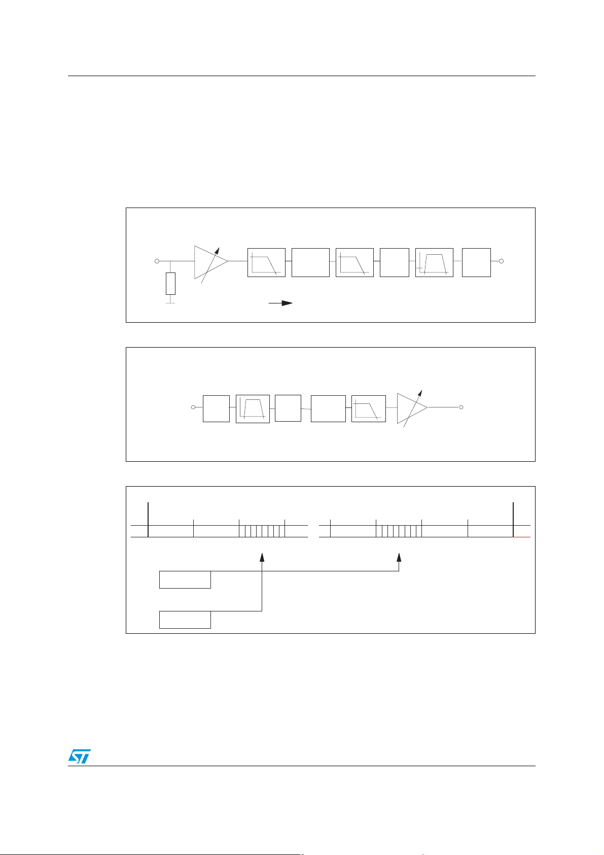
STLC5046 Functional description
AMU=0 µ Law selected.
AMU=1 A Law selected.
VFXI input must be AC coupled to the signal source; the voltage swing allowed is 1.0Vpp
when the preamplifier gain is set 0dB or 0.66Vpp if the gain is set to 3.52dB (MCU mode
only); higher levels must be reduced through proper dividers.
Typical impedance of VFXI input is 1Mohm.
Figure 3. Transmit path
TXG: 0dB
+3.52dB
VFXI
1M
AGND
Ω
for TXG=0dB; GX=0dB (FF)
-15dBm|
Ω
600
ΣΔ
conv.
0dBm0
GX
8 bit linear
1/4 to 1
A/
Figure 4. Receive path
RXG: 0dB
-1. 94dB
-4. 44dB
-7. 96dB
=> -3dBm |
-13.98d B
VFRO
600Ω
DR
A/
μ
GR
8 bit linear
1/4 to 1
ΣΔ
conv.
for RXG=0 dB; GR=0dB (FF)
0dBm0
Figure 5. MCU mode: time slot assignment
FS FS
TS0 TS23/31/61 /127
Receive Time Slot Transmit Time Slot
D7..................D0 D7...................D0
DX
μ
DXAn Reg.
DRAn Reg.
2.4 Receive path
The received PCM signal DR through the decoder section, the gain select block and the D/A
converter is converted in an analog signal which is transferred to VFRO output through an
amplifier stage.
Doc ID 7052 Rev 5 13/51

Functional description STLC5046
In MCU mode a programmable gain block before the A/D conversion allows to set receive
gain in 12dB range, with steps <0.1 dB by writing proper code into GRXn register.
The amplifier gain can be programmed with five different values by means of RXG register:
0dB -1.94dB -4.44dB -7.96dB -13.98dB.
Setting GRXn=00h, the receive signal is muted and VFRO output is set to AGND.
A/µ coding Law is selected by bit5 (AMU) of CONF reg.
Setting LIN = 1 (bit6 of CONF reg.) the linear coding Law is selected (16bits); in this case
the signal received on DR will take two adjacent PCM time slots.
In pin-strap mode only two values of Receive Gain can be selected according to the level of
GRn control input (in pin-strap) GRn = 1 selects the gain corresponding to GRXn= E2h,
RXG = 0dB (-0.8 dB) GRn = 0 selects the gain corresponding to GRXn = AFh,
RXG = -1.94 dB (-4.3 dB).
Different gain value is obtained through proper voltage divider.
A/µ coding Law is selected according to AMU pin level:
AMU=0 µ Law selected.
AMU=1 A Law selected.
VFRO output, referred to AGND must be AC coupled to the load, referred to VSS, to prevent
a DC current flow.
VFRO has a drive capability of 1.0mA (peak value), with a max AC swing of 2 Vpp.
In order to get the best noise performances it is recommended to keep the GRX value as
close as possible to the maximum (FFh) setting properly the additional attenuation by
means of RXG.
2.5 PCM interface
The STLC5046 dedicate five pins (six in pin-strap mode) to the interface with the PCM
highways.
MCLK represents the bit clock and is also used by the device as a source for the clock of the
internal Sigma Delta converter timings. Four possible frequencies can be used:
1.536/1.544 MHz (24 channels PCM frame); 2048 MHz (32 channels PCM frame);
4.096 MHz (64 channels PCM frame); 8.192 MHz (128 channels PCM frame).
The operating frequency is automatically detected by the device when both MCLK and FS
are applied. MCLK is synchronizing both the transmit data (DX) and the receive data (DR).
2.5.1 MCU mode
The Frame Sync. signal FS is the common time base for all the four channels; Short (one
MCLK period) or Long (more than one MCLK period) FS are allowed.
Transmit and Receive programmable Time-Slots are framed to an internal sync. signal that
can be coincident with FS or delayed of 1 to 7 MCLK cycles depending on the programming
of PCMSH register.
14/51 Doc ID 7052 Rev 5
STLC5046 Functional description
DX represent the transmit PCM interface. It remains in high impedance state except during
the assigned time slots during which the PCM data byte is shifted out on the rising edge of
MCLK.
The four channels can be shifted out in any possible timeslot as defined by the DXA0 to
DXA3 registers. If one codec is set in Power Down by software programming the
corresponding timeslot is set in High Impedance. When linear coding mode is selected by
CONF register programming the output channel will need two consecutive timeslots (see
register description).
DR represent the receive PCM interface. It remains inactive except during the assigned time
slots during which the PCM data byte is shifted in on the falling edge of MCLK. The four
channels are shifted in any possible timeslot as defined by the DRA0 to DRA3 registers.
Figure 6. Pin-strap mode: time slot assignment
Receive /Transmit
Time Slot
CH0 CHn CHm
D7...................D0
FS0
2.5.2 Pin-strap mode
When pin-strap mode is selected, dedicated Frame Sync. FS3..0 are provided on dual
function pins:
MCU Pin-strap Pin
FS FS0 14
IO4 FS1 23
IO5 FS2 24
IO6 FS3 62
The PCMSH register cannot be accessed, therefore the beginning of the transmit and
receive frame is identified by the rising edge of the FSn signal.
D7..................D0 D7...................D0
FSn
FSm
TS23/31 /61/ 127
Each channel has its dedicated Frame Sync. signal FSn. Short or Long frame timing is
automatically selected; depending on the FS signal applied to FS0 input. The assigned
Time Slot (Transmit and Receive) takes place in the 8 MCLK cycles following the falling
edge of FSn in case of Short Frame or the rising edge in case of Long Frame. If one codec
is set in Power Down by proper pin-strap configuration the corresponding timeslot is not
loaded and the VFRO output is kept at steady AGND level.
Doc ID 7052 Rev 5 15/51
Functional description STLC5046
Finally by means of the LOOPB register is possible to implement a digital or analog
loop_back on any of the selected channels.
TSX
represent the Transmit Time Slot (open drain output, 3.2mA). Normally it is floating in
high impedance state except when a time slot is active on the DX output. In this case TSX
output pulls low to enable the backplane line driver. Should be strapped to VSS when not
used.
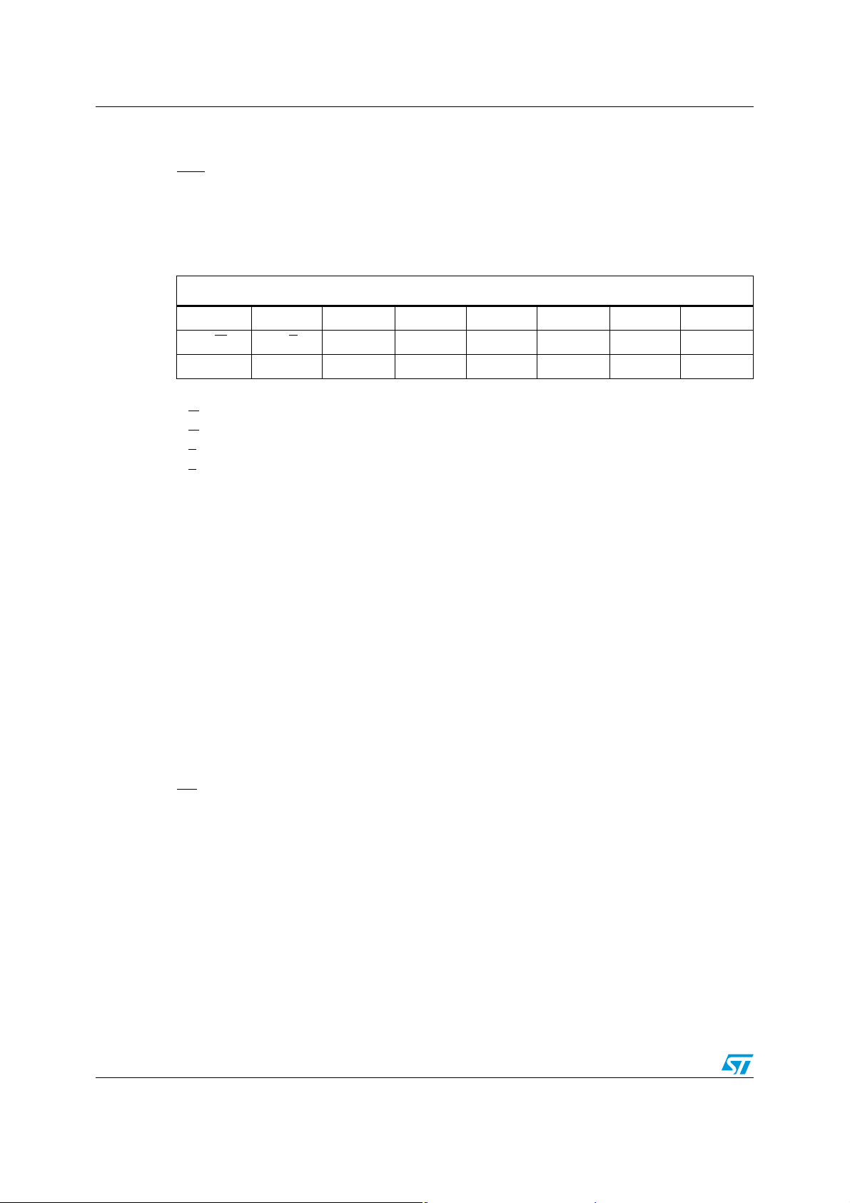
Table 4. Control byte structure
First byte (address)
7 6 5 4 3 2 1 0
R/W D/S A5 A4 A3 A2 A1 A0
D7 D6 D5 D4 D3 D2 D1 D0
R/W = 0: Write register
= 1: Read register
R/W
= 0: Single byte
D/S
= 1: Two bytes
D/S
A5..A0: Register Address
2.6 Control interface
STLC5046 has two control modes, a microprocessor control mode and a pin-strap control
mode. The two modes are selected by M0 and M1 pins. When M0 = low, M1 = high (MCU
control mode) the MCU port is activated; and the 41 registers of the device can be
programmed. When M0 = high, M1 = low (Pin-strap mode) the microprocessor control port
is disabled and some of the digital pins change their function allowing to perform a very
basic programming of the device.
In pin-strap mode the status of the control pins is entered at power-on reset and refreshed at
any Frame Sync. cycle.
In MCU mode the control information is written to or read from STLC5046 via the serial four
wires control bus:
CCLK: Control Clock
CS
: Chip Select input
CI: Serial Data input
CO: Serial Data output
All control instructions require 2 bytes, with the exception of the single byte for command
synchronization. The first byte specify the register address, and the type of access (Read or
Write). The second byte contain the data to be loaded into the register (on CI wire) or
carried out the register content (on CO wire) depending on the R/W bit of the first byte. CO
wire is normally in High Impedance and goes to low impedance only during the second byte
in case of Read operation. This allows to use a common wire for both CI/CO.
Serial data CI is shifted to the serial input register on the rising edge of CCLK and CO is
shifted out on the falling.
16/51 Doc ID 7052 Rev 5

STLC5046 Functional description
CS, normally High, is set Low during the transmission / reception of a byte, lasting 8CCLK
pulses.
Though, in general, two bytes of the same instruction take two CS
STLC5046 can handle the data transfer in a single 16 CCLK CS cycle, in both the directions.
One additional wire provided to the control interface is an open drain interrupt output (INT)
that goes low when a change of status is detected on the I/O pins.
2.7 SLIC control interface
The device provides 12 I/O pins plus 4 CS signals. The interface can work in dynamic or
static mode: it can be selected by means of DIR register.
● Dynamic Mode: the I/O pins are configured as input or output by means of DIR register.
The CS signals are used to select the different SLIC interface. In this case the I/O pin
can be multiplexed. The data loaded from SLIC#n via I/O pins configured as input can
be read in the DATAn register. The data written in a DATAn register will be loaded on the
I/O pins configured as output when the Csn signal will be active.
● Static Mode: The CS signal can be used as I/O pins. They can be configured as input
or output I/O by means of DATA1 register. The data corresponding to the CS signal can
be read or written by means of DATA2 register. All data related to th other I/O pins can
be read or written by means of DATA0 register.
separated cycles,
Doc ID 7052 Rev 5 17/51

Registers addresses STLC5046
3 Registers addresses
Table 5. Registers addresses (only MCU mode)
Address Name Description
00h CONF Configuration register
01h DIR-L I/O Direction (bit 7-0)
02h DIR-H I/O Direction (bit 11-8)
03h DATA0-L I/O Data ch#0/ Static Data; (bit 7-0)
04h DATA0-H I/O Data ch#0/ Static Data; (bit 11-8)
05h DATA1-L I/O Data ch#1 (bit 7-0) / CS Direction
06h DATA1-H I/O Data ch#1 (bit 11-8)
07h DATA2-L I/O Data ch#2 (bit 7-0) / CS Data
08h DATA2-H I/O Data ch#2 (bit 11-8)
09h DATA3-L I/O Data ch#3 (bit 7-0)
0Ah DATA3-H I/O Data ch#3 (bit 11-8)
0Bh GTX0 Transmit Gain ch#0
0Ch GTX1 Transmit Gain ch#1
0Dh GTX2 Transmit Gain ch#2
0Eh GTX3 Transmit Gain ch#3
0Fh GRX0 Receive Gain ch#0
10h GRX1 Receive Gain ch#1
11h GRX2 Receive Gain ch#2
12h GRX3 Receive Gain ch#3
13h DXA0 Transmit Timeslot ch#0
14h DXA1 Transmit Timeslot ch#1
15h DXA2 Transmit Timeslot ch#2
16h DXA3 Transmit Timeslot ch#3
17h DRA0 Receive Timeslot ch#0
18h DRA1 Receive Timeslot ch#1
19h DRA2 Receive Timeslot ch#2
1Ah DRA3 Receive Timeslot ch#3
1Bh PCMSH PCM Shift register
1Ch DMASK-L Interrupt Mask I/O Port (03h)
1Dh DMASK-H Interrupt Mask I/O Port (04h)
1Eh CMASK Interrupt Mask I/O Port (07h)
1Fh PCHK-A Persistency Check Time for Input A
20h PCHK-B Persistency Check Time for Input B
21h INT Interrupt register
22h ALARM Alarm register
23h AMASK Interrupt Mask for Alarm
24h LOOPB Loopback register
25h TXG Transmit Preamp. Gain
26h RXG-1,0 Receive Preamp. Gain (ch1 ch0)
27h RXG-3,2 Receive Preamp. Gain (ch3 ch2)
31h SRID Silicon Revision Identification Code
18/51 Doc ID 7052 Rev 5

STLC5046 Registers addresses
3.1 Registers description
3.1.1 Configuration register (CONF)
Addr=00h; Reset Value=3Fh
Bit7 Bit6 Bit5 Bit4 Bit3 Bit2 Bit1 Bit0
RES LIN AMU STA PD3 PD2 PD1 PD0
RES=0 Normal operation
RES=1 Device reset: I/0n and CSn
LIN=0 A or µ Law PCM encoding
LIN=1 Linear encoding (16 bits), two’s complement.
AMU=0 µ Law selection
AMU=1 A Law selection (even bits inverted)
STA=0 CS0
to CS3 scan the four SLICs connected to the I/O control port, each CS has a
31.25µs repetition time.
STA=1; I/O are static, CS0
to CS3 are configured as generic static I/O
PD3..0=0 CODEC 3..0 is active
PD3..0=1 CODEC 3..0 is in power Down. When one codec is in Power Down the
corresponding VFRO output is forced to AGND. and the corresponding transmit time slot on
DX is set in H.I.
Pin-strap value:
RES 0 AMU 0 PD3 PD2 PD1 PD0
3.1.2 I/O Direction register (DIR)
Addr=01h; Reset Value=00h
are all inputs, DX is H.I. (equivalent to Hw. reset).
Addr=02h; Reset Value=X0h
Bit7 Bit6 Bit5 Bit4 Bit3 Bit2 Bit1 Bit0
IO
7 IO6 IO5 IO4 IO3 IO2 IO1 IO0
IO11 IO10 IO9 IO8
IO11..0 = 0; I/O pin 11..0 is an input, data on the I/O input is written in DATAn register bit
11..0.
IO
11..0 = 1; I/O pin 11..0 is an output, data contained in DATAn register bit11..0 is transferred
to the I/O output.
Doc ID 7052 Rev 5 19/51

Registers addresses STLC5046
Pin-strap value:
00000000
00000000
3.1.3 I/O Data register channel #0 (DATA0)
Addr=03h; Reset Value=00h
Addr=04h; Reset Value=X0h
If bit 4 of CONF register (STA)=0
Dynamic I/O mode:
Bit7 Bit6 Bit5 Bit4 Bit3 Bit2 Bit1 Bit0
D0
7 D06 D05 D04 D03 D02 D01 D00
D011 D010 D09 D08
When CS0 is active D011..0 are transferred to the corresponding I/O pins configured as
outputs (see DIR register). For the I/O pins configured as inputs the corresponding D0
11..0
will be written by the values applied to those pins while CS0 is low.
If bit 4 of CONF register (STA)=1
Static I/O mode:
Bit7 Bit6 Bit5 Bit4 Bit3 Bit2 Bit1 Bit0
DS
7 DS6 DS5 DS4 DS3 DS2 DS1 DS0
DS11 DS10 DS9 DS8
D11..0 are transferred to the corresponding I/O pins configured as outputs (see DIR register).
For the I/O pins configured as inputs the corresponding D
11..0 will be written by the values
applied to those pins.
Pin-strap value:
0 0 0 0 0 0 0 0
0 0 0 0
3.1.4 I/O Data register channel #1 (DATA1)
Addr=05h; Reset Value=00h
Addr=06h; Reset Value=X0h
20/51 Doc ID 7052 Rev 5

STLC5046 Registers addresses
If bit 4 of CONF register (STA)=0
Dynamic I/O mode:
Bit7 Bit6 Bit5 Bit4 Bit3 Bit2 Bit1 Bit0
D1
7 D16 D15 D14 D13 D12 D11 D10
D111 D110 D19 D18
When CS1 is active D11..0 are transferred to the corresponding I/O pins configured as
outputs (see DIR register). For the I/O pins configured as inputs the corresponding D
be written by the values applied to those pins while CS1
is low.
11..0 will
If bit 4 of CONF register (STA)=1
Static I/O mode:
Bit7 Bit6 Bit5 Bit4 Bit3 Bit2 Bit1 Bit0
CIO
3 CIO2 CIO1 CIO0
CIO0..3=0 The CS0..3 is a static input, DATA is written in DATA2 register bits 0..3.
CIO0..3=1 The CS0..3
is a static output, DATA is taken from DATA2 register bits 0..3.
Pin-strap value:
00000000
3.1.5 I/O Data register channel #2 (DATA2)
Addr=07h; Reset Value=00h
Addr=08h; Reset Value=X0h
If bit 4 of CONF register (STA)=0
Dynamic I/O mode:
Bit7 Bit6 Bit5 Bit4 Bit3 Bit2 Bit1 Bit0
D2
7 D26 D25 D24 D23 D22 D21 D20
0000
D211 D210 D29 D28
When CS2 is active D211..0 are transferred to the corresponding I/O pins configured as
outputs (see DIR register). For the I/O pins configured as inputs the corresponding D11..0
will be written by the values applied to those pins while CS2
Doc ID 7052 Rev 5 21/51
is low.

Registers addresses STLC5046
If bit 4 of CONF register (STA)=1
Static I/O mode:
Bit7 Bit6 Bit5 Bit4 Bit3 Bit2 Bit1 Bit0
CD
3 CD2 CD1 CD0
CD3..0 are transferred to the corresponding CS pin if configured as static output (see register
DATA1). For the CS
pins configured as static inputs the corresponding CD3..0 will be written
by the values applied to those pins.
Pin-strap value:
00000000
0000
3.1.6 I/O Data register channel #3 (DATA3)
Addr=09h; Reset Value=00h
Addr=0Ah; Reset Value=X0h
Used only if bit 4 of CONF register (STA)=0; Dynamic
I/O mode:
Bit7 Bit6 Bit5 Bit4 Bit3 Bit2 Bit1 Bit0
D3
7 D36 D35 D34 D33 D32 D31 D30
D311 D310 D39 D38
When CS3 is active D11..0 are transferred to the corresponding I/O pins configured as
outputs (see DIR register). For the I/O pins configured as inputs the corresponding D11..0
will be written by the values applied to those pins while CS3
is low.
If bit4 of CONF register (STA)=1
Static I/O mode:
can be used as general purpose R/W registers, without any direct action on the control of
the device.
Pin-strap value:
00000000
22/51 Doc ID 7052 Rev 5
0000

STLC5046 Registers addresses
3.1.7 Transmit Gain channel #0 (GTX0)
Addr=0Bh; Reset Value=00h
Bit7 Bit6 Bit5 Bit4 Bit3 Bit2 Bit1 Bit0
00h:Stop any transmit signal, null level is transmitted in the corresponding timeslot on DX
output.
>00h:Digital gain is inserted in the TX path equal to:
20log[0.25+0.75*(progr. value/256)]
Pin-strap values:
GX0=1: 0 dB gain (value = FFh):
11111111
GX0=0: -3.5 dB gain (value = 8Fh):
10001111
3.1.8 Transmit Gain channel #1 (GTX1)
Addr=0Ch; Reset Value=00h
Bit7 Bit6 Bit5 Bit4 Bit3 Bit2 Bit1 Bit0
00h:Stop any transmit signal, null level is transmitted in the corresponding timeslot on DX
output.
>00h:Digital gain is inserted in the TX path equal to:
20log[0.25+0.75*(progr. value/256)]
Pin-strap values:
GX0=1: 0 dB gain (value = FFh):
11111111
GX0=0: -3.5 dB gain (value = 8Fh):
Doc ID 7052 Rev 5 23/51

Registers addresses STLC5046
10001111
3.1.9 Transmit Gain channel #2 (GTX2)
Addr=0Dh; Reset Value=00h
Bit7 Bit6 Bit5 Bit4 Bit3 Bit2 Bit1 Bit0
00h: Stop any transmit signal, null level is transmitted in the corresponding timeslot on DX
output.
>00h:Digital gain is inserted in the TX path equal to:
20log[0.25+0.75*(progr. value/256)]
Pin-strap values:
GX0=1: 0 dB gain (value = FFh):
11111111
GX0=0: -3.5 dB gain (value = 8Fh):
10001111
3.1.10 Transmit Gain channel #3 (GTX3)
Addr=0Eh; Reset Value=00h
Bit7 Bit6 Bit5 Bit4 Bit3 Bit2 Bit1 Bit0
00h:Stop any transmit signal, null level is transmitted in the corresponding timeslot on DX
output.
>00h:Digital gain is inserted in the TX path equal to:
20log[0.25+0.75*(progr. value/256)]
Pin-strap values:
GX0=1: 0 dB gain (value = FFh):
11111111
24/51 Doc ID 7052 Rev 5

STLC5046 Registers addresses
GX0=0: -3.5 dB gain (value = 8Fh):
10001111
3.1.11 Receive Gain channel #0 (GRX0)
Addr=0Fh; Reset Value=00h
Bit7 Bit6 Bit5 Bit4 Bit3 Bit2 Bit1 Bit0
00h:Stop any received signal, AGND level is forced on the VFRO0 analog output.
>00h:Digital gain is inserted in the RX path equal to:
20log[0.25+0.75*(progr. value/256)]
Pin-strap values:
GR0=1: -0.8 dB gain (value = E2h):
11100010
GR0=0: -2.36 dB gain (value = AFh):
10101111
Overall gain including also RXG:
GR0 = 1:-0.8 dB; GR0 = 0: -4.3 dB
3.1.12 Receive Gain channel #1 (GRX1)
Addr=10h; Reset Value=00h
Bit7 Bit6 Bit5 Bit4 Bit3 Bit2 Bit1 Bit0
00h:Stop any received signal, AGND level is forced on the VFRO1 analog output.
>00h:Digital gain is inserted in the RX path equal to:
20log[0.25+0.75*(progr. value/256)]
Pin-strap values:
GR1=1: -0.8 dB gain (value = E2h):
Doc ID 7052 Rev 5 25/51

Registers addresses STLC5046
11100010
GR1=0: -2.36 dB gain (value = AFh):
10101111
Overall gain including also RXG:
GR1= 1:-0.8 dB; GR1 = 0: -4.3 dB
3.1.13 Receive Gain channel #2 (GRX2)
Addr=11h; Reset Value=00h
Bit7 Bit6 Bit5 Bit4 Bit3 Bit2 Bit1 Bit0
00h:Stop any received signal, AGND level is forced on the VFRO2 analog output.
>00h:Digital gain is inserted in the RX path equal to:
20log[0.25+0.75*(progr. value/256)]
Pin-strap values:
GR2=1: -0.8 dB gain (value = E2h):
11100010
GR2=0: -2.36 dB gain (value = AFh):
10101111
Overall gain including also RXG:
GR2 = 1:-0.8 dB; GR2 = 0: -4.3 dB
3.1.14 Receive Gain channel #3 (GRX3)
Addr=12h; Reset Value=00h
26/51 Doc ID 7052 Rev 5

STLC5046 Registers addresses
Bit7 Bit6 Bit5 Bit4 Bit3 Bit2 Bit1 Bit0
00h:Stop any received signal, AGND level is forced on the VFRO3 analog output.
>00h:Digital gain is inserted in the TX path equal to:
20log[0.25+0.75*(progr. value/256)]
Pin-strap values:
GR3=1: -0.8 dB gain (value = E2h):
11100010
GR3=0: -4.3 dB gain (value = AFh):
10101111
Overall gain including also RXG:
GR3 = 1:-0.8 dB; GR3 = 0: -4.3 dB
3.1.15 Transmit Time Slot channel #0 (DXA0)
Addr=13h; Reset Value=00h
Bit7 Bit6 Bit5 Bit4 Bit3 Bit2 Bit1 Bit0
EN0 T06 T05 T04 T03 T02 T01 T00
EN0=0: Selected transmit time slot on DX output is in H.I.
EN0=1: Selected transmit time slot on DX output is active carrying out the PCM encoded
signal of VFXI0.
T06..0: Define time slot number (0 to 127) on which PCM encoded signal of VFXI0 is carried
out.
If linear mode is selected (LIN=1 of CONF register) the 16 bits will be carried out as follows:
the 8 most significative bits in the programmed time slot, the 8 least significative bits in the
following timeslot.
Example: if T06..T00=00:
TS0 TS1
15 14 13 12 11 10 9 8 7 6 5 4 3 2 1 0
Doc ID 7052 Rev 5 27/51

Registers addresses STLC5046
Pin-strap value (value 80h):
10000000
Referred to FS0.
28/51 Doc ID 7052 Rev 5

STLC5046 Registers addresses
3.1.16 Transmit Time Slot channel#1 (DXA1)
Addr=14h; Reset Value=00h
Bit7 Bit6 Bit5 Bit4 Bit3 Bit2 Bit1 Bit0
EN1 T16 T15 T14 T13 T12 T11 T10
EN1=0: Selected transmit time slot on DX output is in H.I.
EN1=1: Selected transmit time slot on DX output is active carrying out the PCM encoded
signal of VFXI1.
T16..0:Define time slot number (0 to 127) on which PCM encoded signal of VFXI1 is carried
out.
If linear mode is selected (LIN=1 of CONF register) the 16 bits will be carried out as follows:
the 8 most significative bits in the programmed time slot, the 8 least significative bits in the
following timeslot.
Example: if T16..T10=00:
TS0 TS1
15 14 13 12 11 10 9 8 7 6 5 4 3 2 1 0
Pin-strap value (value 80h):
10000000
Referred to FS1.
3.1.17 Transmit Time Slot channel #2 (DXA2)
Addr=15h; Reset Value=00h
Bit7 Bit6 Bit5 Bit4 Bit3 Bit2 Bit1 Bit0
EN2 T26 T25 T24 T23 T22 T21 T20
EN2=0: Selected transmit time slot on DX output is in H.I.
EN2=1: Selected transmit time slot on DX output is active carrying out the PCM encoded
signal of VFXI2.
T26..0:Define time slot number (0 to 127) on which PCM encoded signal of VFXI2 is carried
out.
Doc ID 7052 Rev 5 29/51

Registers addresses STLC5046
If linear mode is selected (LIN=1 of CONF register) the 16 bits will be carried out as follows:
the 8 most significative bits in the programmed time slot, the 8 least significative bits in the
following timeslot.
Example: if T26..T20=00:
TS0 TS1
15 14 13 12 11 10 9 8 7 6 5 4 3 2 1 0
Pin-strap value (value 80h):
10000000
Referred to FS2.
3.1.18 Transmit Time Slot channel #3 (DXA3)
Addr=16h; Reset Value=00h
Bit7 Bit6 Bit5 Bit4 Bit3 Bit2 Bit1 Bit0
EN3 T36 T35 T34 T33 T32 T31 T30
EN3=0: Selected transmit time slot on DX output is in H.I.
EN3=1: Selected transmit time slot on DX output is active carrying out the PCM encoded
signal of VFXI3.
T36..0:Define time slot number (0 to 127) on which PCM encoded signal of VFXI3 is carried
out.
If linear mode is selected (LIN=1 of CONF register) the 16 bits will be carried out as follows:
the 8 most significative bits in the programmed time slot, the 8 least significative bits in the
following timeslot.
Example: if T36..T30=00:
TS0 TS1
15 14 13 12 11 10 9 8 7 6 5 4 3 2 1 0
Pin-strap value (value 80h):
10000000
Referred to FS3.
30/51 Doc ID 7052 Rev 5

STLC5046 Registers addresses
3.1.19 Receive Time Slot channel #0 (DRA0)
Addr=17h; Reset Value=00h
Bit7 Bit6 Bit5 Bit4 Bit3 Bit2 Bit1 Bit0
EN0 R06 R05 R04 R03 R02 R01 R00
EN0=0: Disable reception of selected time slot.
EN0=1: Selected receive time slot on DR input is PCM decoded and transferred to VFRO0
output.
R06..0:Define receive time slot number (0 to 127) on carrying the PCM signal to be decoded
and transferred to VFRO0 output.If linear mode is selected (LIN=1 of CONF register) the 16
bits will be used as linear code as follows: the 8most significative bits in the programmed
time slot, the 8 least significative bits in the following timeslot.
Example: if R06..R00=00:
TS0 TS1
15 14 13 12 11 10 9 8 7 6 5 4 3 2 1 0
Pin-strap value (value 80h):
10000000
Referred to FS0.
3.1.20 Receive Time Slot channel #1 (DRA1)
Addr=18h; Reset Value=00h
Bit7 Bit6 Bit5 Bit4 Bit3 Bit2 Bit1 Bit0
EN0 R16 R15 R14 R13 R12 R11 R10
EN1=0: Disable reception of selected time slot.
EN1=1: Selected receive time slot on DR input is PCM decoded and transferred to VFRO1
output.
R16..0:Define receive time slot number (0 to 127) on carrying the PCM signal to be decoded
and transferred to VFRO1 output.If linear mode is selected (LIN=1 of CONF register) the 16
bits will be used as linear code as follows: the 8most significative bits in the programmed
time slot, the 8 least significative bits in the following timeslot.
Example: if R16..R10=00:
Doc ID 7052 Rev 5 31/51

Registers addresses STLC5046
TS0 TS1
15 14 13 12 11 10 9 8 7 6 5 4 3 2 1 0
Pin-strap value (value 80h):
10000000
Referred to FS1.
3.1.21 Receive Time Slot channel #2 (DRA2)
Addr=19h; Reset Value=00h
Bit7 Bit6 Bit5 Bit4 Bit3 Bit2 Bit1 Bit0
EN0 R26 R25 R24 R23 R22 R21 R20
EN2=0: Disable reception of selected time slot.
EN2=1: Selected receive time slot on DR input is PCM decoded and transferred to VFRO1
output.
R26..0:Define receive time slot number (0 to 127) on carrying the PCM signal to be decoded
and transferred to VFRO2 output.If linear mode is selected (LIN=1 of CONF register) the 16
bits will be used as linear code as follows: the 8most significative bits in the programmed
time slot, the 8 least significative bits in the following timeslot.
Example: if R26..R20=00:
TS0 TS1
15 14 13 12 11 10 9 8 7 6 5 4 3 2 1 0
Pin-strap value (value 80h):
10000000
Referred to FS2.
3.1.22 Receive Time Slot channel #3 (DRA3)
Addr=1Ah; Reset Value=00h
Bit7 Bit6 Bit5 Bit4 Bit3 Bit2 Bit1 Bit0
EN0 R36 R35 R34 R33 R32 R31 R30
32/51 Doc ID 7052 Rev 5

STLC5046 Registers addresses
EN3=0: Disable reception of selected time slot.
EN3=1: Selected receive time slot on DR input is PCM decoded and transferred to VFRO1
output.
R36..0:Define receive time slot number (0 to 127) on carrying the PCM signal to be decoded
and transferred to VFRO2 output.If linear mode is selected (LIN=1 of CONF register) the 16
bits will be used as linear code as follows: the 8most significative bits in the programmed
time slot, the 8 least significative bits in the following timeslot.
Example: if R36..R30=00:
TS0 TS1
15 14 13 12 11 10 9 8 7 6 5 4 3 2 1 0
Pin-strap value (value 80h):
10000000
Referred to FS3.
3.1.23 PCM Shift register (PCMSH)
Addr=1Bh; Reset Value=00h
Bit7 Bit6 Bit5 Bit4 Bit3 Bit2 Bit1 Bit0
XS2 XS1 XS0 RS2 RS1 RS0
XS2..0:Effective start of the TX frame is the programmed values of clock pulses (0 to 7) after
the FS rising edge.
RS2..0:Effective start of the RX frame is the programmed values of clock pulses (0 to 7)
after the FS rising edge.
Pin-strap value (value=00h):
00000000
3.1.24 Interrupt Mask register for I/O port (DMASK)
Addr=1Ch; Reset Value=FFh
Addr=1Dh; Reset Value=XFh
Bit7 Bit6 Bit5 Bit4 Bit3 Bit2 Bit1 Bit0
Doc ID 7052 Rev 5 33/51

Registers addresses STLC5046
MD7 MD6 MD5 MD4 MD3 MD2 MD1 MD0
MD11 MD10 MD9 MD8
MD11..0=1: The corresponding I/O doesn’t generate interrupt.
MD11..0=0: The corresponding I/O (programmed as Input) generate interrupt if a change of
status is detected.
Input lines with persistency check generate interrupt if the changed status remains stable
longer than the time programmed in the persistency check registers PCHKA/B. Lines
without persistence check generate an immediate interrupt request.
Mask register has no effect on those pins configured as outputs, those pins will not generate
interrupt.
Pin-strap value.
11111111
1111
3.1.25 Interrupt Mask register for CD port (CMASK)
Addr=1Eh; Reset Value=XFh
Bit7 Bit6 Bit5 Bit4 Bit3 Bit2 Bit1 Bit0
MC3 MC2 MC1 MC0
In MCU mode, dynamic I/O configuration, MCn bits are the disable/enable interrupt related
to the channel n:
MC3..0= 0 Any I/O line of the related channel is enabled to generate interrupt depending on
DMASK setting.
MC3..0=1 Any I/O line of the related channel is disabled to generate interrupt independently
of DMASK setting.
In MCU mode, static I/O configuration, MCn bits are the interrupt mask bits related to CSn
that are configured as I/O lines.
MC3..0=1: The corresponding I/O doesn’t generate interrupt.
MC3..0=0: The corresponding I/O generate interrupt if a change of status is detected.
Input lines with persistency check generate interrupt if the changed status remains stable
longer than the time programmed in the persistency check registers PCHKA/B
Lines without persistency check generate an immediate interrupt request.
Mask register has no effect on those pins configured as outputs, those pins will not generate
interrupt.
34/51 Doc ID 7052 Rev 5

STLC5046 Registers addresses
Pin-strap value (value=00h):
11111111
3.1.26 Persistency Check register (PCHK-A/B)
Two input signals per channel, labeled A and B, are submitted to persistency check.
In dynamic mode (STA=0), A and B inputs of the four channels, are sampled on the
multiplexed lines IO0 (pin13) and IO1 (pin14).
In static mode (STA=1) the persistency check is performed on four pairs of lines, assigned to
each channel according to the table:
CHAN# Input A Input B
0 IO0 (pin 19) IO1 (pin 20)
1 IO4 (pin 17) IO5 (pin 18)
2 IO6 (pin 48) IO7 (pin 47)
3 IO10 (pin 44) IO11 (pin 43)
Addr=1Fh; Reset Value=00h
Addr=20h; Reset Value=00h
Bit7 Bit6 Bit5 Bit4 Bit3 Bit2 Bit1 Bit0
TA7 TA6 TA5 TA4 TA3 TA2 TA1 TA0
TB7 TB6 TB5 TB4 TB3 TB2 TB1 TB0
TA7..0 and TB7..0, content of PCHKA and PCHKB registers, define the minimum duration of
input A and B to generate interrupt; spurious transitions shorter than the programmed value
are ignored.
The time width can be calculated according to the formula:
Time-Width A = (TA7..0) x 64 µs
Time-Width B = (TB7..0) x 64 µs
If PCHKA/B is programmed to 00h the persistency check is not performed and any detected
transition will generate interrupt.
All the inputs, with or without persistency check, are sampled with a repetition rate of 32µs
Pin-strap value:
00000000
Doc ID 7052 Rev 5 35/51

Registers addresses STLC5046
00000000
3.1.27 Interrupt register (INT)
Addr=21h; Reset Value=00h
Bit7 Bit6 Bit5 Bit4 Bit3 Bit2 Bit1 Bit0
ICKF ID3 ID2 ID1 ID0
ICKF = 1: If interrupt is generated by a change of bit 0 in register ALARM.
In dynamic I/O configuration the ID3..0 bits latch the interrupt request from the related
channel.
Any single bit IDn is cleared after reading related I/O register or by setting MCn bit High (i.e.
when channel n is disabled to generate interrupt).
In static I/O configuration ID0 and ID2 bits latch the interrupt request from I/O11..0 and
CS3..0 respectively:
ID0: is set High when the interrupt is requested from any the I/O11..0 lines.
ID2: is set High when the interrupt is requested from any of the CS3..0 (configured as I/O).
ID0 and ID2 are cleared after reading related I/O register.
ID1 and ID3 are don’t care.
Pin-strap value (value=00b):
3.1.28 Alarm register (ALARM)
Addr=22h; Reset Value=00h
Bit7 Bit6 Bit5 Bit4 Bit3 Bit2 Bit1 Bit0
CKF=1: If number of PCM clock pulses in one frame period does not match expected value.
POR=1: If a Power On Reset is detected during operation.
The register ALARM is cleared after reading operation only if signals are inactive.
Pin-strap value (value=00h):
00000
POR CKF
00
36/51 Doc ID 7052 Rev 5

STLC5046 Registers addresses
3.1.29 Interrupt Mask register for Alarm (AMASK)
Addr=23h; Reset Value=11b
Bit7 Bit6 Bit5 Bit4 Bit3 Bit2 Bit1 Bit0
MCF
MCF=1: The corresponding alarm bit (CKF) doesn’t generate interrupt.
MCF=0: The corresponding alarm bit (CKF) generates interrupt.
Pin-strap value (value=00h):
1
3.1.30 Loopback register (LOOPB)
Addr=24h; Reset Value=00h
Bit7 Bit6 Bit5 Bit4 Bit3 Bit2 Bit1 Bit0
DL3 DL2 DL1 DL0 AL3 AL2 AL1 AL0
DL3..0=0: Normal Operation
DL3..0=1: Codec #3..0 is set in Digital Loopback mode, this means that the receive PCM
signal applied to the programmed Receive Time Slot is transferred to the programmed
Transmit Time Slot.
AL3..0=0: Normal Operation
AL3..0=1: Codec #3..0 is set in Analog Loopback mode, this means that the VFRO signal is
transferred to the VFXI input internally into the Codec.
When loopbacks are enabled the signal appears also at the corresponding VFRO output. It
is possible to have no signal on the VFRO output programming the GR register to 00h in
case of digital loopback.
Pin-strap value (value=00h):
00000000
3.1.31 Transmit Preamplifier Gain register (TXG)
Addr=25h; Reset Value=X0h
Bit7 Bit6 Bit5 Bit4 Bit3 Bit2 Bit1 Bit0
XG3 XG2 XG1 XG0
Doc ID 7052 Rev 5 37/51

Registers addresses STLC5046
XG3..0=0: Transmit preamplifier gain ch. 3..0 = 0dB
XG3..0=1: Transmit preamplifier gain ch. 3..0 = 3.52dB
Overall transmit gain depends on combination of TXG and GTXn registers. For XGn=0 and
GTXn=FF 0dBm0 at DX output correspond to -15dBm|600. (137mVrms) at VFXI input.
Pin-strap value (value=00h):
0000
38/51 Doc ID 7052 Rev 5

STLC5046 Registers addresses
3.1.32 Receive Amplifier Gain registers (RXG-10/32)
Addr: 26h; Reset Value=00h
Addr: 27h; Reset Value=00h
BIT7 BIT6 BIT5 BIT4 BIT3 BIT2 BIT1 BIT0
R12 R11 R10 R02 R01 R00
R32 R31 R30 R22 R21 R20
Rn2 Rn1 Rn0 Receive amplifier gain ch#n (dB)
000 Mute
001 -13.98
0 1 0 -7.96
0 1 1 -4.44
1 0 0 -1.94
101 0
110 0
111 0
Overall receive gain depends on the receive amplifier gain (Rn2..0 setting in RXG reg.) and
digital gain (GRXn reg. setting).
As a reference: when Rn2..0 is set for 0dB gain and GRXn=FFh (max. gain) 0dBm0 at DR
input correspond to a level at VFRO output equal to 547mVrms (e.g. -3dBm 600ohm)
Pin-strap value:
Rn2 Rn1 Rn0
GRn = 1 1 1 1
GRn = 0 1 0 0
Overall gain including also GRXn;
GRn = 1: -0.8dB; GRn = 0: -4.3dB.
3.1.33 Silicon Revision Identification Code (SR=D)
Addr: 31h; Read Only.
XXXX0 00 0
Doc ID 7052 Rev 5 39/51

Application circuit STLC5046
4 Application circuit
Figure 7. Typical application circuit with STLC3080 without metering pulse injection and I/O
pins in dynamic mode
(5V)
(3.3V) V
V
TIP
P2
R
RT
VREL
CAC
RDC
REL1
RELR
RDC
ILTF
25
14
12
133729109
BGND REL0
CC
DD
AGND
CC
V
DD
V
ZAC1
21
20
ZAC
GRX=+6dB
GTX=-12dB
18
19
ZB
RS
RS
26
RX
CAC
22
R
TIP
24
39
41
TX
MODE
100K
LCP
1511
P1
PCD
40
STLC3080
17
DET
RING
P2
R
BAT
V
P1RS1RS2
R
RT1
RING
38
3
44
43
D0
D1
GDK/AL
RT2
6
27
R1
VREG
7
VRING
QEXT
BASE
VBAT
363516
1
2
CSIN
CSOUT
RES
CVB
8
RTH
BAT
V
BAT
V
CSRV
34
30
AGND and BGND must be shorted
together on the LINE CARD
CSRV
CREV
CREV
33
IREF
32
REF
RLIM
31
RLIM
CRT
23 42 11
TTXIN CKRING CRT
D99TL430A
RTH
RR
28
4
5
D2
R0
(3.3V)
CC
V
CC
RAC
ZA
IO7
IO8
IO9
IO10
IO11
CC
V
6160595857
0.1μF
CC
V
CRX
ZB
CH
VFRO0
33
CTX 100nF
IO0
IO1
VFXI0
IO2
35192021222324
STLC5046
EE
V
GND
8941
SS
DD
V
V
DD
V
SUB
0.1μF
DX
101114
DR
13
FS
MCLK
PCM
INTERFACE
TSX
12
27
54
M1
M0
CC
V
40/51 Doc ID 7052 Rev 5
IO3
INT
SLICs
TO OTHER
TO OTHER SLICs
CS1
CS2
CS3
IO6
62
475
CS
CCLK
SERIAL
CS0
28
6
CI
CO
PORTS
CONTROL
IO4
IO5
3
VFRO1
VFRO2
VFRO3
VFXI1
VFXI2
VFXI3
295352393842434846
40
CAP
CAP
0.1μF

STLC5046 Electrical characteristics
5 Electrical characteristics
(Typical value 25°C and nominal supply voltage. Minimum and maximum value are
guaranteed over the temperature 0 to 70°C range by production testing and supply voltage
range shown in the Operating Ranges. Performances over -40 to +85°C are guaranteed by
product characterization unless otherwise specified.)
Table 6. Electrical characteristics
Symbol Parameter Test Condition Min. Typ. Max. Unit
Digital interface
Vil Input voltage low DI pins 0 0.2V
Vih Input voltage high DI pins
(1)
0.8V
DD
DD
5.5 V
Iil Input current low DI pins -10 10 µA
Iih Input current high DI pins -10 10 µA
Ci Input capacitance (all dig. inp.) 5 pF
Vol Output voltage low DX, TSX pins
Voh Output voltage high DX pin
Iol = 3.2 mA
(other pins Iol = 1mA)
Ioh = -3.2 mA
(other pins Iol = 1mA)
00.4V
0.85V
DD
V
DD
Analog interface
RIX
Transmit input amplifier input
impedance (VFXI)
1MΩ
Receive output impedance
ROR
(-1.0V < VFRO < 1.0V, IVFRO =
1 Ω
1mA)
Power dissipation
Idd (pd) Power down current 9 11 mA
Idd Active current 48 60 mA
V
V
Master clock timing
f
MCLK
t
WMH
t
WML
t
RM
t
FM
Frequency of MCLK
Period of MCLK high Measured from VIH to V
Period of MCLK low Measured from VIL to VIL 40 ns
Rise time of MCLK Measured from VIL to VIH 15 ns
Fall time of MCLK Measured from VIH to VIL 15 ns
frequency is
automatically detected
1.536
1.544
2.048
4.096
8.192
40 ns
IH
MHz
MHz
MHz
MHz
MHz
Doc ID 7052 Rev 5 41/51

Electrical characteristics STLC5046
Table 6. Electrical characteristics (continued)
Symbol Parameter Test Condition Min. Typ. Max. Unit
PCM interface timing
t
t
t
t
DMZ
t
t
t
DZC
t
HMF
SFM
DMD
SDM
HMD
XDP
Hold time MCLK low to FS low 10 ns
Setup time, FS high to MCLK low 10 ns
Delay time, MCLK high to data
valid
Delay time, MCLK low to DX
(2)
disabled
Setup time, DR valid to MCLK low 15 ns
Hold time, MCLK low to DR invalid 5 ns
Delay time, MCLK low to TSX
(2)
high
Delay time, MCLK high to TSX
low
Serial control port timing
f
CCLK
t
WCH
t
t
t
t
t
t
t
t
DDZ
WCL
t
RC
t
FC
HCS
SSC
SDC
HCD
DCD
DSD
Frequency of CCLK 4.096 MHz
Period of CCLK high Measured from VIH to VIH 100 ns
Period of CCLK low Measured from VIL to VIL 100 ns
Rise time of CCLK Measured from VIL to V
Fall time of CCLK Measured from VIH to VIL 20 ns
Hold time, CCLK high to CS– low 5 ns
Setup time, CS– low to CCLK
high
Setup time, CI valid to CCLK high 20 10 ns
Hold time, CCLK high to CI invalid 10 ns
Delay time, CCLK low to CO data
valid
Delay time, CS–low to CO data
valid
Delay time CS–high or 8th CCLK
(2)
low to CO high impedance
whichever comes first
t
HSC
Hold time, 8th CCLK high to CS–
high
Pull up resistor = 1 kΩ
= 30 pF
C
load
Pull up resistor = 1 kΩ
= 30 pF
C
load
Pull up resistor = 1 kΩ
= 30 pF
C
load
10 ns
540ns
40 ns
10 ns
20 ns
IH
10 ns
30 ns
20 ns
50 ns
10 ns
t
SCS
Setup time, CS– high to CCLK
high
42/51 Doc ID 7052 Rev 5
10 ns

STLC5046 Electrical characteristics
Table 6. Electrical characteristics (continued)
Symbol Parameter Test Condition Min. Typ. Max. Unit
SLIC control interface timing
TCS Chip select repetition rate 31.25 µs
t
t
t
t
DOA
t
DON
csw
DIV
DII
Chip select pulse width 3.90 µs
Time CS low to data input valid 1.65 µs
Time data input invalid to CS high 1.65 µs
Time data output available to CS
low
Time CS high to data output not
available
1. All the digital input are five-volt tolerant
- maximum DC voltage 5.5 V
- maximum peak voltage 6.5 V
2. It is defined as the time at which the output achieves the off state.
Figure 8. Pin-strap mode short frame sync. timing
t
RM
MCLK
FS
DX
t
HMF
t
SFM
12345671617
t
WFH
t
DMD
1234567 16
t
SDMtHMD
1.8 µs
1.8 µs
t
FM
t
WMH
t
WML
t
DMZ
DR
TSX
Note: T
1234567 16
t
XDP
has to be shorter than or equal to 3 MCLK period to select Short Frame.
WFH
Doc ID 7052 Rev 5 43/51
D98TL386C
t
DZC

Electrical characteristics STLC5046
Figure 9. Pin-strap mode long frame sync. timing
MCLK
FS
DX
t
HMF
12345671617
t
WFH
t
DMD
t
SFM
1234567 16
t
RM
t
SDMtHMD
t
FM
t
WMH
t
WML
t
DMZ
TSX
Note: T
DR
t
XDP
has to be shorter than or equal to 3 MCLK period to select Short Frame.
WFH
1234567 16
Figure 10. MCU mode frame sync. timing
MCLK
FS
DX
DR
TSX
t
HMF
12345671617
t
SFM
t
t
DMD
XDP
1234567 16
1234567 16
t
RM
t
SDMtHMD
Figure 11. Serial control port timing
CCLK
t
HCS
123
t
SSC
t
45678 23456781
t
RC
FC
t
HCS
t
SCS
t
HCS
t
t
DMZ
t
DZC
DZC
D98TL387C
t
FM
t
SCS
t
WCH
t
WMH
t
WCL
t
WML
D98TL388C
t
HSC
CS-
BYTE 1 BYTE 2
t
SDC
t
HCD
t
e
t
DSD
CO
CI
76543210
44/51 Doc ID 7052 Rev 5
t
DCD
t
DDZ
65432107
D99TL454

STLC5046 Electrical characteristics
Figure 12. SLIC control port timing
t
t
DIV
DII
t
DON
31.25μs (32KHz)
CS1
CS2
CS3
CS4
t
DOA
IO
(OUT)
IO
(IN)
OUT
CH0
IN
CH0
OUT
CH1
IN
CH1
OUT
CH2
IN
CH2
OUT
CH3
IN
CH3
OUT
CH0
IN
CH0
OUT
CH1
IN
CH1
D99TL460
Doc ID 7052 Rev 5 45/51

Transmission characteristics STLC5046
6 Transmission characteristics
Table 7. Transmission characteristics
Symbol Parameter Test Condition Min. Typ. Max. Unit
Transmission transfer characteristics
GXA Transmit gain Absolute accuracy Referred to 0 dB level -0.15 0.15 dB
GXAG
GFX
Absolute levels
The nominal 0dBm0 levels are:
TXG = 0 dB, GTXn = 0 dB (FF)
Transmit gain variation with
programmed gain (within 3 dB
from max. dig. level)
Gain variation with frequency
(relative to gain at 1004 Hz);
0 dBm0 input signal
50 Hz
60 Hz
200 Hz
300-3000 Hz
3400 Hz
4000 Hz
4600 Hz and above
137 mVrms
-0.15 +0.15 dB
-20
-1.8
-0.15
-0.7
-20
0
0.15
0
-14.0
-32.0
dB
GAXT Gain variation with temperature -0.10 0.10 dB
GAXE
GTX
QDX
NCT
NPT
Gain variation with Supplies
±5% 0 dBm0 Input Signal
Gain Tracking with Tone
(1004 Hz µ Law, 820 Hz A Law)
Quantization distortion with tone
(1004 Hz µ Law, 820 Hz A Law)
Transmit Noise C Message
Weighted (µ Law)
Transmit Noise Psophometric
Weighted (A Law)
GSX = 3 to -40 dBm0
GSX = -40 to -50 dBm0
GSX = -50 to -55 dBm0
VFXI = +3 dBm0
VFXI = 0 to -30 dBm0
VFXI = -40 dBm0
VFXI = -45 dBm0
VFXI = -50 to -55 dBm0
-0.05 0.05 dB
-0.2
-0.4
-1.2
33
36
30
25
15
17 22 dBrnCo
-73 -68 dBm0p
0.2
0.4
1.2
dB
dB
46/51 Doc ID 7052 Rev 5

STLC5046 Transmission characteristics
Table 7. Transmission characteristics (continued)
Symbol Parameter Test Condition Min. Typ. Max. Unit
DDX
DAX
Differential envelope delay (1
(1)
to 2.56 kHz input sinewave @
0dBm0)
Absolute delay @ 1 kHz 500 to
(1)
2800Hz
500Hz
604Hz
1000Hz
1792Hz
2604Hz
2792Hz
170
110
25
0
70
95
420 µs
Single frequency distortion
DPXM
(µ Law 0 dBm0 sinewave @
-46 dB
1004 Hz)
Single frequency distortion
DPXA
(A Law 0 dBm0 sinewave @
-46 dB
820 Hz)
Receive transfer characteristics
Absolute levels
The nominal 0 dBm) levels are
VFRO:
547 mVrms
RGX = 0 dB, GRXn = 0 db (FF)
GRA
GRAG
GFR
Transmit gain absolute accuracy
(within 3 dB from max. dig. level)
Receive gain variation with
programmed gain
Gain variation with frequency
(relative to gain at 1004 Hz);
0dBm0 input signal.
Referred to 0 dB level -0.15 0.15 dB
-0.18 +0.18 dB
Below 200 Hz
200 Hz
300-3000 Hz
3400 Hz
4000 Hz
-0.25
-0.15
-0.7
0.15
0.15
0.15
0
-14
GART Gain variation with temperature -0.1 +0.1 dB
µs
dB
GARE Gain variation with supplies
GTR
QDR
Gain Tracking with tone
(1004 Hz µ Law, 820 Hz A Law)
Quantization distortion with tone
(1004 Hz µ Law, 820 Hz A Law)
0 dBm0 input signal
= VDD= 3.3 V ±5%
V
CC
DR = 3 to -40 dBm0
DR = -40 to -50 dBm0
DR = -50 to -55 dBm0
DR = 3 dBm0
DR = 0 to -30 dBm0
DR = -40 dBm0
DR = -45 dBm0
DR = -50 to -55 dBm0
-0.05 0.05 dB
-0.2
-0.4
-1.2
0.2
0.4
1.2
dB
33
36
30
dB
25
15
Doc ID 7052 Rev 5 47/51

Transmission characteristics STLC5046
Table 7. Transmission characteristics (continued)
Symbol Parameter Test Condition Min. Typ. Max. Unit
Out of band spurious noise
GSPR
NCR
NPR
DDR
DAR
0 dBm0 180 to 3400 Hz
sinewave at DR
Receive noise C message
weighted (µ Law)
Receive noise psophometric
weighted (A Law)
Differential envelope delay
(1)
(1 to 2.56 kHz input sinewave
@ 0 dBm0)
Absolute delay @ 1kHz 500 to
(1)
2800Hz
500 Hz
604 Hz
1000 Hz
1792 Hz
2604 Hz
2792 Hz
32 dB
5 11 dBrnCo
-85 -79 dBm0p
25
0
0
0
µs
90
115
440 µs
DPR1
PSRR
CTX-R
CTR-X
CT-ICH
Single frequency distortion
(0 dBm0 sinewave @ 1004 Hz)
Power supply rejection ratio
1kHz, 50mVrms
Transmit to receive crosstalk
(input signal 200 Hz to 3450 Hz at
0dBm0)
Receive to transmit crosstalk
(input signal 200 Hz to 3450 Hz at
0dBm0)
Inter channel crosstalk, TX
and TX direction.
Input 200 to 3450Hz at
0dBm0 at VFXI of one
channel; all other VFXI
inputs and all DR inputs
receive idle signal.
Output is measured at
DX of the 3 idle channels.
Input 200 to 3450Hz at
0dBm0 at DR of one
channel; all other DR
inputs and all VFXI inputs
receive idle signal.
Output is measured at
VFRO of the 3 idle
channels.
-46 dB
30 dB
-76 dB
-76 dB
-78 dB
1. Typical value not tested in production.
48/51 Doc ID 7052 Rev 5

STLC5046 Package information
7 Package information
In order to meet environmental requirements, ST offers these devices in different grades of
ECOPACK
®
packages, depending on their level of environmental compliance. ECOPACK
®
specifications, grade definitions and product status are available at: www.st.com.
ECOPACK
®
is an ST trademark.
Figure 13. LQFP64 (10 x 10 x 1.4 mm) mechanical data and package dimensions
DIM.
A 1.60 0.063
A1 0.05 0.15 0.002 0.006
A2 1.35 1.40 1.45 0.053 0.055 0.057
B 0.17 0.22 0.27 0.0066 0. 0086 0.0106
C 0.09 0.0035
D 11.80 12.00 12.20 0.464 0.472 0.480
D1 9.80 10.00 10.2 0 0.386 0.394 0.401
D3 7.50 0.295
e 0.50 0.0197
E 11.80 12.00 12.20 0.464 0.472 0.4 80
E1 9.80 10. 00 10.20 0.386 0.394 0.401
E3 7.50 0.295
L 0.45 0.60 0.75 0.0177 0.0236 0.0295
L1 1.00 0.0393
K 0 ˚ (min.), 3.5˚ (typ.), 7˚ (max.)
ccc 0.080 0.0031
mm inch
MIN. TYP. MAX. MIN. TYP. MAX.
OUTLINE AND
MECHANICAL DATA
LQFP64 (10 x 10 x 1.4mm)
D
D1
48
49
B
64
1
e
33
32
E3D3E1
17
16
E
L1
L
K
0.08mm
Seating Plane
ccc
A
A2
A1
B
C
0051434 F
Doc ID 7052 Rev 5 49/51

Revision history STLC5046
8 Revision history
Table 8. Document revision history
Date Revision Changes
14-Jan-2004 3 Initial release in EDOCS dms.
22-May-2006 4
20-Aug-2009 5 Updated Section 7: Package information on page 49
Added new part number “E-STLC5046”.
Changed look and fill.
50/51 Doc ID 7052 Rev 5

STLC5046
Please Read Carefully:
Information in this document is provided solely in connection with ST products. STMicroelectronics NV and its subsidiaries (“ST”) reserve the
right to make changes, corrections, modifications or improvements, to this document, and the products and services described herein at any
time, without notice.
All ST products are sold pursuant to ST’s terms and conditions of sale.
Purchasers are solely responsible for the choice, selection and use of the ST products and services described herein, and ST assumes no
liability whatsoever relating to the choice, selection or use of the ST products and services described herein.
No license, express or implied, by estoppel or otherwise, to any intellectual property rights is granted under this document. If any part of this
document refers to any third party products or services it shall not be deemed a license grant by ST for the use of such third party products
or services, or any intellectual property contained therein or considered as a warranty covering the use in any manner whatsoever of such
third party products or services or any intellectual property contained therein.
UNLESS OTHERWISE SET FORTH IN ST’S TERMS AND CONDITIONS OF SALE ST DISCLAIMS ANY EXPRESS OR IMPLIED
WARRANTY WITH RESPECT TO THE USE AND/OR SALE OF ST PRODUCTS INCLUDING WITHOUT LIMITATION IMPLIED
WARRANTIES OF MERCHANTABILITY, FITNESS FOR A PARTICULAR PURPOSE (AND THEIR EQUIVALENTS UNDER THE LAWS
OF ANY JURISDICTION), OR INFRINGEMENT OF ANY PATENT, COPYRIGHT OR OTHER INTELLECTUAL PROPERTY RIGHT.
UNLESS EXPRESSLY APPROVED IN WRITING BY AN AUTHORIZED ST REPRESENTATIVE, ST PRODUCTS ARE NOT
RECOMMENDED, AUTHORIZED OR WARRANTED FOR USE IN MILITARY, AIR CRAFT, SPACE, LIFE SAVING, OR LIFE SUSTAINING
APPLICATIONS, NOR IN PRODUCTS OR SYSTEMS WHERE FAILURE OR MALFUNCTION MAY RESULT IN PERSONAL INJURY,
DEATH, OR SEVERE PROPERTY OR ENVIRONMENTAL DAMAGE. ST PRODUCTS WHICH ARE NOT SPECIFIED AS "AUTOMOTIVE
GRADE" MAY ONLY BE USED IN AUTOMOTIVE APPLICATIONS AT USER’S OWN RISK.
Resale of ST products with provisions different from the statements and/or technical features set forth in this document shall immediately void
any warranty granted by ST for the ST product or service described herein and shall not create or extend in any manner whatsoever, any
liability of ST.
ST and the ST logo are trademarks or registered trademarks of ST in various countries.
Information in this document supersedes and replaces all information previously supplied.
The ST logo is a registered trademark of STMicroelectronics. All other names are the property of their respective owners.
© 2009 STMicroelectronics - All rights reserved
STMicroelectronics group of companies
Australia - Belgium - Brazil - Canada - China - Czech Republic - Finland - France - Germany - Hong Kong - India - Israel - Italy - Japan -
Malaysia - Malta - Morocco - Philippines - Singapore - Spain - Sweden - Switzerland - United Kingdom - United States of America
www.st.com
Doc ID 7052 Rev 5 51/51
 Loading...