


NorthenLite G.lite DMT Transceiver
■
ATM transport
■ Forward Error correction & interleaving
■
Framing & de-framing
■
DMT modulation and demodulation
■
Start-up & showtime control processing
In addition, the STLC1510 provides the following features:
■
Serial and Parallel network interface at backend to CO equipment
■
Serial interface to the AFE chip STLC1511
■
Access to off chip memory
■
Power-up boot program stored in ROM
■ 132 balls 12x12x1.7 mm LBGA package
■
Power Consumption: 0.75 Watt
■
Power Supp.: 2.5 V (core) and 3.3 V (I/O ring)
■
STLC1510
PRODUCT PREVIEW
LBGA132
ORDERING NUMBER: STLC1510
1.0 GENERAL DESCRIPTION
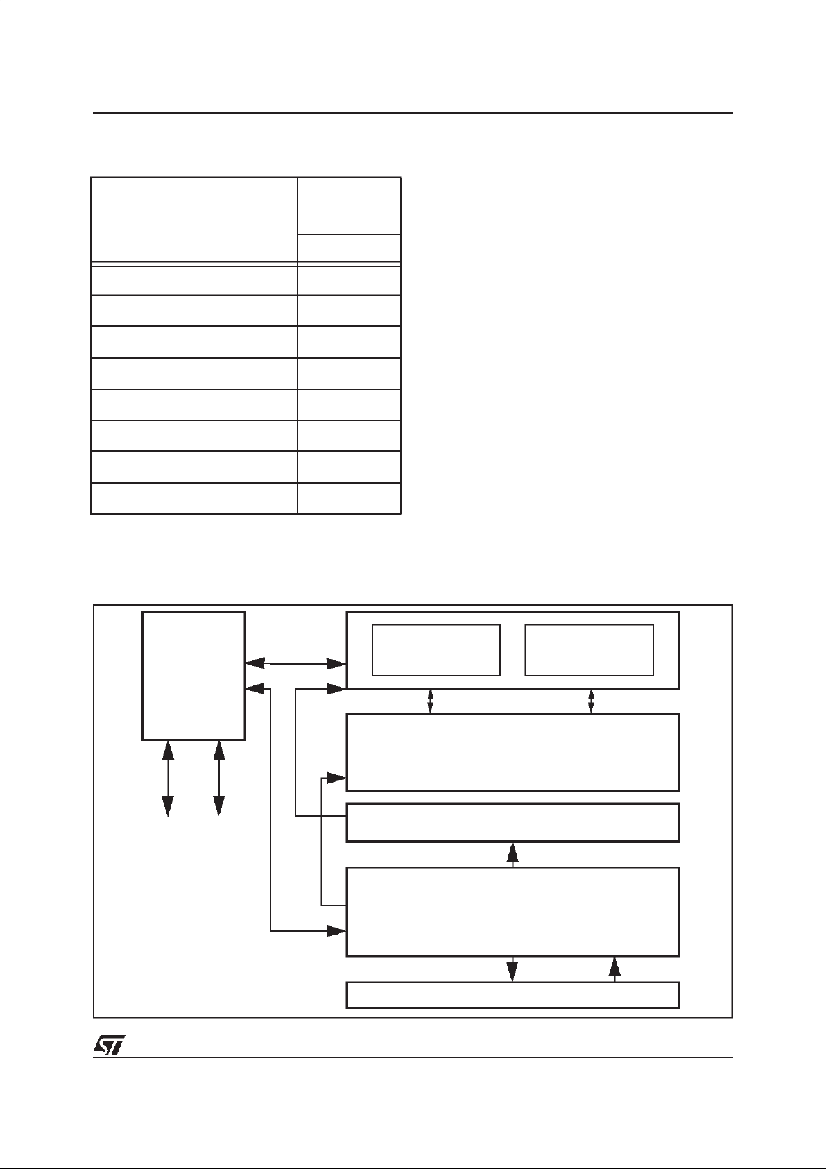
The STLC1510 is a high-speed modem chip that provides the digital portion of a G.992.2 DSL access at a
Central Office (CO) site. It provides downstream and
upstream data transport between an ATM byte
stream and an analog front-end chip using Discrete
Multi-Tone (DMT) Modulation.
The STLC1510 is compliant with ITU-T G.992.2
(G.Lite), G.996.1 (G.Test), G.994.1 (G.Handshake),
G.997.1 (G.Ploam).
Figure 1. Block Diagram
TxClk
TxClav
TxEnb
TxSOC
UTxData[7:0]
TxAddr[4:0]
TxParity
TxBP
RxClk
RxClav
RxEnb
RxSOC
URxData[7:0]
RxAddr[4:0]
RxParity
VDD3_3
VDD2_5
VSS
HPI_Data[7:0]
HPI_Addr [2 :0]
HPI_RWN
HPI_ASN
83
HPI
NIF
FEC
MAP
7
7
14
TAP
TDI
TCK
TDO
EPM
LAMBA Bus
TMS
TRSTN
VDD_PLL
Guard_PLL
EN_D950_EMU
ARM2H P_INT
HPI_CSN
mem
VSS_PL L
ARM_MODE
HPI_CLK
BPU
mem
mem
D950ARM
22
Pmode[1:0]
CMode[1:0]
pgmctrl
Dual
MAC
TGB
8
VCODC
RESETN
GPIO[7:0 ]
D950_CMODE
LinDr_AGC2
LinDr_AGC1
LinDr_Peak
DFE
TxSOUT[1:0]
mem
mem
INF_OUT
REF_OUT
A_SCLK
CK35M
RxSIN[1:0]
REF_CLK
SPI_CLK
SPI_ENB
SPI_DTX
SPI_DRX
November 2000
This is preliminary information ona new product now in development. Details are subject to change without notice.
1/40

STLC1510
2.0 LIST OF MAIN BLOCKS
The STLC1510 G.lite DMT Transceiver is formed by
the following blocks (refer to Figure 1.):
Embedded Processor Module (EPM)
The EPM includes two embedded processor cores:
the ARM7TDMI, a RISC microprocessor, and the
D950, a 16-bit DSP processor. The RISC microprocessor handles the chip control, G.Lite start-up and
showtime control and DSP initialization. It also implements the Framing and Interleaving/Deinterleaving
function required by G.992.2 standard.
Block Processing Unit (BPU)
Computationally intensive digital signal processing
functions are performed in this engine. This engine
utilizes customized DSP architecture that includes
two multiplier/accumulator (MAC).
DigitalFront-End (DFE)
This block provides the interface to an external analog front-end (AFE) device. This block provides decimation, interpolation for the signal sample for the
ADC and DAC on the AFE and signal level monitoring for the analog AGC.
NetworkInterface (NIF)
The NIF is aselectable interface that carries the ATM
signals to and from the STLC1510. This interface
supports one parallel interface (Utopia Level 2) or a
serial data interface. The NIF includes a FIFO to buffer the data between the clock domains of the backend interface and the internal clock.
ForwardError-Correction (FEC)
The Forward Error Correction is done using ReedSolomon Coding. The R-S FEC encoding is performed byte-wise in the transceiver on the transmitted bytes. The two basic parameters that determine
the performance of the code are the code word size,
which consists ofone or more DMT symbols (S), and
the number of redundant check bytes R.
Timing Generation Block(TGB)
The timing generation block generates global clock
and synchronization signals for the STLC1510. It
uses the input clock signals to derive the main internal and output clock signals, as well as all synchronization pulses required to coordinate timing between
the sub-blocks.
Test Access Port (TAP)
This block provides the test access to the STLC1510
using JTAG and BIST techniques.
HPI Interface
A host processor interface is provided to allow the
STLC1510 to be optionally controlled by an external
microcontroller.
3.0 TRANSIENT ENERGY CAPABILITIES
3.1 ESD
ESD (Electronic Discharged) tests have been performed for the Human Body Model (HBM).
The pins of the device are to be able to withstand
minimum 2000V for the HBM.
3.2 Latch-up
The maximum sink or source current from any pin is
limited to 200mA to prevent latch-up.
4.0 ABSOLUTE MAXIMUM RATINGS
The absolute maximum ratings, as specified below,
are those ratings beyond which the device’s lifetime
may be impaired. The meeting of electrical specifications is not implied when the device is subjected to
the absolute limits.
The following table identifies the device’s minimum
and maximum ratings and along with the operatingconditions they define the limits for testing the device
Mapper/De-mapperBlock (MAP)
The Mapper/De-mapper Block (MAP) performs the
bit packing and un-packing and constellation encoder/decoder for a G.992.2 DSL modem. This block
also supports generation of Reverb and medley.
2/40

Table 1. ABSOLUTE MAXIMUM RATINGS
SYMBOL PARAMETER MINIMUM MAXIMUM UNITS
VDD3_3 3.3V Supply voltage w.r.t.VSS (0V) -0.5 4 V
VDD2_5 2.5V Supply voltage w.r.t.VSS (0V) -0.5 3.3 V
STLC1510
T
amb
V
IN,VOUT
V
IN5,VOUT5
I
IN,IOUT
P
D
Ambient temperature -40 85 °C
Voltage at any 3.3V standard input or output -0.5 VDD3_3 + 0.5 V
Voltage at any 5V compatible input or output
1
-0.8 6.3 V
Current at any input or outputs -20 20 mA
Power dissipation 0 0.75 W
Vesd Electrostatic Protection 2000 V
I latchup I/O Latch-up Current V < 0V, V > Vdd 200 mA
<1> -0.8V undershoots and 6.3V overshoots do not last longer than 4nS.
3/40

STLC1510
Figure 2. Ball Map.
STLC1510 Netlist
4/40

Table 2. Pad Description
Signal I/O Pad Type Description BGA
Clock Interface
STLC1510
REF_CLK I 5V TolCMOS input 17.168 MHzor 35.328 MHz reference
clock input.
RESETN I 5V TolCMOS input Hardware reset (active low) E13
D950_CMODE I 5V TolCMOS input ’1’ - Normal operation
’0’ - Reduced REF_CLK frequency in
bypass mode for chip test
PMode_1 I 5V TolCMOS input Power Mode Select G1
PMode_0 I 5V TolCMOS input Power Mode Select H1
CMode_1 I 5V TolCMOS input Clock Mode Select H2
CMode_0 I 5V TolCMOS input Clock Mode Select L1
STLC1511 AFE Interface
A_SCLK I 5V Tol CMOS input ADC/DAC sample frame clock H14
CK35M O 5V Tol3.3V TTL 2mA slew ltd
output
RxSIN_1 I 5V TolCMOS input ADC serial input data L14
RxSIN_0 I 5V TolCMOS input ADC serial input data K14
TxSOUT_1 O 5V Tol3.3V TTL 2mA slew ltd
output
35.328 MHz reference clock output. J14
DAC serial output data F14
1
K13
C13
TxSOUT_0 O 5V Tol3.3V TTL 2mA slew ltd
output
SPI_CLK O 5V Tol 3.3V TTL 2mA slew ltd
output
SPI_ENB O 5V Tol 3.3V TTL 2mA slew ltd
output
SPI_DTX O 5V Tol3.3V TTL 2mA slew ltd
output
SPI_DRX I 5V Tol CMOS input RX STLC1511 input Control Data L13
XTAL_CTRL O 5V Tol 3.3V TTL 2mA slew ltd
output
STLC1512 Line Driver Interface
LinDr_AGC1 O 5V Tol3.3V TTL 2mA slew ltd
output
LinDr_AGC2 O 5V Tol3.3V TTL 2mA slew ltd
output
LinDr_Peak O 5V Tol3.3V TTL 2mA slew ltd
output
DAC serial output data E14
STLC1511 control interface clock M14
TX/RX STLC1511 Enable Control
signal
TX STLC1511 Control Data N14
XTAL output control pin Not on
STLC1511 AGC Gain control 1 D13
STLC1511 AGC Gain control 2 D14
STLC1511 Peakcontrol
2
M13
BGA
C14
5/40

STLC1510
Table 2. Pad Description
Signal I/O Pad Type Description BGA
Test Interface
TCK I 5V TolCMOS input JTAGTest Clock N9
TMS I 5V Tol CMOS input JTAGTest Mode Select N7
TDI I 5V Tol CMOS input JTAGTestData Input P8
TDO O 5V Tol3.3V TTL2mA slew ltd
output
TRSTN I 5V Tol CMOS input dedicated TAPreset (active low) P9
Network Interface (UTOPIA / Serial Clock & Data)
TxClk I/O 5V TolCMOS input/ 5V Tol3.3V
TTL 2mA slew ltd output
TxClav O 5V Tol3.3V TTL2mA slew ltd
output
TxBP O 5V Tol 3.3V TTL 2mA slew ltd
output
TxEnb I 5V Tol.CMOS input Tx Enable. A6
TxSOC I 5V TolCMOS input Tx start of Cell C2
UTxData_7 I 5V TolCMOS input Utopia2 Transmitdata bit 7 G2
UTxData_6 I 5V TolCMOS input Utopia2 Transmitdata bit 6 F2
UTxData_5 I 5V TolCMOS input Utopia2 Transmitdata bit 5 F1
UTxData_4 I 5V TolCMOS input Utopia2 Transmitdata bit 4 E1
UTxData_3 I 5V TolCMOS input Utopia2 Transmitdata bit 3 E2
UTxData_2 I 5V TolCMOS input Utopia2 Transmitdata bit 2 D2
JTAG Test Data Output N8
Input Utopia2 Tx clock or output PSIF
Tx clock.
Tx cell available signal. B5
Tx back pressure signal. B4
A4
UTxData_1 I 5V TolCMOS input Utopia2 Transmitdata bit 1 D1
UTxData_0 I 5V TolCMOS input Utopia2 Transmitdata bit 0; also CDIF
input data
TxAddr_4 I 5V TolCMOS input Utopia2 TransmitAddress B1
TxAddr_3 I 5V TolCMOS input Utopia2 TransmitAddress A1
TxAddr_2 I 5V TolCMOS input Utopia2 TransmitAddress A2
TxAddr_1 I 5V TolCMOS input Utopia2 TransmitAddress A3
TxAddr_0 I 5V TolCMOS input Utopia2 TransmitAddress B2
TxParity I 5V Tol.CMOS input Odd parity bit of the data on
UTxData[7:0].
RxClk I/O 5V TolCMOS input/ 5V Tol3.3V
TTL 2mA slew ltd output
6/40
Input Utopia2 Rxclock or output PSIF
Rx clock.
C1
B3
N6
Table 2. Pad Description
Signal I/O Pad Type Description BGA
STLC1510
RxClav O 5V Tol3.3V TTL 2mA slew ltd
output
RxEnb I 5V Tol.CMOS input Rx Enable. N4
RxSOC O 5V Tol 3.3V TTL 2mA slew ltd
output
URxData_7 O 5V Tol 3.3V TTL 2mA slew ltd
output
URxData_6 O 5V Tol 3.3V TTL 2mA slew ltd
output
URxData_5 O 5V Tol 3.3V TTL 2mA slew ltd
output
URxData_4 O 5V Tol 3.3V TTL 2mA slew ltd
output
URxData_3 O 5V Tol 3.3V TTL 2mA slew ltd
output
URxData_2 O 5V Tol 3.3V TTL 2mA slew ltd
output
URxData_1 O 5V Tol 3.3V TTL 2mA slew ltd
output
URxData_0 O 5V Tol 3.3V TTL 2mA slew ltd
output
Rx cell available signal. P5
Rx start of Cell P4
Utopia2 Receive data bit 7 N3
Utopia2 Receive data bit 6 P3
Utopia2 Receive data bit 5 P2
Utopia2 Receive data bit 4 N2
Utopia2 Receive data bit 3 M2
Utopia2 Receive data bit 2 P1
Utopia2 Receive data bit 1 N1
Utopia2 Receive data bit 0; also CDIF
output data
M1
RxAddr_4 I 5V Tol.CMOS input Utopia2 Receive Address L2
RxAddr_3 I 5V Tol.CMOS input Utopia2 Receive Address K2
RxAddr_2 I 5V Tol.CMOS input Utopia2 Receive Address K1
RxAddr_1 I 5V Tol.CMOS input Utopia2 Receive Address J2
RxAddr_0 I 5V Tol.CMOS input Utopia2 Receive Address J1
RxParity O 5V Tol 3.3V TTL 2mA slew ltd
output
HPI
HPI_Data_7 I/O 5V TolCMOS input/ 5V Tol3.3V
TTL 2mA slew ltd output
HPI_Data_6 I/O 5V TolCMOS input/ 5V Tol3.3V
TTL 2mA slew ltd output
HPI_Data_5 I/O 5V TolCMOS input/ 5V Tol3.3V
TTL 2mA slew ltd output
HPI_Data_4 I/O 5V TolCMOS input/ 5V Tol3.3V
TTL 2mA slew ltd output
HPI_Data_3 I/O 5V TolCMOS input/ 5V Tol3.3V
TTL 2mA slew ltd output
Odd parity bit of the data on
URxData[7:0].
HPI Port Data B14
HPI Port Data A14
HPI Port Data B13
HPI Port Data A13
HPI Port Data B12
N5
7/40

STLC1510
Table 2. Pad Description
Signal I/O Pad Type Description BGA
HPI_Data_2 I/O 5V TolCMOS input/ 5V Tol3.3V
TTL 2mA slew ltd output
HPI_Data_1 I/O 5V TolCMOS input/ 5V Tol3.3V
TTL 2mA slew ltd output
HPI_Data_0 I/O 5V TolCMOS input/ 5V Tol3.3V
TTL 2mA slew ltd output
HPI_Addr_2 I 5V Tol.CMOS input HPI Port Address B7
HPI_Addr_1 I 5V Tol.CMOS input HPI Port Address A7
HPI_Addr_0 I 5V Tol.CMOS input HPI Port Address B8
HPI_CLK I 5V Tol.CMOS input HPI Clock Input B9
HPI_RWN I 5V Tol.CMOS input HPI Port Read/WriteN B10
HPI_CSN I 5V Tol.CMOS input HPI Port Chip Select A8
HPI_ASN I 5V Tol.CMOS input HPI Port Address Strobe Input A10
ARM2HP_INT O 5V Tol3.3V TTL 2mA slew ltd
output
Misc
VCODC I Analog Input VCO control voltage for stand alone
HPI Port Data A12
HPI Port Data A11
HPI Port Data B11
Active-low ARM7 To Host Processor
Interrupt
PLL testing
3
A9
P6
REF_OUT O 5V Tol3.3V TTL 2mA slew ltd
output
INF_OUT O 5V Tol3.3V TTL2mA slew ltd
output
EN_D950_EMU I 5V TolCMOS input EN_D950_EMU=0; D950 core held in
ARM_MODE I 5V Tol CMOS input ARM_MODE=0; Connects external
GPIO_7 I/O 5V TolCMOS input /5V Tol3.3V
TTL 2mA slew ltd output
GPIO_6 I/O 5V TolCMOS input / 5V Tol 3.3V
TTL 2mA slew ltd output
GPIO_5 I/O 5V TolCMOS input / 5V Tol 3.3V
TTL 2mA slew ltd output
PLL REF signal at input to phase
detector
PLL INF signal at input to phase
detector
reset by ARM7, GPIO pin #1,2,3 and
4 are normal mode
EN_D950_EMU=1; D950 core is not
held inreset by ARM7, GPIO pins
#1,2,3 and 4 are dedicated to the
D950 emulator
TAP pins directly to ARM_TAP
ARM_MODE=1; ARM_TAP in daisy
chain configuration after MTAP(i.e.
same as ALPHA configuration)
General Purpose I/O Ports N13
General Purpose I/O Ports P14
General Purpose I/O Ports P13
J13
H13
P7
P10
8/40
Table 2. Pad Description
Signal I/O Pad Type Description BGA
STLC1510
GPIO_4 I/O 5V TolCMOS input / 5V Tol 3.3V
TTL 2mA slew ltd output
GPIO_3 I/O 5V TolCMOS input / 5V Tol 3.3V
TTL 2mA slew ltd output
GPIO_2 I/O 5V TolCMOS input /5V Tol3.3V
TTL 2mA slew ltd output
GPIO_1 I/O 5V TolCMOS input / 5V Tol 3.3V
TTL 2mA slew ltd output
GPIO_0 I/O 5V TolCMOS input / 5V Tol 3.3V
TTL 2mA slew ltd output
Power Supply
VDD3_3_8 P 3.3 volt supply pad 3.3V I/O power supply D3
VDD3_3_7 P 3.3 volt supply pad 3.3V I/O power supply C5
VDD3_3_6 P 3.3 volt supply pad 3.3V I/O power supply C3
VDD3_3_5 P 3.3 volt supply pad 3.3V I/O power supply C4
VDD3_3_4 P 3.3 volt supply pad 3.3V I/O power supply L12
VDD3_3_3 P 3.3 volt supply pad 3.3V I/O power supply M12
VDD3_3_2 P 3.3 volt supply pad 3.3V I/O power supply K12
General Purpose I/O Ports/
D950_IDLE
General Purpose I/O Ports/
D950_SNAP
General Purpose I/O Ports/
D950_INCYCLE
General Purpose I/O Ports/
D950_NERQ
General Purpose I/O Ports/LCLK N10
N12
P12
N11
P11
VDD3_3_1 P 3.3 volt supply pad 3.3V I/O power supply M11
VDD2_5_8 P 2.5 volt supply pad 2.5V ASIC core power supply M3
VDD2_5_7 P 2.5 volt supply pad 2.5V ASIC core power supply L3
VDD2_5_6 P 2.5 volt supply pad 2.5V ASIC core power supply K3
VDD2_5_5 P 2.5 volt supply pad 2.5V ASIC core power supply C10
VDD2_5_4 P 2.5 volt supply pad 2.5V ASIC core power supply C11
VDD2_5_3 P 2.5 volt supply pad 2.5V ASIC core power supply C12
VDD2_5_2 P 2.5 volt supply pad 2.5V ASIC core power supply D12
VDD2_5_1 P 2.5 volt supply pad 2.5V ASIC core power supply M4
VSS_20 P common ground supply pad Ground return for VDD3_3 and
VDD2_5
VSS_19 P common ground supply pad Ground return for VDD3_3 and
VDD2_5
VSS_18 P common ground supply pad Ground return for VDD3_3 and
VDD2_5
VSS_17 P common ground supply pad Ground return for VDD3_3 and
VDD2_5
C9
J3
J12
H12
9/40

STLC1510
Table 2. Pad Description
Signal I/O Pad Type Description BGA
VSS_16 P common ground supply pad Ground return for VDD3_3 and
VDD2_5
VSS_15 P common ground supply pad Ground return for VDD3_3 and
VDD2_5
VSS_14 P common ground supply pad Ground return for VDD3_3 and
VDD2_5
VSS_13 P common ground supply pad Ground return for VDD3_3 and
VDD2_5
VSS_12 P common ground supply pad Ground return for VDD3_3 and
VDD2_5
VSS_11 P common ground supply pad Ground return for VDD3_3 and
VDD2_5
VSS_10 P common ground supply pad Ground return for VDD3_3 and
VDD2_5
VSS_9 P common ground supply pad Ground return for VDD3_3 and
VDD2_5
VSS_8 P common ground supply pad Ground return for VDD3_3 and
VDD2_5
VSS_7 P common ground supply pad Ground return for VDD3_3 and
VDD2_5
VSS_6 P common ground supply pad Ground return for VDD3_3 and
VDD2_5
M6
M5
H3
M7
G3
F3
E3
M9
C6
C7
C8
VSS_5 P common ground supply pad Ground return for VDD3_3 and
M10
VDD2_5
VSS_4 P common ground supply pad Ground return for VDD3_3 and
E12
VDD2_5
VSS_3 P common ground supply pad Ground return for VDD3_3 and
F12
VDD2_5
VSS_2 P common ground supply pad Ground return for VDD3_3 and
M8
VDD2_5
VSS_1 P common ground supply pad Ground return for VDD3_3 and
G12
VDD2_5
VDD_PLL P 2.5 volt supply pad 2.5V supply forPLL G14
VSS_PLL P ground pad Ground return for PLL F13
Guard_PLL P ground pad Ground Voltage reference for PLL G13
<1> 212 MHz in PLL bypass mode
<2> This pad is configured as a pseudo open drain connection and can only pull the output low, or go high impedance
<3> Add pullup to this pin on board. This pad is configured as a pseudo open drain connection and can only pull the output low, or go high
impedance
10/40

STLC1510
5.0 MAIN BLOCK DESCRIPTION
The following sections describe the sequence of
functions performed by the chip
5.1 Network Interface and Controller (NIF)
The Network Interface and Controller block (NIF) is
responsible for transferring data between the
STLC1510 and the ATM network. The NIF has two
interfaces to the backplane: an 8-bit Utopia Level 2
Physical Interface (U2PHY) and a clock and data serial interface (CDIF). It communicates with the rest of
the STLC1510 via the LambaBus. Figure 3. shows a
functional/data path block diagram of the NIF (this diagram does not include all glue logic between the
major functional blocks). 37 external pins are required for the U2PHY and CDIF interfaces (19 for the
Tx direction, 18 for Rx). Pins are shared between the
two interfaces, as they will not both be active at the
same time.
5.1.1 Features
■
Utopia Level 2 8-bit parallel interface.
■ Up to 9 ATM cells (477 bytes) of rate adaptation
buffering for the Utopia Level 2 TX interface.
The amount of buffering is programmable via a
memory-mapped register.
■
Up to 2 ATM cells (106 bytes) of rate adaptation
buffering for the Utopia Level 2 RX interface.
The amount of buffering is programmable via a
memory-mapped register.
■
ATM Transconvergance (TC) layer cell
processor with 16-bit data path: performs
scrambling/descrambling, HEC calculation, cell
delineation with error detection (no error
correction) and cell rate decoupling by idle cell
insertion/detection.
■ Clock and Data serial interface.
■ Implemented as a hardware module on the
Lamba bus with an 8-bit data interface and 16bit control interface.
■ 4 ATM cells (212 bytes) of rate adaptation
buffering in each direction (TX and RX) for
interfacing to the Lamba bus.
■
Pads partial or runt cells (ATM cells of length
less than 53 bytes) to 53 bytes in the TX
direction to prevent loss of synchronization at
theCPE.
5.1.2 External Interface (Pins)
The STLC1510 connects to the ATM network via 37
external pins. These are illustrated in Figure 3. Note
that the pins TxClk and RxClk are bidirectional and,
along with UTxData[0] and URxData[0], are shared
between the CDIF and U2PHY
5.1.3 Clock and data serial Interface (CDIF)
The STLC1510 can communicate serially to an ATM
network through the CDIF. Two serial data lines,one
for the Tx path (CO to CPE), the other for the Rx path
(CPE to CO), and two respective clocks realize the
exchange of information and control signals between
the STLC1510 and the network.
The CDIF of the STLC1510 has the following attributes:
■
Synchronizes to the ATM network.
■
Provides Tx and Rx clocks to the ATM network.
Transfers data between the ATM network and the
STLC1510’s Lamba Bus
■
Accepts idle ATM cells inserted by the ATM
network in the Tx direction. These idle cells are
used by the ATM network to adapt to the clock
provided to it by the STLC1510.
■
Generates clock gapping in the Tx direction.
This serves two purposes: it is a flow control
mechanism to theATM network chip, andit can
be used for the byte alignment. In the bytealignment role, a clockgap longer thana pre-set
threshold indicates that the most significant bit
of a byte should be transmitted on the next
rising clock edge. This is useful for aligning data
bytes to the overhead bits inserted by the
STLC1510. In the flow control role, incoming
data is not sampled when the clock is off. The
threshold used to distinguish between byte
alignment and flow control clock gapping is
software programmable and has a range offrom
0 to 65535 clock cycles (a 16 bit register stores
the value).
■
Generates clock gapping in the Rx direction.
This serves asa flow-control mechanism; when
there is no data available for transmission to the
backplane, the clock is shutoff, ensuring that no
invalid data bits are sampled by the backplane.
11/40

STLC1510
Figure 3. NIF Off-Chip Signals
TxC lk
UTxData[0]
UTxData[7:1]
TxAddr[4:0]
TxParity
TxEnb
TxSOC
TxClav
TxBP
CDIF
TX
URxData[0]
8
5
U2PHY
TX
URxData[7:1]
RxClk
RxEnb
RxSOC
RxAddr[4:0]
RxClav
RxParity
8
5
CDIF
RX
U2PHY
RX
The following tasks are performed by the ATM network (in accordance with ITU-T Recommendation
I.432.1), and therefore do not have to be implemented in the STLC1510 when using the CDIF:
■
HCS generation (Tx).
■
Payload scrambling (Tx).
■
Optionally, enables clear channel mode, in
which HCS generation and payload scrambling
are disabled (Tx).
■
HCS cell delineation (Rx).
■ Payload descrambling (Rx).
■
Idle cell filtering (Rx).
■
Header error detection to recover valid ATM
cells (header correction is not implemented)
(Rx).
■
Optionally, enables clear channel mode, in
which every 53 x 8 = 424 bits are collected by
the receiver and sent to the backplane (Rx).
5.1.4 UTOPIA Level 2 Interface and Controller
The Universal Test and Operations Physical Interface forATM (UTOPIA) provides a standard that links
ATM layer orvarious management entities with a variety of physical (PHY) layers.
The UTOPIA IF has the following features:
■
provides clock decoupling mechanism.
■ throttles data flow from the ATM layer.
■
indicates to the ATM layer when the modem is
ready to receive data.
■ signals tothe ATM layer the presence of valid
data for transmission.
■
Recognizes the address when the modem is
selected for communication.
■ Supports octet-level and/or cell-level
handshaking.
■
UTOPIA Level 2 supports a multi-PHY
operation for up to n PHY devices where,
■
n=< 8 at ATM layers intended for 155 Mbps;
12/40

■
n=< 4 at ATM layers intended for 622 Mbps.
■ This interface is subdivided into two parts: the
Transmit Interface (TxIF) and the Receive
Interface (RxIF).
■ Both the TxIF and RxIF are controlled by the
ATM layer.
■
The ATMlayerprovides aninterface clock tothe
PHY layer for synchronizing all interface
transfers.
■
The PHY layer will incorporate rate-matching
buffers.
■
Transmit data is transferred from the ATM layer
to the PHY layer as follows: first, the PHY layer
indicates itcan accept data, then the ATM layer
drives data onto the data bus and asserts the
TxEnb.
■ The data flow is controlled by the PHY layer.
For a complete definition of TxIF signals and RxIF
signals please consult the UTOPIA Level 1 and UTOPIA Level 2 documents released by The ATM Forum
Technical Committee.
There is an additional signal added to the Utopia Interface in the TX direction: Back Pressure (TxBP).
This signal alerts the backplane when a software programmable depth has been reached in theTX Utopia
FIFO, while still allowing more data (up to the 10 cells
maximum) to be accepted by the FIFO.
5.1.5 ATM Transport Convergence (TC) Layer
Processor
The Cell TC block has the following attributes:
■
Idle cells inserted in the Tx direction for cell rate
de-coupling are discarded.
■
HEC bytes are generated inthe Tx direction as
described in ITU-T Recommendation I.432,
including the recommended modulo-2 addition
(XOR) of the pattern binary 01010101 to the
HEC bits.
■ Scrambling of the cell payload is used in the
transmit direction to improve the security and
robustness of the HEC cell delineation
mechanism. The cell payload isdescrambled by
the Cell TC block of an ATU receiver.
■
When interfacing ATM bytes to the bearer
channel, the most significant bit (msb) is sent
STLC1510
first.
■ Cell delineation isperformed usinga coding law
checking the HEC field in the cell header
according to the algorithm described in ITU-T
Recommendation I.432.
■
Error detection is performed asdefined in ITU-T
Recommendation I.432 with the exception that
any HEC error is considered a multiple-bit error.
Therefore, HEC error correction is not
performed.
■ The ATU-C transmitter preserves V-C and T-R
interface byte boundaries (explicitly present or
implied by ATM cell boundaries) at the U-C
interface.
■
Interfaces to the Lamba bus.
5.2 FIFO
The STLC1510 incorporates 4 FIFO buffers for rate
decoupling:
■
Utopia TX FIFO (8 bit input from the Utopia TX
interface, 16 bit output to the ATM-TC cell
processor): 243 words X 16 bits/word = 486
bytes >= 9 ATM cells @ 53 bytes/cell
■ Utopia RX FIFO (16 bit input from the ATM-TC
cell processor, 8 bit output to the Utopia RX
interface): 54 words X16 bits/word = 108 bytes
>= 2 ATM cells @ 53 bytes/cell
■
Lamba TX FIFO (16 bit input from the ATM-TC
cell processor, 8 bit output to the Lamba Bus):
106 words X 16 bits/word =212 bytes >= 4 ATM
cells @ 53 bytes/cell
■ Lamba RX FIFO (8 bit input from the Lamba
Bus, 16 bit output to the ATM-TC cell
processor): 106 words X 16 bits/word = 212
bytes >= 4 ATM cells @ 53 bytes/cell
■
All the FIFO’s share the following features:
■
Perform 8-bit to 16-bit word conversion or 16-bit
to 8-bit word conversion, with storage
implemented as 16-bit wide dual port RAMs.
■
Flags indicating when the FIFO is full, almost
full, empty, almost empty and half empty. (The
FIFO depths for the almost full and almost
empty flags are hard-wired).
■ Diagnostic input and an error flag.
■
The Utopia Tx FIFO has the following additional
attributes:
13/40

STLC1510
■
Software programmable generation of the flag
TX_CLAV (CeLl AVailable, TX direction) via
registers. This translates to the FIFO having a
software programmable depth.
■ Software programmable generation of the flag
TX_BP (Back Pressure, TX direction) via
registers. This allows the FIFO to throttle
incoming data flow, while still accepting data
that was already en route when the flag was
asserted.
The Utopia Rx FIFO has the following additional attributes:
■
Software programmable generation of the flag
RX_CLAV (CeLl AVailable, RX direction) via
registers. This translates to the FIFO having a
software programmable depth.
5.3 Reed Solomon Forward Error Correction
(RS-FEC)
Forward error correction is provided with byte-wise
Reed Solomon (RS) Encoding andDecodingin a 256
element Galois Field.
5.3.1 Parameters
The following parameter values for and are
SR
supported:
■
■
,,,=
R04816
S 124816,,,,=
Furthermore
■ is integer,
RS⁄
■
the combination and is
S1> D1
=
allowed, while not required.
■ byte wise coding over ,
■
and hence .
N
FEC
The Reed-Solomon Code Word length is , and
its value results from theselection of and , and
the number of data bytes per Data Frame, whereby for downstream, or
B2…48…144=
B1…16…60=
for upstream. The RS Data Word
GF 256()
255≤
B
N
FEC
SR
length is
K
FEC
+()⋅=
SB1
and theRS Code Word length is
N
FEC
The code word istransmitted over DMT symbols,
KR+=
S
and hence the number of bytes per Data Frame is
N
B’
FEC
-------------- - B1+
S
The Galois Field primitive element is defined by
R
--- -+==
S
α
the zero of the primitive polynomial
px() x8x4x3x21++++=
The Reed-Solomon generator polynomial is
–
R1
k
=
Gx() x α
k0
+
()
∑
=
The RS encoder does not introduce latency. RS decoding has a latency of at least , whereby the up-
N
per bound of the latency is given by the actual
decoder implementation.
The transmitter and receiver provide synchronization
of the RS Code Words.
5.4 Bit Mapper/Demapper Module (MAP)
5.4.1 Features
■
G.992.2 Compliant constellation encoder, up to
15 bits per sub-carrier capability.
■ Support for 1-bit per sub-carrier modulation
(BAM) and idle sub-carriers.
■
Constellation encoder, Q1.15 complex fixed
point output.
■
Bit unpacking and packing from/to 256-byte
data frame.
■ Support for pilot tone insertion.
■
Support for REVERB, SEGUE and MEDLEY
generation.
■ Support for random 4-QAM generation.
■
No trellis coding.
■
Implemented as a peripheral device.
14/40

5.4.2 Mapper Description
The mapper realizes the bit extraction and constellation encoding functions specified in G.922.2 (§ 7.8.1
and § 7.8.2 respectively); it is mainly intended to accelerate the main CPU in these bit manipulation operations.
The mapper consists of:
■ A Bit Unpack unit, extracting a variable length
bit string from the frame RAM
■
A Constellation Encoder, converting the bits to
a constellation point
■
Pseudo -random sequence generators PRBS,
& MAPPRG.
5.4.3 Demapper Description
The demapper consists of:
■
A Constellation Decoder, converting the input
constellation point to bits.
■
A Bit Pack unit, inserting the variable length bit
string into the frame RAM.
STLC1510
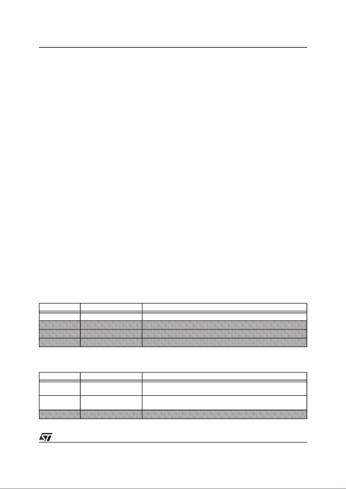
5.5 Embedded Processor Core - Functional
Description
The Embedded Processor Core consists of two programmable cores; the ARM7TDMI 32-bit microprocessor and the D950 16-bit DSP, their associated
peripherals/memory, a DPCOMM (Dual-Port Communications) for messaging, and a Bridge/Arbiter/
Decode (BAD) block. A block diagram of the EPM is
shown below.
There are two buses locally used by the ARM7 core
which are collectively known as the Advanced Microcontroller Bus Architecture (AMBA):
■
Advanced System Bus (ASB)
■ Advanced Peripheral Bus (APB) connected to
the ASB via an APB Bridge
The LAMBA Bus, a subset of the AMBA bus specification, connects all the blocks in the data pump portion of the STLC1510.
Figure 4. EPM and LAMBA Bus Block Diagram
EPM
ASB can extend to the APB,
X Bus , Y Bus, P Bus and
LAMBA Bus.
X Bus can extend to LAMB A
Bus.
APB
Tmr
ASB
Mem
APB
Bridge
Dec
HPI
I/F
Off Chip
ARM7
CORE
EMU TAP
Int
Cntl
Boot
ROM
Bridge/
Arbiter/
Decod e
DPCOMM
X BUS
Y BUS
P BUS
Xmem
Ymem
Pmem
LAMBA BUS
16
Int
Ctrl
Tmr
Dec
Dec
D950
COR E
EMU TAP
15/40

STLC1510
5.5.1 EPM Attributes
■ It provides access to internal registers for
control and monitoring of the various hardware
blocks.
■ Provides control to perform Software (SW)
download into the EPM and BPU memories as
part of the power up sequence.
■ Provides interrupt and exception handling for
various macro blocks.
■
Software on the EPM preforms several DSP
functions that are not implemented in the BPU
during Start-up, fast re-train or Show Time.
■
Address space is large enough to address the
internal registers, on-chip and some off-chip
memories
■
Provides debugging access through a JTAG
interface, for SW running on the processor.
■
Provides a dual port RAM to pass messages
between the D950 and ARM7 cores.
■ Supports an external Host Processor Interface
to pass messages to/from the ARM7
■
Both cores have embedded emulator blocks for
debug
5.5.2 ARM7TDMI MCU Core
The ARM7TDMI is a member of the Advanced RISC
Machines (ARM) family of general purpose 32-bit microprocessors. The architecture is based on the Reduced Instruction Set Computer (RISC) principle
which results in high instruction throughput and fast
real-time interrupt response.
Pipelining is employed so that all parts of the processing and memory systems can operate continuously. While one instruction is being executed, the
next is being decoded while the next is being fetched
from memory.
Attributes:
■
32-bit register bank
■
32-bit ALU
■ 32-bit shifter
■ 32-bit addressing
■
32x8 DSP multiplier
■
”Thumb” architectural extension which allows
generation of more memory efficient code
■
Peripherals include decoders, timer and
interrupt controller
5.6 D950 DSP Core
The D950 core is a 16-bit DSP based on the Harvard
architecture with three bidirectional 16-bit buses, two
for data and one for instruction. Each of these buses
is dedicated to a unidirectional 16-bit address bus
(XA/YA/IA).
The core is composed of three main units, a Data
Calculation Unit (DCU), an Address Calculation Unit
(ACU) and a Program Control Unit (PCU).
Attributes
■
Data Calculation Unit
■
Address Calculation Unit
■
Program Control Unit
■ 16x16 single cycle MAC
■
fast and flexible buses
The D950 top level consists of a D950 core, I mem,
X mem1 (8 bit), X mem2 (16 bit), Y mem, Timer, Emulator, Interrupt Controller and TAP peripherals.
5.6.1 BAD - Bridge, Arbiter, Decoder
The Bridge/Arbiter/Decoder (BAD) block controls the
data traffic among the ARM7, the D950 and the data
pump. It provides decoding circuitry, LAMBA bus arbitration and isolation buffers.
5.6.2 DPCOMM - Dual Port RAM Messaging
between ARM and D950
A Dual Port SRAM (1024x16) plus control registers,
is connected between the APB bus of the ARM7 and
the X bus of the D950. It is used as a mailbox to pass
data between the ARM and the D950 DSP.
5.7 Host Processor Interface (HPI)
■
The HPI resides on the APB bus of the ARM7.
The chip select for the HPI is generated by the
APB Bridge. Since the HPI resides on the APB,
it is treated as a 16 bit entity. This means that
APB Address 0isignored and allHPIaddresses
are on 16 bit boundaries. i.e. incremental
address location are h0000 h0002 h0004 etc...
■
The HPI is dual port SRAM based with control
that generates an interrupt when a message
wants to be passed. The DPSRAM is
implemented on-chip.
■
External to the ASIC, the pins of this interface
are 8 bidirectional data pins, 3 input address
pins, 1 input Read/Writen pin,1 Address Strobe,
1 clock, 1 input chip select pin and 1 output
interrupt pin.
16/40
■
A status register, an index register (for the Host
Processor), an interrupt mask register, and a
message buffer are required for both input and
output transactions.
■ The Input Status Register (ISR) is set by the
Host Processor by writing h01 and cleared by
writing h00 to the location. It is cleared by ARM
by writing anything to it.
■
The OutputStatus Registers (OSR)isset by the
ARM by writing h01 and cleared by writing h00.
It is cleared by the Host Processor by writing
anything to it.
■
The Input and Output Index Registers (IIR &
OIR respectively) are reset to their starting
value by writing h00 to their respective
addresses. They can also be cleared by the
Host Processor by writing anything to them.
■
The Input Interrupt Mask Register (IIM) resets to
h00, causing the Mask to be set (active low).
This means that before the ARM can receive
message ready interrupts from the Host
Processor, this register must be written with
STLC1510
h0001 (by ARM) to unmask the interrupt.
■ The Output Interrupt Mask Register (OIM)
resets toh00, causing the Mask to beset (active
low).This meansthat before theHostProcessor
can receive message ready interrupts from the
ARM, this register must be written with h01 (by
the Host Processor) to unmask the interrupt.
■ The Input and Output Message buffers are each
256 bytes long and 1 byte wide (an overflow in
the index register will not write to the other
message buffer, but will start to overwrite the
current message buffer).
■
Addressing of the Input and Output Message
Buffers by the Host Processor is implemented
indirectly via the Input and Output Index
Registers.
■
An external interrupt signal is generated when
the output status register isset bytheARM7. An
ARM7 interrupt signal is generated when the
input status register is set by the Host
Processor.
Figure 5. HPI Block Diagram
To/From
ARM
BCLK
BRESn
PSEL_HPI
PWR ITE
PENABL E
PADDR[10:1]
PD_W[7:0]
PD _R [15 :0]
H PI2 A RM_INT
InputInt M ask
O utput S tatus R e g
256 Bytes
Output
Message
S
L
A
A
P
V
B
E
Read/Write
Buffe r
Read
256 Bytes
InputMessage
Output Int M ask
Output IndexReg
Input IndexReg
Input StatusReg
Read
Read/Write
Buffer
H
P
To/From
HPI
ARM 2HP_ INT
HPI_CSN
HPI_RWN
HPI_ASN
C
HPI_ADDR[2:0]
N
HPI_DATA_IN[7:0]
T
R
HPI_DATA_OUT[7:0]
L
HPI_DATA_OEN
HPI_CLK
17/40
STLC1510
5.7.1 Send Message from Host Processor to
ARM
■
Read Input Status Register. Ifh01, the ARM has
not read out the last message. If h00, the ARM
has read the last message and the Input
Message Buffer is available for use.
■
Clear Input Index Reg by writing any value to its
address (b’100).
■
Write message into Input Message Buffer by
consecutively writing to its address (b’111). Each
write will cause the Input Index Register to
increment by 1 and access another byte location.
■
Write h01 to Input Status Register (address
b’011) to interrupt the ARM
5.7.2 Receive Message from ARM by Host
Processor
After receiving interrupt from ARM:
■
Clear Output Index Register (address b’001) by
writing any value.
■ Read message from Output Message Buffer by
consecutively reading from its address (b’110).
Each read will cause the Output Index Register to
increment by 1 and access another byte location.
■ Clear theOutput Status Reg (address b’000) by
writing any value (the ARM can clear the OSR
by writing 0 to it).
■ Send Message from ARM to Host Processor
■
Read Output Status Register. If h0001, the HP
has not read out the last message. Ifh0000, the
HP has read the last message and the Output
Message Buffer is available for use.
■
Write message into Output Message Buffer.
This buffer is directly addressable by the ARM.
■
Write h0001 to Output Status Register to
interrupt the HP
5.7.3 Receive Message from Host Processor
by ARM
After receiving interrupt from HP:
■ Read message from Input Message Buffer.This
buffer is directly addressable by the ARM.
■
Clear the InputStatus Reg by writing h0001 to its
address (the HP can clear the ISR by writing0 to it).
Table 3. Signal List
Name I/O
BRESn I Internal APB Active low master RESET
BCLK I Internal APB ASB clock
PSEL_HPI I Internal APB Active high block select from APB
PADDR[10:1] I Internal APB APB address [11:1]
PD_W[7:0] I Internal APB APB write data
PD_R[15:0] O Internal APB APB read data
PWRITE I Internal APB APB Write - Active high, Read - Active low
PENABLE I Internal APB APB enable signal for timing
HP2ARM_INT O Internal APB Interrupt from Host Processor to ARM
HPI_CLK I External HP Host Processor bus clock
HPI_CSN I External HP Active low select from Host Processor
HPI_ASN I External HP Address Strobe from Host Processor
HPI_RWN I External HP HP Read - Active high, Write - Active low
HPI_ADDR[2:0] I External HP Host Processor address
HPI_DATA_IN [7:0] I External HP Host Processor data in
HPI_DATA_OUT [7:0] O External HP Host Processor data out
HPI_DATA_OEN O External HP Host Processor data output enable
ARM2HP_INT O External HP Interrupt from ARM to Host Processor
Internal/
External
I/F Description
18/40
STLC1510
Table 4. HPI Memory Map 5.8 Block Processing Unit (BPU) Functional
Description
HPI Reg
Output Status Reg 000
Output Index Reg 001
Output Mask Reg 010
Input Status Reg 011
Input Index Reg 100
Input Mask Reg 101
Output Message Buffer 110
Input Message Buffer 111
Figure 6. BPU Core Block Diagram
Host
Processor
Addr
BIN
5.8.1 Block Processing Unit - Core
The BPU is a programmable Digital Signal Processor
responsible for the bulk of the high rate signal processing required in the modem. This processor utilizes a dual multiply accumulate Arithmetic Unit (AU)
and Very Long Instruction Word (VLIW) format to
achieve high processing efficiencies.
The BPU is designed to perform the following functions:
■
Finite Impulse Filters (FIR)
■ (Infinite Impulse Response) IIR
■
FFT/IFFT
■
Compression/decompression for FFT/IFFT
■
FDEQ
■
Tx Gain
■ SNR calculation - recursive average
■
add/remove cyclic prefix
■ Slicer
■
Auto Correlation
■ FDEQ update
■
Digital AGC
MCU/DFE
DATA
MEMORY
INTERFACE
INTERFACE
DFE
STLC1510 BUS INTERFACE
DATA MEM CDATA MEM
X
(XDM)(C
PORT
X
DM
)
C
ARITHMETIC UNIT (AU)
CONTROL
AU
ADDRESS CALCULATION UNIT (ACU)
PROGRAM CONTROL UNIT (PCU)
CONTROL
AU
PROGRAM
MEMORY
ADDRESS
PROGRAM MEMORY
PORT
PROGRAM
MEMORY
DATA
19/40

STLC1510
5.9 Digital Front End (DFE)
The Digital Front End (DFE) block contains dedicated
hardware to map signals between the analog interface (AFE) and the BPU.
The DFE block has the following features:
■ It performs part of the sampling rate conversion
between the AFE sampling rate and the 2x
in CPE mode. This consists of a digital phase
interpolator and a digitalΣ∆ D/A convertor
■
Two loopback modes are provided in this block.
■
Various bypass modes are provided to allow
observation and isolation of any block in the
DFE for test purposes.
■
Interface to the LAMBA Bus.
symbol rate of the BPU.
■ It provides the necessary digital hardware to
implement ananalog-based AGC.
■
It provides the necessary buffering to provide
DMT symbol alignment within the BPU.
■
It provides the facilities to allow timing recovery
5.9.1 Application Description
Figure 7. shows the application of the various DFE
components when used in a CO (network) and CPE
(remote) applications.
Figure 7. DFE Application Diagram
STLC1510 (CO) STLC1520 (CPE)
PIF
PD
Dly
RSM
DFE
DFE
ADC
DAC
~4.416 MHz
CIC
Filter
~4.416 M H z
CIC
Filte r
Σ∆
optional
r
o
2.208 M Hz
CIC
Filter
2.208 M Hz
Interp
CSD
FIR
1.104 M Hz
IIR
FIFO
552 kHz
~2.208 M H z
t
a
l
o
p
r
e
t
n
I
e
s
a
~2.208M Hz
h
P
BPU
2.208 M Hz
IIR
FIFO
552 kH z
2.208 M Hz
Interpolating
CSD FIR
CIC
Filter
552 kHz
4.416MHz
DAC
Analog
4.416 MH z
Domain
ADC
RSM
2.208 M Hz
BPU
552 kHz
5.9.2 Interface Description
The registers accessible by the EPM are:
■
Decimator oversampling ratio
■ Decimator order.
■
Various loopback and bypass modes.
■
Number of bits transferred to the Aloha ASIC
DAC.
■
AFE control registers.
■ ADC clip counter.
■
RSM parameters such as time constant, peak
detector thresholds, peak detector modes,
20/40
integrator initialization, and detector outputs.
■ IIR coefficients.
■
Predictor IIR filter coefficients.
■ Frame synchronization buffer length
■
Timing recovery (crystal) control word.
■
Timing recoveryΣ∆ dither level selection.
■
CO/CPE mode selection.
■
Phase interpolator parameters such as alpha,
frequency error and frequency error gain.
■
CO peak detector parameters such as set-up
and hold delays, threshold, and slew rate.
5.10Timing Generation Block (TGB)
The timing and reset generation block generates the
device’s global clock and synchronization signals.
It uses the input clock signal (35.328 or 17.664 MHz)
to derive the main internal clock signals, as well as all
synchronization pulses required to coordinate timing
between the sub-blocks. It also synchronizes the external RESETN with the internal ASIC clock.
The PLL input source, and PLL bypass signals are decoded from the PMode[1:0] pins. The CMode[1:0] pins
are configured toalwaysprovidean 8.8 MHz inputto the
PLL when the PLL is not in bypass mode. Thus adivide
by 2 or 4 will be selected to divide down the 17 or 35
MHz input clock references to 8.8 MHz. When the PLL
is to be bypassed, it is powered down, and the input reference is used to bypass the PLL output.
The CK35M signals are generated by dividing down
the internal ASIC clock. A 3 bit memory mapped register is used to adjust the reset phase ofthe divide by
6 generator. This gives software control of the phase
of theCK35M signal which interfaces to the AFE device. There is also a programmable ”one shot” mode
which is used to reset the phase of the CK35M in the
event the interface cannot synchronously meet the
timing requirements.
The NIFTX_CLK and NIFRX_CLK are generated
when the NIF is in clock and data mode, i.e. not utopia mode.
5.10.1RESET Structure
The RESET structure for the STLC1510 has the following requirements/attributes:
STLC1510
■
Requires off-chip power supervisor to supply
10ms power-on reset (may also require push
button reset for test) and 5ms TRSTN (TAP
reset).
■
Reset initialization will begin when RESETN is
de-asserted by the off-chip power supervisor.
After 2 rising edges of 4.4MHz clock,
ASIC_RESETn is de-asserted and the
STLC1510 (minus the BPUand D950 cores) will
come out of reset. The ARM7 will follow its boot
procedure which at some point, will download
program code to the BPU and D950 cores then
release them individually from reset.
5.11Test Access Port Functional Description
The IEEE 1149.1 compliant Test Access Port (TAP)
serves three purposes:
■ TAP interface for both ASIC and board level
testing
■
RAMBIST interface for testing the embedded
memories during ASIC level test.
■
General Purpose I/O port for general and
miscellaneous control and monitoring.
In addition to these functions, there are two sets of
mode pins,
PMODE[1:0
], and
are used to put the STLC1510 into various modes.
The definition of these modes are given below, where
the shaded rows indicate special modes not to be
used in normal operations.
CMODE[1:0]
which
Table 5. Power Mode Pin Definition
PMODE[1:0] Mode State Description
00 Power Down Mode 0 Nothing is powered down.
01 Power Down Mode 1 ARM7 is powered down.
10 Power Down Mode 2 D950 is powered down.
11 Power Down Mode 3 BPU processor is powered down
Table 6. Clock Mode Pin Definition
CMODE[1:0] Mode State Description
00 Div2 Master clock is REFCLK divided by 2 and then multiplied by24. The
input REFCLK should be 17.664 MHz
01 Normal Master clock is REFCLK divided by 4 and then multiplied by 24. The
input REFCLK should be 35.328 MHz
1X Bypass Master clock is REFCLK
21/40
STLC1510
5.11.1DFT Interfaces
The STLC1510 incorporates certain features (Design
for Testability, DFT) to improve thecoverage of the final production test. Certain pins are dedicated to this
features, and should not be used duringnormal operation. The Test Interface pins need to be connected
as follows:
Signal BGA Connected to
TCK N9 Pull-Up
TMS N7 Pull-Up
TDI P8 Pull-Up
TDO N8 open
TRSTN P9 See “RESET Structure” on
page 21.
5.11.2General Purpose I/O (GPIO) Interface
The STLC1510 has a 8-bit General Purpose I/O port
Figure 8. GPIO Interface Block Diagram
to allow low speed control and monitoring of external
signals via the LAMBA bus. The block diagram for
this interface is shown in Figure 8.
The GPIO has the following attributes:
■
There are 8 GPIO pins.
■
Each pin can be individually set to one of 4
modes:
• Input mode: Input signals will be sampled with LAMBA bus clock and stored in
GPIO_in register.
• Output mode: The GPIO pin is driven
with the state in theGPIO_out register.
• Interrupt mode: The
GPIO_int
register
is set when there is a negative transition
detected on its corresponding GPIO pin.
The logic levelof each interrupt pin will as
well be stored in theGPIO_in register. An
interrupt condition on any of the GPIO
pins will result in an interrupt to the D950.
• Dedicated mode. The GPIO pin is configured to be its second function according to the Table below If the pin does not
have a second function, it will be configured as an input pin.
■
There isno external clock for the GPIOinterface
and as such no timing defined.
Lamba
Bus
GPIO[7:0]
GPIO_in GPIO_outGPIO_int
GPIO _state
Lamba BusInterface (LBI)
22/40
STLC1510
5.12Processor Emulation
There are three programmable processors on the
LAVA ASIC: an ARM microprocessor, a D950 Digital
Signal Processor, and a custom DSP engine (BPU).
All these are capable of JTAG based emulation with
the following attributes:
■
Stop on breakpoint.
■ Single step
■ Full register R/W.
■
Program modification and resume.
6.0 ELECTRICAL CHARACTERISTICS
This device shall meet the functional requirements
detailed herein when operated over the specified timing, electrical, and temperature range.
7.0 OPERATING RANGES
The operating ranges shall be in accordance with the
following table.
Table 7. Operating Ranges
SYMBOL PARAMETER MIN. NOM. MAX. UNITS
VDD3_3 CMOS 3.3v I/OSupply voltage 3.0 3.3 3.6 V
VDD2_5 CMOS 2.5v Core Supply voltage 2.25 2.5 2.75 V
I
DD3
I
DDS3
I
DD2
I
DDS2
T
A
T
J
<1> Assuming no air flow and a package thermal resistance of 30×C/watt
CMOS 3.3v I/O Supply current 11 mA
CMOS 3.3v I/O Static supply current TBD mA
CMOS 2.5v Core Supply current 240 mA
CMOS 2.5v Core Static supply current TBD mA
Ambient temperature under bias
1
-40 25 85 ×C
Operating junction temperature -40 25 105 ×C
7.1 DC Characteristics The following table identifies the general DC charac-
teristics for input and output pins.
Table 8. General Interface Electrical Characteristics
SYMBOL PARAMETER Conditions Min Typ Max Unit
V
il
V
ih
V
ol
V
oh
I
il
I
ih
I
oz
I
pu
I
pd
R
up
Rpd Equivalent pull-down resistance Vi = VDD2_5 50 k
<1> Takes into account 0.075*Vdd voltage drop in both supply lines.
<2> The leakage currents are generally very small, < 1nA. The value given here, i µA, is a maximum that can occur after an Electrostatic
Stress on the pin.
Low level i/p voltage 0.8 V
High level i/p voltage 2.0 V
Low level o/p voltage
High level o/p voltage
1
a
Low Level Input Current without pull-up
2
device
High Level Input Current without pull-
down device
b
Tri-state Output leakage without pull
up/down device
b
Iol= 2mA 0.4 V
Ioh= 2mA 2.4 V
Vi=0V 1.0 µA
Vi=VD3_3
Vi=VDD5
Vo=0Vor
2.0
4.0
µA
µA
1.0 µA
VDD3_3
Pullup current Vi= 0V -50 µA
Pulldown current Vi= VDD5 100 µA
Equivalent pull-up resistance Vi=0V 50 k
Ω
Ω
23/40
STLC1510
7.2 AC Characteristics
7.2.1 AFE Interface Timing
Figure 9. AFE Data Interface Timing (TTL)
CK 35M
Tx S OU T [1 :0 ]
tacc
tse
tho
RxSIN[1:0]
tse
tho
AS_CLK
Table 9. AFE Data Interface Timing
Pin Name Parameter Min. Max. Reference Pin
TxSOUT[1:0] tacc 0 10ns w.r.t. rising CK35M
TxSIN[1:0] tse 5ns w.r.t. rising CK35M
TxSIN[1:0] tho 5ns w.r.t rising CK35M
AS_CLK tse 5ns w.r.t. rising CK35M
AS_CLK tho 5ns w.r.trising CK35M
24/40
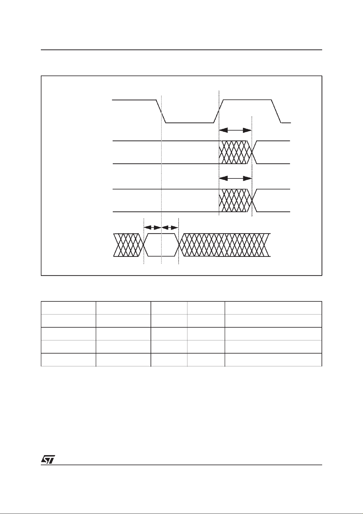
Figure 10. AFE Control Interface Timing (TTL)
SPI_CL K
SPI_ENB
SPI_DT X
STLC1510
ta c c
tacc
tse
SPI_D RX
tho
Table 10. AFE Control Interface Timing
Pin Name Parameter Min. Max. Reference Pin
SPI_ENB tacc 0 5ns w.r.t. rising SPI_CLK
SPI_DTX tacc 0 5ns w.r.t. rising SPI_CLK
SPI_DRX tse 5ns w.r.t. falling SPI_CLK
SPI_DRX tho 5ns w.r.tfalling SPI_CLK
25/40

STLC1510
Figure 11. Line Driver Control Interface Timing (TTL)
CK35M
tacc
LinDr_CTRL1
LinDr_CTRL2
LinDr_AGC
Table 11. Line Driver Control Interface Timing
Pin Name Parameter Min. Max. Reference Pin
LinDr_CTRL1 tacc 0 7ns w.r.t. rising CK35M
LinDr_CTRL2 tacc 0 7ns w.r.t. rising CK35M
LinDr_AGC tacc 0 7ns w.r.t. rising CK35M
26/40

Figure 12. Test Interface Timing (TTL)
TCK
TDO
STLC1510
tacc
tse
TDI
tse
TRSTN
tho
tho
Table 12. Test Interface Timing
Pin Name Parameter Min. Max. Reference Pin
TDO tacc 0 10ns w.r.t. rising TCK
TDI tse 5ns w.r.t. rising TCK
TDI tho 5ns w.r.trising TCK
TRSTN tse 5ns w.r.t. rising TCK
TRSTN tho 5ns w.r.trising TCK
27/40

STLC1510
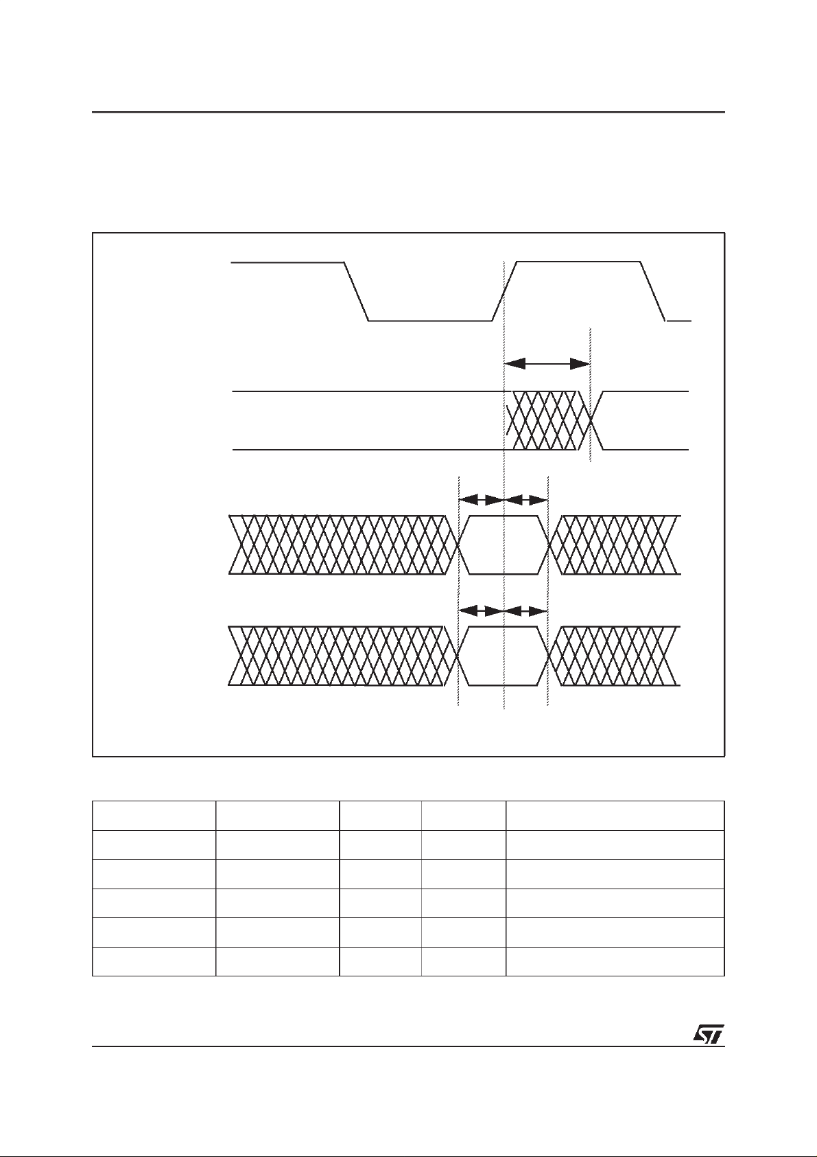
Network Interface Timing
Figure 13. UTOPIA Transmit Interface Timing
TxCLK
TxClav
tacc
tse
TxEnb
TxSOC
UTxData[7:0]
Tx Ad dr[4:0 ]
TxParity
tho
Table 13. Transmit Utopia Interface Timing
Pin Name Parameter Min. Max. Reference Pin
TxClav tacc 0 10ns w.r.t. rising TxClk
TxSOC tse 5ns w.r.t.rising TxClk
TxSOC tho 2ns w.r.trising TxClk
TxEnb tse 5ns w.r.t. rising TxClk
TxEnb tho 2ns w.r.trising TxClk
UTxData[7:0] tse 5ns w.r.t. rising TxClk
UTxData[7:0] tho 2ns w.r.t.rising TxClk
TxAddr[4:0] tse 5ns w.r.t. rising TxClk
TxAddr[4:0] tho 2ns w.r.trising TxClk
TxParity tse 5ns w.r.t. rising TxClk
TxParity tho 2ns w.r.trising TxClk
28/40

Figure 14. UTOPIA Receive Interface Timing
RxCLK
RxClav
RxSOC
U R xData[7:0]
RxParity
RxEnb
R xA d dr [4:0]
tse
STLC1510
tacc
tho
Table 14. Receive Utopia Interface Timing
Pin Name Parameter Min. Max. Reference Pin
RxClav tacc 0 10ns w.r.t. rising RxClk
RxEnb tse 5ns w.r.t.rising RxClk
RxEnb tho 2ns w.r.trising RxClk
RxSOC tacc 0 10ns w.r.t. rising RxClk
URxData[7:0] tacc 0 10ns w.r.trising RxClk
RxAddr[4:0] tse 5ns w.r.t. rising RxClk
RxAddr[4:0] tho 2ns w.r.t.rising RxClk
RxParity tacc 5ns w.r.t. rising RxClk
29/40

STLC1510
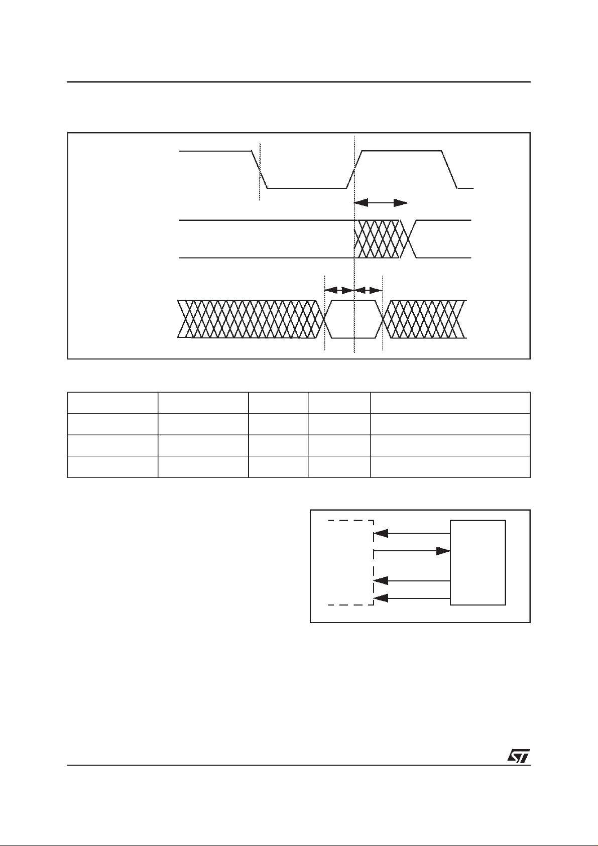
Figure 15. Serial Transmit Interface Timing
TxClk
tse
tho
UTxData[0]
Table 15. Transmit Serial Interface Timing
Pin Name Parameter Min. Max. Reference Pin
TxClk frequency
UTxData[0] tse 0ns w.r.t. rising TxClk
UTxData[0] tho 0ns w.r.t.rising TxClk
Figure 16. Serial Receive Interface Timing
RxClk
tac c
UR xData[0]
Table 16. Receive Serial Interface Timing
Pin Name Parameter Min. Max. Reference Pin
RxClk frequency
URxData[0] tacc 0 3ns w.r.t. falling RxClk
30/40

Host Processor Interface Timing
Figure 17. Host Processor Interface Timing (TTL)
HPI_BS
STLC1510
tse
tho
HPI_Addr[2:0]
HPI_RWN,HPI_CSN
HPI_D a ta[7 :0]
tacc
H PI_ D ata[7 :0]
Table 17. Host Processor Interface Timing
Pin Name Parameter Min. Max. Reference Pin
HPI_Addr[2:0] tse 2.45ns w.r.t. rising HPI_BS
HPI_Addr[2:0] tho 0.01ns w.r.t. rising HPI_BS
HPI_CSN tse 3.1ns w.r.t. rising HPI_BS
HPI_CSN tho 0.01ns w.r.t. rising HPI_BS
HPI_RWN tse 0.84ns w.r.t. rising HPI_BS
HPI_RWN tho 0.01ns w.r.t. rising HPI_BS
HPI_Data[7:0] tse 2.15ns w.r.t. rising HPI_BS
HPI_Data[7:0] tho 0.01ns w.r.t. falling HPI_CSN
HPI_Data[7:0] tacc 10ns w.r.t. falling HPI_CSN
7.2.2 GPIO Interface Timing
The GPIO[7:0] pins are memory mapped programmable pins. These pins can be programmed as input
or output providing visibility to internal chip access
points, as well as an ability to latch external control
signals. A specialmode can be configured where the
LAMBA Bus Clock is made available on a configured
output pin GPIO[0]. For timing characterization, this
mode should be used to exercise the GPIO[7:1] pins
as both inputs and outputs. The diagram below refers
to this special mode.
31/40
STLC1510
Figure 18. GPIO Interface Timing
G PIO [0]
GP IO [1:7]
tacc
tse
GPIO[1:7]
tho
Table 18. GPIO Interface Timing
Pin Name Parameter Min. Max. Reference Pin
GPIO[1:7] tacc 0 10ns w.r.t. rising GPIO[0]
GPIO[1:7] tse 5ns w.r.t. rising GPIO[0]
GPIO[1:7] tho 2ns w.r.t. rising GPIO[0]
7.3 Power-up supply sequencing
Figure 19. The NIF Serial Interface
There are two power supply voltages that must be
applied to this chip to ensure correct functionality,
(3.3V and 2.5V). The chip itself will function correctly
regardless of the sequence in which the supplies are
applied on power-up.
However if the 3.3V supply is off and there isexternal
5V activity at the IOs, the internal ESD protection circuitry will clamp the external signalsat 2.8 Volts max-
Ne twork
TxClk
UTxData[0]
RxClk
URxData[0]
imum (by sinking as much current as provided by the
interface).
In the Tx direction, the reception of a data byte from
8.0 EXTERNAL INTERFACE TIMING
the network starts with the most significant bit. Bits
are sampled by STLC1510 on the rising edge of Tx-
8.1 NIF (Network Interface) Serial Interface
The NIF serial interface consists of separate clock
and data lines inthe RXand TX directions. This interface is illustrated briefly in Figure 19.
Clk. In the presence of clock gapping (which is generated by the STLC1510, as it supplies the clocks in
both directions), a previous bit persists until the next
rising edge of the clock. Figure 21. shows the relationship between TxClk and UTxData[0].
STLC1510
32/40
Figure 20. Network Serial Interface Tx Timing
TxClk
STLC1510
UTxData[0]
B(1)
B(0) B(7) B(6) B (5) B (4)
In the Rx direction, the most significant bit of a data
byte is transmitted to the network first, with the least
significant bit transmitted last. The serial data stream
is sampled by the network on the rising edge of Rx-
Figure 21. Network Serial Interface Rx Timing
RxClk
URxData[0]
B(1)
B(0)
X
Figure 22. The NIF Utopia Level 2 Interface
TxClk
UTxData[7:0]
Tx A d d r[4 :0 ]
TxEnb
TxSO C
TxParity
TxClav
TxBP
Network
(ATM
Layer)
RxClk
URxData[7:0]
RxAddr[4:0]
RxEnb
RxSOC
RxParity
RxClav
STLC1510
(MPHY
Layer)
Clk. Samples at the gapped positions are ignored.
Figure 21. illustrates the Rx timing diagram of the serial interface. Ignored samples are indicated by ’X’ in
the timing diagram.
B(7)
B(6)
X
X
B(5)
8.2 UTOPIA Level 2 Interface
The Utopia Level 2 Interface is an 8-bit interface, operating independently in the TX and RX directions.
The Utopia Level 2 Interface is briefly illustrated in
Figure 22.
General features:
■
Implemented according to The ATM Forum
Technical Committee’s Utopia Level 2
specification. Utopia Level 2is an extension of
Utopia Level 1 which provides for connecting
multiple MPHY layer devices to a single ATM
layer. Once a given MPHY layer device has
been selected for data transfer according tothe
mechanisms specified in Utopia Level 2, the
transfer itself is performed according to the
mechanisms specified in Utopia Level 1.
■
8-bit data transfer in each direction (TX and
RX), with a maximum clock speed of
approximately 21 MHz.
■
Clocks are provided bythe ATM layer through
the TxClk and RxClk ports. (ATM layer is the
master, PHY layer is the slave)
■
There are 5address lines for each ofthe TX and
RX interfaces. Up to 31 addresses are
supported, withthe 32ndaddress (11111) being
a reserved, idle address. Single PHY operation
is supported by leaving the address lines set to
the address of the PHY device.
■
For more information, please see the ATM
33/40
STLC1510
Forum Technical Committee’s Utopia Level 1
and Utopia Level 2 specifications, and Chapter
7 of this document, Network Interface and
Controller (NIF).
Features of MPHY Layer Cell-Level Handshake (Tx
Direction):
■
A single MPHY port at a time is selected for a
cell transmission. However, another MPHY port
may be polled for its TxClav status while the
selected MPHY port transfers data. The ATM
layer polls the TxClav status of a MPHY port by
placing its address on TxAddr. The MPHY port
(STLC1510 device) drives TxClav during each
cycle following one with its address on the
TxAddr lines.
■
The ATM layer selects a MPHY port for transfer
by placing the desired MPHY address onto
TxAddr, when TxEnb is deasserted (high)
during the current clock cycle, and asserted
(low) during the next clock cycle. All MPHY
devices only examine the value on TxAddr for
selection purposes when TxEnb is deasserted
(high). The MPHY port is selected starting from
the cycle after its address ison the TxAddrlines,
and TxEnb is deasserted (high); and ending in
the cycle a new MPHY port is addressed for
selection, and TxEnb is deasserted (high).
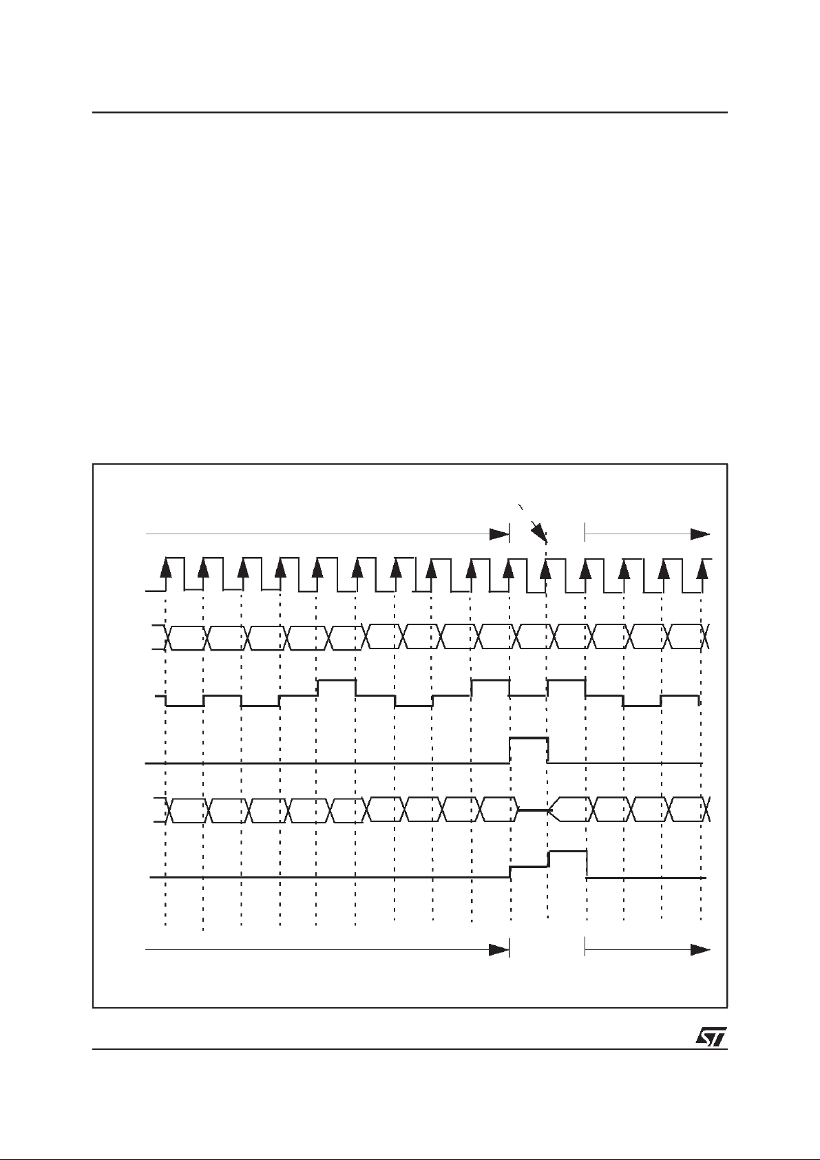
Figure 23. depicts the polling phase and the selection
phase of the UTOPIA2 transmit interface. After the
selection of the MPHY port, the cell transfer is executed the same way as in UTOPIA Level 1.
Figure 23. UTOPIA Level 2 transmit timing, polling phase and selection phase.
selection
po lling polling
TxClk
TxAddr
TxClav
TxEnb
UTxData
TxSOC
Cell transmission to:
1F 1F 1F
P40 P41 P42 P43
N+1N+3N-1
N+3
N-1
P44 P45
PHY N PHY N+3
1F 1F 1F 1F
NN+3
N+1
P46 P47
N+3N
P48 H1 H 2 H3 H 4
N+1
N+1
N-1
34/40
STLC1510
The TxBP pin is not part of the Utopia Level 2 specification, but its functionality does not interfere with
the operation of the Utopia Level 2 Interface. It canbe
left unconnected if necessary for a given application.
This signal is described in more detail in the NIF
chapter of this document.
RxAddr lines.
■ The ATM selects an MPHY port for transfer by
placing the desired MPHY port address onto
RxAddr, when RxEnb is deasserted (high)
during the current clock cycle and asserted
(low) during the following clock cycle. All MPHY
devices examine the value on RxAddr for
Features of MPHY Layer Cell-Level Handshake (Rx
Direction):
selection purposes when RxEnb is deasserted
(high). The MPHY port is selected starting from
the cycle after its address is on the RxAddr
■
A single MPHY port at a time is selected for a
cell transmission. However, another MPHY port
may be polled for its RxClav status while the
selected MPHY port transfers data. The ATM
lines, and RxEnb is deasserted (low); and
ending in the cycle a new MPHY port is
addressed for selection, and RxEnb is
deasserted (high).
layer polls the RxClav status of a MPHY port by
placing its address on RxAddr. The MPHY port
(STLC1510 device) drives RxClav during each
cycle following one with its address on the
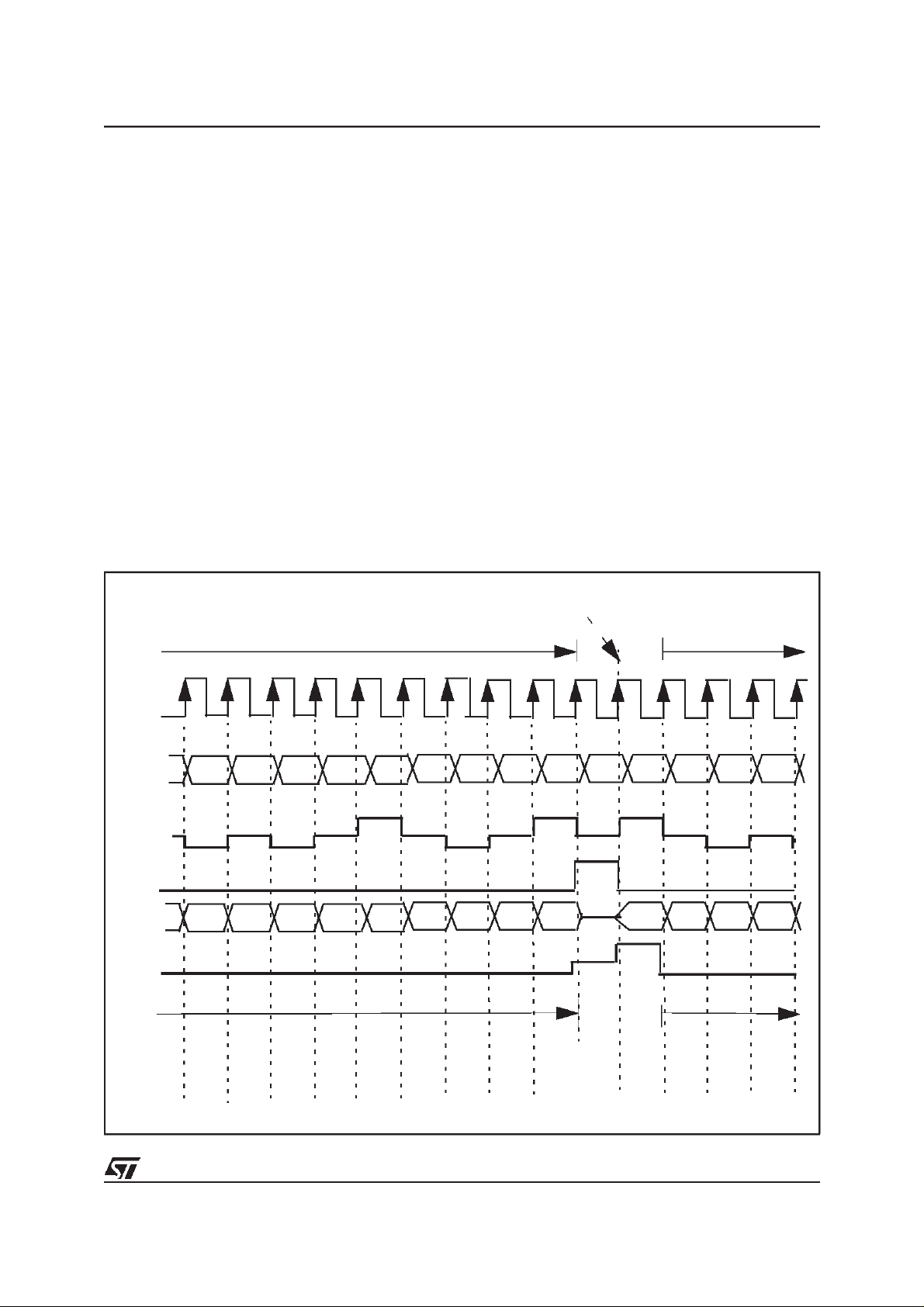
Figure 24. illustrates the timing diagram of the receive interface when a cell is received from PHY N
and theother PHYs are polled.
Figure 24. UTOPIA Level 2 receive timing, polling phase and selection phase.
sele ctio n
RxC lk
RxAddr
RxClav
RxEnb
URxData
RxSOC
C ell tra ns missio n fro m:
1F 1F 1F
P40 P41 P42 P43
po lling po l ling
N+1N+3N-1
N+3
N-1
P44 P45
PHY N PHY N+3
1F 1F 1F 1F
NN+3
N+1
P46 P4 7
P48 H1H2H3H4
N+3N
N+1
N+1
N-1
35/40

STLC1510
Figure 25. HPI Block Diagram
8.3 Host Processor Interface (HPI)
A host processor interface is provided to allow the
STLC1510 to be controlled by an external microcontroller. The design has been optimized for the Motorola MPC850. More details are provided in the EPM
STLC 1510
HPI
ARM2HP_INT
HPI_CSN
HPI_RWN
HPI_ASN
HPI_ADDR[2:0]
HPI_DATA[7:0]
HPI_CLK
External
Ho s t
Processo r
section of this document.
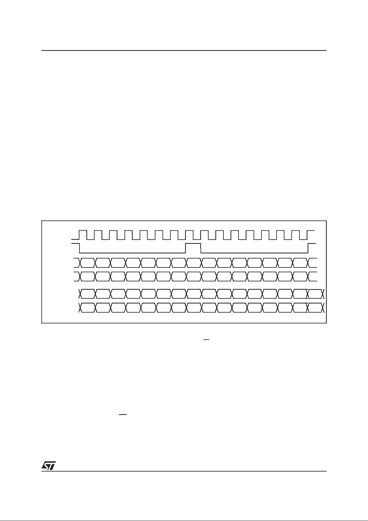
Figure 26. Host Processor Interface Timing Diagram
HPI_CLK
H P I_ Add r[2 :0 ]
HPI_CSN
HPI_ASN
HPI_RWN
H P I_ Da ta[7 :0 ]
0ns 25ns 50ns 75ns 100ns
WRITEWRITEREADREAD
addr_ su
csn_su
asn_su
rwn_ su
tda t_ su
trwn_dat_hztwrdat_valid
tdat_h
36/40
STLC1510
8.4 AFE Interface
The interface to the companion Analog Front-end device (STLC1511) operates ata rate of 35.328MHz. It
consists of two types:
■ A serial signal interface for transferring DAC
and ADC samples to and from the Aloha ASIC
ASIC.
■ A serial control interface for Aloha ASIC.
The serial signal interface to the Aloha ASIC provides
for transport of transmit and receive data between
the LAVA ASIC and Aloha ASIC. This is accomplished with a two bit wide data stream ineach direction plus the appropriate clocks. Refer to Figure 27.
for the timing diagram of this interface.
The serial signal interface consists of six pins:
■ A 35.328MHz continuous clock output
CK35M
(
);
■
A dual serial pin input pin for ADC samples
(RxSIN);
• It can carry up to 16 bits. The exact
number of bits carried is programmable
between 12 and 16. Refer to the AFE
interface definition for details.
■ A dual serial pin output pin for DAC samples
(TxSOUT);
■
It can carry up to 16 bits. The exact number of
bits carried is programmable between 14 and
16. Refer to the AFE interface definition for
details
■ An ADC and DAC sample clock input
(A_SCLK).
■
ForTX and RXinterface, data is sent on positive
edge of clock and sampled by the receiver on
the negative edge of the clock.
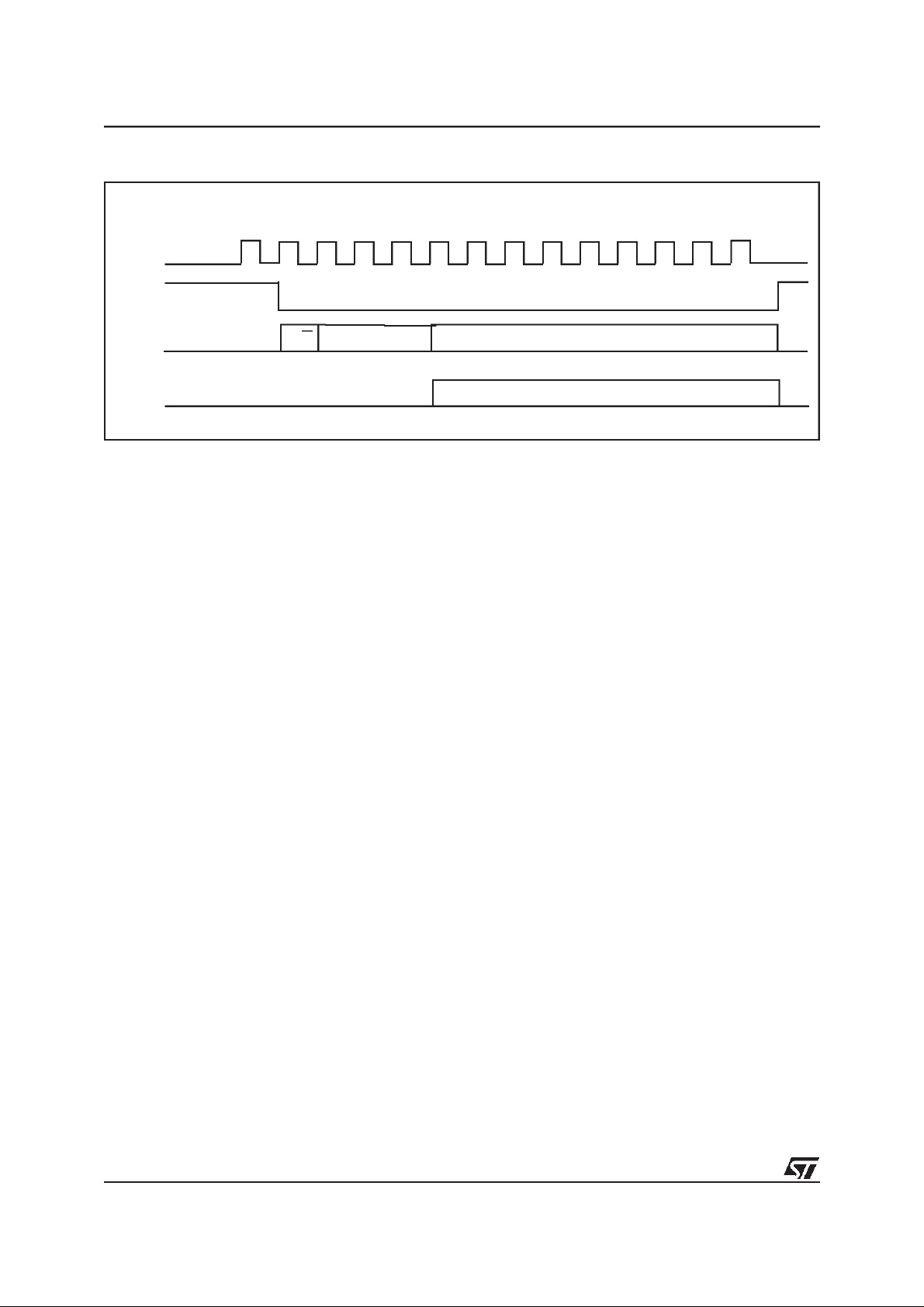
Figure 27. AFE ADC/DAC Sample Serial Interface Timing Diagram
C K35M
A _SC LK
TxSO UT[0]
TxSO UT[1]
RxSIN[0]
R xSIN [1]
a7
a15a6a1 4a5a13a4a12a3a11a2a1 0a1a9a0a8
b7
b15b6b14b5b1 3b4b12b3b11b2b10b1b9
The serial control I/F consists of 4 pins:
■
SPI_CLK: a gated 35.328MHz clock.
It is only
present during digital I/Fread/write cyclesand is
inactive otherwise.
■ SPI_ENB: an active lowenable pin which allows
selection between different AFEs if required.
■
SPI_DTX: an output data pin which is used to
send control information to the AFE ASIC.
■ SPI_DRX: an input data pin which is used
receive control information from the AFE ASIC.
It is enabled only when
R/W
is low.
b0
b8
The format for the serial interface is given below:
■
R/W
- determines the access mode for the
register
■
ADDR[b2:b0]
address[b1:b0]
.
- identifies the control register
accessed. These registers will correspond to
the mapping in the LAVA ASIC.
■
WR_DATA[b7:b0]
- the control data written to
the AFE ASIC.
37/40
STLC1510
Figure 28. AFE Control Interface Timing Diagram
SPI_CLK
(35M Hz)
SPI_ENB
SPI_DTX
SPI_DRX
R/W
AD DR ESS
[b2:b 0]
WR _D ATA{b7: b0]
R D_D ATA {b7:b0]
38/40
STLC1510
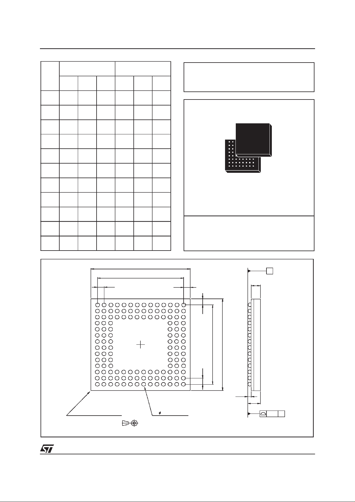
mm inch
DIM.
MIN. TYP. MAX. MIN. TYP. MAX.
A 1.210 1.700 0.047 0.067
A1 0.270 0.010
A2 1.120 0.044
b 0.450 0.500 0.550 0.018 0.02 0.021
D 11.75 12.00 12.15 0.462 0.472 0.478
D1 10.40 0.409
E 11.75 12.00 12.15 0.462 0.472 0.478
E1 10.40 0.409
e 0.720 0.800 0.880 0.028 0.031 0.034
f 0.650 0.800 0.950 0.025 0.031 0.037
ddd 0.120 0.004
OUTLINE AND
MECHANICAL DATA
Body: 12 x 12 x 1.7mm
LFBGA132
A1 CORNER INDEX
D
D1
e
P
N
M
L
K
J
H
G
F
E
D
C
B
A
1 2 3 4 5 6 7 8 9 10 11 12 13
AREA
(SEE NOTE.3)
BOTTOM VIEW
f
14
b (132 BALLS)
TING
SE
C
PLANE
A2
f
E
E1
e
A1
A
C
ddd
7146828
39/40

STLC1510
Information furnished is believed to be accurate and reliable. However, STMicroelectronics assumes no responsibility for the consequences
of use of such information nor for any infringement of patents or other rights ofthird parties which may result from its use. No license is granted
by implicationor otherwise under any patent or patent rights of STMicroelectronics. Specifications mentioned in this publication are subject
to change without notice. This publication supersedes and replaces all information previously supplied. STMicroelectronics products are not
authorized for use as critical components in life support devices or systems without express written approval of STMicroelectronics.
The ST logo is a registered trademark of STMicroelectronics
2000 STMicroelectronics - All Rights Reserved
Australia - Brazil - China - Finland - France - Germany - Hong Kong - India - Italy - Japan - Malaysia - Malta - Morocco - Singapore - Spain
STMicroelectronics GROUP OF COMPANIES
- Sweden - Switzerland - United Kingdom - U.S.A.
http://www.st.com
40/40
 Loading...