


查询STGB7NC60HD供应商
N-CHANNEL 14A - 600V - TO-220/TO-220FP/D²PAK
STGP7NC60HD
STGF7NC60HD - STGB7NC60HD
Very Fast PowerMESH™ IGBT
Table 1: Ge neral Features
TYPE V
STGP7NC60HD
STGF7NC60HD
STGB7NC60HD
■ LOWER ON-VOLTAGE DROP (V
■ OFF LOSSES INCLUDE TAIL CURRENT
■ LOSSES INCLUDE DIODE RECOVERY
CESVCE(sat)
600 V
600 V
600 V
(Max)
@25°C
< 2.5 V
< 2.5 V
< 2.5 V
cesat
I
C
@100°C
14 A
6 A
14 A
)
ENERGY
■ LOWER C
■ HIGH FREQUENCY OPERATION UP TO 70
RES/CIES
RATIO
KHz
■ VERY SOFT ULTRA FAST RECOVERY ANTI
PARALLEL DIODE
■ NEW GENERATION PRODUCTS WITH
TIGHTER PARAMETER DISTRIBUTION
DESCRIPTION
Using the latest high voltage technology based on
a patented strip layout, STMicroelectronics has
designed an advanced family of IGBTs, the PowerMESH
™
IGBTs, with outstanding performances.
The suffix "H" identifies a family optimized for high
frequency applications in order to achieve very
high switching performances (reduced tfall) mantaining a low voltage drop.
Figure 1: Package
3
2
1
TO-220
3
1
TO-220FP
D2PAK
Figure 2: Internal Schematic Diagram
3
2
1
APPLICATIONS
■ HIGH FREQUENCY INVERTERS
■ SMPS AND PFC IN BOTH HARD SWITCH
AND RESONANT TOPOLOGIES
■ MOTOR DRIVERS
Table 2: Order Code
PART NUMBER MARKING PACKAGE PACKAGING
STGP7NC60HD GP7NC60HD TO-220 TUBE
STGF7NC60HD GF7NC60HD TO-220FP TUBE
STGB7NC60HDT4
GB7NC60HD
2
D
PAK
TAPE & REEL
Rev.9
1/15June 2005
STGP7NC60HD - STGF7N C60HD - STGB7NC60HD
Table 3: Absolute Maxim u m ra t in gs
Symbol Parameter Value Unit
STGP7NC60HD
STGB7NC60HD
Collector-Emitter Voltage (VGS = 0)
Emitter-Collector Voltage 20 V
Gate-Emitter Voltage ±20 V
GE
Collector Current (continuous) at TC = 25°C (#)
C
Collector Current (continuous) at TC = 100°C (#)
C
()
Collector Current (pulsed) 50 A
I
Diode RMS Forward Current at TC = 25°C
F
Total Dissipation at TC = 25°C
25 10 A
14 6 A
80 25 W
I
V
V
V
CM
P
CES
ECR
I
I
TOT
Derating Factor 0.64 0.20 W/°C
V
T
Insulation Withstand Voltage A.C.(t = 1 sec; Tc = 25°C) -- 2500 V
ISO
Storage Temperature
stg
T
Operating Junction Temperature
j
– 55 to 150 °C
() Pulse wid th limited by max . ju nct i on temperature.
Table 4: Thermal Data
Rthj-case Thermal Resistance Junction-case TO-220
D²PAK
TO-220FP 5.0 °C/W
Rthj-amb Thermal Resistance Junction-ambient 62.5 °C/W
T
L
Maximum Lead T emperature for Soldering Purpose
(1.6 mm from case, for 10 sec.)
STGF7NC60HD
600 V
20 A
Min. Typ. Max.
1.56 °C/W
300 °C
ELECTRICAL CHARACTERISTICS (T
=25°C UNLESS OTH ERWI SE SPEC IFIED)
CASE
Table 5: Main Parameters
Symbol Parameter Test Conditions Min. Typ. Max. Unit
V
BR(CES)
Collector-Emitter Breakdown
Voltage
I
CES
I
GES
V
GE(th)
V
CE(sat)
Collector cut-off Current
= 0)
(V
GE
Gate-Emitter Leakage
Current (V
CE
= 0)
Gate Threshold Voltage
Collector-Emitter Saturation
Voltage
(#) Calculated according to the iterative formu l a:
T
–
ICTC()
--------------------------------------------------------------------------------------------------
=
R
THJ C–
JMAXTC
V
CESAT MAX()TCIC
2/15
,()×
IC = 1 mA, VGE = 0 600 V
V
= Max Rating, TC = 25 °C
CE
VCE = Max Rating, TC = 125 °C
V
= ± 20V , VCE = 0 ±100 nA
GE
V
= VGE, IC = 250 µA
CE
VGE = 15V, IC = 7 A
V
= 15V, IC = 7 A, Tc= 125°C
GE
3.75 5.75 V
1.85
1.7
10
1
mA
2.5 V
µA
V
STGP7NC60HD - STGF7N C60HD - STGB7NC60HD
ELECTRICAL CHARACTERISTICS (CONTINUED)
Table 6: Dynamic
Symbol Parameter Test Conditions Min. Typ. Max. Unit
(1)
g
fs
C
ies
C
oes
C
res
Forward Transconductance
Input Capacitance
Output Capacitance 81 pF
Reverse Transfer
Capacitance
Q
g
Q
ge
Q
gc
I
CL
Total Gate Charge
Gate-Emitter Charge
Gate-Collector Charge
Turn-Off SOA Minimum
Current
(1) Pulsed: Pulse durati on= 300 µs, dut y c yc l e 1.5%
Table 7: Switching On
Symbol Parameter Test Conditions Min. Typ. Max. Unit
t
d(on)
t
(di/dt)
t
d(on)
t
(di/dt)
r
r
Turn-on Delay Time
Current Rise Time
Turn-on Current Slope
on
Turn-on Delay Time
Current Rise Time
Turn-on Current Slope
on
VCE = 15 V , IC= 7 A 4.30 S
V
= 25 V, f= 1 MHz, VGE = 0
CE
720 pF
17 pF
= 390 V, IC = 7 A,
V
CE
VGE = 15 V
(see Figure 22)
V
= 480 V , Tj = 150°C
clamp
R
= 10 Ω, VGE = 15 V
G
VCC = 390 V, IC = 7 A
R
=10 Ω, VGE= 15V, Tj= 25°C
G
(see Figure 19)
VCC = 390 V, IC = 7 A
RG=10 Ω, VGE= 15V , Tj= 125°C
(see Figure 20)
50 A
35
7
16
18.5
8.5
1060
18.5
7
1000
48 nC
nC
nC
ns
ns
A/µs
ns
ns
A/µs
Table 8: Switching Off
Symbol Parameter Test Conditions Min. Typ. Max. Unit
t
r(Voff
t
d(off
t
r(Voff
t
d(off
)
Off Voltage Rise Time
)
Turn-off Delay Time 72 ns
t
f
t
f
Current Fall Time 60 ns
)
Off Voltage Rise Time
)
Turn-off Delay Time 116 ns
Current Fall Time 105 ns
Vcc = 390 V, IC = 7 A,
R
= 10 Ω , VGE = 15 V
G
TJ = 25 °C
(see Figure 20)
Vcc = 390 V, IC = 7 A,
R
= 10 Ω , VGE = 15 V
G
Tj = 125 °C
(see Figure 20)
27 ns
56 ns
Table 9: Switching Energy
Symbol Parameter Test Conditions Min. Typ. Max Unit
Eon (2)
E
off
E
ts
Eon (2)
E
off
E
ts
(2) Eon i s t he tur n-on l oss es wh en a typ ica l diod e is used in th e tes t cir cui t in fig ure 2. I f the IGB T is o ffere d in a pac kage w it h a co- pa ck
diode, the co-pack diode is used as external diode. IGBTs & DIODE are at the same temperature (25°C and 125°C)
(3) Turn-off losses in clude also the tail of the collector current.
Turn-on Switching Losses
Turn-off Switching Loss
(3)
Total Switching Loss
Turn-on Switching Losses
Turn-off Switching Loss
(3)
Total Switching Loss
= 390 V, IC = 7 A
V
CC
R
= 10 Ω, VGE= 15V, Tj= 25°C
G
(see Figure 19)
= 390 V, IC = 7 A
V
CC
RG= 10 Ω, VGE= 15V, Tj= 125°C
(see Figure 20)
95
115
210
140
215
355
125
150
275
µJ
µJ
µJ
µJ
µJ
µJ
3/15
STGP7NC60HD - STGF7N C60HD - STGB7NC60HD
Table 10: Collector-Emitter Diode
Symbol Parameter Test Condiction Min. Typ. Max. Unit
Q
I
Q
I
V
t
rr
t
a
rrm
S
t
rr
t
a
rrm
S
Forward On-Voltage If = 3.5 A
f
If = 3.5 A, Tj = 125 °C
Reverse Recovery Time
rr
Reverse Recovery Charge
If = 7 A, V
= 25 °C, di/dt = 100 A/µs
T
j
= 40 V,
R
Reverse Recovery Current
Softness factor of the diode
Reverse Recovery Time
rr
Reverse Recovery Charge
If = 7 A, V
= 125 °C, di/dt = 100 A/µs
T
j
= 40 V,
R
Reverse Recovery Current
Softness factor of the diode
1.3
1.1
37
22
40
2.1
0.68
61
34
98
3.2
0.79
1.9
V
V
ns
ns
nC
A
ns
ns
nC
A
4/15
STGP7NC60HD - STGF7N C60HD - STGB7NC60HD
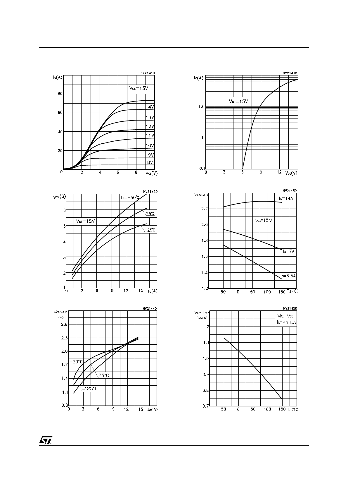
Figure 3: Output Characteristics
Figure 4: Transconductance
Figure 6: Transfer Characteristics
Figure 7: Collector-Emitter On Voltage vs Temperature
Figure 5: Collector-Emitter On Voltage vs Collector Curr e nt
Figure 8: Normalized Gate Threshold vs Temperature
5/15
 Loading...