

查询STGP7NB120SD供应商
STGP7NB120SD
N-CHANNEL 7A - 1200V -TO-220
PowerMESH™ IGBT
TYPE V
CES
V
CE(sat)
I
C
STGP7NB120SD 1200 V < 2.1 V7A
■ HIGH INPUT IMPEDANCE (VOLTAGE DRIVEN)
■ VERY LOW ON-VOLTAGE DROP (V
■ OFF LOSSES INCLUDE TAIL CURRENT
■ HIGH CURRENT CAPABILITY
cesat
)
DESCRIPTION
Using the lates t high voltage technology based on a
patented strip layout, STMicroelectronics has
designed an advanced family of IGBTs, the
PowerMESH
™
IGBTs, with outstanding
performances. The suffix “S” identifies a f amily
optimized achieve minimum on-v oltage drop for low
frequency applications (<1kHz).
APPLICATIONS
■ MOTOR CONTROL
■ LIGHT DIMMER
■ INTRUSH CURRENT LIMITATION
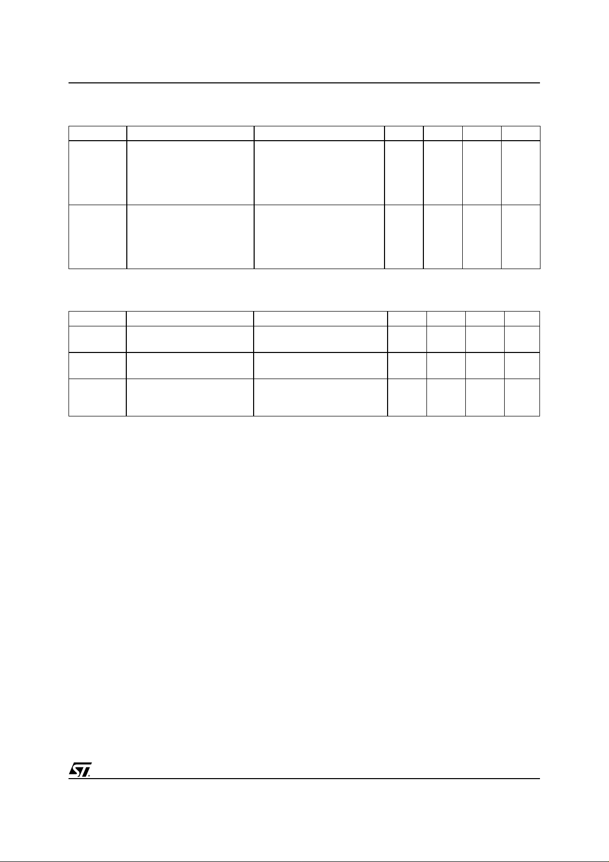
3
2
1
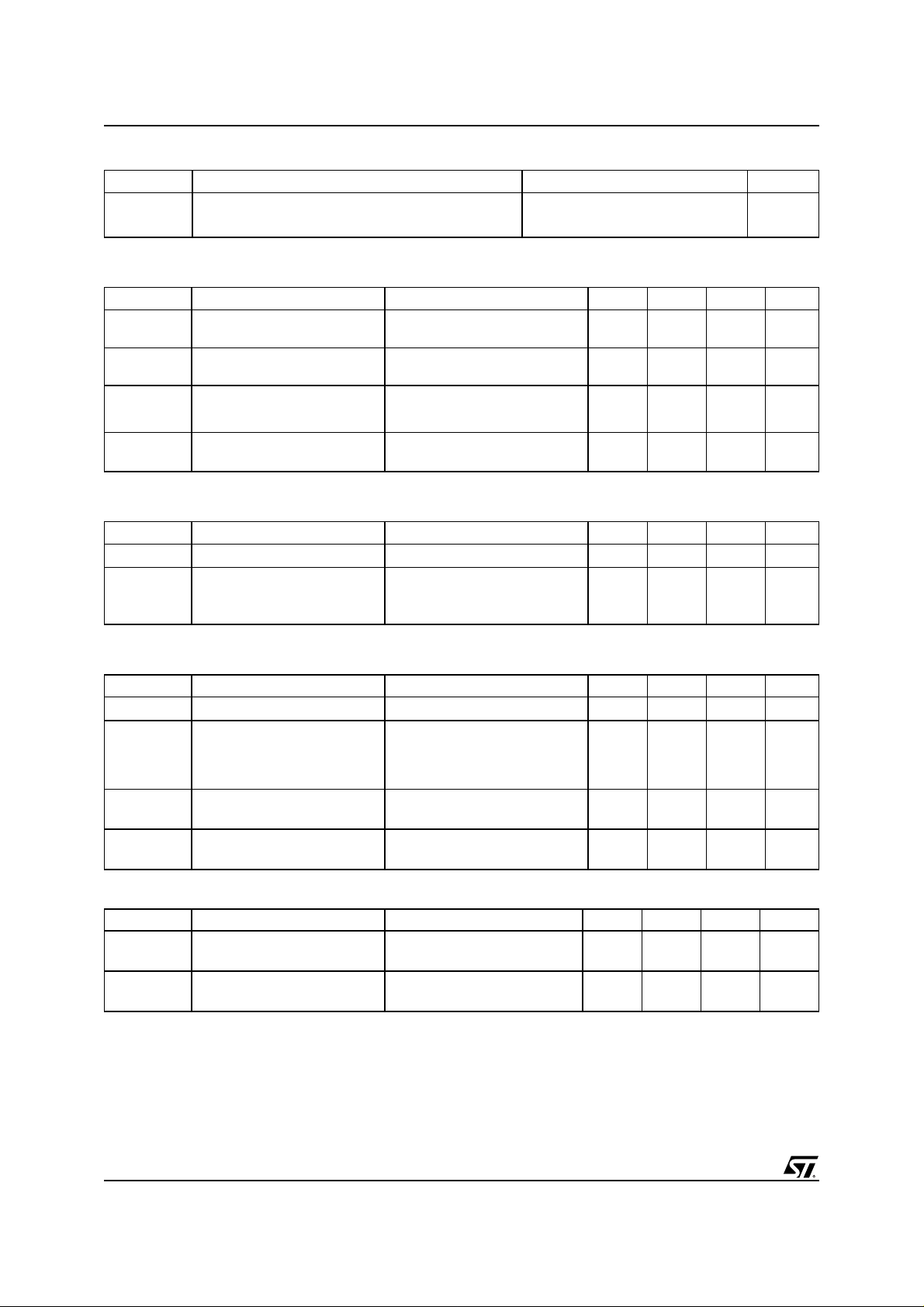
TO-220
INTERNAL SCHEMATIC DIAGRAM
ABSOLUTE MAXIMUM RATINGS
Symbol Parameter Value Unit
V
CES
V
ECR
V
GE
I
C
I
C
I
CM
P
TOT
T
stg
T
j
Collector-Emitter Voltage (VGS=0)
1200 V
Reverse Battery Protection 20 V
Gate-Emitter Voltage ±20 V
Collector Current (continuous) at TC=25°C
Collector Current (continuous) at TC=100°C
()
Collector Current (pulsed) 20 A
Total Dissipation at TC= 25°C
10 A
7A
90 W
Derating Factor 0.7 W/°C
Storage Temperature –65 to 150 °C
Max. Operating Junction Temperature 150 °C
(●) Pulsewidthlimited by safeoperatingarea
1/8November 2002
STGP7NB120SD
THERMAL DATA
Rthj-case Thermal Resistance Junction-case Max 1.38 °C/W
Rthj-amb Thermal Resistance Junction-ambient Max 62.5 °C/W
Rthc-h Thermal Resistance Case-heatsink Typ 0.5 °C/W
ELECTRICAL CHARACTERISTICS (T
= 25 °C UNLESS O THERWISE SPECIFIED)
CASE
OFF
Symbol Parameter Test Conditions Min. Typ. Max. Unit
V
BR(CES)
Collector-Emitter Breakdown
IC= 250 µA, VGE= 0 1200 V
Voltage
V
BR(ECR)
Emitter-Collector Breakdown
IC= 10mA, VGE= 0 20 V
Voltage
I
CES
I
GES
Collector cut-off
=0)
(V
GE
Gate-Emitter Leakage
Current (V
CE
=0)
V
= Max Rating, TC=25°C
CE
VCE= Max Rating, TC= 125 °C
V
=±20V,VCE= 0 ±100 nA
GE
50 µA
250 µA
ON (1)
Symbol Parameter Test Conditions Min. Typ. Max. Unit
V
GE(th)
V
CE(sat)
Gate Threshold Voltage
Collector-Emitter Saturation
Voltage
V
CE=VGE,IC
VGE=15V,IC= 3.5 A
VGE=15V,IC=7A
=15V,IC=10A
V
GE
= 250µA
35V
1.6
2.1
1.7
DYNAMIC
Symbol Parameter Test Conditions Min. Typ. Max. Unit
V
g
fs
C
ies
C
oes
C
res
Q
g
I
CL
Forward Transconductance
Input Capacitance
Output Capacitance
Reverse Transfer
Capacitance
Gate Charge VCE= 960V, IC=7A,
Latching Current V
=25V,IC=7 A
CE
=25V,f=1MHz,VGE= 0 430
V
CE
V
=15V
GE
= 960V , Tj = 150°C
clamp
2.5 4.5 S
10 A
RG=1KΩ
40
7
29 nC
V
V
V
pF
pF
pF
SWITCHING ON
Symbol Parameter Test Conditions Min. Typ. Max. Unit
=960V,IC=7A
V
CC
=1KΩ,VGE=15V
R
G
= 960 V,IC= 7 A, RG=1KΩ
V
CC
VGE= 15 V,Tj = 125°C
570
270
800
3.2
2/8
t
d(on)
t
(di/dt)
Eon
Turn-on Delay Time
r
Rise Time
Turn-on Current Slope
on
Turn-on Switching Losses
ns
ns
A/µs
mJ
STGP7NB120SD
ELECTRICAL CHARACTERISTICS (CONTINUED)
SWITCHING OFF
Symbol Parameter Test Conditions Min. Typ. Max. Unit
= 960 V,IC=7A,
V
cc
=1KΩ,VGE=15V
R
GE
V
= 960 V,IC=7A,
cc
R
=1KΩ,VGE=15V
GE
Tj = 125 °C
If= 3.5 A, Tj = 125 °C
= 3.5 A ,VR= 600 V,
I
f
Tj =125°C, di/dt = 100A/µs
4.9
7.5
1.7
1.5
190
850
3.5
28
2.0
9
t
r(Voff
E
tr(V
E
t
c
t
f
(**)
off
t
c
off
t
f
(**)
off
Cross-over Time
)
Off Voltage Rise Time 2.9
Fall Time 3.3
Turn-off Switching Loss 15
Cross-over Time
)
Off Voltage Rise Time 5.5
Fall Time 6.2
Turn-off Switching Loss 22
COLLECTOR-EMITTER DIODE
Symbol Parameter Test Conditions Min. Typ. Max. Unit
I
f
I
fm
V
f
t
rr
Q
rr
I
rrm
Note: 1. Pulsed: Pulse duration = 300 µs, duty cycle 1.5 %.
2. Pulse width limited by max. junction temperature.
(**)Losses include Also the Tail (Jedec Standardization)
Forward Current
Forward Current pulsed
Forward On-Voltage If=3.5 A
Reverse Recovery Time
Reverse Recovery Charge
Reverse Recovery Current
µs
µs
µs
mJ
µs
µs
µs
mJ
A
A
V
V
ns
nC
A
3/8

STGP7NB120SD
Turn-Off Energy Losses vs Tem peratureThermal Impedance
Output Characteristics
Transfer Characteristics
TransconductanceNormalized Gate Threshold Voltage vs Temp.
4/8

STGP7NB120SD
Gate-Charge vs Gate-Emitter VoltageCollector-Emitter On Voltage vs Temperature
Diode Forward VoltageCapacitance Variations
Collector-Emitter On Voltage vs Collector Current
5/8

STGP7NB120SD
Fig. 2: Test Circuit For Inductive Load SwitchingFig. 1: Gate Charge test Circuit
6/8

E
TO-220 MECHANICAL DATA
P011C
STGP7NB120SD
DIM.
A 4.40 4.60 0.173 0.181
C 1.23 1.32 0.048 0.051
D 2.40 2.72 0.094 0.107
D1 1.27 0.050
E 0.49 0.70 0.019 0.027
F 0.61 0.88 0.024 0.034
F1 1.14 1.70 0.044 0.067
F2 1.14 1.70 0.044 0.067
G 4.95 5.15 0.194 0.203
G1 2.4 2.7 0.094 0.106
H2 10.0 10.40 0.393 0.409
L2 16.4 0.645
L4 13.0 14.0 0.511 0.551
L5 2.65 2.95 0.104 0.116
L6 15.25 15.75 0.600 0.620
L7 6.2 6.6 0.244 0.260
L9 3.5 3.93 0.137 0.154
DIA. 3.75 3.85 0.147 0.151
MIN. TYP. MAX. MIN. TYP. MAX.
mm inch
A
C
D
L5
Dia.
L7
D1
L6
L2
L9
F1
G1
F
H2
G
F2
L4
7/8

STGP7NB120SD
Information furnished is believed to be accurate and reliable. However, STMicroelectronics assumes no responsibi lity f or the
consequences of use of su ch in formation nor for any in fringement of patents or other rights of third parties w hich may result from
its use. No license is granted by implication or otherwise under any patent or patent rights of STMicroelectronics. Specifications
mentioned in this publication are subject to change without notice. This publication supersedes and replaces all information
previously suppli ed. STMi croelect ronics pr oducts are not author ized for use as cr itical component s in li fe suppo rt devi ces or
systems without express written approval of STMicroelectronics.
Australia - Brazil - Canada - China - Finland - France - Germany - Hong Kong - India - Israel - Italy - Japan - Malaysia - Malta - Morocco
© The ST logo is a registered trademark of STMicroelectronics
© 2002 STMicroelectronics - Printed in Italy - All Rights Reserved
Singapore - Spain - Sweden - Switzerland - United Kingdom - United States.
STMicroelectronics GROUP OF COMPANIES
© http://www.st.com
8/8
 Loading...