

ST STGP12NB60K User Manual
STGP12NB60K
N-CHANNEL 18A - 600V TO-220
SHORT CIRCUIT PROOF PowerMESH™ IGBT
TYPE V
CES
V
CE(sat)
(Max) @25°C
IC(#)
@100°C
STGP12NB60K 600 V < 2.8 V18A
■ HIGH INPUT IMPEDANCE
■ LOW ON-LOSSES
■ LOW GATE CHARGE
■ HIGH CURRENT CAPABILITY
■ OFF LOSSES INCLUDE TAILCURRENT
■ VERY HIGH FREQUENCY OPERATION
■ TYPICAL SHORT CIRCUIT WITHSTAND TIME 10
MICROS
DESCRIPTION
Using the latest high voltage technology based on a
patented strip layout, STM icr oelectronics has designed an advanced family of IGBTs, the P ower-
™
MESH
IGBTs, with outstanding performances. T he
suffix “K” identifies a family optimized for hig h frequency applications (up to 50kHz ) and short circuit proof in
order to achieve very high switching performances (reduced tfall) mantaining a low voltage drop.
APPLICATIONS
■ HIGH FREQUENCY MOTOR CO NTROLS
■ SMPS
■ UPS
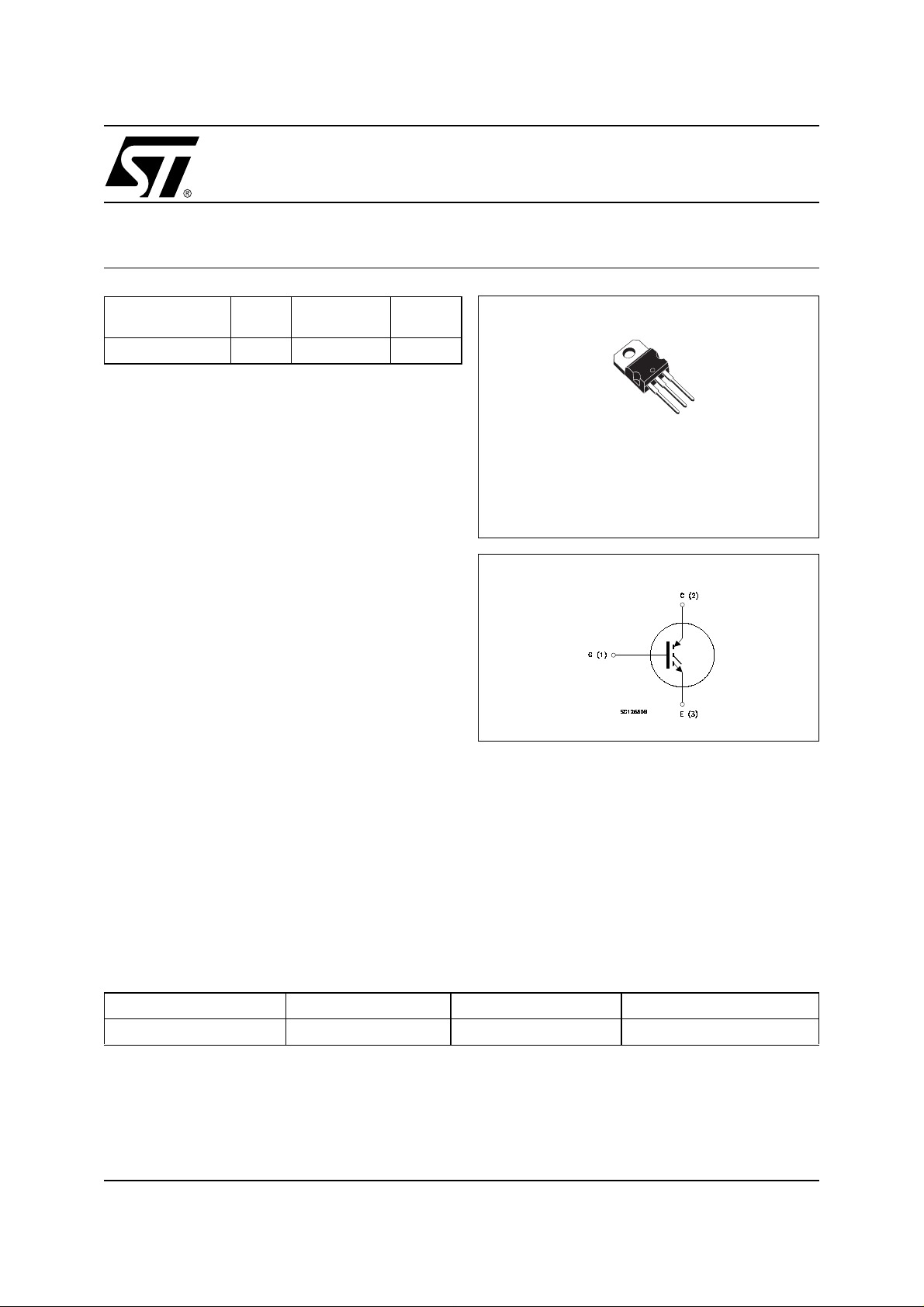
3
2
1
TO-220
INTERNAL SCHEMATIC DIAGRAM
ORDERING INFORMATION
SALES TYPE MARKING PACKAGE PACKAGING
STGP12NB60K GP12NB60K TO-220 TUBE
1/9December 2003
STGP12NB60K
ABSOLUTE MAXIMUM RATINGS
Symbol Parameter Value Unit
V
CES
V
ECR
V
GE
I
C
I
C
I
CM
Tsc Short Circuit Withstand 10
P
TOT
T
stg
T
j
() Pulsewidthlimitedbysafeoperatingarea
THERMAL DATA
Rthj-case Thermal Resistance Junction-case Max 1.0 °C/W
Rthj-amb Thermal Resistance Junction-ambient Max 62.5 °C/W
Collector-Emitter Voltage (VGS=0)
600 V
Emitter-Collector Voltage 20 V
Gate-Emitter Voltage ± 20 V
Collector Current (continuous) at TC= 25°C (#)
Collector Current (continuous) at TC= 100°C (#)
()
Collector Current (pulsed) 60 A
Total Dissipation at TC= 25°C
30 A
18 A
125 W
Derating Factor 1.0 W/°C
Storage Temperature –65 to 150 °C
Max. Operating Junction Temperature 150 °C
µs
ELECTRICAL CHARACTERISTICS (T
= 25 °C UNLESS OTHERWISE SPECIFIED)
CASE
OFF
Symbol Parameter Test Conditions Min. Typ. Max. Unit
V
BR(CES)
Collector-Emitter Breakdown
IC=250µA,VGE= 0 600 V
Voltage
I
CES
I
GES
Collector cut-off
=0)
(V
GE
Gate-Emitter Leakage
Current (V
CE
=0)
V
= Max Rating, TC=25°C
CE
V
= Max Rating, TC= 125 °C
CE
V
= ± 20V , VCE= 0 ±100 nA
GE
50
100
ON (1)
Symbol Parameter Test Conditions Min. Typ. Max. Unit
V
GE(th)
V
CE(sat)
Gate Threshold Voltage
Collector-Emitter Saturation
Voltage
V
CE=VGE,IC
VGE= 15V, IC=12A
VGE=15V,IC=12A,Tj=125°C
=250µA
57V
2.2
2.8 V
1.7
DYNAMIC
Symbol Parameter Test Conditions Min. Typ. Max. Unit
V
g
C
C
C
Q
Q
Q
I
T
Forward Transconductance
fs
Input Capacitance
ies
Output Capacitance
oes
Reverse Transfer Capacitance
res
Total Gate Charge
g
Gate-Emitter Charge
ge
Gate-Collector Charge
gc
Latching Current V
CL
Short Circuit WITHSTAND
wsc
Time
=25V,IC=12A
CE
=25V,f=1MHz,VGE=0
V
CE
VCE=480V,IC=12A,
= 15V
V
GE
= 480 V , VGE=15V,
clamp
Tj = 125°C , RG=10Ω
VCE=0.5BV
ces ,VGE
Tj = 125°C , RG=10Ω
=15V
5S
890
110
22
54
8
31
48 A
10 µs
µA
µA
V
pF
pF
pF
nC
nC
nC
2/9

STGP12NB60K
ELECTRICAL CHARACTERISTICS (CONTINUED)
SWITCHING ON
Symbol Parameter Test Conditions Min. Typ. Max. Unit
V
t
d(on)
(di/dt)
Eon
Turn-on Delay Time
t
Rise Time 14.5 ns
r
Turn-on Current Slope
on
Turn-on Switching Losses
SWITCHING OFF
Symbol Parameter Test Conditions Min. Typ. Max. Unit
t
c
tr(V
off
t
d(off
t
f
E
(**)
off
E
ts
t
c
tr(V
off
t
d(off
t
f
E
(**)
off
E
ts
Note: 1. Pulsed: Pulse duration = 300 µs, duty cycle 1.5 %.
2. Pulse width limited by max. junction temperature.
(**)Losses include Also the Tail (Jedec Standardization)
Cross-over Time
)
Off Voltage Rise Time 25 ns
)
Delay Time 96 ns
Fall Time 100 ns
Turn-off Switching Loss 258 µJ
Total Switching Loss 410 µJ
Cross-over Time
)
Off Voltage Rise Time 80 ns
)
Delay Time 150 ns
Fall Time 220 ns
Turn-off Switching Loss 650 µJ
Total Switching Loss 830 µJ
= 480 V, IC=12A
CC
=10Ω,VGE=15V
R
G
V
= 480 V, IC=12ARG=10Ω
CC
= 15 V,Tj = 125°C
V
GE
V
= 480 V, IC=12A,
cc
RGE=10Ω,VGE=15V
V
= 480 V, IC=12A,
cc
RGE=10Ω,VGE=15V
Tj = 125 °C
25 ns
590 A/µs
180 µJ
130 ns
310 ns
(#) Calculated according to the iterative formula:
–
T
ICTC()
--------------------------------------------------------------------------------------
=
R
THJ C–VCESAT MAX()
JMAXTC
T
I
,()×
C
C
3/9
 Loading...