

ST STGP12NB60HD User Manual
查询STGP12NB60HD供应商
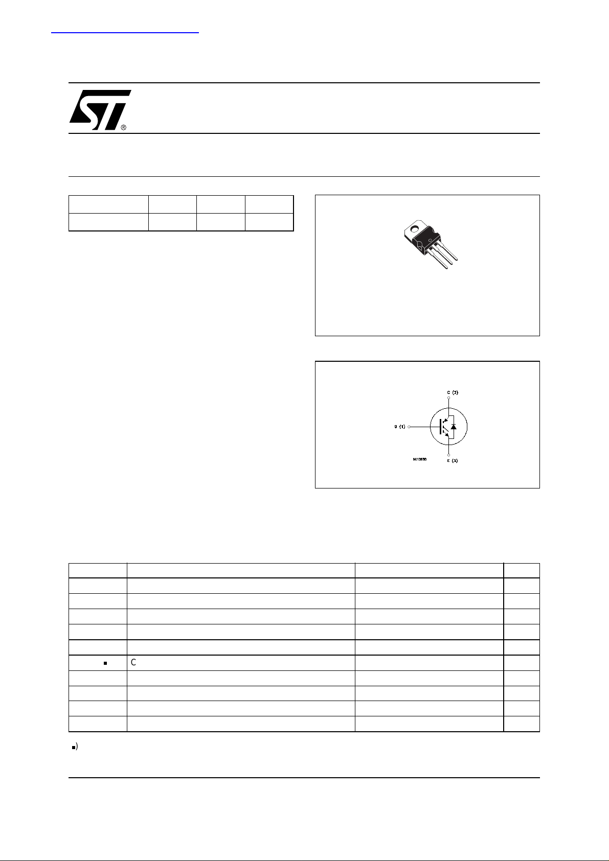
STGP12NB60HD
N-CHANNEL 12A - 600V TO-220
PowerMESH™ IGBT
TYPE V
STGP12NB60HD 600 V < 2.8 V12A
■ HIGH INPUT IMPEDANCE
■ LOW ON-VOLTAGE DROP (V
■ OFF LOSSES INCLUDE TAIL CURRENT
■ LOW GATE CHARGE
■ HIGH CURRENT CAPABILITY
■ VERY HIGH FREQUENCY OPERATION
■ CO-PACKAGED WITH TURBOSWITCHT
■ ANTIPARALLEL DIODE
CES
V
CE(sat)
cesat
I
C
)
DESCRIPTION
Using the latest high voltage technology based on a
patented strip layout, STMicroelectronics ha s designed an advanced family of IGBTs, the PowerMESH™ I GBTs, with outstanding perfomances.
The suffix "H" identifies a family o ptimized for high
frequency app lications (up to 50kHz)in o rder to
achieve very high switching performances (reduced
tfall) mantaining a low voltage drop.
APPLICATIONS
■ HIGH FREQUENCY MOTOR CONTROLS
■ SMPS and PFC IN BOTH HARD SWITCH AND
RESONANT TOPOLOGIES
■ UP S
3
2
1
TO-220
INTERNAL SCHEMATIC DIAGRAM
ABSOLUTE MAXIMUM RATINGS
Symbol Parameter Value Unit
V
CES
V
ECR
V
GE
I
C
I
C
ICM()
P
TOT
T
stg
T
j
() Pulsewidthlimitedbysafeoperatingarea
Collector-Emitter Voltage (VGS=0)
Emitter-Collector Voltage 20 V
Gate-Emitter Voltage ± 20 V
Collector Current (continuous) at TC=25°C
Collector Current (continuous) at TC=100°C
Collector Current (pulsed) 96 A
Total Dissipation at TC= 25°C
Derating Factor 0.8 W/°C
Storage Temperature –65 to 150 °C
Max. Operating Junction Temperature 150 °C
600 V
24 A
12 A
100 W
1/9July 2003
STGP12NB60HD
THERMAL DATA
Rthj-case Thermal Resistance Junction-case Max 1.25 °C/W
Rthj-amb Thermal Resistance Junction-ambient Max 62.5 °C/W
Rthc-sink Thermal Resistance Case-sink Typ 0.5 °C/W
ELECTRICAL CHARACTERISTICS (T
= 25 °C UNLESS OTHERWISE SPECIFIED)
CASE
OFF
Symbol Parameter Test Conditions Min. Typ. Max. Unit
V
BR(CES)
Collector-Emitter Breakdown
IC= 250 µA, VGE= 0 600 V
Voltage
I
CES
I
GES
Collector cut-off
=0)
(V
GE
Gate-Emitter Leakage
Current (V
CE
=0)
V
= Max Rating, TC=25°C
CE
VCE= Max Rating, TC=125°C
V
= ± 20V , VCE= 0 ±100 nA
GE
10 µA
100 µA
ON (1)
Symbol Parameter Test Conditions Min. Typ. Max. Unit
V
GE(th)
V
CE(sat)
Gate Threshold Voltage
Collector-Emitter Saturation
Voltage
V
CE=VGE,IC
VGE= 15V, IC=12A
VGE=15V,IC=12A,Tj=125°C
=250µA
35V
2.0 2.8 V
1.7 V
DYNAMIC
Symbol Parameter Test Conditions Min. Typ. Max. Unit
V
g
C
C
C
Forward Transconductance
fs
Input Capacitance
ies
Output Capacitance 120 pF
oes
Reverse Transfer
res
Capacitance
Q
Q
Q
I
Total Gate Charge
g
Gate-Emitter Charge
ge
Gate-Collector Charge
gc
Latching Current V
CL
=15V,IC=12A
CE
V
=25V,f=1MHz,VGE=0
CE
= 480V, IC=12A,
V
CE
VGE= 15V
= 480 V , Tj = 150°C
clamp
=10Ω
R
G
10 S
920 pF
27 pF
68
10
30
48 A
nC
nC
nC
SWITCHING ON
Symbol Parameter Test Conditions Min. Typ. Max. Unit
= 480 V, IC=12A
V
CC
R
=10Ω,VGE=15V
G
V
= 480 V, IC=12A
CC
=10Ω, VGE=15V,
R
G
Tj =125°C
5
46
800
290
2/9
t
d(on)
t
(di/dt)
Eon
Turn-on Delay Time
Rise Time
r
Turn-on Current Slope
on
Turn-on Switching Losses
ns
ns
A/µs
µJ
STGP12NB60HD
T
ELECTRICAL CHARACTERISTICS (CONTINUED)
SWITCHING OFF
Symbol Parameter Test Conditions Min. Typ. Max. Unit
V
= 480 V, IC= 12A,
cc
=10Ω,VGE=15V
R
GE
V
= 480 V, IC=12A,
cc
RGE=10Ω,VGE=15V
Tj = 125 °C
=6A,Tj=125°C
I
f
=6A,VR=50V,
I
f
Tj = 125°C, di/dt = 100 A/µs
150 ns
230 ns
12
48
1.3
1.9
1.1
80
240
5.5
tr(V
td(
E
off
t
r(Voff
td(
E
off
t
c
off
off
t
f
(**)
E
ts
t
c
off
t
f
(**)
E
ts
Cross-over Time
)
Off Voltage Rise Time 27 ns
)
Delay Time 76 ns
Fall Time 92 ns
Turn-off Switching Loss 0.21
Total Switching Loss 0.49
Cross-over Time
)
Off Voltage Rise Time 76 ns
)
Delay Time 95 ns
Fall Time 200 ns
Turn-off Switching Loss 0.45
Total Switching Loss 0.74
COLLECTOR-EMITTER DIODE
Symbol Parameter Test Conditions Min. Typ. Max. Unit
I
f
I
fm
V
f
t
rr
Q
rr
I
rrm
Note: 1. Pulsed: Pulse duration = 300 µs, duty cycle 1.5 %.
2. Pulse width limited by max. junction temperature.
(**)Losses include Also the Tail (Jedec Standardization)
Forward Current
Forward Current pulsed
Forward On-Voltage If=6A
Reverse Recovery Time
Reverse Recovery Charge
Reverse Recovery Current
mJ
mJ
mJ
mJ
A
A
V
V
ns
nC
A
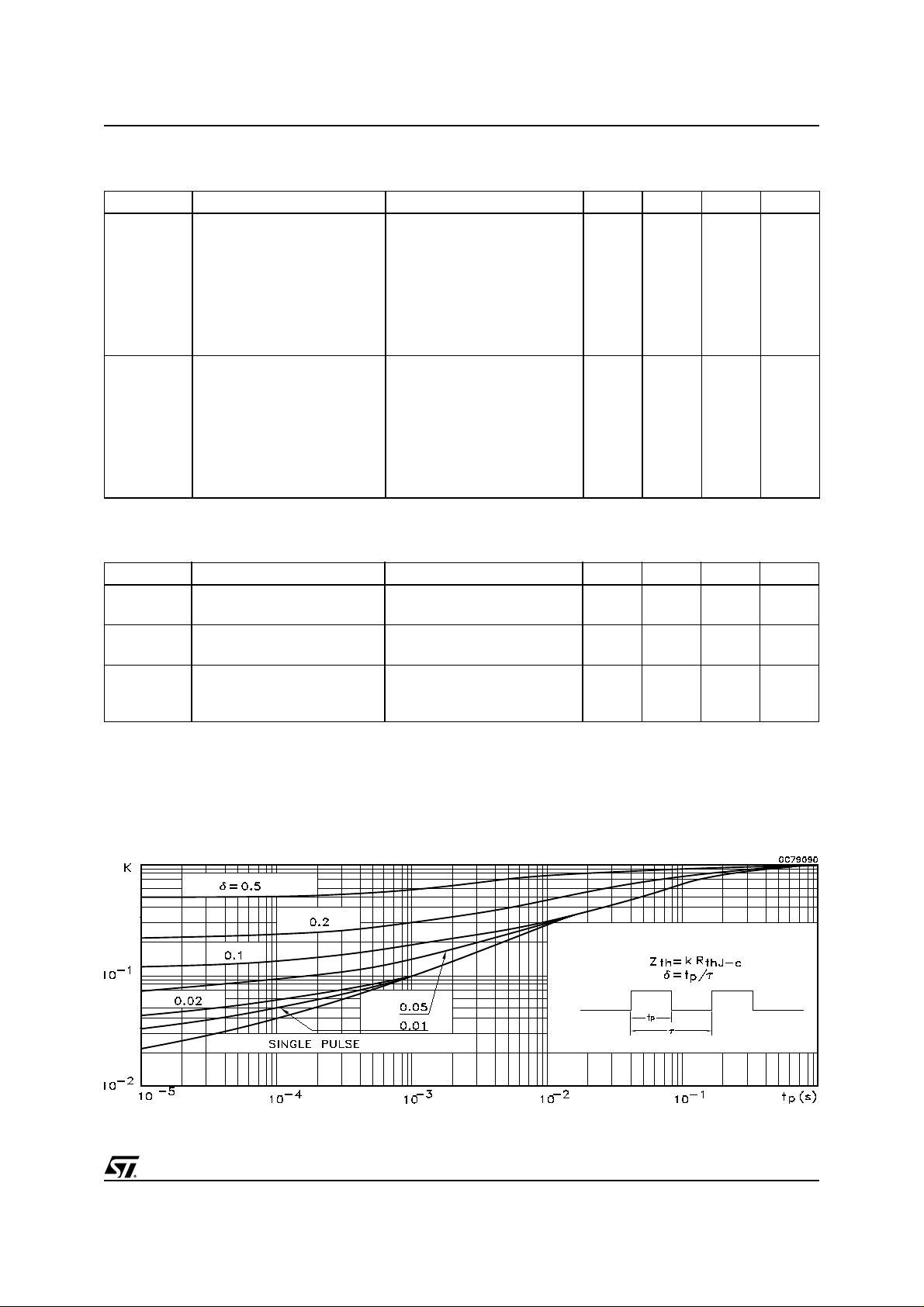
hermal Impedance
3/9
 Loading...