

SLLIMM™-nano (small low-loss intelligent molded module)
IPM, 3 A - 600 V 3-phase IGBT inverter bridge
Features
■ IPM 3 A, 600 V, 3-phase IGBT inverter bridge
including control ICs for gate driving and
freewheeling diodes
■ Optimized for low electromagnetic interference
■ V
■ 3.3 V, 5 V, 15 V CMOS/TTL input comparators
with hysteresis and pull-down resistor
■ Undervoltage lockout
■ Internal bootstrap diode
■ Interlocking function
■ Optimized pinout for easy board layout
negative temperature coefficient
CE(sat)
STGIPN3H60A
Datasheet − production data
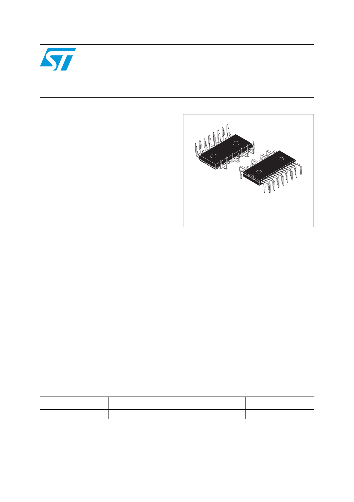
NDIP-26L
Applications
■ 3-phase inverters for motor drives
■ Dish washers, refrigerator compressors,
heating systems, air-conditioning fans,
draining and recirculation pumps
Table 1. Device summary
Order code Marking Package Packaging
Description
This intelligent power module implements a
compact, high-performance AC motor drive in a
simple, rugged design. It is composed of six
IGBTs with freewheeling diodes and three halfbridge HVICs for gate driving, providing low
electromagnetic interference (EMI) characteristics
with optimized switching speed. The package is
optimized for thermal performance and
compactness in built-in motor applications, or
other low power applications where assembly
space is limited. SLLIMM™ is a trademark of
STMicroelectronics.
STGIPN3H60A GIPN3H60A NDIP-26L Tube
May 2012 Doc ID 018958 Rev 3 1/17
This is information on a product in full production.
www.st.com
17

Contents STGIPN3H60A
Contents
1 Internal schematic diagram and pin configuration . . . . . . . . . . . . . . . . 3
2 Electrical ratings . . . . . . . . . . . . . . . . . . . . . . . . . . . . . . . . . . . . . . . . . . . . 6
2.1 Absolute maximum ratings . . . . . . . . . . . . . . . . . . . . . . . . . . . . . . . . . . . . . 6
2.2 Thermal data . . . . . . . . . . . . . . . . . . . . . . . . . . . . . . . . . . . . . . . . . . . . . . . 7
3 Electrical characteristics . . . . . . . . . . . . . . . . . . . . . . . . . . . . . . . . . . . . . 8
3.1 Control part . . . . . . . . . . . . . . . . . . . . . . . . . . . . . . . . . . . . . . . . . . . . . . . . 9
4 Application information . . . . . . . . . . . . . . . . . . . . . . . . . . . . . . . . . . . . . 11
4.1 Recommendations . . . . . . . . . . . . . . . . . . . . . . . . . . . . . . . . . . . . . . . . . . 12
5 Package mechanical data . . . . . . . . . . . . . . . . . . . . . . . . . . . . . . . . . . . . 13
6 Revision history . . . . . . . . . . . . . . . . . . . . . . . . . . . . . . . . . . . . . . . . . . . 16
2/17 Doc ID 018958 Rev 3
STGIPN3H60A Internal schematic diagram and pin configuration
V
V
V
1 Internal schematic diagram and pin configuration
Figure 1. Internal schematic diagram
Pin 1
GND
NC
cc W
HIN W
LIN W
NC
NC
NC
cc V
HIN V
GND
VCC
HIN
LIN VBOOT
GND
VCC
HIN
LIN VBOOT
HVG
OUT
LVG
HVG
OUT
LVG
Pin 26
N W
W, O UT W
Vboot W
N V
V, OUT V
LIN V
NC
cc U
HIN U
NC
LIN U
GND
VCC
HIN
LIN VBOOT
Pin 16
HVG
OUT
LVG
AM09917v1
Vboot V
N U
U,OUT U
P
Vboot U
Pin 17
Doc ID 018958 Rev 3 3/17

Internal schematic diagram and pin configuration STGIPN3H60A
Table 2. Pin description
Pin Symbol Description
1 GND Ground
2 NC Not connected
3V
W Low voltage power supply W phase
CC
4 HIN W High side logic input for W phase
5 LIN W Low side logic input for W phase
6 NC Not connected
7 NC Not connected
8 NC Not connected
9V
V Low voltage power supply V phase
CC
10 HIN V High side logic input for V phase
11 LIN V Low side logic input for V phase
12 NC Not connected
13 V
U Low voltage power supply for U phase
CC
14 HIN U High side logic input for U phase
15 NC Not connected
16 LIN U Low side logic input for U phase
17 V
U Bootstrap voltage for U phase
boot
18 P Positive DC input
19 U U phase output
20 N
21 V
boot
U
V Bootstrap voltage for V phase
Negative DC input for U phase
22 V V phase output
23 N
24 V
boot
V
W Bootstrap voltage for W phase
Negative DC input for V phase
25 W W phase output
26 N
W
Negative DC input for W phase
4/17 Doc ID 018958 Rev 3
STGIPN3H60A Internal schematic diagram and pin configuration
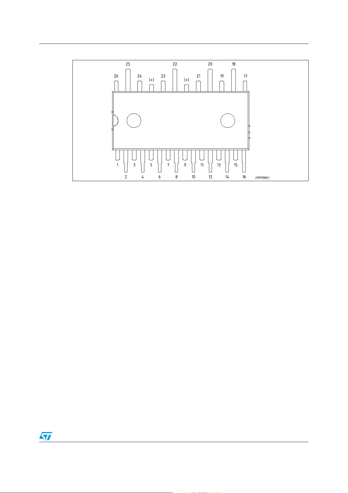
Figure 2. Pin layout (top view)
(*) Dummy pin internally connected to P (positive DC input).
Doc ID 018958 Rev 3 5/17
Electrical ratings STGIPN3H60A
2 Electrical ratings
2.1 Absolute maximum ratings
Table 3. Inverter part
Symbol Parameter Value Unit
V
CES
± I
C
± I
CP
P
TOT
1. Applied between HIN
2. Calculated according to the iterative formula:
3. Pulse width limited by max junction temperature.
Each IGBT collector emitter voltage (V
Each IGBT continuous collector current at
(2)
(3)
= 25 °C
T
C
Each IGBT pulsed collector current 18 A
Each IGBT total dissipation at TC = 25 °C 8 W
, LINi and GND for i = U, V, W.
i
ICTC()
------------ ------------- ------------- ------------ ------------- ------------- ------------- ------------ --=
R
thj c–
V
(1)
= 0)
IN
–
T
jmax()TC
CE sat()max()Tjmax()ICTC
600 V
3A
(),()×
Table 4. Control part
Symbol Parameter Min. Max. Unit
Output voltage applied between OUTU, OUTV,
- GND
OUT
W
V
boot
-18 V
+ 0.3 V
boot
Low voltage power supply - 0.3 18 V
Bootstrap voltage - 0.3 618 V
Logic input voltage applied between HINi, LIN
and GND for i = U, V, W
i
- 0.3 V
+ 0.3 V
CC
Allowed output slew rate 50 V/ns
ΔV
V
OUT
V
CC
V
boot
V
IN
OUT/dT
Table 5. Total system
Symbol Parameter Value Unit
V
ISO
T
J
T
C
Isolation withstand voltage applied between each
pin and heatsink plate (AC voltage, t = 60 sec.)
1000 V
Power chips operating junction temperature -40 to 150 °C
Module case operating temperature -40 to 125 °C
6/17 Doc ID 018958 Rev 3
 Loading...