

ST STGIPL20K60 User Manual

SLLIMM™ (small low-loss intelligent molded module)
IPM, 3-phase inverter - 20 A, 600 V short-circuit rugged IGBT
Features
■ IPM 20 A, 600 V 3-phase IGBT inverter bridge
including control ICs for gate driving and freewheeling diodes
■ Short-circuit rugged IGBTs
■ V
■ 3.3 V, 5 V, 15 V CMOS/TTL inputs
comparators with hysteresis and pull down/pull
up resistors
■ Undervoltage lockout
■ Internal bootstrap diode
■ Interlocking function
■ Smart shutdown function
■ Comparator for fault protection against
overtemperature and overcurrent
■ Op amps for advanced current sensing
■ DBC substrate leading to low thermal
resistance
■ Isolation rating of 2500 V
■ 5 kΩ NTC for temperature control
Applications
negative temperature coefficient
CE(sat)
rms
/min
STGIPL20K60
SDIP-38L
AM01193v1
Description
This intelligent power module provides a compact,
high performance AC motor drive in a simple,
rugged design. Combining ST proprietary control
ICs with the most advanced short-circuit-rugged
IGBT system technology, this device is ideal for 3phase inverters in applications such as home
appliances and air conditioners. SLLIMM™ is a
trademark of STMicroelectronics.
■ 3-phase inverters for motor drives
■ Home appliances, such as washing machines,
refrigerators, air conditioners and sewing
machines
Table 1. Device summary
Order code Marking Package Packaging
STGIPL20K60 GIPL20K60 SDIP-38L Tube
June 2011 Doc ID 018946 Rev 1 1/22
www.st.com
22

Contents STGIPL20K60
Contents
1 Internal schematic diagram and pin configuration . . . . . . . . . . . . . . . . 3
2 Electrical ratings . . . . . . . . . . . . . . . . . . . . . . . . . . . . . . . . . . . . . . . . . . . . 6
2.1 Absolute maximum ratings . . . . . . . . . . . . . . . . . . . . . . . . . . . . . . . . . . . . . 6
2.2 Thermal data . . . . . . . . . . . . . . . . . . . . . . . . . . . . . . . . . . . . . . . . . . . . . . . 7
3 Electrical characteristics . . . . . . . . . . . . . . . . . . . . . . . . . . . . . . . . . . . . . 8
3.1 Control part . . . . . . . . . . . . . . . . . . . . . . . . . . . . . . . . . . . . . . . . . . . . . . . 10
3.1.1 NTC thermistor . . . . . . . . . . . . . . . . . . . . . . . . . . . . . . . . . . . . . . . . . . . 13
3.2 Waveform definitions . . . . . . . . . . . . . . . . . . . . . . . . . . . . . . . . . . . . . . . . 14
4 Smart shutdown function . . . . . . . . . . . . . . . . . . . . . . . . . . . . . . . . . . . . 15
5 Application information . . . . . . . . . . . . . . . . . . . . . . . . . . . . . . . . . . . . . 16
5.1 Recommendations . . . . . . . . . . . . . . . . . . . . . . . . . . . . . . . . . . . . . . . . . . 17
6 Package mechanical data . . . . . . . . . . . . . . . . . . . . . . . . . . . . . . . . . . . . 18
7 Revision history . . . . . . . . . . . . . . . . . . . . . . . . . . . . . . . . . . . . . . . . . . . 21
2/22 Doc ID 018946 Rev 1
STGIPL20K60 Internal schematic diagram and pin configuration
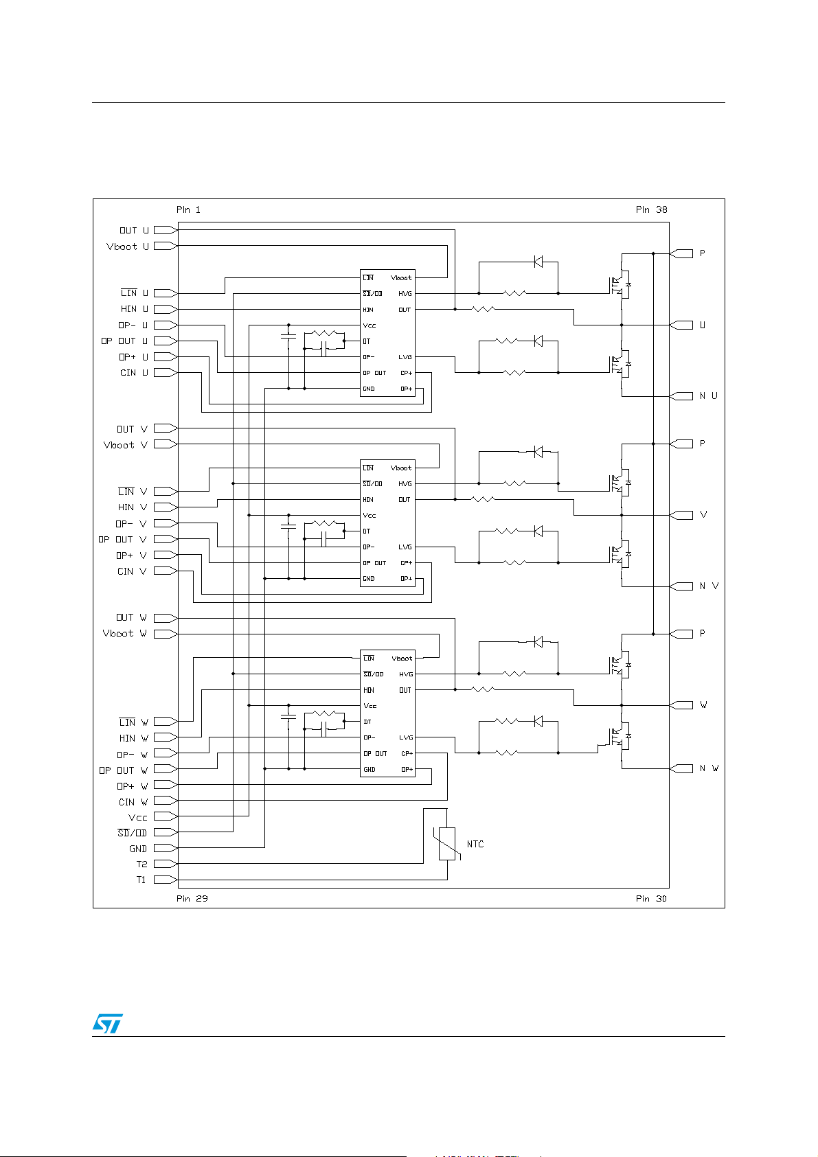
1 Internal schematic diagram and pin configuration
Figure 1. Internal schematic diagram
Doc ID 018946 Rev 1 3/22

Internal schematic diagram and pin configuration STGIPL20K60
Table 2. Pin description
Pin Symbol Description
1OUT
2V
3LIN
4HIN
5OP-
6OP
boot U
U
U
U
OUT U
7OP+
8CIN
U
9OUT
10 V
11 LIN
12 HIN
13 OP-
14 OP
boot V
V
V
V
OUT V
15 OP+
16 CIN
17 OUT
18 V
19 LIN
20 HIN
21 OP-
22 OP
23 OP+
24 CIN
25 V
26 SD
V
W
boot W
W
W
W
OUT W
W
W
CC
/ OD Shutdown logic input (active low) / open drain (comparator output)
High side reference output for U phase
U
Bootstrap voltage for U phase
Low side logic input for U phase
High side logic input for U phase
Op amp inverting input for U phase
Op amp output for U phase
Op amp non inverting input for U phase
U
Comparator input for U phase
High side reference output for V phase
V
Bootstrap voltage for V phase
Low side logic input for V phase
High side logic input for V phase
Op amp inverting input for V phase
Op amp output for V phase
Op amp non inverting input for V phase
V
Comparator input for V phase
High side reference output for W phase
Bootstrap voltage for W phase
Low side logic input for W phase
High side logic input for W phase
Op amp inverting input for W phase
Op amp output for W phase
Op amp non inverting input for W phase
Comparator input for W phase
Low voltage power supply
27 GND Ground
28 T
29 T
30 N
2
1
W
NTC thermistor terminal 2
NTC thermistor terminal 1
Negative DC input for W phase
31 W W phase output
32 P Positive DC input
33 N
V
Negative DC input for V phase
34 V V phase output
35 P Positive DC input
4/22 Doc ID 018946 Rev 1
STGIPL20K60 Internal schematic diagram and pin configuration
Table 2. Pin description (continued)
Pin Symbol Description
36 N
U
Negative DC input for U phase
37 U U phase output
38 P Positive DC input
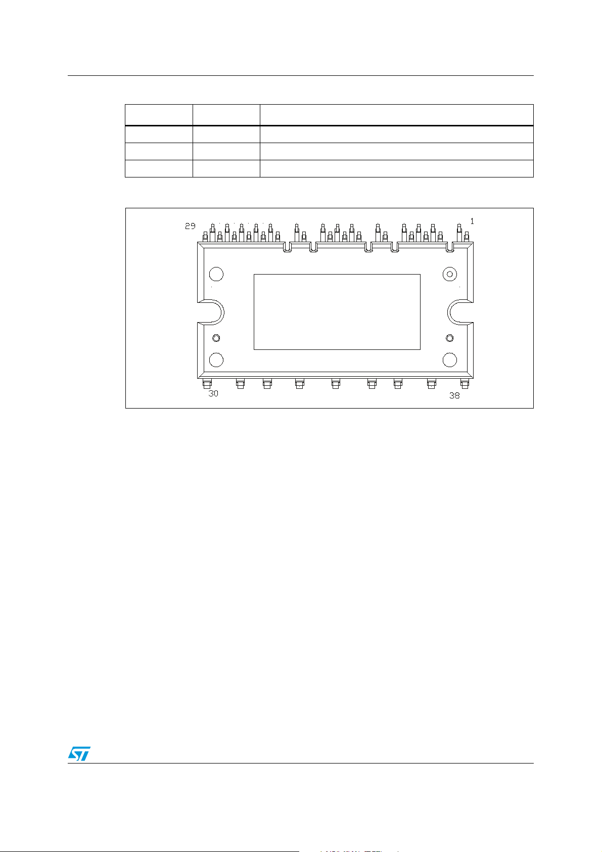
Figure 2. Pin layout (bottom view)
Marking area
Doc ID 018946 Rev 1 5/22

Electrical ratings STGIPL20K60
2 Electrical ratings
2.1 Absolute maximum ratings
Table 3. Inverter part
Symbol Parameter Value Unit
V
V
PN(surge)
V
CES
± I
± I
CP
P
TOT
t
scw
1. Applied between HINi, LINi and GND for i = U, V, W
2. Calculated according to the iterative formula:
3. Pulse width limited by max junction temperature
Supply voltage applied between P-NU, NV, N
PN
W
Supply voltage (surge) applied between P-NU, NV,
N
W
Each IGBT collector emitter voltage (V
Each IGBT continuous collector current
(2)
C
(3)
= 25 °C
at T
C
Each IGBT pulsed collector current 40 A
(1)
= 0)
IN
450 V
500 V
600 V
20 A
Each IGBT total dissipation at TC = 25 °C 56 W
Short circuit withstand time, VCE = 0.5 V
Tj = 125 °C, VCC = V
ICTC()
boot
-------------------------------------------------------------------------------------------------------=
R
= 15 V, V
thj c–
(1)
IN
T
V
CE sat()max()Tjmax()ICTC
= 0 - 5 V
jmax()TC
(BR)CES
–
5µs
(),()×
Table 4. Control part
Symbol Parameter Value Unit
V
OUT
V
V
CIN
V
boot
V
V
SD/OD
dV
out
Output voltage applied between OUTU, OUTV,
- GND (VCC = 15 V)
OUT
W
Low voltage power supply -0.3 to +21 V
CC
Comparator input voltage -0.3 to VCC +0.3 V
Bootstrap voltage applied between V
for i = U, V, W
Logic input voltage applied between HIN, LIN and
IN
GND
Open drain voltage -0.3 to 15 V
/dt Allowed output slew rate 50 V/ns
6/22 Doc ID 018946 Rev 1
boot i
- OUTi
- 21 to V
V
boot
boot
-0,3 to 620 V
-0.3 to 15 V
+ 0.3 V
STGIPL20K60 Electrical ratings
Table 5. Total system
Symbol Parameter Value Unit
V
ISO
(1)
T
j
T
C
Isolation withstand voltage applied between each
pin and heatsink plate (AC voltage, t = 60 sec.)
Operating junction temperature -40 to 150 °C
Module case operation temperature -40 to 125 °C
1. The maximum junction temperature rating of the power chips integrated within the SDIP module is 150°C
(@T
≤ 100°C). To ensure safe operation of the SDIP module, the average junction temperature should be
C
limited to T
≤ 125°C (@TC ≤ 100°C)
j(avg)
2.2 Thermal data
Table 6. Thermal data
Symbol Parameter Value Unit
R
thJC
Thermal resistance junction-case single IGBT 2.2 °C/W
Thermal resistance junction-case single diode 4.5 °C/W
2500 V
Doc ID 018946 Rev 1 7/22
 Loading...