

查询STGF20NB60S供应商
STGF20NB60S
N-CHANNEL 13A - 600V TO-220FP
PowerMESH™ IGBT
Table 1: Ge neral Features
TYPE V
STGF20NB60S 600 V < 1.7 V 13 A
LOW ON-VOLTAGE DROP (V
HIGHT CURRENT CAPABILITY
OFF LOSSES INCLUDE TAIL CURRENT
HIGH INPUT IMPEDANCE (VOLTAGE
CESVCE(sat)
(Max)
@25°C
cesat
)
I
C
@100°C
DRIVEN)
DESCRIPTION
Using the latest high voltage technology based on
a patented strip layout, STMicroelectronics has
designed an advanced family of IGBTs, the PowerMESH
™
IGBTs, with outstanding performances.
The suffix “S” identifies a family optimized to
achieve minimum on-voltage drop for low frequency to applications (<1kHz).
APPLICATIONS
LIGHT DIMMER
STATIC RELAYS
MOTOR CONTROL
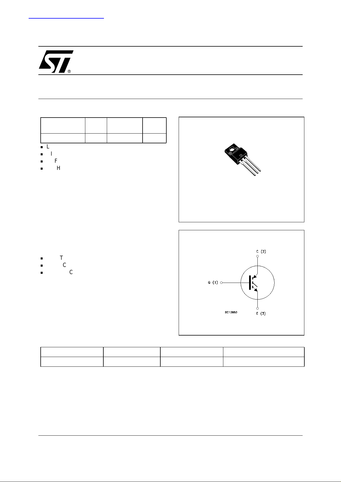
Figure 1: Package
3
2
1
TO-220FP
Figure 2: Internal Schematic Diagram
Table 2: Order Code
PART NUMBER MARKING PACKAGE PACKAGING
STGF20NB60S GF20NB60S TO-220FP TUBE
Rev. 2
1/10February 2005
STGF20NB60S
Table 3: Absolute Maximum ratings
Symbol Parameter Value Unit
V
CES
V
ECR
V
I
I
I
CM
P
TOT
V
T
() Pulse width limited by safe operating area
Table 4: Thermal Data
Rthj-case Thermal Resistance Junction-case 3.15 °C/W
Rthj-amb Thermal Resistance Junction-ambient 62.5 °C/W
Collector-Emitter Voltage (VGS = 0)
600 V
Emitter-Collector Voltage 20 V
Gate-Emitter Voltage ±20 V
GE
Collector Current (continuous) at TC = 25°C (#)
C
Collector Current (continuous) at TC = 100°C (#)
C
()
Collector Current (pulsed) 70 A
Total Dissipation at TC = 25°C
24 A
13 A
40 W
Derating Factor 0.32 W/°C
Insulation withstand voltage AC (t=1sec, Tc=25°C) 2500 V
ISO
Storage Temperature
stg
T
Operating Junction Temperature range
j
–55 to 150 °C
Min. Typ. Max.
T
L
Maximum Lead Temperature for Soldering Purpose (1.6 mm
300 °C
from case, for 10 sec.)
ELECTRICAL CHARACTERISTICS (T
=25°C UNLESS OTHERWISE SPECIFIED)
CASE
Table 5: On/Off
Symbol Parameter Test Conditions Min. Typ. Max. Unit
V
BR(CES)
Collector-Emitter Breakdown
Voltage
V
BR(ECS)
Emitter-Collector Breakdown
Voltage
I
CES
I
GES
V
GE(th)
V
CE(sat)
Collector cut-off Current
= 0)
(V
GE
Gate-Emitter Leakage
Current (V
CE
= 0)
Gate Threshold Voltage
Collector-Em itter Satur ation
Voltage
(#) Calculated according to the iterative formula:
T
–
ICTC()
--------------------------------------------------------------------------------------------------
=
R
THJ C–
JMAXTC
V
CESAT MAX()TCIC
,()×
IC = 250 µA, VGE = 0 600 V
IC = 1mA, VGE = 0 20 V
V
= Max Rating, TC = 25 °C
CE
VCE = Max Rating, TC = 125 °C
V
= ± 20V , VCE = 0 ±100 nA
GE
V
= VGE, IC = 250 µA
CE
VGE = 15V, IC = 20 A, Tj= 25°C
V
= 15V, IC = 20A, Tj=150°C
GE
2.5 5 V
1.25
1.2
10
100
1.7 V
µA
µA
V
2/10
STGF20NB60S
ELECTRICAL CHARACTERISTICS (CONTINUED)
Table 6: Dynamic
Symbol Parameter Test Conditions Min. Typ. Max. Unit
(1)
g
fs
C
ies
C
oes
C
res
Forward Transconductance
Input Capacitance
Output Capacitance 167 pF
Reverse Transfer
Capacitance
Q
g
Q
ge
Q
gc
I
CL
Total Gate Charge
Gate-Emitter Charge
Gate-Collector Charge
Turn-off SOA minimum
current
(1) Pulsed: Pulse durati on= 300 µs, dut y c yc l e 1.5%
Table 7: Switching On
Symbol Parameter Test Conditions Min. Typ. Max. Unit
t
d(on)
t
(di/dt)
t
d(on)
t
(di/dt)
r
r
Turn-on Delay Time
Current Rise Time
Turn-on Current Slope
on
Turn-on Delay Time
Current Rise Time
Turn-on Delay Time
on
VCE = 10 V , IC= 8 A 20 S
V
= 25 V, f= 1 MHz, VGE = 0
CE
1820 pF
27 pF
= 480 V, IC = 20 A,
V
CC
V
= 15 V
GE
(see Figure 19)
V
= 480 V , Tj = 125°C
clamp
80 A
83
10
27
115 nC
RG = 100 Ω
VCC = 480 V, IC = 20 A
RG= 100 Ω, VGE= 15V
(see Figure 17)
= 480 V, IC = 20 A
V
CC
RG= 100 Ω, VGE= 15V,
Tj= 125°C (see Figure 17)
92
70
340
80
73
320
nC
nC
ns
ns
A/µs
ns
ns
A/µs
Table 8: Switching Off
Symbol Paramet er Test Conditions Min. Typ. Max. Unit
V
= 480 V, IC = 20 A,
cc
RG = 100 Ω , VGE = 15 V
T
= 25 °C
J
(see Figure 17)
V
= 480 V, IC = 20 A,
cc
R
= 100 Ω , VGE = 15 V
G
Tj = 125 °C
(see Figure 17)
1.6 µs
2.4 µs
µs
t
r(Voff
td(
t
r(Voff
t
d(off
t
c
off
t
f
t
c
t
f
Cross-over Time
)
Off Voltage Rise Time 0.78 µs
)
Turn-off Delay Time 1.1 µs
Current Fall Time 0.79 µs
Cross-over Time
)
Off Voltage Rise Time 1.1 µs
)
Turn-off Delay Time 2.4 µs
Current Fall Time 1.2
Table 9: Switching Energy
Symbol Parameterr Test Conditions Min. Typ. Max Unit
Eon
(2)
Turn-on Switching Losses
E
off
E
ts
Eon (2)
E
off
E
ts
(2) Eon i s t he tur n-on l oss es wh en a typ ica l diod e is used in th e tes t cir cui t in fig ure 2. I f the IGB T is o ffere d in a pac kage w it h a co- pa ck
diode, the co-pack diode is used as exte rnal diode.
(3) Turn-off losses in clude also the tail of the collector current.
Turn-off Switching Loss
(3)
Total Switching Loss
Turn-on Switching Losses
Turn-off Switching Loss
(3)
Total Switching Loss
= 480 V, IC = 20 A
V
CC
RG= 100 Ω, VGE= 15V,
(see Figure 18)
= 480 V, IC = 20 A
V
CC
RG= 100 Ω, VGE=15V,Tj=125°C
(see Figure 18)
0.84
7.4
8.24
0.86
11.5
12.4
mJ
mJ
mJ
mJ
mJ
mJ
3/10
 Loading...