

1
3
1
3
3
查询STG3684A供应商
N-CHANNEL 10A - 600V - TO-220/TO-220FP/D2PAK
STGP10NC60KD - STGF10NC60KD
STGB10NC60KD
SHORT CIRCUIT RATED PowerMESH™ IGBT
Table 1: General Fe a ture s
TYPE V
STGB10NC60KD
STGF10NC60KD
STGP10NC60KD
■ LOWER ON-VOLTAGE DROP (V
■ OFF LOSSES INCLUDE TAIL CURRENT
■ LOWER C
■ SWITCHING LOSSES INCLUDE DIODE
RES
CESVCE(sat)
600 V
600 V
600 V
/ C
RATIO
IES
(Max)
@25°C
< 2.5 V
< 2.5 V
< 2.5 V
cesat
I
C
@100°C
10 A
6 A
10 A
)
RECOVERY ENERGY
■ VERY SOFT ULTRA FAST RECOVERY
ANTIPARALLEL DIODE
■ NEW GENERATION PRODUCTS WITH
TIGHTER PARAMETER DISTRUBUTION
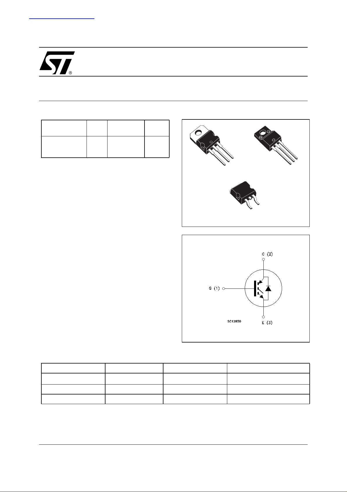
DESCRIPTION
Using the latest high voltage technology based on
a patented strip layout, STMicroelectronics has
designed an advanced family of IGBTs, the Pow
erMESH™ IGBTs, with outstanding performances.
The suffix “K” identifies a family optimized for high
frequency motor control applications with short cir
cuit withstand capab ilit y.
Figure 1: Package
2
TO-220FPTO-220
1
D²PAK
Figure 2: Internal Schematic Diagram
2
APPLICATIONS
■ HIGH FREQUENCY MOTOR CONTROLS
■ SMPS and PFC IN BOTH HARD SWITCH AND
RESONANT TOPOLOGIES
■ MOTOR DRIVERS
Table 2: Order Codes
SALES TYPE MARKING PACKAGE PACKAGING
STGB10NC60KDT4 GB10NC60KD
STGF10NC60KD GF10NC60KD TO-220FP TUBE
STGP10NC60KD GP10NC60KD TO-220 TUBE
D²PAK
TAPE & REEL
Rev. 2
1/14July 2005
STGP10NC60KD - STGB10NC60KD - STGF10NC60KD
Table 3: Absolute Maximum ratings
Symbol Parameter Value Unit
I
V
V
V
CM
P
CES
ECR
I
I
TOT
I
Collector-Emitter Voltage (VGS = 0)
Emitter-Collector Voltage 20 V
Gate-Emitter Voltage ±20 V
GE
Collector Current (continuous) at TC = 25°C (#)
C
Collector Current (continuous) at TC = 100°C (#)
C
()
Collector Current (pulsed) 40 A
Diode RMS Forward Current at TC = 25°C
F
Total Dissipation at TC = 25°C
Derating Factor 0.48 0.20 W/°C
V
T
()Pulse wi dth limited by max. jun ct i on temperature.
ISO
stg
T
Insulation Withstand Voltage A.C.(t = 1 sec; Tc = 25°C) -- 2500 V
Storage Temperature
Operating Junction Temperature
j
STGB10NC60KD
STGP10NC60KD
20 9 A
10 6 A
60 25 W
STGF10NC60KD
600 V
10 A
– 55 to 150 °C
Table 4: Thermal Data
Min. Typ. Max.
Rthj-case Thermal Resistance Junctio n-cas e TO-220
D2PAK
2.08 °C/W
TO-220FP 5.0 °C/W
Rthj-amb Thermal Resistance Junctio n-amb ient 62.5 °C/W
T
Maximum Lead Temperature for Soldering
L
300 °C
Purpose (1.6 mm from case, for 10 sec.)
ELECTRICAL CHARACTERISTICS (T
=25°C UNLESS OTHERWISE SPECIFIED)
CASE
Table 5: Main Parameters
Symbol Parameter Test Conditions Min. Typ. Max. Unit
V
BR(CES)
I
CES
I
GES
V
GE(th)
V
CE(sat)
(#) Calculated according to the iterative formula:
Collector-Emitter
Breakdown Voltage
Collector cut-off Current
(VGE = 0)
Gate-Emitter Leakage
Current (VCE = 0)
Gate Threshold Voltage
Collector-Emitter
Saturation Voltage
IC= 1 mA, VGE= 0 600 V
VCE= Max Rating,
10
TC= 25°C
VCE=Max Rating,
1
TC= 125°C
VGE= ±20V , VCE= 0 ±100 nA
VCE= VGE, IC= 250 µA
VGE= 15V, IC= 5A
VGE= 15V, IC= 5A,
5 7 V
2
2.5 V
1.8
Tc= 125°C
µA
mA
V
2/14
ICT
()
T
–
--------------------------------------------------------------------------------------------------
=
C
R
THJ C–
JMAXTC
V
CESAT MAX()TCIC
,()×
STGP10NC60KD - STGB10NC60KD - STGF10NC60KD
ELECTRICAL CHARACTERISTICS (CONTINUED)
Table 6: Dynamic
Symbol Parameter Test Conditions Min. Typ. Max. Unit
gfs(1)
C
ies
C
oes
C
res
Q
g
Q
ge
Q
gc
t
scw
Forward Transconductance
Input Capacitance
Output Capacitance
Reverse Transfer
Capacitance
Total Gate Charge
Gate-Emitter Charge
Gate-Collector Charge
Short Circuit Withstand Time VCE = 0.5 V
Table 7: Switching On
Symbol Parameter Test Conditions Min. Typ. Max. Unit
t
d(on)
t
(di/dt)
t
d(on)
t
(di/dt)
r
r
Turn-on Delay Time
Current Rise Time
Turn-on Current Slope
on
Turn-on Delay Time
Current Rise Time
Turn-on Current Slope
on
VCE = 15 V, IC= 5 A 15 S
VCE = 25V, f = 1 MHz, VGE = 0 380
46
8.5
VCE = 390 V, IC = 5 A,
VGE = 15V,
(see Figure 20)
, Tj = 125°C
BR(CES)
10 µs
19
5
9
RG = 10 Ω, VGE = 12V
VCC = 390 V, IC = 5 A
RG= 10Ω, VGE= 15V, Tj= 25°C
(see Figure 18)
VCC = 390 V, IC = 5 A
RG= 10Ω, VGE= 15V, Tj=125°C
(see Figure 18)
17
6
655
16.5
6.5
575
pF
pF
pF
nC
nC
nC
ns
ns
A/µs
ns
ns
A/µs
Table 8: Switching Off
Symbol Parameter Test Conditions Min. Typ. Max. Unit
tr(V
)
td(
off
off
t
f
Off Voltage Rise Time
Turn-off Delay Time
)
Current Fall Time
Vcc = 390 V, IC = 5 A,
RGE = 10 Ω , VGE = 15 V
TJ = 25 °C
33
72
82
ns
ns
ns
(see Figure 18)
tr(V
)
td(
off
off
t
f
Off Voltage Rise Time
Turn-off Delay Time
)
Current Fall Time
Vcc = 390 V, IC = 5 A,
RGE = 10 Ω , VGE = 15 V
Tj = 125 °C
60
106
136
ns
ns
ns
(see Figure 18)
Table 9: Switching Energy
Symbol Parameter Test Conditions Min. Typ. Max. Unit
Eon (2)
E
off
E
ts
Eon (2)
E
off
E
ts
(1) Pulsed: Pulse du ration = 300 µ s, duty cycl e 1.5%
(2) Eon is the turn-on losses when a typical diode is used in the test circuit in figure 2. If the IGBT is offered in a package with a co-pack diode,
the co-pack diode i s us ed as extern al di ode. IGBTs & DIODE are at the same tem perature (25°C and 125°C)
(3)Turn-off los ses include al so the tail of t he collector current.
Turn-on Switching Losses
Turn-off Switching Losses
(3)
Total Switching Losses
Turn-on Switching Losses
Turn-off Switching Losses
(3)
Total Switching Losses
VCC = 390 V, IC = 75 A
RG= 10 Ω, VGE= 15V, Tj= 25°C
(see Figure 18)
VCC = 390 V, IC = 5 A
RG= 10 Ω, VGE= 15V, Tj= 125°C
(see Figure 18)
55
85
140
87
162
249
µJ
µJ
µJ
µJ
µJ
µJ
3/14

STGP10NC60KD - STGB10NC60KD - STGF10NC60KD
Table 10: Collector-Emitter Diode
Symbol Parameter Test Conditions Min. Typ. Max. Unit
V
f
t
rr
Q
rr
I
rrm
t
rr
Q
rr
I
rrm
Forward On-Voltage If = 2.5 A
If = 2.5 A, Tj = 125 °C
Reverse Recovery Time
Reverse Recovery Charge
Reverse Recovery Current
Reverse Recovery Time
Reverse Recovery Charge
Reverse Recovery Current
If = 5 A ,VR = 30 V,
Tj = 25°C, di/dt = 100 A/μs
(see Figure 6)
If = 5 A ,VR = 30 V,
Tj =125°C, di/dt = 100 A/μs
(see Figure 6)
1.6
1.3
23.5
16.5
1.4
39
39
2
2.1
V
V
ns
nC
A
ns
nC
A
4/14
STGP10NC60KD - STGB10NC60KD - STGF10NC60KD
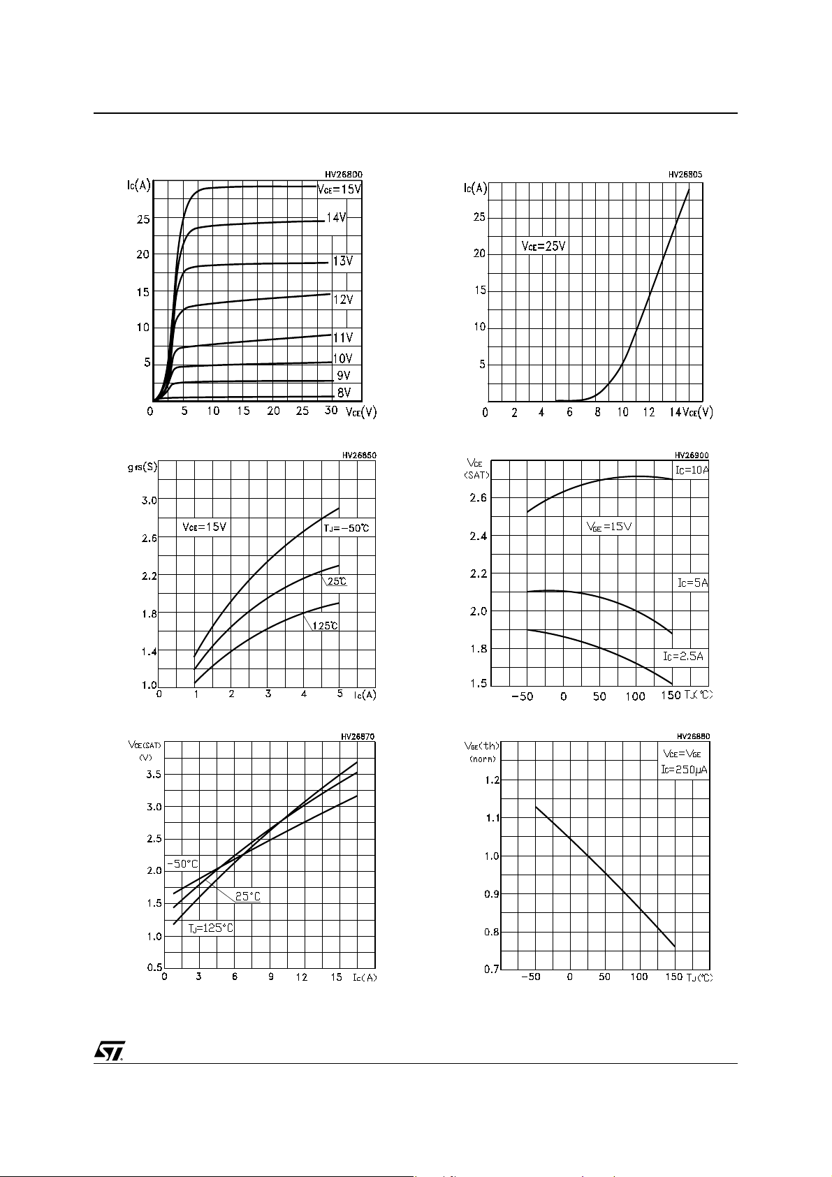
Figure 3: Output Characteristics
Figure 4: Transconductance
Figure 6: Transfer Characteristics
Figure 7: Collector-Emitter On Voltage vs Temperature
Figure 5: Collector-Emitter On Voltage vs Collector Current
Figure 8: Normalized Gate Threshold vs Temperature
5/14
 Loading...