

查询STGD7NB120S-1供应商
N-CHANNEL 7A - 1200V IPAK
TYPE V
CES
STGD7NB120S-1 1200 V < 2.1 V 7 A
■ HIGHINPUTIMPEDANCE
(VOLTAGEDRIVEN)
■ VERYLOW ON-VOLTAGEDROP (V
■ HIGHCURRENT CAPABILITY
■ OFFLOSSES INCLUDE TAIL CURRENT
DESCRIPTION
Using the latest high voltage technology based
on a patented strip layout, STMicroelectronics
has designed an advanced family of IGBTs, the
PowerMESH IGBTs, with outstanding
perfomances. The suffix ”S” identifies a family
optimized to achieve minimum on-voltage drop
for low frequencyapplications(<1kHz).
APPLICATIONS
■ LIGHT DIMMER
■ INRUSHCURRENT LIMITATION
■ MOTORCONTROL
V
CE(sat)
cesat
I
C
)
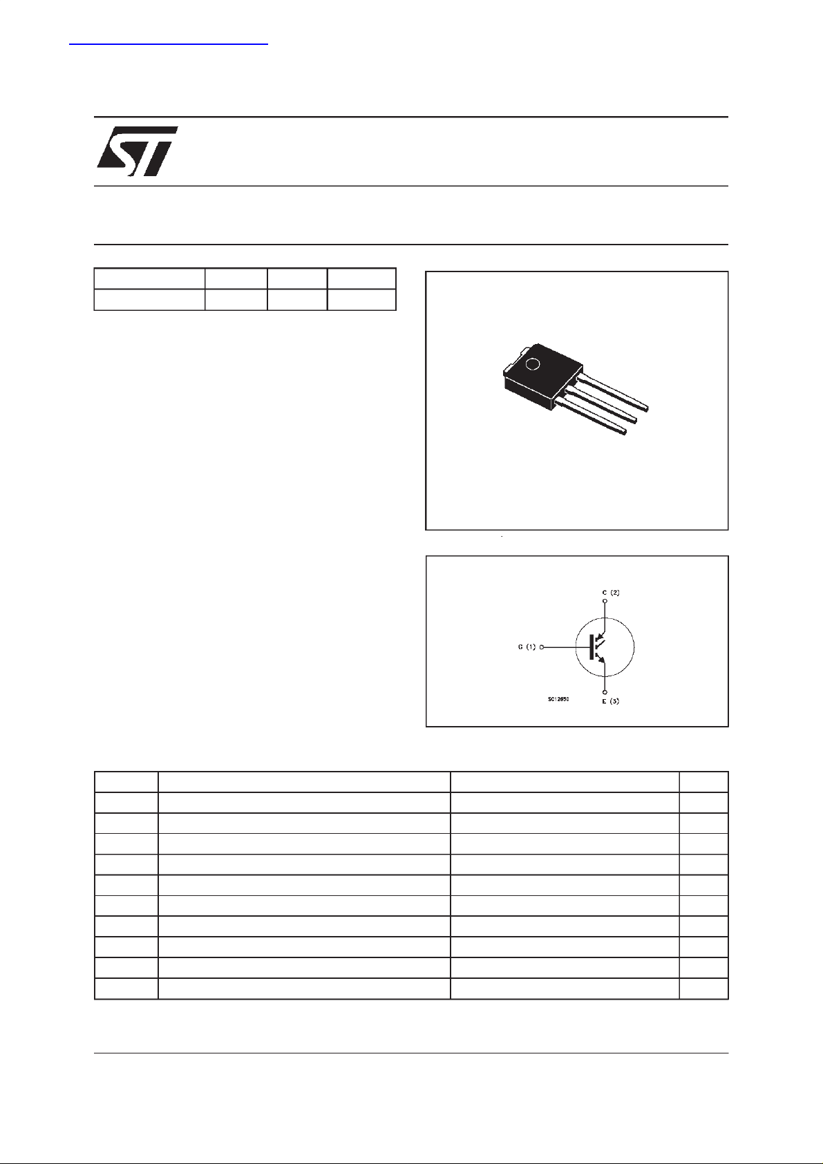
STGD7NB120S-1
Power MESH IGBT
PRELIMINARY DATA
3
2
1
IPAK
TO-251
(Suffix”-1”)
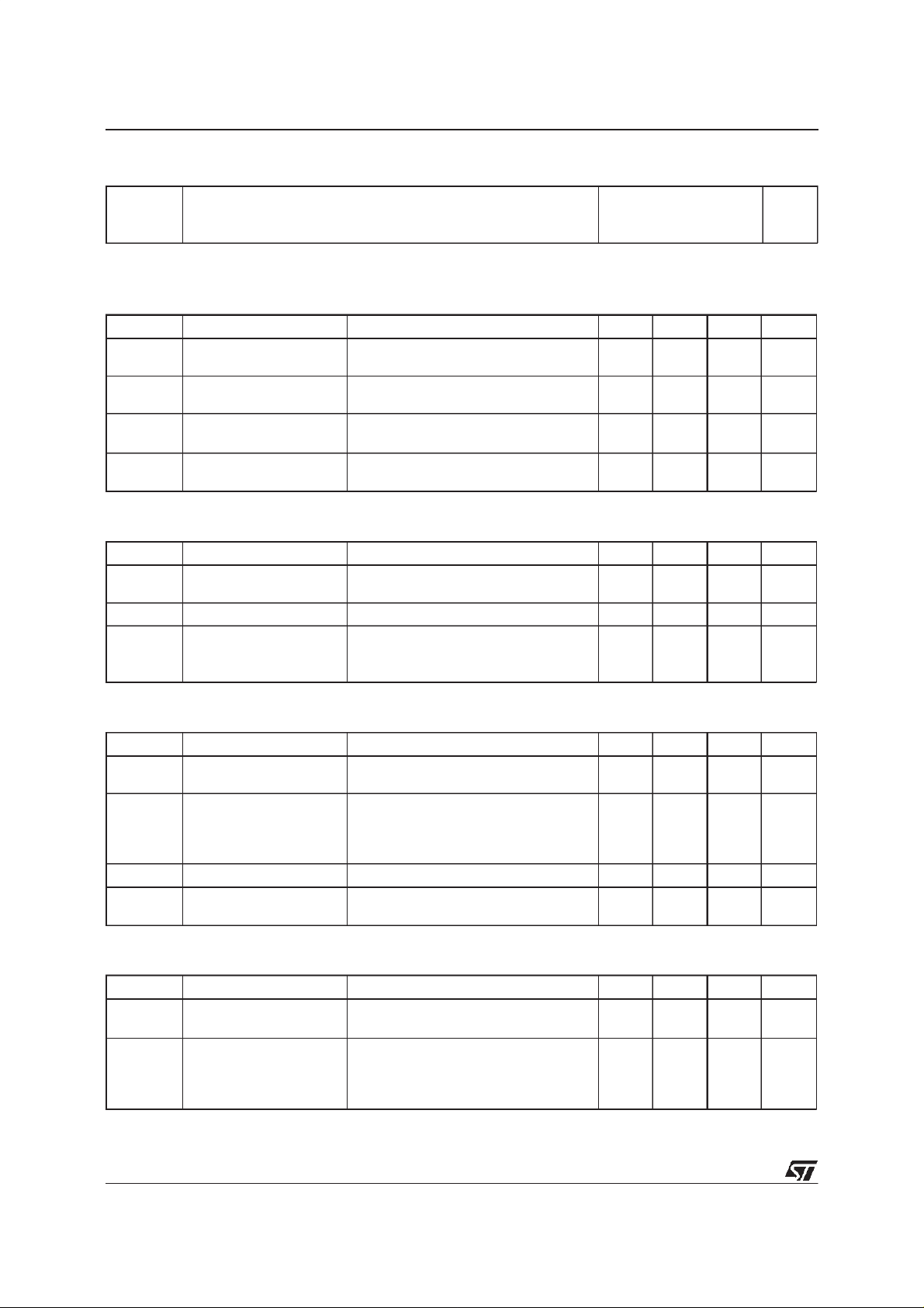
INTERNAL SCHEMATIC DIAGRAM
ABSOLUTE MAXIMUM RATINGS
Symb o l Parameter Value Unit
V
V
V
I
CM
P
T
(•) Pulse width limited by safe operating area
April 2000
Collect o r -Em i t t er Voltage ( VGS= 0) 1200 V
CES
Reverse Battery Protection 20 V
ECR
Gate-Emitter Voltage
GE
I
Collect o r Curr ent ( con t inuous) at Tc=25oC10A
C
I
Collect o r Curr ent ( con t inuous) at Tc= 100oC7A
C
20 V
±
(•) Collector Curr ent (pulsed) 20 A
Tot al Di s si pat ion at Tc=25oC55W
tot
Derat ing Factor 0.4 W/
Sto rage Tem perature -65 to 15 0
stg
T
Max. Operat ing Junc tion Tem per ature 150
j
o
C
o
C
o
C
1/6
STGD7NB120S-1
THERMAL DATA
R
thj-case
R
thj-amb
R
thc-sink
Ther mal Resistanc e Junct ion-case Max
Ther mal Resistanc e Junct ion-ambient Max
Ther mal Resistanc e Case-sink Ty p
2.27
100
1.5
o
C/W
o
C/W
o
C/W
ELECTRICAL CHARACTERISTICS
=25oC unless otherwisespecified)
(T
j
OFF
Symbol Parameter Test Conditions Min. Typ. Max. Unit
V
BR(CES)
Collector-Emitter
IC=250µAVGE= 0 1200 V
Break dow n Volt age
V
BR(ECR)
Emitter-Collector
IC = 10 mA VGE=0 20 V
Break dow n Volt age
I
I
CES
GES
Collect o r cut - off
=0)
(V
GE
Gat e- Em i t t er Lea k age
Current (V
CE
=0)
V
=MaxRating Tj=25oC
CE
=0.8MaxRating Tj= 125oC
V
CE
V
= ± 20 V VCE=0 ±100 nA
GE
250
1000
ON(∗)
Symbol Parameter Test Conditions Min. Typ. Max. Unit
V
GE(th)
Gate Threshold
VCE=VGEIC= 250 µ A35V
Voltage
V
V
CE(SAT)
Gat e Em it t er Volt age VCE=2.5V IC=2A Tj=25 ÷125oC6.5V
GE
Collector-Emitter
Sat urat ion Volt age
VGE=15V IC=3.5A
=15V IC=7A
V
GE
V
=15V IC=10A 1.7
GE
1.6
2.1
DYNAMIC
µ
µA
V
V
V
A
Symbol Parameter Test Conditions Min. Typ. Max. Unit
g
Forward
fs
VCE=25 V IC=7A 2.5 4.5 S
Tr ansc on duc tance
C
C
C
Input C apacitance
ies
Out put Capacitance
oes
Reverse Tr ansfer
res
VCE=25V f=1MHz VGE= 0 430
40
7
Capacit a nc e
Q
I
CL
Gat e Charge VCE= 960 V IC=7A VGE= 15 V 29 nC
G
Latc hing Curr ent V
=960V RG=1kΩ
clamp
= 150oC
T
j
10 A
SWITCHINGON
Symbol Parameter Test Conditions Min. Typ. Max. Unit
(di/dt)
2/6
t
d(on)
E
Delay Time
t
Rise Ti m e
r
Tur n-on Current Slope
on
Turn-on
on
Switching Losses
VCC= 960 V IC=7A
=15V RG=1KΩ
V
GE
VCC=960V IC=7A
=1KΩ VGE=15V
R
G
T
=125oC
j
570
270
800
3.2
pF
pF
pF
ns
ns
A/µs
mJ

STGD7NB120S-1
ELECTRICAL CHARACTERISTICS
(continued)
SWITCHINGOFF
Symbol Parameter Test Conditions Min. Typ. Max. Unit
t
tr(v
E
off
t
tr(v
E
off
(•) Pulse width limited by safe operating area
(∗) Pulsed: Pulse duration = 300 µs, duty cycle 1.5%
(**)Losses Include Also The Tail (JedecStandardization)
Cross-Over Time
c
Off Voltage Rise Time
)
off
Fall T ime
t
f
(**)
Turn-off Switching Loss
Cross-Over Time
c
Off Voltage Rise Time
)
off
Fall T ime
t
f
(**)
Turn-off Switching Loss
VCC=960V IC=7A
R
=1000
GE
V
=960V IC=7A
CC
=1000
R
GE
= 125oC
T
j
Ω
Ω
VGE=15V
VGE=15V
4.9
2.9
3.3
15
7.5
5.5
6.2
22
µs
µ
µs
mJ
µs
µ
µs
mJ
s
s
3/6

STGD7NB120S-1
SwitchingOff Safe Operatin Area
Fig. 1: Gate Charge test Circuit
Fig. 3: SwitchingWaveforms
Fig. 2: Test Circuit For Inductive Load Switching
4/6

TO-251 (IPAK) MECHANICAL DATA
STGD7NB120S-1
DIM.
mm inch
MIN. TYP. MAX. MIN. TYP. MAX.
A 2.2 2.4 0.086 0.094
A1 0.9 1.1 0.035 0.043
A3 0.7 1.3 0.027 0.051
B 0.64 0.9 0.025 0.031
B2 5.2 5.4 0.204 0.212
B3 0.85 0.033
B5 0.3 0.012
B6 0.95 0.037
C 0.45 0.6 0.017 0.023
C2 0.48 0.6 0.019 0.023
D 6 6.2 0.236 0.244
E 6.4 6.6 0.252 0.260
G 4.4 4.6 0.173 0.181
H 15.9 16.3 0.626 0.641
L 9 9.4 0.354 0.370
L1 0.8 1.2 0.031 0.047
L2 0.8 1 0.031 0.039
A
E
==
C2
L2
B2
==
H
C
A3
A1
B6
L
B
B5
G
==
D
B3
2
13
L1
0068771-E
5/6

STGD7NB120S-1
Information furnished is believed to be accurate and reliable. However, STMicroelectronics assumes no responsibility forthe consequences
of use of such information nor for any infringement of patents or other rights of third parties which may result from its use. No license is
granted by implicationor otherwise under any patent or patent rights of STMicroelectronics. Specification mentioned in this publication are
subject to change without notice. Thispublication supersedes and replaces all information previously supplied. STMicroelectronics products
are not authorized for use as critical components in life support devices or systems without express written approval of STMicroelectronics.
The ST logo is a trademarkof STMicroelectronics
2000 STMicroelectronics – Printed in Italy – All Rights Reserved
STMicroelectronics GROUP OF COMPANIES
Australia - Brazil - China - Finland - France - Germany - Hong Kong - India - Italy - Japan - Malaysia - Malta - Morocco -
Singapore - Spain - Sweden - Switzerland - United Kingdom - U.S.A.
http://www.st.com
6/6
 Loading...