

STGD6NC60HD
N-CHANNEL 6A - 600V DPAK
Very Fast PowerMESH™ IGBT
TARGET SPECIFICATION
Table 1: Ge neral Features
TYPE V
STGD6NC60HDT4 600 V < 2.5 V6 A
■ LOWER ON-VOLTAGE DROP (V
■ OFF LOSSES INCLUDE TAIL CURRENT
■ LOSSES INCLUDE DIODE RECOVERY
CES
V
CE(sat)
(Max) @25°C
cesat
I
C
@100°C
)
ENERGY
■ LOWER C
■ HIGH FREQUENCY OPERATION
■ VERY SOFT ULTRA FAST RECOVERY ANTI
RES/CIES
RATIO
PARALLEL DIODE
■ NEW GENERATION PRODUCTS WITH
TIGHTER PARAMETER DISTRIBUTION
DESCRIPTION
Using the latest high voltage technology based on
a patented strip layout, STMicroelectronics has
designed an advanced family of IGBTs, the PowerMESH
™
IGBTs, with outstanding performances.
The suffix "H" identifies a family optimized for high
frequency applications in order to achieve very
high switching performances (reduced tfall) mantaining a low voltage drop.
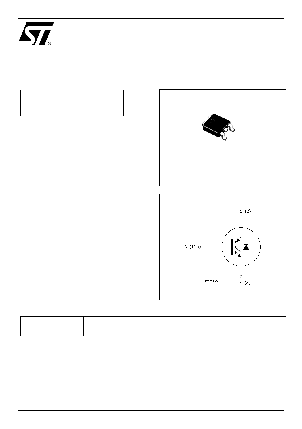
Figure 1: Package
3
1
DPAK
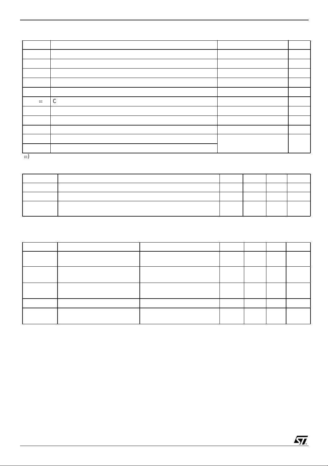
Figure 2: Internal Schematic Diagram
APPLICATIONS
■ HIGH FREQUENCY INVERTERS
■ SMPS AND PFC IN BOTH HARD SWITCH
AND RESONANT TOPOLOGIES
■ MOTOR DRIVERS
Table 2: Order Code
PART NUMBER MARKING PACKAGE PACKAGING
STGD6NC60HDT4 GD6NC60HD DPAK TAPE & REEL
June 2005
This is a preliminary information on a new product foreseen to be developed. Details are subjet to change without notice
Rev. 1
1/9
STGD6NC60HD
Table 3: Absolute Maximum ratings
Symbol Parameter Value Unit
V
CES
V
ECR
V
I
CM
P
TOT
T
() Pulse width limi ted by max. junction tempe rature.
Table 4: Thermal Data
Rthj-case Thermal Resistance Junction-case 2.5 °C/W
Rthj-amb Thermal Resistance Junction-ambient 100 °C/W
Collector-Emitter Voltage (VGS = 0)
600 V
Emitter-Collector Voltage 20 V
Gate-Emitter Voltage ±20 V
GE
I
Collector Current (continuous) at TC = 25°C (#)
C
I
Collector Current (continuous) at TC = 100°C (#)
C
()
Collector Current (pulsed) 24 A
Diode RMS Forward Current at TC = 25°C
I
F
Total Dissipation at TC = 25°C
10 A
6A
TBD A
50 W
Derating Factor 0.40 W/°C
Storage Temperature
stg
T
Operating Junction Temperature
j
– 55 to 150 °C
Min. Typ. Max.
T
L
Maximum Lead T emperature for Soldering Purpose (1.6 mm from
275 °C
case, for 10 sec.)
ELECTRICAL CHARACTERISTICS (T
=25°C UNLESS OTHERWISE SPECIFIED)
CASE
Table 5: Main Parameters
Symbol Parameter Test Conditions Min. Typ. Max. Unit
V
BR(CES)
Collector-Em itter Break down
Voltage
I
CES
I
GES
V
GE(th)
V
CE(sat)
Collector cut-off Current
= 0)
(V
GE
Gate-Emitter Leakage
Current (V
CE
= 0)
Gate Threshold Voltage
Collector-Em itter Satur ation
Voltage
(#) Calculated according to the iterative formula:
T
–
ICTC()
--------------------------------------------------------------------------------------------------
=
R
THJ C–
JMAXTC
V
CESAT MAX()TCIC
,()×
IC = 1 mA, VGE = 0 600 V
V
= Max Rating, TC = 25 °C
CE
VCE = Max Rating, TC = 125 °C
V
= ± 20V , VCE = 0 ±100 nA
GE
V
= VGE, IC = 250 µA
CE
VGE = 15V, IC = 3 A
VGE = 15V, IC = 3 A, Tc= 125 °C
3.75 5.75 V
1.9
1.7
10
1
2.5 V
µA
mA
V
2/9
STGD6NC60HD
ELECTRICAL CHARACTERISTICS (CONTINUED) Table 6: Dynamic
Symbol Parameter Test Conditions Min. Typ. Max. Unit
(1)
g
fs
C
ies
C
oes
C
res
Forward Transconductance
Input Capacitance
Output Capacitance 28 pF
Reverse Transfer
Capacitance
Q
g
Q
ge
Q
gc
I
CL
Total Gate Charge
Gate-Emitter Charge
Gate-Collector Charge
Turn-Off SOA Minimum
Current
(1) Pulsed: Pulse duration= 300 µs, duty cycle 1.5%
Table 7: Switching On
Symbol Parameter Test Conditions Min. Typ. Max. Unit
t
d(on)
t
(di/dt)
t
d(on)
t
(di/dt)
r
r
Turn-on Delay Time
Current Rise Time
Turn-on Current Slope
on
Turn-on Delay Time
Current Rise Time
Turn-on Current Slope
on
VCE = 15 V , IC= 3 A TBD S
V
= 25 V, f= 1 MHz, VGE = 0
CE
320 pF
7.2 pF
= 390 V, IC = 3 A,
V
CE
VGE = 15 V
(see Figure 5)
V
= 480 V , Tj = 150°C
clamp
R
= 10 Ω, VGE = 15 V
G
VCC = 390 V, IC = 3 A
R
=10 Ω, VGE= 15V, Tj= 25°C
G
(see Figure 3)
VCC = 390 V, IC = 3 A
RG=10 Ω, VGE= 15V , Tj= 125°C
(see Figure 3)
TBD A
15
TBD
TBD
TBD
TBD
TBD
TBD
TBD
TBD
TBD nC
nC
nC
ns
ns
A/µs
ns
ns
A/µs
Table 8: Switching Off
Symbol Paramet er Test Conditions Min. Typ. Max. Unit
t
r(Voff
t
d(off
t
r(Voff
t
d(off
)
Off Voltage Rise Time
)
Turn-off Delay Time TBD ns
t
f
t
f
Current Fall Time 70 ns
)
Off Voltage Rise Time
)
Turn-off Delay Time TBD ns
Current Fall Time TBD ns
Vcc = 390 V, IC = 3 A,
R
= 10 Ω , VGE = 15 V
G
TJ = 25 °C
(see Figure 3)
Vcc = 390 V, IC = 3 A,
R
= 10 Ω , VGE = 15 V
G
Tj = 125 °C
(see Figure 3)
TBD ns
TBD ns
Table 9: Switching Energy
Symbol Parameter Test Conditions Min. Typ. Max Unit
Eon (2)
E
off
E
ts
Eon (2)
E
off
E
ts
(2) Eon i s t he tur n-on l oss es wh en a typ ica l diod e is used in th e tes t cir cui t in fig ure 2. I f the IGB T is o ffere d in a pac kage w it h a co- pa ck
diode, the co-pack diode is used as external diode. IGBTs & DIODE are at the same temperature (25°C and 125°C)
(3) Turn-off losses include als o the tail of th e collector current.
Turn-on Switching Losses
Turn-off Switching Loss
(3)
Total Switching Loss
Turn-on Switching Losses
Turn-off Switching Loss
(3)
Total Switching Loss
= 390 V, IC = 3 A
V
CC
R
= 10 Ω, VGE= 15V, Tj= 25°C
G
(see Figure 3)
= 390 V, IC = 3 A
V
CC
RG= 10 Ω, VGE= 15V, Tj= 125°C
(see Figure 3)
TBD
TBD
TBD
TBD
TBD
TBD
µJ
µJ
µJ
µJ
µJ
µJ
3/9

STGD6NC60HD
Table 10: Collector-Emitter Diode
Symbol Parameter Test Condiction Min. Typ. Max. Unit
Q
I
Q
I
V
t
rr
t
a
rrm
S
t
rr
t
a
rrm
S
Forward On-Voltage If = 1.5 A
f
If = 1.5 A, Tj = 125 °C
Reverse Recovery Time
rr
Reverse Recovery Charge
If = 1.5 A, V
= 25 °C, di/dt = 100 A/µs
T
j
(see Figure 6)
= 40 V,
R
Reverse Recovery Current
Softness factor of the diode
Reverse Recovery Time
rr
Reverse Recovery Charge
If = 1.5 A, V
= 125 °C, di/dt = 100 A/µs
T
j
(see Figure 6)
= 40 V,
R
Reverse Recovery Current
Softness factor of the diode
1.6
1.3
TBD
TBD
TBD
TBD
TBD
TBD
TBD
TBD
TBD
TBD
2.1
V
V
ns
ns
nC
A
ns
ns
nC
A
4/9

STGD6NC60HD
Figure 3: Test Circuit for Inductive Load Swit c hing
Figure 4: Switching W av efor m s
Figure 5: Gate Charge Test Circuit
Figure 6: Diode Recovery Time Waveforms
5/9

STGD6NC60HD
TO-252 (DPAK) MECHANICAL DATA
DIM.
A 2.20 2.40 0.087 0.094
A1 0.90 1.10 0.035 0.043
A2 0.03 0.23 0.001 0.009
B 0.64 0.90 0.025 0.035
B2 5.20 5.40 0.204 0.213
C 0.45 0.60 0.018 0.024
C2 0.48 0.60 0.019 0.024
D 6.00 6.20 0.236 0.244
E 6.40 6.60 0.252 0.260
G 4.40 4.60 0.173 0.181
H 9.35 10.10 0.368 0.398
L2 0.8 0.031
L4 0.60 1.00 0.024 0.039
V2 0
MIN. TYP. MAX. MIN. TYP. MAX.
o
mm inch
o
8
o
0
o
0
6/9
P032P_B

DPAK FOOTPRINT
All dimensions are in millimeters
TAPE AND REEL SHIPMENT
STGD6NC60HD
REEL MECHANICAL DATA
DIM.
A 330 12.992
B 1. 5 0.059
C 12.8 13.2 0.504 0.520
D 20.2 0.795
G 16.4 18.4 0.645 0.724
N 50 1.968
T 22.4 0.881
mm inch
MIN. MAX. MIN. MAX.
TAPE MECHANICAL DATA
DIM.
A0 6.8 7 0.267 0.275
B0 10.4 10.6 0.409 0.417
B1 12.1 0.476
D 1.5 1.6 0.059 0.063
D1 1.5 0.059
E 1.65 1.85 0.065 0.073
F 7.4 7.6 0.291 0.299
K0 2.55 2.75 0.100 0.108
P0 3.9 4.1 0.153 0.161
P1 7.9 8.1 0.311 0.319
P2 1.9 2.1 0.075 0.082
R 40 1.574
W 15.7 16.3 0.618 0.641
mm inch
MIN. MAX. MIN. MAX.
BASE QTY BULK QTY
2500 2500
7/9

STGD6NC60HD
Table 11: Revision History
Date Revision Description of Change s
14-Jun-2005 1 First release
8/9

STGD6NC60HD
Information furnished is believed to be accurate and reliable. However, STMicroelectronics assumes no responsibility for the consequences
of use of such information nor for any infringement of patents or other rights of third parties which may result from its use. No license is gra nted
by implic ati o n or ot h er wis e und er an y pat ent or pa te nt r igh ts of STMi cr oe l ect ro ni cs . Sp ec if i cat i on s ment i o ned i n th is p ub li c ati on ar e s ubj ec t
to change without not ice. This publication supersedes and replaces all information previously sup plied. STMicroelectr onics products are not
authorized for use as critical components in life support devices or systems without express written approval of STMicroelectronics.
The ST logo is a registered trademark of STMicroelectronics
All other names are the property of their respective owners
© 2005 STMicroelectronics - All Rights Reserved
STMicroelectronics group of companies
Australia - Belgium - Brazil - Canada - China - Czech Republic - Finland - France - Germany - Hong Kong - India - Israel - Italy - Japan -
Malaysia - Malta - Morocco - Singapore - Spain - Sweden - Switzerland - United Kingdom - United States of America
9/9

WWW.ALLDATASHEET.COM
Copyright © Each Manufacturing Company.
All Datasheets cannot be modified without permission.
This datasheet has been download from :
www.AllDataSheet.com
100% Free DataSheet Search Site.
Free Download.
No Register.
Fast Search System.
www.AllDataSheet.com
 Loading...