

查询STGD5NB120SZ供应商
STGD5NB120SZ-1
STGD5NB120SZ
N-CHANNEL 5A - 1200V DPAK/IPAK
INTERNALLY CLAMPED PowerMESH™ IGBT
Table 1: Ge neral Features
TYPE V
STGD5NB120SZ
STGD5NB120SZ-1
■ HIGH INPUT IMPEDANCE (VOLTAGE
CES
1200 V
1200 V
V
CE(sat)
< 2.0 V
< 2.0 V
I
5 A
5 A
C
DRIVEN)
■ LOW ON-VOLTAGE DROP (V
■ HIGHT CURRENT CAPABILITY
■ OFF LOSSES INCLUDE TAIL CURRENT
■ HIGH VOLTAGE CLAMPING FEATURES
cesat
)
DESCRIPTION
Using the latest high voltage technology based on
a patented strip layout, STMicroelectronics has
designed an advanced family of IGBTs, the PowerMESH
™
IGBTs, with outstanding performances.
The suffix “S” identifies a family optimized achieve
minimum on-voltage drop for lo w freq uency appl ications (<1kHz). The built in collector-gate zener
exib its a very prec i se ac t ive c l ampi ng.
APPLICATIONS
■ LIGHT DIMMER
■ INRUSH CURRENT LIMITATION
■ PRE-HEATING FOR ELECTRONIC LAMP
BALLAST
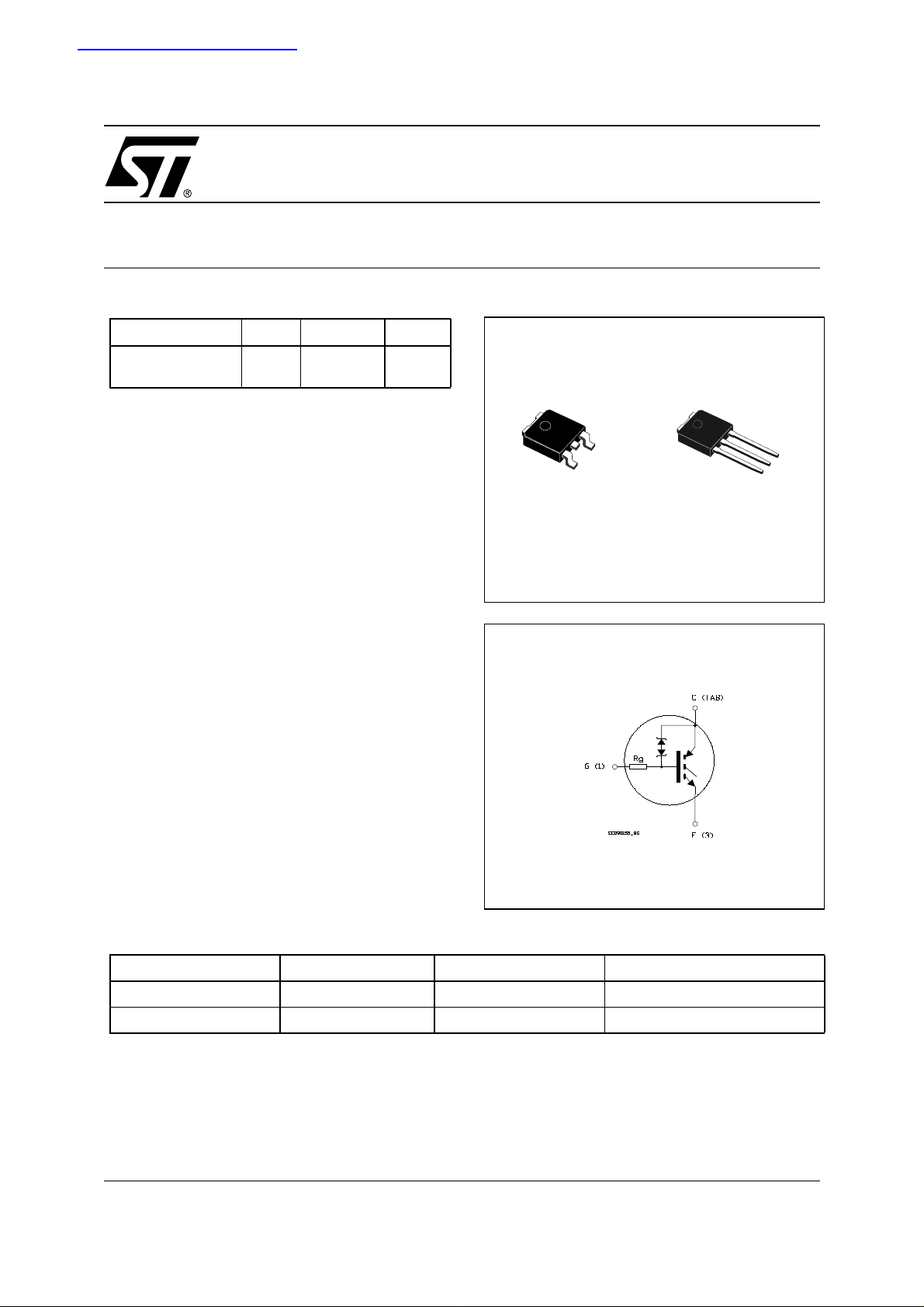
Figure 1: Package
3
1
DPAK
IPAK
Figure 2: Internal Schematic Diagram
3
2
1
Table 2: Order Code
PART NUMBER MARKING PACKAGE PACKAGING
STGD5NB120SZT4 GD5NB120SZ DPAK TAPE & REEL
STGD5NB120SZ-1 GD5NB120SZ IPAK TUBE
Rev. 2
1/13January 2005
STGD5NB120SZ-1 - STGD5NB120SZ
Table 3: Absolute Maximum ratings
Symbol Parameter Value Unit
V
CES
V
ECR
V
I
I
I
CM
P
TOT
Eas (1)
T
(
) Pulse width l i m i t ed by safe operati ng area
(1) V
CE
Table 4: Thermal Data
Rthj-case Thermal Resistance Junction-case 2.27 °C/W
Rthj-amb Thermal Resistance Junction-ambient 100 °C/W
Collector-Emitter Voltage (VGS = 0)
1200 V
Emitter-Collector Vo ltage 20 V
Gate-Emitter Voltage ±20 V
GE
Collector Current (continuous) at TC = 25°C
C
Collector Current (continuous) at TC = 100°C
C
()
Collector Current (pulsed) 20 A
Total Dissipation at TC = 25°C
10 A
5A
55 W
Derating Factor 0.44 W/°C
Single Pulse Avalanche Energy at T
Single Pulse Avalanche Energy at Tj = 100°C
Storage Temperature –55 to 150 °C
stg
T
Operating Junction Temperature range 150 °C
j
= 50 V , IAV = 3.3 A
= 25°C
j
10
7
Min. Typ. Max.
mJ
mJ
ELECTRICAL CHARACTERISTICS (T
=25°C UNLESS OTHERWISE SPECIFIED)
CASE
Table 5: On/Off
Symbol Parameter Test Conditions Min. Typ. Max. Unit
V
BR(CES)
I
CES
I
GES
V
GE(th)
V
V
CE(sat)
GE
Collector-Emitter Breakdown
Voltage
Collector cut-off Current
= 0)
(V
GE
Gate-Emitter Leakage
Current (V
CE
= 0)
Gate Threshold Voltage
Gate Emitter Voltage VCE =2.5 V, IC = 2 A,
Collector-Em itter Satur ation
Voltage
IC = 10 mA, VGE = 0 V 1200 V
= 900 V
V
CE
VCE = 900 V, Tj = 125 °C
V
= ±20V , VCE = 0 V ±100 nA
GE
V
= VGE, IC = 250 µA
CE
25V
50
250
6.5 V
Tj = 25÷125°C
VGE = 15V, IC = 5 A
V
= 15V, IC = 5 A, Tj =125°C
GE
1.3
1.2
2.0
µA
µA
V
V
2/13
STGD5NB120SZ-1 - STGD5NB120SZ
ELECTRICAL CHARACTERISTICS (CONTINUED)
Table 6: Dynamic
Symbol Parameter Test Conditions Min. Typ. Max. Unit
V
g
fs
C
ies
C
oes
C
res
Forward Transconductance
(*)
Input Capacitance
(*)
Output Capacitance 40 pF
(*) Reverse Transfer
Capacitance
R
g
(1) Pulsed: Pulse duration= 300 µs, dut y c yc l e 1.5%
Gate Resistance 4 KΩ
Table 7: Switching On
Symbol Parameter Test Conditions Min. Typ. Max. Unit
t
d(on)
t
(di/dt)
t
d(on)
t
(di/dt)
r
r
Delay Time
Current Rise Time
Turn-on Current Slope
on
Dealy Time
Current Rise Time
Turn-on Current Slope
on
Table 8: Switching Off
Symbol Paramet er Test Conditions Min. Typ. Max. Unit
Cross-over Time
Off Voltage Rise Time
)
Delay Time
)
Current Fall Time
Cross-over Time
Off Voltage Rise Time
)
Delay Time
)
Current Fall Time
tr(V
t
d(off
tr(V
td(
t
c
off
t
f
t
c
off
off
t
f
= 25 V , IC= 5 A
CE
VCE = 25V, f = 1 MHz, VGE = 0V
= 5 A , VCC = 960 V
I
C
VGE = 15 V , R
drive
=1KΩ
Tj = 25°C
= 5 A , VCC = 960 V
I
CC
VGE = 15 V , R
drive
=1KΩ
Tj = 125°C
= 5 A , VCC = 960 V
I
C
VGE = 15 V , R
drive
=1KΩ
Tj = 25°C
= 5 A , VCC = 960 V
I
C
V
= 15 V , R
GE
drive
=1KΩ
Tj = 125°C
5S
430 pF
7pF
690
170
39.6
600
185
39
4
2.2
12.1
1.13
5
2.2
12.1
2
ns
ns
A/µs
ns
ns
A/µs
µs
µs
µs
µs
µs
µs
µs
µs
Table 9: Switching Energy
Symbol Parameterr Test Conditions Min. Typ. Max Unit
Eon
(2)
Turn-on Switching Losses
E
off
E
ts
Eon (2)
E
off
E
ts
(2) Eon is the turn-on losses when a typical dio de i s used in the test circuit in figure 2.
(3) Turn-off losses in clude also the tail of the collector current.
Turn-off Switching Loss
(3)
Total Switching Loss
Turn-on Switching Losses
Turn-off Switching Loss
(3)
Total Switching Loss
= 800 V, IC = 3 A
V
CC
R
= 10 Ω, VGE= 15V, Tj= 25°C
G
(see Figure 18)
= 800 V, IC = 3 A
V
CC
R
= 10 Ω, VGE= 15V, Tj= 125°C
G
(see Figure 18)
2.59
9
11.59
2.64
10.2
12.68
mJ
mJ
mJ
mJ
mJ
mJ
3/13

STGD5NB120SZ-1 - STGD5NB120SZ
Table 10: Fu nct i onal Test
Symbol Parameterr Test Conditions Min. Typ. Max Unit
Ias Unclamped inductive switching
current
I
CL
Latching Current V
V
= 50 V, L= 1.8 mH
CC
T
= 25°C, R
start
= 960 V, Tj =125°C
CLAMP
R
=1KΩ
drive
drive
3.3 A
=1KΩ
10 A
4/13
 Loading...