


查询STGD3NB60KD 供应商
SHORT CIRCUIT PROOF PowerMESH™ IGBT
STGD3NB60KD
N-CHANNEL 3A - 600V - DPAK
TYPE V
CES
V
CE(sat)
I
C
STD3NB60KD 600 V < 2.8 V3A
■ HIGH INPUTIMPEDANCE(VOLTAGE DRIVEN)
■ LOW ON-VOLTAGE DROP (V
■ LOW ON-LOSSES
■ LOW GATE CHARGE
■ HIGH CURRENT CAPABILITY
■ OFF LOSSES INCLUDE TAIL CURRENT
■ VERY HIGH FREQUENCY OPERATION
■ SHORT CIRCUIT RATED
■ LATCH CURRENT FREE OPERA TION
■ CO-PACKAGED WITH TURBOSWITCH™
cesat
)
ANTIPARALLEL DIODE
DESCRIPTION
Using the latest h igh voltage technology based on a
patented strip layout, STMicroelectronics has
designed an advanced family of IGBTs, the
PowerMESH
™
IGBTs, with outstanding
performances. The suffix “K” identifies a fam ily
optimized for high frequency motor cont rol
applications with short circuit withstand capability.
APPLICATIONS
■ HIGH FREQUENCY MOTOR CONTROLS
■ SMPS and PFC
3
1
DPAK
INTERNAL SCHEMATIC DIAGRAM
ABSOLUTE MAXIMUM RATINGS
Symbol Parameter Value Unit
V
CES
V
ECR
V
GE
I
C
I
C
I
CM
Tsc Short Circuit Withstand 10
P
TOT
T
stg
T
j
() Pulse width limited by safe operating area
Collector-Emitter Voltage (VGS=0)
600 V
Emitter-Collector Voltage 20 V
Gate-Emitter Voltage ±20 V
Collector Current (continuous) at TC=25°C
Collector Current (continuous) at TC=100°C
()
Collector Current (pulsed) 24 A
Total Dissipation at TC= 25°C
6A
3A
35 W
Derating Factor 0.28 W/°C
Storage Temperature –65 to 150 °C
Max. Operating Junction Temperature 150 °C
µs
1/9April 2003
STGD3NB60KD
THERMAL DATA
Rthj-case Thermal Resistance Junction-case Max 3.57 °C/W
Rthj-amb Thermal Resistance Junction-ambient Max 100 °C/W
Rthc-h Thermal Resistance Case-heatsink Typ 0.5 °C/W
ELECTRICAL CHARACTERISTICS (T
= 25 °C UNLESS O THERWISE SPECIFIED)
CASE
OFF
Symbol Parameter Test Conditions Min. Typ. Max. Unit
V
BR(CES)
Collectro-Emitter Breakdown
IC= 250 µA, VGE= 0 600 V
Voltage
I
CES
I
GES
Collector cut-off
=0)
(V
GE
Gate-Emitter Leakage
Current (V
CE
=0)
V
= Max Rating, TC=25°C
CE
VCE= Max Rating, TC= 125 °C
V
=±20V,VCE= 0 ±100 nA
GE
10 µA
100 µA
ON (1)
Symbol Parameter Test Conditions Min. Typ. Max. Unit
V
GE(th)
V
CE(sat)
Gate Threshold Voltage
Collector-Emitter Saturation
Voltage
V
CE=VGE,IC
VGE=15V,IC=3A
VGE=15V,IC= 3 A, Tj =125°C
= 250µA
57V
2.4 2.8 V
1.9 V
DYNAMIC
Symbol Parameter Test Conditions Min. Typ. Max. Unit
V
g
fs
C
ies
C
oes
C
res
Q
g
Q
ge
Q
gc
Forward Transconductance
Input Capacitance
Output Capacitance
Reverse Transfer
Capacitance
Total Gate Charge
Gate-Emitter Charge
Gate-Collector Charge
tscw Short Circuit Withstand Time V
=25V,IC=3 A
CE
=25V,f=1MHz,VGE= 0 235
V
CE
1.3 2.4 S
VCE= 480V,IC=3A,
V
=15V
GE
= 0.5 BVces , VGE=15V,
ce
10 µs
Tj = 125°C , RG=10Ω
33
6.6
21
6
7.6
27
pF
pF
pF
nC
nC
nC
SWITCHING ON
Symbol Parameter Test Conditions Min. Typ. Max. Unit
t
d(on)
t
(di/dt)
r
Turn-on Delay Time
Rise Time
Turn-on Current Slope VCC= 480 V, IC=7ARG=10Ω
on
Eon Turn-on Switching Losses 37 µJ
2/9
VCC=480V,IC=3A
RG=10Ω,VGE=15V
V
= 15 V,Tj = 125°C
GE
16
30
400 A/µs
ns
ns
STGD3NB60KD
ELECTRICAL CHARACTERISTICS (CONTINUED)
SWITCHING OFF
Symbol Parameter Test Conditions Min. Typ. Max. Unit
V
t
c
tr(V
off
td(
off
t
f
E
(**)
off
E
ts
t
c
t
r(Voff
td(
off
t
f
E
(**)
off
E
ts
Note: 1. Pulsed: Pulse duration = 300 µs, duty cycle 1.5 %.
2. Pulse width limited by max. junction temperature.
(**)Losses include Also the Tail (Jedec Standardization)
Cross-over Time
)
Off Voltage Rise Time 36 ns
)
Delay Time 53 ns
Fall Time 70 ns
Turn-off Switching Loss 33
Total Switching Loss 65
Cross-over Time
)
Off Voltage Rise Time 82 ns
)
Delay Time 58 ns
Fall Time 110 ns
Turn-off Switching Loss 88
Total Switching Loss 125
= 480 V, IC=3 A,
cc
=10Ω,VGE=15V
R
GE
V
= 480 V, IC=3A,
cc
RGE=10Ω,VGE=15V
Tj = 125 °C
90 ns
180 ns
µJ
µJ
µJ
µJ
COLLECTOR-EMITTER DIODE
Symbol Parameter Test Conditions Min. Typ. Max. Unit
I
f
I
fm
V
f
t
rr
Q
rr
I
rrm
Forward Current
Forward Current pulsed
Forward On-Voltage If= 1.5 A
If= 1.5 A, Tj = 125 °C
= 1.5 A ,VR= 200 V,
Reverse Recovery Time
Reverse Recovery Charge
I
f
Tj = 125°C, di/dt = 100 A/µs
Reverse Recovery Current
1.6
1.3
90
100
2.7
1
8
2
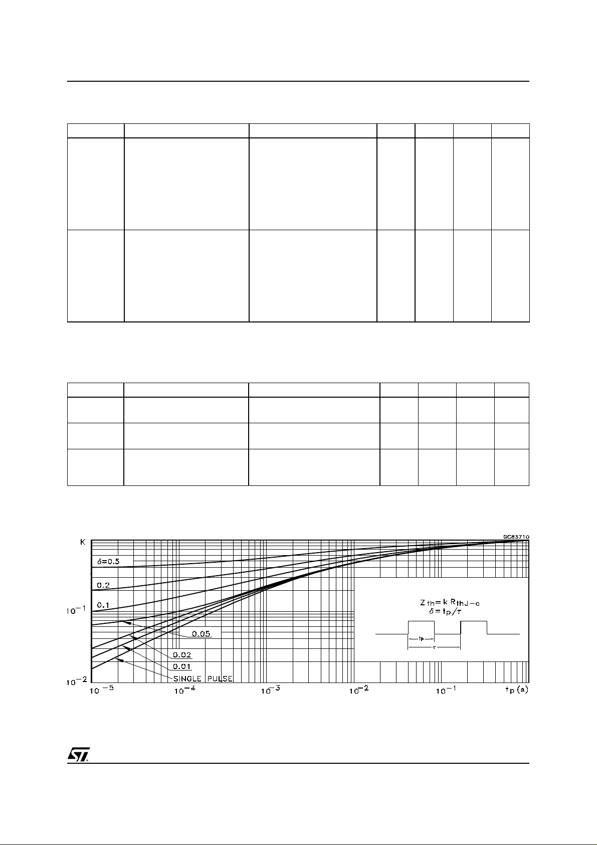
Thermal Impedance
A
A
V
V
ns
nC
A
3/9
 Loading...