

查询STGB7NB60KD供应商
STGP7NB60K-STGP7NB60KFP-STGD7NB60K
STGP7NB60KD-STGP7NB60KDFP-STGB7NB60KD
N-CHANNEL 7A - 600V - TO-220/FP/DPAK/D
2
PAK
PowerMESH™ IGBT
TYPE
STGP7NB60K
STGD7NB60K
STGP7NB60KFP
STGP7NB60KD
STGP7NB60KDFP
STGB7NB60KD
■ HIGH INPUT IMPEDANCE ( VO L TAG E DRIVEN)
■ LOW ON-VOLTAGE DROP (V
■ LOW GATE CHARGE
■ HIGH CURRENT CAPABILITY
■ OFF LOSSES INCLUDE TAIL CURRENT
■ FREQUENCY OPERATION
■ SHORT CIRCUIT RATED
V
CES
600 V
600 V
600 V
600 V
600 V
600 V
V
CE(sat)
(Typ) @125°C
< 2 V
< 2 V
< 2 V
< 2 V
< 2 V
< 2 V
)
cesat
I
C
@125°C
7 A
7 A
7 A
7 A
7 A
7 A
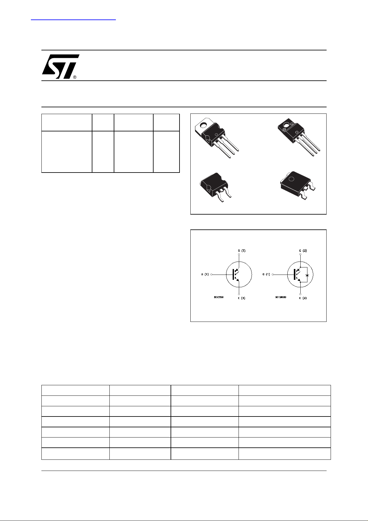
DESCRIPTION
Using the latest high voltage technology based on a
patented strip layout, STMicroelectronics has designed an advanced family of IGBTs, the Power-
™
MESH
IGBTs, with outstanding performances.
The suffix “K” identifies a family optimized for high
frequency motor control app lications with short circuit withstand capability.
3
2
TO-220
2
PAK
D
1
3
1
TO-220FP
DPAK
INTERNAL SCHEMATIC DIAGRAM
Std. Version “D” Version
3
2
1
3
1
APPLICATIONS
■ HIGH FREQUENCY MOTOR CONTROLS
■ SMPS AND PFC IN BOTH HARD SWITCHING
AND RESONANT TOPOLOG IES
ORDERING INFORMATION
SALES TYPE MARKING PACKAGE PACKAGING
STGP7NB60K GP7NB60K TO-220 TUBE
STGD7NB60KT4 GD7NB60K DPAK TAPE & REEL
STGP7NB60KFP GP7NB60KFP TO-220FP TUBE
STGP7NB60KD GP7NB60KD TO-220 TUBE
STGP7NB60KDFP GP7NB60KDFP TO-220FP TUBE
STGB7NB60KDT4
GB7NB60KD
2
PAK
D
TAPE & REEL
1/14June 2002
STGP7NB60K/STGP7NB60KFP/STGD7NB60K/STGP7NB60KD/STGB7NB60KD/STGP7NB60KDFP
ABSOLUTE MAXIMUM RATINGS
Symbol Parameter Value Unit
V
CES
V
ECR
V
I
I
I
CM
If (1)
I
fm
P
TOT
Collector-Emitter Voltage (VGS = 0)
Emitter-Collector Voltage 20 V
Gate-Emitter Voltage ±20 V
GE
Collector Current (continuous) at TC = 25°C
C
Collector Current (continuous) at TC = 125°C
C
(n)
Collector Current (pulsed) 50 50 50 A
Forward Current 7 A
(1)
Forward Current Pulsed 56 A
Total Dissipation at TC = 25°C
Derating Factor 0.64 0.28 0.64 W/°C
V
T
(n) Puls e width limited by safe operating a r ea
(1) For “D” version only
ISO
stg
T
Insulation Withstand Voltage A.C. -- 2500 -- V
Storage Temperature
Max. Operating Junction Temperature
j
TO-220
2
PAK
D
14 14 14 A
777A
95 30 90 W
TO-220FP DPAK
600 V
– 55 to 150
150
°C
THERMA L D ATA
TO-220
2
D
PAK
Rthj-case Thermal Resistance Junction-case Max 1.32 4.17 1.4 °C/W
Rthj-amb Thermal Resistance Junction-ambient Max 62.5 100 °C/W
Rthc-h Thermal Resistance Case-heatsink Typ 0.5 °C/W
TO-220FP DPAK
ELECTRICAL CHARACTERISTICS (TCASE = 25 °C UNLESS OTHERWISE SPECIFIED)
MAIN PARAMETE RS
Symbol Parameter Test Conditions Min. Typ. Max. Unit
V
BR(CES)
Collector-Emitter Breakdown
Voltage
I
CES
I
GES
Collector cut-off
(V
GE
Gate-Emitter Leakage
Current (V
V
GE(th)
V
CE(sat)
Gate Threshold Voltage
Collector-Emitter Saturation
Voltage
= 0)
CE
= 0)
IC = 250 µA, VGE = 0 600 V
V
= Max Rating, TC = 25 °C
CE
VCE = Max Rating, TC = 125 °C
V
= ±20V , VCE = 0 ±100 nA
GE
V
= VGE, IC = 250µA
CE
VGE = 15V, IC = 7 A
VGE = 15V, IC = 7 A, Tc =100°C
57V
2.3
1.9
50
500
2.8 V
µA
µA
V
2/14
STGP7NB60K/STGP7NB60KFP/STGD7NB60K/STG P7NB60KD/STGB7NB60KD/STGP7NB60KDFP
SWITCHI N G PARAMETERS
Symbol Parameter Test Conditions Min. Typ. Max. Unit
V
g
fs
C
ies
C
oes
C
res
Q
g
Q
ge
Q
gc
Forward Transconductance
Input Capacitance
Output Capacitance
Reverse Transfer
Capacitance
Total Gate Charge
Gate-Emitter Charge
Gate-Collector Charge
tscw Short Circuit Withstand Time V
t
d(on)
t
(di/dt)
Eon
t
c
tr(V
td(
off
t
E
off
E
t
c
tr(V
td(
off
t
E
off
E
r
off
f
(**)
ts
off
f
(**)
ts
Turn-on Delay Time
Rise Time
Turn-on Current Slope
on
Turn-on Switching Losses
Cross-over Time
Off Voltage Rise Time
)
Delay Time
)
Fall Time
Turn-off Switching Loss
Total Switching Loss
Cross-over Time
Off Voltage Rise Time
)
Delay Time
)
Fall Time
Turn-off Switching Loss
Total Switching Loss
= 25V, Ic = 7 A
CE
= 25V, f = 1 MHz, VGE = 0 495
V
CE
= 480V, IC = 7 A,
V
CE
VGE = 15V
= 0.5 V
ce
BR(CES)
, VGE=15V,
10 µs
Tc = 125°C , RG = 10 Ω
VCC = 480 V, IC = 7 A
RG=10Ω, VGE = 15 V
= 480 V, IC = 7 A RG=10Ω
V
CC
VGE = 15 V,Tc = 125°C
= 480 V, IC = 7 A,
V
cc
R
= 10 Ω , VGE = 15 V
GE
Tc = 25 °C
= 480 V, IC = 7 A,
V
cc
RGE = 10 Ω , VGE = 15 V
Tc = 125 °C
TBD S
77
13
32.7
45 nC
5.9
18.3
15
6
980
94
85
20
75
100
85
235
150
50
110
150
220
314
pF
pF
pF
nC
nC
ns
ns
A/µs
µJ
ns
ns
ns
ns
µJ
µJ
ns
ns
ns
ns
µJ
µJ
COLLECTOR-EMITTER DIODE (“D” VERSION)
Symbol Parameter Test Conditions Min. Typ. Max. Unit
V
Forward On-Voltage If = 3.5 A
f
If = 3.5 A, Tc = 125 °C
t
rr
Q
rr
I
rrm
Note: 1. Pulsed: Pulse dura tion = 300 µs, duty cycle 1. 5 %.
2. Pulse wi dt h l i mited by max. j unction temperature .
(**)Losses in clude Also th e T ai l (Jedec Standardization)
Reverse Recovery Time
Reverse Recovery Charge
Reverse Recovery Current
= 7 A ,VR = 35 V,
I
f
Tc=125°C, di/dt = 100A/µs
1.4
1.15
50
70
2.7
1.9
V
V
ns
nC
A
3/14
STGP7NB60K/STGP7NB60KFP/STGD7NB60K/STGP7NB60KD/STGB7NB60KD/STGP7NB60KDFP
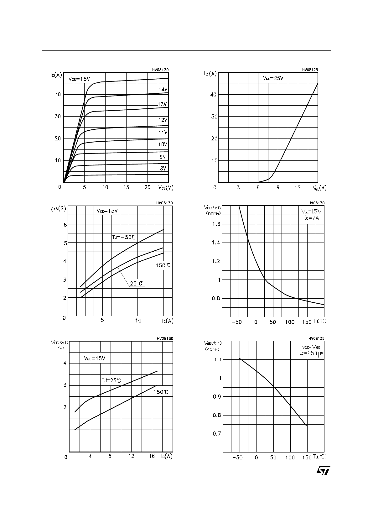
Output Characteristics
Transc onductance
Transfer Characteristics
Collector-Emitter On Voltage vs Collector Current
4/14
Gate Threshold vs Temperature
STGP7NB60K/STGP7NB60KFP/STGD7NB60K/STG P7NB60KD/STGB7NB60KD/STGP7NB60KDFP
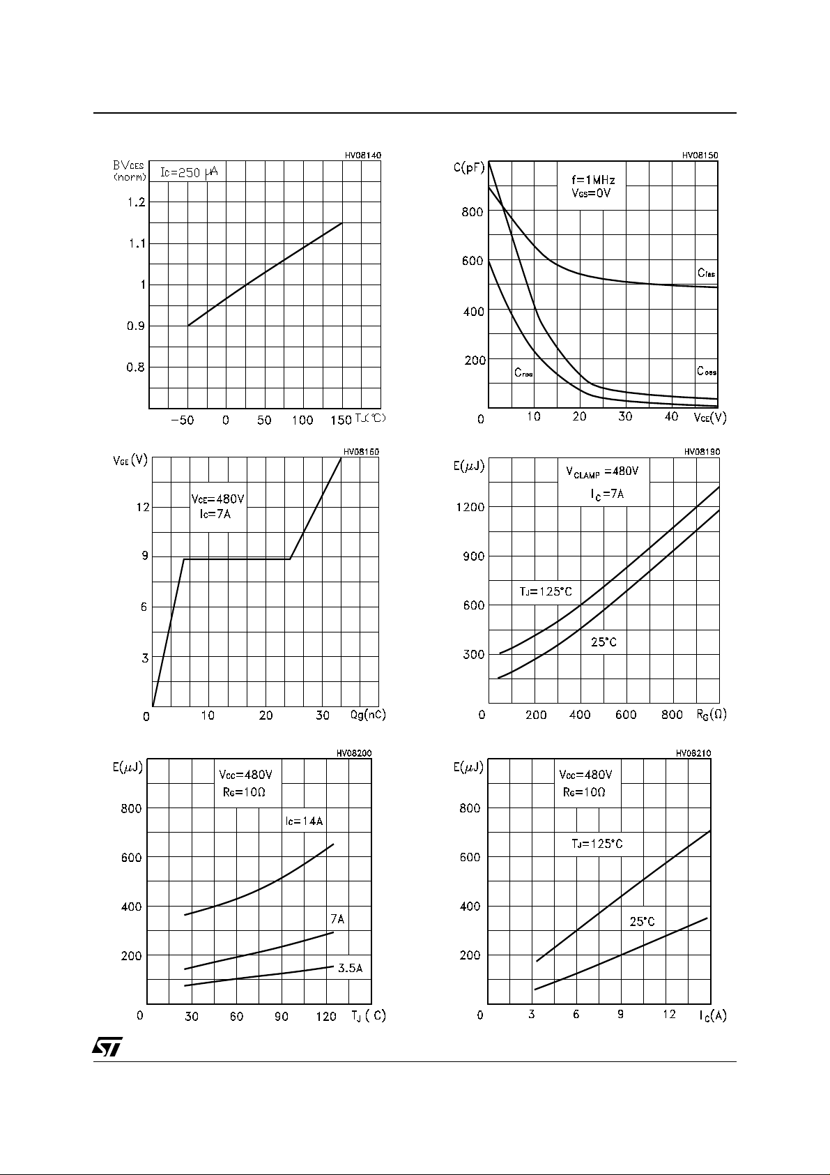
Normalized Breakdown Volta ge vs Temperature
Gate Charge vs Gate-Emitter Voltage
Capacitance Variations
Total Switching Losses vs Gate Resistance
Total Switching Losses vs Tempera ture
Total Switching Losses vs Collector Current
5/14
 Loading...