

查询STGB20NB41LZ供应商
STGB20NB41LZ
N-CHANNEL CLAMPED 20A - D²PAK
INTERNALLY CLAMPED PowerMESH™ IGBT
TYPE V
STGB20NB41LZ CLAMPED < 2.0 V20A
■ POLYSILICON GATE VOLTAGE DRIVEN
■ LOW THRE SHOLD VOLT AGE
■ LOW ON-VOLTAGE DROP
■ LOW GATE CHARGE
■ HIGH CURRENT CAPABILITY
■ HIGH VOLTAGE CLAMPING FEATURE
CES
V
CE(sat)
I
C
DESCRIPTION
Using thelatest highvoltage technology bas ed on a
patented strip layout, STMicroelectronics has
designed an advanced family of IG BTs, the
PowerMESH
™
IGBTs, with outstanding
performances. The built in collector-gate zener
exhibits a very precise active clamping while the
gate-emitter zener suppl ies an ESD protection.
APPLICATIONS
■ AUTOMOTIVE IGNITION
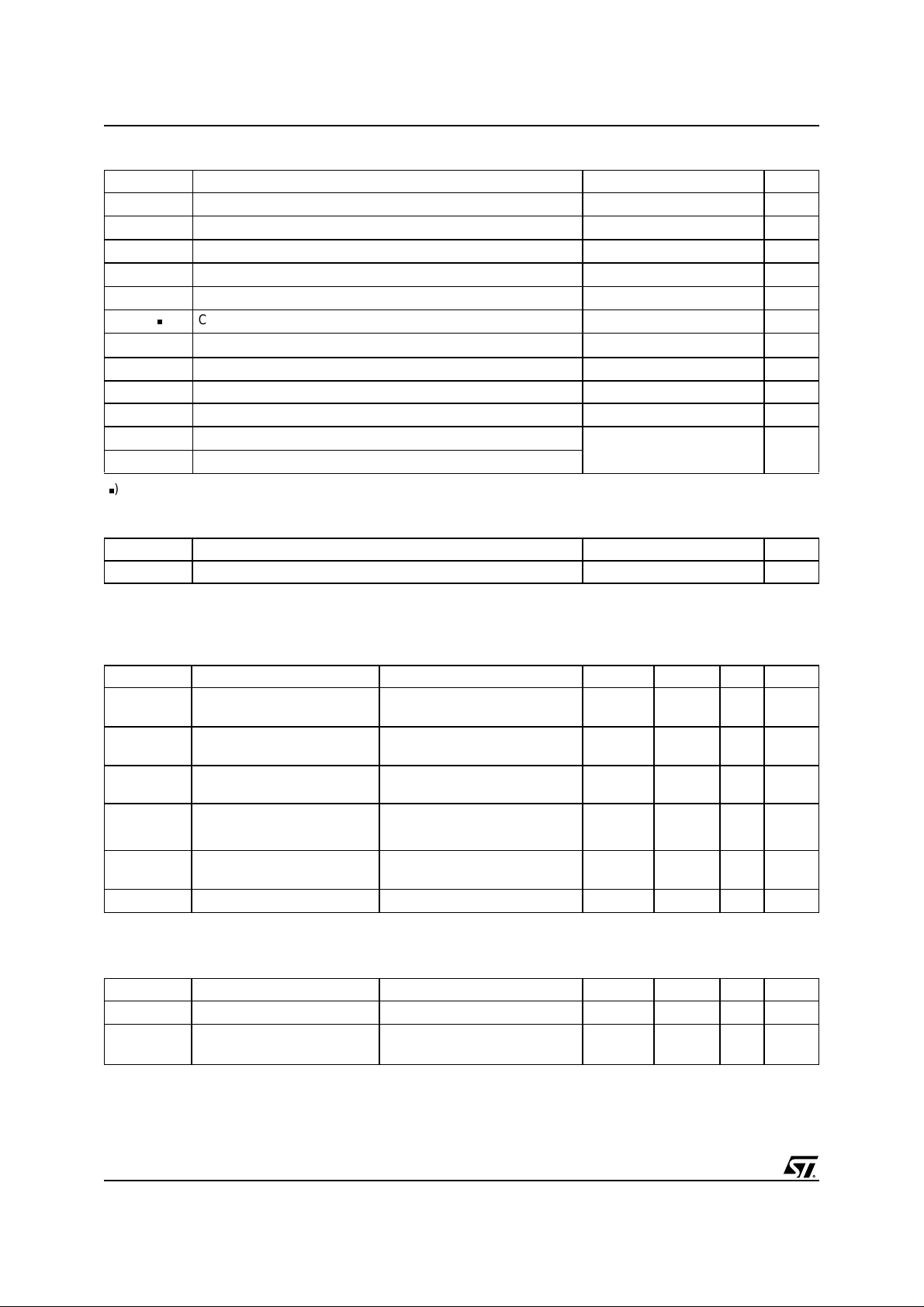
3
1
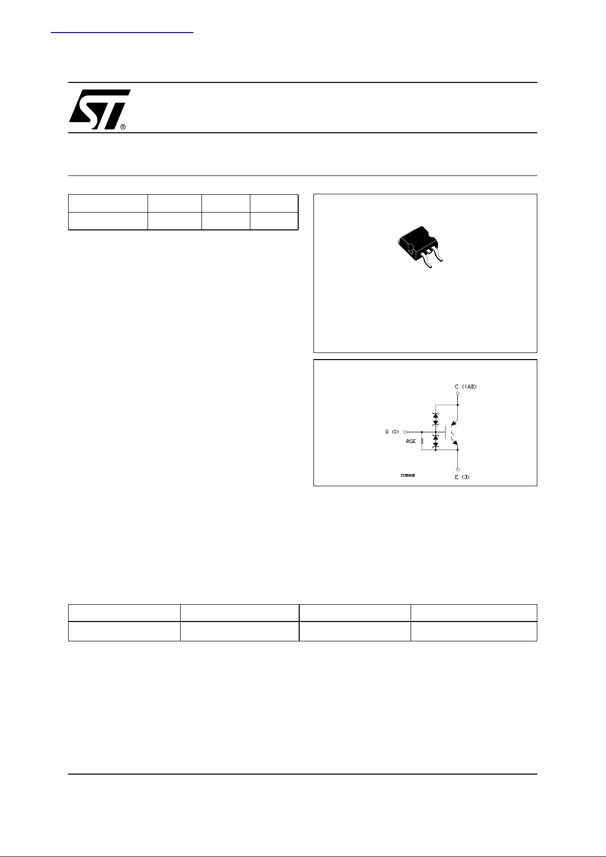
D²PAK
INTERNAL SCHEMATIC DIAGRAM
ORDER CODE
PART NUMBER MARKING PACKAGE PACKAGING
STGB20NB41LZT4 GB20NB41LZ
2
D
PAK
TAPE & REEL
1/9April 2004
STGB20NB41LZ
ABSOLUTE MAXIMUM RATINGS
Symbol Parameter Value Unit
V
CES
V
ECR
V
GE
I
C
I
C
ICM()
Eas Single Pulse Energy Tc = 25°C700
P
TOT
E
SD
T
stg
T
j
() Pulse width limited by safe operating area
THERMAL DATA
Rthj-case Thermal Resistance Junction-case Max 0.75 °C/W
Rthj-amb Thermal Resistance Junction-ambient Max 62.5 °C/W
Collector-Emitter Voltage (VGS=0)
CLAMPED V
Emitter-Collector Voltage 20 V
Gate-Emitter Voltage CLAMPED V
Collector Current (continuous) at TC=25°C
Collector Current (continuous) at TC=100°C
40 A
20 A
Collector Current (pulsed) 80 A
mJ
Total Dissipation at TC=25°C
DeratingFactor 1.33 W/°C
ESD (Human Body Model) 8 KV
Storage Temperature
Operating Junction Temperature
200 W
– 55 to 175 °C
ELECTRICAL CHARACTERISTICS (T
=25°C UNLESS OTHERWISE SPECIFIED)
CASE
OFF
Symbol Parameter Test Conditions Min. Typ. Max. Unit
BV
(CES)
Clamped Voltage IC=2mA,VGE=0,
382 412 442 V
Tc= - 40°C ÷ 150°C
BV
(ECR)
EmitterCollector Break-down
=75mA,Tc=25°C2028V
I
C
Voltage
BV
GE
Gate Emitter Break-down
IG=±2mA 12 14 16 V
Voltage
I
CES
I
GES
R
GE
Collector cut-off Current
=0)
(V
GE
Gate-Emitter Leakage
Current (V
CE
=0)
Gate Emitter Resistance 10 15 30 KΩ
=15V,VGE=0,TC=150°C
V
CE
VCE=200 V, VGE=0,TC=150°C
V
=±10V,VCE= 0 ± 300 ± 660 ±
GE
10 µA
100 µA
1000
ON (1)
Symbol Parameter Test Conditions Min. Typ. Max. Unit
V
GE(th)
V
CE(SAT)
Gate Threshold Voltage
Collector-Emitter Saturation
Voltage
V
CE=VGE,IC
= 250µA, Tc=25°C
VGE=4.5V,IC=10A,Tc=25°C
V
=4.5V,IC=20A,Tc=25°C
GE
12.4V
1.1
1.3
1.8
2.0
µA
V
V
2/9
STGB20NB41LZ
DYNAMIC
Symbol Parameter Test Conditions Min. Typ. Max. Unit
g
fs
C
ies
C
oes
C
res
Forward Transconductance
Input Capacitance VCE= 25V, f = 1 MHz, VGE= 0 2300 pF
Output Capacitance 160 pF
Reverse Transfer
Capacitance
Q
g
Gate Charge VCE= 320V,IC=20A,
FUNCTIONAL CHARACTERISTICS
Symbol Parameter Test Conditions Min. Typ. Max. Unit
II Latching Current V
U.I.S. Functional Test Open
Secondary Coil
SWITCHING ON
Symbol Parameter Test Conditions Min. Typ. Max. Unit
t
d(on)
t
r
(di/dt)
Eon Turn-on Switching Losses
Turn-on Delay Time
Rise Time
Turn-on Current Slope VCC= 320 V, IC=20A
on
=25V,IC=20 A
V
CE
V
=5V
GE
=320V,TC=125°C
Clamp
R
=1KΩ ,VGE=10V
GOFF
R
=1KΩ ,L=1.6mH,
GOFF
Tc=125°C
=320V,IC=20A
V
CC
RG=1KΩ ,VGE=5V
R
=1KΩ,VGE=5V
G
V
= 320 V, IC=20A,Tc=25°C
CC
R
=1KΩ,VGE=5V,Tc=150°C
G
35 S
25 pF
46 nC
40 A
20 A
1
0.22
140 A/µs
5mJ
5.1 mJ
µs
µs
SWITCHING OFF
Symbol Parameter Test Conditions Min. Typ. Max. Unit
V
t
c
t
r(Voff
t
d(off
t
f
E
(**)
off
t
c
tr(V
off
t
d(off
t
f
E
(**)
off
(1)Pulse width limited by max. junction temperature.
(**)Losses Include Also the Tail
Cross-over Time
)
Off Voltage Rise Time 2.5 µs
)
Delay Time 12.1 µs
FallTime 1.6 µs
Turn-off Switching Loss 12.9 mJ
Cross-over Time
)
Off Voltage Rise Time 3.16 µs
)
Delay Time 13.4 µs
FallTime 2.7 µs
Turn-off Switching Loss 18.4 mJ
= 320 V, IC=20A,
cc
R
=1KΩ ,VGE=5V
GE
= 320 V, IC=20A,
V
cc
RGE=1KΩ ,VGE=5V
Tj = 125 °C
4.4 µs
6µs
3/9
 Loading...