

STA333W
2-channel high-efficiency digital audio system
Sound Terminal™
Features
Wide supply-voltage range (4.5 V - 20 V)
2 power output configurations
– 2 channels of binary PWM (stereo mode)
– 2 channels of ternary PWM (stereo mode)
PowerSSO-36 with exposed pad down
2 channels of 24-bit DDX
100-dB SNR and dynamic range
Selectable 32- to 192-kHz input sample rates
2
I
C control with selectable device address
Digital gain -80 dB to +48 dB in 0.5-dB steps
Software volume update
Individual channel and master gain/attenuation
Individual channel and master software and
®
hardware mute
Independent channel volume bypass
Automatic zero-detect mute
Automatic invalid input detect mute
2-channel I
Selectable clock input ratio
Input channel mapping
Automatic volume control for limiting maximum
2
S input data Interface
power
96-kHz internal processing sample rate, 24-bit
precision
Advanced AM interference frequency
switching and noise suppression modes
Thermal-overload and short-circuit protection
embedded
Video application: 576 * f
input mode support
S
Table 1. Device summary
Order code Package Packaging
STA333W PowerSSO-36 EPD Tube
STA333W13TR PowerSSO-36 EPD Tape and reel
Applications
LCD
DVD
Cradle
Digital speaker
Wireless-speaker cradle
Description
The STA333W is an integrated circuit comprising
digital audio processing, digital amplifier control
and DDX
power, single-chip DDX
amplification with high quality and high efficiency.
The STA333W power section consists of four
independent half-bridges stages. These can be
configured via digital control to operate in different
modes. 2 channels can be provided by two full
bridges, providing up to 20 W + 20 W of power.
Also provided in the STA333W are new advanced
AM radio interference reduction modes. The serial
audio data input interface accepts all possible
formats, including the popular I
channels of DDX
The STA333W is part of the Sound Terminal™
family that provides full digital audio streaming to
the speaker offering cost effectiveness, low power
dissipation and sound enrichment.
®
power output stage to create a high-
®
®
processing are provided.
PowerSSO-36 package
with exposed
pad down (EPD)
solution for all-digital
2
S format. Three
January 2010 Doc ID 13365 Rev 2 1/49
www.st.com
49

Contents STA333W
Contents
1 Block diagram . . . . . . . . . . . . . . . . . . . . . . . . . . . . . . . . . . . . . . . . . . . . . . 7
2 Pin description . . . . . . . . . . . . . . . . . . . . . . . . . . . . . . . . . . . . . . . . . . . . . 8
2.1 Pin out . . . . . . . . . . . . . . . . . . . . . . . . . . . . . . . . . . . . . . . . . . . . . . . . . . . . 8
2.2 Pin list . . . . . . . . . . . . . . . . . . . . . . . . . . . . . . . . . . . . . . . . . . . . . . . . . . . . . 8
2.3 Thermal data . . . . . . . . . . . . . . . . . . . . . . . . . . . . . . . . . . . . . . . . . . . . . . 10
3 Electrical specification . . . . . . . . . . . . . . . . . . . . . . . . . . . . . . . . . . . . . . 11
3.1 Absolute maximum ratings . . . . . . . . . . . . . . . . . . . . . . . . . . . . . . . . . . . . 11
3.2 Recommended operating conditions . . . . . . . . . . . . . . . . . . . . . . . . . . . . 11
3.3 Electrical specifications - digital section . . . . . . . . . . . . . . . . . . . . . . . . . . 12
3.4 Electrical specifications - power section . . . . . . . . . . . . . . . . . . . . . . . . . . 12
3.5 Power-on/off sequences . . . . . . . . . . . . . . . . . . . . . . . . . . . . . . . . . . . . . . 14
3.6 Testing . . . . . . . . . . . . . . . . . . . . . . . . . . . . . . . . . . . . . . . . . . . . . . . . . . . 15
4 Functional description . . . . . . . . . . . . . . . . . . . . . . . . . . . . . . . . . . . . . . 16
4.1 Functional pins . . . . . . . . . . . . . . . . . . . . . . . . . . . . . . . . . . . . . . . . . . . . . 16
4.1.1 Power-down function . . . . . . . . . . . . . . . . . . . . . . . . . . . . . . . . . . . . . . . 16
4.1.2 Reset function . . . . . . . . . . . . . . . . . . . . . . . . . . . . . . . . . . . . . . . . . . . . 16
4.2 Serial audio interface description . . . . . . . . . . . . . . . . . . . . . . . . . . . . . . . 17
4.2.1 Serial audio interface protocols . . . . . . . . . . . . . . . . . . . . . . . . . . . . . . . 17
5I
2
C bus specification . . . . . . . . . . . . . . . . . . . . . . . . . . . . . . . . . . . . . . . . 18
5.1 Communication protocol . . . . . . . . . . . . . . . . . . . . . . . . . . . . . . . . . . . . . . 18
5.1.1 Data transition or change . . . . . . . . . . . . . . . . . . . . . . . . . . . . . . . . . . . . 18
5.1.2 Start condition . . . . . . . . . . . . . . . . . . . . . . . . . . . . . . . . . . . . . . . . . . . . 18
5.1.3 Stop condition . . . . . . . . . . . . . . . . . . . . . . . . . . . . . . . . . . . . . . . . . . . . 18
5.1.4 Data input . . . . . . . . . . . . . . . . . . . . . . . . . . . . . . . . . . . . . . . . . . . . . . . 18
5.2 Device addressing . . . . . . . . . . . . . . . . . . . . . . . . . . . . . . . . . . . . . . . . . . 18
5.3 Write operation . . . . . . . . . . . . . . . . . . . . . . . . . . . . . . . . . . . . . . . . . . . . . 19
5.3.1 Byte write . . . . . . . . . . . . . . . . . . . . . . . . . . . . . . . . . . . . . . . . . . . . . . . . 19
5.3.2 Multi-byte write . . . . . . . . . . . . . . . . . . . . . . . . . . . . . . . . . . . . . . . . . . . . 19
5.4 Read operation . . . . . . . . . . . . . . . . . . . . . . . . . . . . . . . . . . . . . . . . . . . . . 19
2/49 Doc ID 13365 Rev 2

STA333W Contents
5.4.1 Current address byte read . . . . . . . . . . . . . . . . . . . . . . . . . . . . . . . . . . . 19
5.4.2 Current address multi-byte read . . . . . . . . . . . . . . . . . . . . . . . . . . . . . . 19
5.4.3 Random address byte read . . . . . . . . . . . . . . . . . . . . . . . . . . . . . . . . . . 19
5.4.4 Random address multi-byte read . . . . . . . . . . . . . . . . . . . . . . . . . . . . . . 20
6 Register description . . . . . . . . . . . . . . . . . . . . . . . . . . . . . . . . . . . . . . . . 21
6.1 Configuration registers (addr 0x00 to 0x05) . . . . . . . . . . . . . . . . . . . . . . . 22
6.1.1 Configuration register A (addr 0x00) . . . . . . . . . . . . . . . . . . . . . . . . . . . 22
6.1.2 Configuration register B (addr 0x01) . . . . . . . . . . . . . . . . . . . . . . . . . . . 24
6.1.3 Configuration register C (addr 0x02) . . . . . . . . . . . . . . . . . . . . . . . . . . . 27
6.1.4 Configuration register D (addr 0x03) . . . . . . . . . . . . . . . . . . . . . . . . . . . 28
6.1.5 Configuration register E (addr 0x04) . . . . . . . . . . . . . . . . . . . . . . . . . . . 28
6.1.6 Configuration register F (addr 0x05) . . . . . . . . . . . . . . . . . . . . . . . . . . . 30
6.2 Volume control registers (addr 0x06 to 0x09) . . . . . . . . . . . . . . . . . . . . . . 32
6.2.1 Mute/line output configuration register (addr 0x06) . . . . . . . . . . . . . . . . 32
6.2.2 Master volume register (addr 0x07) . . . . . . . . . . . . . . . . . . . . . . . . . . . . 33
6.2.3 Channel volume (addr 0x08, 0x09) . . . . . . . . . . . . . . . . . . . . . . . . . . . . 33
6.3 Automodes™ register (0x0C) . . . . . . . . . . . . . . . . . . . . . . . . . . . . . . . . . . 34
6.4 Channel configuration registers (addr 0x0E, 0x0F) . . . . . . . . . . . . . . . . . 35
6.5 Variable max power correction registers (addr 0x27, 0x28) . . . . . . . . . . . 35
6.6 Variable distortion compensation registers (addr 0x29, 0x2A) . . . . . . . . . 36
6.7 Fault detect recovery constant registers (addr 0x2B, 0x2C) . . . . . . . . . . 36
6.8 Device status register (addr 0x2D) . . . . . . . . . . . . . . . . . . . . . . . . . . . . . . 36
6.9 Reserved registers (addr 0x2E, 0x2F, 0x30, 0x31) . . . . . . . . . . . . . . . . . 37
6.10 Postscale registers (addr 0x32, 0x33) . . . . . . . . . . . . . . . . . . . . . . . . . . . 37
6.11 Output limit register (addr 0x34) . . . . . . . . . . . . . . . . . . . . . . . . . . . . . . . . 38
6.11.1 Thermal and overcurrent warning output limit register . . . . . . . . . . . . . 38
7 Applications information . . . . . . . . . . . . . . . . . . . . . . . . . . . . . . . . . . . . 39
7.1 Applications scheme for power supplies . . . . . . . . . . . . . . . . . . . . . . . . . 39
7.2 PLL filter . . . . . . . . . . . . . . . . . . . . . . . . . . . . . . . . . . . . . . . . . . . . . . . . . . 39
7.3 Typical output configuration . . . . . . . . . . . . . . . . . . . . . . . . . . . . . . . . . . . 40
8 Characterization data . . . . . . . . . . . . . . . . . . . . . . . . . . . . . . . . . . . . . . . 41
9 Package thermal characteristics . . . . . . . . . . . . . . . . . . . . . . . . . . . . . . 44
Doc ID 13365 Rev 2 3/49

Contents STA333W
10 Package mechanical data . . . . . . . . . . . . . . . . . . . . . . . . . . . . . . . . . . . . 45
11 Trademarks and other acknowledgements . . . . . . . . . . . . . . . . . . . . . . 47
12 Revision history . . . . . . . . . . . . . . . . . . . . . . . . . . . . . . . . . . . . . . . . . . . 48
4/49 Doc ID 13365 Rev 2

STA333W List of tables
List of tables
Table 1. Device summary . . . . . . . . . . . . . . . . . . . . . . . . . . . . . . . . . . . . . . . . . . . . . . . . . . . . . . . . . . 1
Table 2. Pin description . . . . . . . . . . . . . . . . . . . . . . . . . . . . . . . . . . . . . . . . . . . . . . . . . . . . . . . . . . . 8
Table 3. Thermal data. . . . . . . . . . . . . . . . . . . . . . . . . . . . . . . . . . . . . . . . . . . . . . . . . . . . . . . . . . . . 10
Table 4. Absolute maximum ratings . . . . . . . . . . . . . . . . . . . . . . . . . . . . . . . . . . . . . . . . . . . . . . . . . 11
Table 5. Recommended operating conditions . . . . . . . . . . . . . . . . . . . . . . . . . . . . . . . . . . . . . . . . . 11
Table 6. Electrical characteristics for digital section . . . . . . . . . . . . . . . . . . . . . . . . . . . . . . . . . . . . . 12
Table 7. Electrical specifications for power section . . . . . . . . . . . . . . . . . . . . . . . . . . . . . . . . . . . . . 12
Table 8. Register summary. . . . . . . . . . . . . . . . . . . . . . . . . . . . . . . . . . . . . . . . . . . . . . . . . . . . . . . . 21
Table 9. Master clock select . . . . . . . . . . . . . . . . . . . . . . . . . . . . . . . . . . . . . . . . . . . . . . . . . . . . . . . 22
Table 10. MCS bits . . . . . . . . . . . . . . . . . . . . . . . . . . . . . . . . . . . . . . . . . . . . . . . . . . . . . . . . . . . . . . . 22
Table 11. Interpolation ratio select . . . . . . . . . . . . . . . . . . . . . . . . . . . . . . . . . . . . . . . . . . . . . . . . . . . 23
Table 12. IR bit settings as a function of input sample rate . . . . . . . . . . . . . . . . . . . . . . . . . . . . . . . . 23
Table 13. Thermal warning recovery . . . . . . . . . . . . . . . . . . . . . . . . . . . . . . . . . . . . . . . . . . . . . . . . . 23
Table 14. Thermal warning adjustment . . . . . . . . . . . . . . . . . . . . . . . . . . . . . . . . . . . . . . . . . . . . . . . 24
Table 15. Fault detect recovery . . . . . . . . . . . . . . . . . . . . . . . . . . . . . . . . . . . . . . . . . . . . . . . . . . . . . 24
Table 16. Serial audio input interface format . . . . . . . . . . . . . . . . . . . . . . . . . . . . . . . . . . . . . . . . . . . 25
Table 17. Serial data first bit . . . . . . . . . . . . . . . . . . . . . . . . . . . . . . . . . . . . . . . . . . . . . . . . . . . . . . . . 25
Table 18. Support serial audio input formats for MSB first (SAIFB = 0) . . . . . . . . . . . . . . . . . . . . . . . 25
Table 19. Supported serial audio input formats for LSB-First (SAIFB = 1) . . . . . . . . . . . . . . . . . . . . . 26
Table 20. Channel input mapping. . . . . . . . . . . . . . . . . . . . . . . . . . . . . . . . . . . . . . . . . . . . . . . . . . . . 27
Table 21. DDX power output mode . . . . . . . . . . . . . . . . . . . . . . . . . . . . . . . . . . . . . . . . . . . . . . . . . . 27
Table 22. DDX compensating pulse size . . . . . . . . . . . . . . . . . . . . . . . . . . . . . . . . . . . . . . . . . . . . . . 27
Table 23. Overcurrent warning detect adjustment bypass . . . . . . . . . . . . . . . . . . . . . . . . . . . . . . . . . 28
Table 24. Zero detect mute enable . . . . . . . . . . . . . . . . . . . . . . . . . . . . . . . . . . . . . . . . . . . . . . . . . . . 28
Table 25. Max power correction variable . . . . . . . . . . . . . . . . . . . . . . . . . . . . . . . . . . . . . . . . . . . . . . 28
Table 26. Max power correction . . . . . . . . . . . . . . . . . . . . . . . . . . . . . . . . . . . . . . . . . . . . . . . . . . . . . 29
Table 27. Noise-shaper bandwidth selection . . . . . . . . . . . . . . . . . . . . . . . . . . . . . . . . . . . . . . . . . . . 29
Table 28. AM mode enable. . . . . . . . . . . . . . . . . . . . . . . . . . . . . . . . . . . . . . . . . . . . . . . . . . . . . . . . . 29
Table 29. PWM speed mode . . . . . . . . . . . . . . . . . . . . . . . . . . . . . . . . . . . . . . . . . . . . . . . . . . . . . . . 29
Table 30. Distortion compensation variable enable . . . . . . . . . . . . . . . . . . . . . . . . . . . . . . . . . . . . . . 29
Table 31. Zero-crossing volume enable . . . . . . . . . . . . . . . . . . . . . . . . . . . . . . . . . . . . . . . . . . . . . . . 30
Table 32. Zero-crossing volume enable . . . . . . . . . . . . . . . . . . . . . . . . . . . . . . . . . . . . . . . . . . . . . . . 30
Table 33. Invalid input detect mute enable . . . . . . . . . . . . . . . . . . . . . . . . . . . . . . . . . . . . . . . . . . . . . 30
Table 34. Binary output mode clock loss detection . . . . . . . . . . . . . . . . . . . . . . . . . . . . . . . . . . . . . . 30
Table 35. LRCK double trigger protection . . . . . . . . . . . . . . . . . . . . . . . . . . . . . . . . . . . . . . . . . . . . . 31
Table 36. Auto EAPD on clock loss . . . . . . . . . . . . . . . . . . . . . . . . . . . . . . . . . . . . . . . . . . . . . . . . . . 31
Table 37. Power down . . . . . . . . . . . . . . . . . . . . . . . . . . . . . . . . . . . . . . . . . . . . . . . . . . . . . . . . . . . . 31
Table 38. External amplifier power down . . . . . . . . . . . . . . . . . . . . . . . . . . . . . . . . . . . . . . . . . . . . . . 31
Table 39. Master mute . . . . . . . . . . . . . . . . . . . . . . . . . . . . . . . . . . . . . . . . . . . . . . . . . . . . . . . . . . . . 32
Table 40. Channel mute . . . . . . . . . . . . . . . . . . . . . . . . . . . . . . . . . . . . . . . . . . . . . . . . . . . . . . . . . . . 32
Table 41. Master volume offset as a function of MV. . . . . . . . . . . . . . . . . . . . . . . . . . . . . . . . . . . . . . 33
Table 42. Channel volume as a function of CxV. . . . . . . . . . . . . . . . . . . . . . . . . . . . . . . . . . . . . . . . . 34
Table 43. AM interference frequency switching . . . . . . . . . . . . . . . . . . . . . . . . . . . . . . . . . . . . . . . . . 34
Table 44. Automodes™ AM switching frequency selection . . . . . . . . . . . . . . . . . . . . . . . . . . . . . . . . 34
Table 45. Status bits description. . . . . . . . . . . . . . . . . . . . . . . . . . . . . . . . . . . . . . . . . . . . . . . . . . . . . 36
Table 46. Output limit values for thermal and overcurrent warnings. . . . . . . . . . . . . . . . . . . . . . . . . . 38
Table 47. PowerSSO-36 EPD dimensions . . . . . . . . . . . . . . . . . . . . . . . . . . . . . . . . . . . . . . . . . . . . . 46
Table 48. Document revision history . . . . . . . . . . . . . . . . . . . . . . . . . . . . . . . . . . . . . . . . . . . . . . . . . 48
Doc ID 13365 Rev 2 5/49

List of figures STA333W
List of figures
Figure 1. Block diagram . . . . . . . . . . . . . . . . . . . . . . . . . . . . . . . . . . . . . . . . . . . . . . . . . . . . . . . . . . . 7
Figure 2. Pin connection (package top view) . . . . . . . . . . . . . . . . . . . . . . . . . . . . . . . . . . . . . . . . . . . 8
Figure 3. Power-on sequence . . . . . . . . . . . . . . . . . . . . . . . . . . . . . . . . . . . . . . . . . . . . . . . . . . . . . . 14
Figure 4. Power-off sequence . . . . . . . . . . . . . . . . . . . . . . . . . . . . . . . . . . . . . . . . . . . . . . . . . . . . . . 14
Figure 5. Test circuit . . . . . . . . . . . . . . . . . . . . . . . . . . . . . . . . . . . . . . . . . . . . . . . . . . . . . . . . . . . . . 15
Figure 6. Current dead-time test circuit . . . . . . . . . . . . . . . . . . . . . . . . . . . . . . . . . . . . . . . . . . . . . . . 15
Figure 7. I
Figure 8. Left justified . . . . . . . . . . . . . . . . . . . . . . . . . . . . . . . . . . . . . . . . . . . . . . . . . . . . . . . . . . . . 17
Figure 9. Write-mode sequence. . . . . . . . . . . . . . . . . . . . . . . . . . . . . . . . . . . . . . . . . . . . . . . . . . . . . 19
Figure 10. Read-mode sequence . . . . . . . . . . . . . . . . . . . . . . . . . . . . . . . . . . . . . . . . . . . . . . . . . . . . 20
Figure 11. Applications diagram . . . . . . . . . . . . . . . . . . . . . . . . . . . . . . . . . . . . . . . . . . . . . . . . . . . . . 39
Figure 12. PLL filter circuit . . . . . . . . . . . . . . . . . . . . . . . . . . . . . . . . . . . . . . . . . . . . . . . . . . . . . . . . . 40
Figure 13. Output configuration for stereo BTL mode . . . . . . . . . . . . . . . . . . . . . . . . . . . . . . . . . . . . . 40
Figure 14. Output power vs. supply voltage (THD = 1%) . . . . . . . . . . . . . . . . . . . . . . . . . . . . . . . . . . 41
Figure 15. FFT 0 dBfs (V
Figure 16. FFT -60 dBfs (V
Figure 17. THD vs. frequency (V
Figure 18. FFT 0 dBfs (V
Figure 19. FFT -60 dBfs (V
Figure 20. THD vs. frequency (V
Figure 21. Double-layer PCB with two copper ground areas and 16 vias . . . . . . . . . . . . . . . . . . . . . . 44
Figure 22. Power derating curve for PCB used as heatsink . . . . . . . . . . . . . . . . . . . . . . . . . . . . . . . . 44
Figure 23. PowerSSO-36 EPD outline drawing . . . . . . . . . . . . . . . . . . . . . . . . . . . . . . . . . . . . . . . . . 45
2
S . . . . . . . . . . . . . . . . . . . . . . . . . . . . . . . . . . . . . . . . . . . . . . . . . . . . . . . . . . . . . . . . . . . 17
= 12 V) . . . . . . . . . . . . . . . . . . . . . . . . . . . . . . . . . . . . . . . . . . . . . . . . . . 41
CC
= 12 V) . . . . . . . . . . . . . . . . . . . . . . . . . . . . . . . . . . . . . . . . . . . . . . . . 42
CC
= 18 V) . . . . . . . . . . . . . . . . . . . . . . . . . . . . . . . . . . . . . . . . . . . . . . . . . . 43
CC
CC
= 12 V, Po = 1 W) . . . . . . . . . . . . . . . . . . . . . . . . . . . . . . . . . . . . 42
CC
= 18 V) . . . . . . . . . . . . . . . . . . . . . . . . . . . . . . . . . . . . . . . . . . . . . . . . 43
= 18 V, Po = 1 W) . . . . . . . . . . . . . . . . . . . . . . . . . . . . . . . . . . . . 43
CC
6/49 Doc ID 13365 Rev 2

STA333W Block diagram
1 Block diagram
Figure 1. Block diagram
I2S
interface
Vol ume
control
PLL
DDX
I2C
Powe r
control
Protection
current/thermal
Logic
Regulators
Bias
Channel
1A
Channel
1B
Channel
2A
Channel
2B
PowerDigital DSP
Doc ID 13365 Rev 2 7/49

Pin description STA333W
2 Pin description
2.1 Pin out
Figure 2. Pin connection (package top view)
GND_SUB
SA
TEST_MODE
VSS
VCC_REG
OUT2B
GND2
VCC2
OUT2A
OUT1B
VCC1
GND1
OUT1A
GND_REG
VDD_REG
CONFIG
N.C.
N.C.
1
2
3
4
5
6
7
8
9
10
11
12
13
14
15
16
17
18
EP
exposed pad (down)
Connect to ground
36
35
34
33
32
31
30
29
28
27
26
25
24
23
22
21
20
19
D05AU1638
VDD_DIG
GND_DIG
SCL
SDA
INT_LINE
RESET
SDI
LRCKI
BICKI
XTI
GND_PLL
FILTER_PLL
VDD_PLL
PWRDN
GND_DIG
VDD_DIG
N.C.
N.C.
2.2 Pin list
Table 2. Pin description
Number Type Name Description
1 PWR GND_SUB Substrate ground
2I SA I
3 I TEST_MODE This pin must be connected to ground
4 I/O VSS Internal reference at V
5 I/O VCC_REG Internal V
6 O OUT2B Output half bridge 2B
7 PWR GND2 Power negative supply
8 PWR VCC2 Power positive supply
9 O OUT2A Output half bridge 2A
8/49 Doc ID 13365 Rev 2
2
C select address
CC
reference
- 3.3 V
CC

STA333W Pin description
Table 2. Pin description (continued)
Number Type Name Description
10 O OUT1B Output half bridge 1B
11 PWR VCC1 Power positive supply
12 PWR GND1 Power negative supply
13 O OUT1A Output half bridge 1A
14 PWR GND_REG Internal ground reference
15 PWR VDD_REG Internal 3.3-V reference voltage
16 I CONFIG Paralleled mode command
17 - N.C. No internal connection
18 - N.C. No internal connection
19 - N.C. No internal connection
20 - N.C. No internal connection
21 PWR VDD_DIG Positive supply digital
22 PWR GND_DIG Digital ground
Power down:
23 I PWRDN
0: power stage is switched off then the PLL is also
switched off (this operation take 13 million clock cycles)
1: normal operation
24 PWR VDD_PLL Positive supply for PLL
25 I FILTER_PLL Connection to PLL filter
26 PWR GND_PLL Negative supply for PLL
27 I XTI PLL input clock, 256 * f
28 I BICKI I2S serial clock
2
29 I LRCKI I
30 I SDI I
S left/right clock
2
S serial data channel
Reset:
31 I RESET
0: reset state, power stage is switched off, all registers are
set to default value
1: normal operation
32 O INT_LINE Fault interrupt
33 I/O SDA I
34 I SCL I
2
C serial data, used as SDA_OUT
2
C serial clock
35 PWR GND_DIG Digital ground
36 PWR VDD_DIG Digital supply
--EP
Exposed pad for ground-plane heatsink, to be connected
to GND
, or 384 * f
S
S
Doc ID 13365 Rev 2 9/49

Pin description STA333W
2.3 Thermal data
Table 3. Thermal data
Symbol Parameter Min Typ Max Unit
R
Th(j-case)
T
sd
T
w
T
hsd
Thermal resistance junction to case (thermal pad) - 1.5 2.0 °C/W
Thermal-shutdown junction temperature 140 150 160 °C
Thermal-warning temperature - 130 - °C
Thermal-shutdown hysteresis 18 20 22 °C
10/49 Doc ID 13365 Rev 2
STA333W Electrical specification
3 Electrical specification
3.1 Absolute maximum ratings
Table 4. Absolute maximum ratings
Symbol Parameter Min Typ Max Unit
V
CC
V
DD
I
L
T
op
T
stg
Analog supply voltage (pins VCCx) - - 23 V
Digital supply voltage (pins VDD_DIG) - - 4.0 V
Logic input interface -0.3 - 4.0 V
Operating junction temperature 0 - 150 °C
Storage temperature -40 - 150 °C
Warning: Stresses beyond those listed in Table 4: Absolute maximum
ratings may cause permanent damage to the device. These
are stress ratings only, and functional operation of the device
at these or any other conditions beyond those indicated in
Table 5: Recommended operating conditions are not implied.
Exposure to absolute-maximum-rated conditions for
extended periods may affect device reliability. In the real
application, a power supply with nominal value rated within
the limits of the recommended operating conditions, may
experience some rising beyond the maximum operating
conditions for a short time when no or very low current is
being sinked (amplifier in mute state). In this case the
reliability of the device is guaranteed, provided that the
absolute maximum ratings are not exceeded.
3.2 Recommended operating conditions
Table 5. Recommended operating conditions
Symbol Parameter Min Typ Max Unit
V
V
I
T
CC
DD
L
amb
Analog supply voltage (VCCx) 4.5 - 20.0 V
Digital supply voltage (VDD_DIG) 2.7 3.3 3.6 V
Logic input interface 2.7 3.3 3.6 V
Ambient temperature 0 - 70 °C
Doc ID 13365 Rev 2 11/49
Electrical specification STA333W
3.3 Electrical specifications - digital section
Table 6. Electrical characteristics for digital section
Symbol Parameter Conditions Min Typ Max Unit
I
il
I
ih
V
il
V
ih
V
ol
V
oh
I
pu
R
pu
Input current, no pull-up or
pull-down resistor
Low-level input voltage - - -
High-level input voltage -
Low-level output voltage Iol = 2 mA - -
High-level output voltage Ioh = 2 mA
Pull-up current - 25 66 125 µA
Equivalent pull-up
resistance
= 0 V - - ±10 µA
V
i
Vi = VDD = 3.6 V - - ±10 µA
--50-kΩ
3.4 Electrical specifications - power section
The specifications in Ta bl e 7 below are given for the conditions VCC = 18 V, VDD = 3.3 V,
f
= 384 kHz, T
SW
Table 7. Electrical specifications for power section
Symbol Parameter Conditions Min Typ Max Unit
= 25 °C and RL = 8 Ω, unless otherwise specified.
amb
0.8 *
--V
V
DD
0.8 *
--V
V
DD
0.2 *
V
DD
0.4 *
V
DD
V
V
Po Output power BTL
THD = 1% - 16 -
THD = 10% - 20 -
R
l
dss
gP
gN
I
LDT
I
HDT
t
r
t
f
dsON
Power P-channel/N-channel
MOSFET (total bridge)
Power P-channel/N-channel
leakage
Power P-channel R
dsON
matching
Power N-channel R
dsON
matching
Low-current dead time
(static)
High-current dead time
(dynamic)
Rise time
Fall time
ld = 1 A - 180 250 mΩ
V
= 18 V --10µA
CC
ld = 1 A 95--%
ld = 1 A 95--%
Resistive load,
refer to Figure 5
Refer to Figure 6 - 1020ns
Resistive load,
refer to Figure 5
Resistive load,
refer to Figure 5
12/49 Doc ID 13365 Rev 2
W
- 5 10 ns
- 8 10 ns
- 8 10 ns

STA333W Electrical specification
Table 7. Electrical specifications for power section (continued)
Symbol Parameter Conditions Min Typ Max Unit
V
CC
I
VCC
Supply voltage - 4.5 - 20 V
Supply current from VCC in
power down
PWRDN = 0 30 60 200 µA
PCM input signal = -60 dBfs
in
Supply current from V
operation
CC
Switching frequency =
384 kHz
- 3050mA
No LC filters
I
VDD_DIG
Supply current for DDX
processing (reference only)
Internal clock = 49.152 MHz 10 30 50 mA
Supply current in standby - 8 11 25 mA
I
LIM
I
SCP
V
UVP
t
min
THD+N
Overcurrent limit Non-linear output
Short-circuit protection High-impedance output
Undervoltage protection
threshold
Output minimum pulse
width
Total harmonic distortion
and noise
- - 3.5 4.3 V
No load 20 30 60 ns
DXX stereo mode, Po = 1 W,
f = 1 kHz
(1)
2.23.54.3A
(2)
2.73.85.0A
- 0.05 0.2 %
DR Dynamic range - - 100 - dB
Signal to noise ratio in
ternary mode
A-weighted - 100 -
SNR
Signal to noise ratio in
binary mode
A-weighted - 90 -
DXX stereo mode, < 5 kHz,
PSRR Power supply rejection ratio
V
RIPPLE
= 1 V RMS
-80-dB
audio input = dither only
DXX stereo mode, < 5 kHz,
X
TA L K
Crosstalk
One channel driven at 1 W
-80-dB
the other channel measured
η
1. The I
The current limit is active when OCRB = 0 (see Table 23: Overcurrent warning detect adjustment bypass
on page 28. When OCRB = 1 then I
2. The I
configuration. The short-circuit current is applicable when OCRB = 1 (see Table 23: Overcurrent warning
detect adjustment bypass on page 28.
Peak efficiency
in DXX mode
data is for 1 channel of BTL configuration, thus, 2 * I
LIM
current limit data is for 1 channel of BTL configuration, thus, 2 * I
SCP
Po = 2 x 20 W into 8 Ω -90-%
drives the 2-channel BTL configuration.
LIM
applies.
SC
drives the 2-channel BTL
SCP
dB
Doc ID 13365 Rev 2 13/49

Electrical specification STA333W
3.5 Power-on/off sequences
The power-on/off sequences shown in Figure 3 and Figure 4 below ensure a pop-free turn
on and turn off.
Figure 3. Power-on sequence
No specific VCC and VDD_DIG turn-on sequence is required
VCC
VCC
VCC
Don’t care
Don’t care
VDD_Dig
VDD_Dig
VDD_DIG
XTI
XTI
XTI
Reset
Reset
RESET
PWRDN
PWRDN
PWRDN
Bit EAPD
Soft EAPD
Soft EAPD
Register 0x05
Reg. 0x05
Reg. 0x05
Bit 7 = 1
Bit 7 = 1
Don’t care
Don’t care
Don’t care
Don’t care
TR
TR
TC
TC
TR = mimimum time between XTI master clock stable and reset removal: 1 ms
TC = minimum time between reset removal and I
Clock stable means: fmax - fmin < 1 MHz
Figure 4. Power-off sequence
No specific VCC and VDD_DIG turn-off sequence is required
VCC
VCC
VCC
VDD_DIG
VDD_Dig
VDD_Dig
XTI
XTI
XTI
Mute
Soft Mute
Soft Mute
Register 0x07
Reg. 0x07
Reg. 0x07
Data 0xFE
Data 0xFE
Bit EAPD
Soft EAPD
Soft EAPD
Register 0x05
Reg. 0x05
Reg. 0x05
Bit 7 = 0
Bit 7 = 0
Don’t care
Don’t care
2
C program sequence start: 1 ms
FE
FE
Don’t care
Don’t care
Don’t care
Don’t care
Don’t care
Don’t care
Don’t care
Don’t care
14/49 Doc ID 13365 Rev 2
STA333W Electrical specification
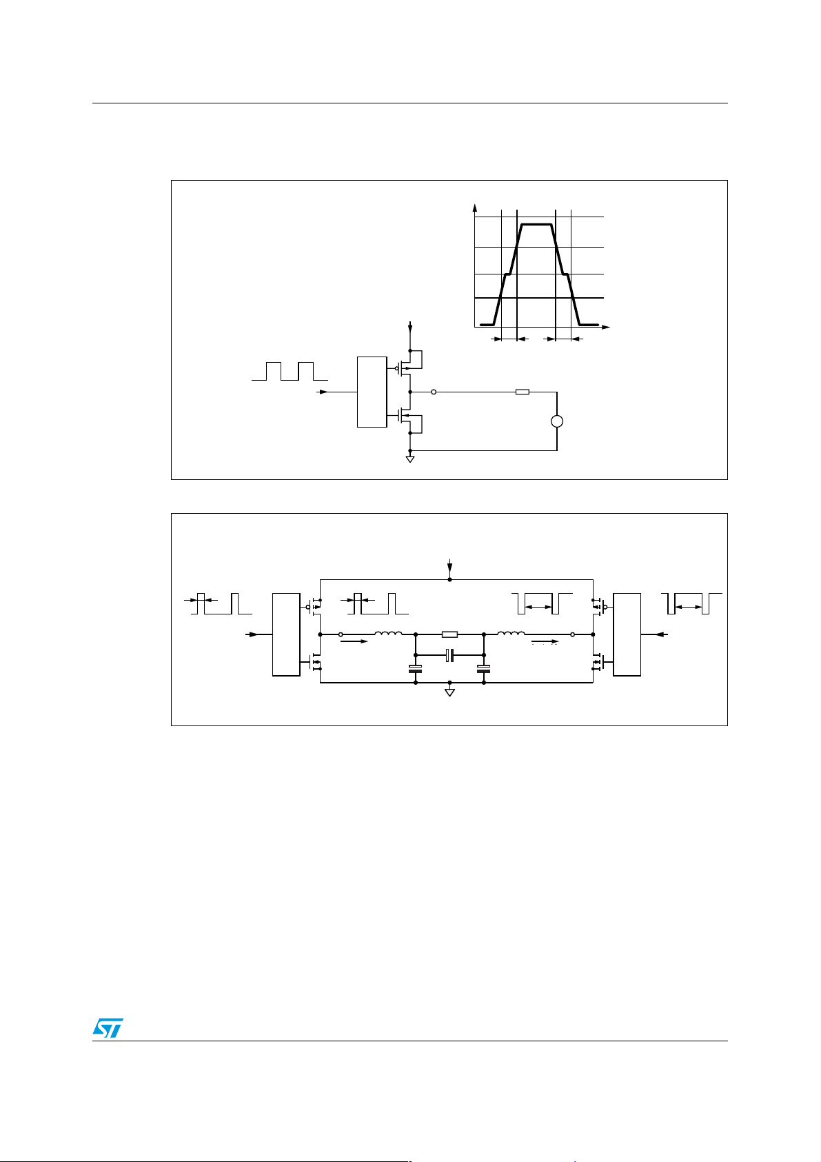
3.6 Testing
Figure 5. Test circuit
OUTxY
Vcc
(3/4)Vcc
Low current dead time = MAX(DTr,DTf)
(1/2)Vcc
(1/4)Vcc
+Vcc
t
Duty cycle = 50%
INxY
M58
M57
gnd
OUTxY
R 8Ω
DTfDTr
+
V67 =
-
vdc = Vcc/2
D03AU1458
Figure 6. Current dead-time test circuit
High Current Dead time for Bridge application = ABS(DTout(A)-DTin(A))+ABS(DTOUT(B)-DTin(B))
+V
CC
Duty cycle=A Duty cycle=B
M58
DTin(A)
INA
M57
Q1
OUTA
Iout=4A
Lout = 1.5 A
Q3
DTout(A)
C69
470nF
Rload=8Ω
C71 470nF
M64
OUTB
Q2
M63
Q4
DTout(B) DTin(B)
L68 22µL67 22µ
Iout=4A
Lout = 1.5 A
C70
470nF
INB
Duty cycle A and B: Fixed to have DC output current of 4A in the direction shown in figure
Doc ID 13365 Rev 2 15/49
D03AU1517

Functional description STA333W
4 Functional description
4.1 Functional pins
4.1.1 Power-down function
Pin PWRDN (23) is used to power down the STA333W.
PWRDN = 0 (0 V): power-down state.
PWRND = 1 (V
During the power-down sequence the output begins to mute. After the mute condition is
reached the power stage is switched off and the output becomes high impedance. Then the
master clock to all internal hardware blocks is gated off. The PLL is also switched off. The
complete power-down sequence takes 13 million cycles.
): normal operation.
DD
4.1.2 Reset function
Pin RESET (31) is used to reset the STA333W.
RESET = 0 (0 V): reset state.
RESET = 1 (V
When pin RESET is forced to 0 the power stage is switched off (with high-impedance
output) and the master clock to all internal hardware blocks is gated off.
Note: Reset has a higher priority than power down.
): normal operation.
DD
16/49 Doc ID 13365 Rev 2

STA333W Functional description
4.2 Serial audio interface description
4.2.1 Serial audio interface protocols
The STA333W serial audio input was designed to interface with standard digital audio
components and to accept serial data formats. The STA333W always acts as a slave when
receiving audio input from standard digital audio components. Serial data for two channels
is provided using 3 input pins: left/right clock LRCKI (pin 29), serial clock BICKI (pin 28), and
serial data SDI (pin 30).
The available formats are showed in Tab l e 7 and Ta bl e 8 , and set through register CONFB
on page 24.
Figure 7. I
LRCLKI
BICKI
SDI
2
S
21
3
1
2
3
Figure 8. Left justified
LRCLKI
n
n
n
n
n
-1
-1
21
3
n
-1
BICKI
SDI
1
n
1
2
3
n
-1
2
3
n
n
-1
Doc ID 13365 Rev 2 17/49

I2C bus specification STA333W
5 I2C bus specification
The STA333W supports the I2C protocol via the input ports SCL and SDA. This protocol
defines any device that sends data on to the bus as a transmitter and any device that reads
the data as a receiver. The device that controls the data transfer is known as the master and
the other as the slave. The master always starts the transfer and provides the serial clock for
synchronization. The STA333W is always a slave device in all of its communications. It
supports up to 400 kb/s (fast-mode bit rate).
5.1 Communication protocol
5.1.1 Data transition or change
Data changes on the SDA line must only occur when the SCL clock is low. SDA transition
while the clock is high is used to identify a START or STOP condition.
5.1.2 Start condition
START is identified by a high to low transition of the data bus SDA signal while the clock
signal SCL is stable in the high state. A START condition must precede any command for
data transfer.
5.1.3 Stop condition
STOP is identified by low to high transition of the data bus SDA signal while the clock signal
SCL is stable in the high state. A STOP condition terminates communication between
STA333W and the bus master.
5.1.4 Data input
During the data input the STA333W samples the SDA signal on the rising edge of clock
SCL. For correct device operation the SDA signal must be stable during the rising edge of
the clock and the data can change only when the SCL line is low.
5.2 Device addressing
To start communication between the master and the STA333W, the master must initiate a
start condition. Following this, the master sends onto the SDA line 8 bits (MSB first)
corresponding to the device-select address and read or write mode.
The 7 most significant bits are the device address identifiers, corresponding to the I
definition. In the STA333W the I
port configuration, 0x38 when SA = 0, and 0x3A when SA = 1.
The 8th bit (LSB) identifies read or write operation RW, this bit is set to 1 for read mode and
0 for write mode. After a START condition the STA333W identifies the device address on the
SDA bus and if a match is found, acknowledges the identification during the 9th bit time. The
byte following the device identification byte is the internal space address.
2
C interface has two device addresses depending on the SA
2
C bus
18/49 Doc ID 13365 Rev 2

STA333W I2C bus specification
5.3 Write operation
Following the START condition the master sends a device select code with the RW bit set
to 0. The STA333W acknowledges this and then waits for the byte of internal address. After
receiving the internal byte address the STA333W again responds with an
acknowledgement.
5.3.1 Byte write
In the byte write mode the master sends one data byte, this is acknowledged by the
STA333W. The master then terminates the transfer by generating a STOP condition.
5.3.2 Multi-byte write
The multi-byte write modes can start from any internal address. The master generating a
STOP condition terminates the transfer.
Figure 9. Write-mode sequence
BYTE
WRITE
MULTIBYTE
WRITE
DEV-ADDR
START
DEV-ADDR
START
ACK
SUB-ADD R
RW
ACK
SUB-ADD R
RW
5.4 Read operation
5.4.1 Current address byte read
Following the START condition the master sends a device select code with the RW bit set
to 1. The STA333W acknowledges this and then responds by sending one byte of data. The
master then terminates the transfer by generating a STOP condition.
5.4.2 Current address multi-byte read
The multi-byte read modes can start from any internal address. Sequential data bytes are
read from sequential addresses within the STA333W. The master acknowledges each data
byte read and then generates a STOP condition terminating the transfer.
5.4.3 Random address byte read
ACK
ACK
DATA IN
DATA IN
ACK
ACK
STOP
ACK
DATA IN
STOP
Following the START condition the master sends a device select code with the RW bit set
to 0. The STA333W acknowledges this and then the master writes the internal address byte.
After receiving, the internal byte address the STA333W again responds with an
acknowledgement. The master then initiates another START condition and sends the device
select code with the RW bit set to 1. The STA333W acknowledges this and then responds
by sending one byte of data. The master then terminates the transfer by generating a STOP
condition.
Doc ID 13365 Rev 2 19/49

I2C bus specification STA333W
5.4.4 Random address multi-byte read
The multi-byte read modes could start from any internal address. Sequential data bytes are
read from sequential addresses within the STA333W. The master acknowledges each data
byte read and then generates a STOP condition to terminate the transfer.
Figure 10. Read-mode sequence
CURRENT
ADDRESS
READ
RANDOM
ADDRESS
READ
SEQUENTIAL
CURRENT
READ
SEQUENTIAL
RANDOM
READ
START
START
START
START
DEV-ADDR
DEV-ADDR
DEV-ADDR
DEV-ADDR
RW=
HIGH
ACK
RW
ACK
SUB-ADDR
RW
ACK
ACK
SUB-ADDR
RW
DATA
DATA
NO ACK
STOP
ACK
ACK
ACK
DEV-ADDR
START RW
DATA
DEV-ADDR
START RW
ACK
ACK
ACK
DATA
DATA
DATA
NO ACK
NO ACK
ACK
STOP
STOP
DATA
ACK NO ACK
DATA
STOP
20/49 Doc ID 13365 Rev 2

STA333W Register description
6 Register description
Table 8. Register summary
Addr Name D7 D6 D5 D4 D3 D2 D1 D0
0x00 CONFA
0x01 CONFB
0x02 CONFC
0x03 CONFD
0x04 CONFE
0x05 CONFF
0x06 MUTE
0x07 MVOL
0x08 C1VOL
0x09 C2VOL
0x0C AUTO
0x0E C1CFG
0x0F C2CFG
0x27 MPCC1
0x28 MPCC2
0x29 DCC1
0x2A DCC2
0x2B FDRC1
0x2C FDRC2
0x2D STATUS
0x2E BIST1
0x2F BIST2
0x30 BIST3
0x31 TSTCTL
0x32 C1PS
0x33 C2PS
0x34 OLIM
FDRB TWAB TWRB IR1 IR0 MCS2 MCS1 MCS0
C2IM C1IM Reserved SAIFB SAI3 SAI2 SAI1 SAI0
OCRB Reserved CSZ3 CSZ2 CSZ1 CSZ0 OM1 OM0
Reserved ZDE Reserved
SVE ZCE DCCV PWMS AME NSBW MPC MPCV
EAPD PWDN ECLE LDTE BCLE IDE Reserved
Reserved C2M C1M MMUTE
MV7 MV6 MV5 MV4 MV3 MV2 MV1 MV0
C1V7 C1V6 C1V5 C1V4 C1V3 C1V2 C1V1 C1V0
C2V7 C2V6 C2V5 C2V4 C2V3 C2V2 C2V1 C2V0
Reserved AMAM2 AMAM1 AMAM0 AMAME
Reserved C1VBP Reserved
Reserved C2VBP Reserved
MPCC15 MPCC14 MPCC13 MPCC12 MPCC11 MPCC10 MPCC9 MPCC8
MPCC7 MPCC6 MPCC5 MPCC4 MPCC3 MPCC2 MPCC1 MPCC0
DCC15 DCC14 DCC13 DCC12 DCC11 DCC10 DCC9 DCC8
DCC7 DCC6 DCC5 DCC4 DCC3 DCC2 DCC1 DCC0
FDRC15 FDRC14 FDRC13 FDRC12 FDRC11 FDRC10 FDRC9 FDRC8
FDRC7 FDRC6 FDRC5 FDRC4 FDRC3 FDRC2 FDRC1 FDRC0
PLLUL FAULT UVFAULT Reserved OCFAULT OCWARN TFAULT TWARN
Reserved RO1BACT R5BACT R4BACT R3BACT R2BACT R1BACT
Reserved R01BEND R5BEND R4BEND R3BEND R2BEND R1BEND
Reserved R5BBAD R4BBAD R3BBAD R1BBAD R1BBAD
Reserved
C1PS7 C1PS6 C1PS5 C1PS4 C1PS3 C1PS2 C1PS1 C1PS0
C2PS7 C2PS6 C2PS5 C2PS4 C2PS3 C2PS2 C2PS1 C2PS0
OLIM7 OLIM6 OLIM5 OLIM4 OLIM3 OLIM2 OLIM1 OLIM0
Doc ID 13365 Rev 2 21/49

Register description STA333W
6.1 Configuration registers (addr 0x00 to 0x05)
6.1.1 Configuration register A (addr 0x00)
D7 D6 D5 D4 D3 D2 D1 D0
FDRB TWAB TWRB IR1 IR0 MCS2 MCS1 MCS0
01100011
Master clock select
Table 9. Master clock select
Bit R/W RST Name Description
0R/W1MCS0
1R/W1MCS1
2R/W0MCS2
The STA333W supports sample rates of 32 kHz, 44.1 kHz, 48 KHz, 88.2 kHz, 96 kHz,
176.4 kHz, and 192 kHz. Therefore the internal clock is:
z 32.768 MHz for 32 kHz
z 45.1584 MHz for 44.1 kHz, 88.2 kHz, and 176.4 kHz
z 49.152 MHz for 48 kHz, 96 kHz, and 192 kHz
Master clock select: Selects the ratio between the
2
input I
S sample frequency and the input clock.
The external clock frequency provided to the XTI pin must be a multiple of the input sample
frequency (f
).
S
The relationship between the input clock and the input sample rate is determined by both
the MCSx and the IR (input rate) register bits. The MCSx bits determine the PLL factor
generating the internal clock and the IR bit determines the oversampling ratio used
internally.
Table 10. MCS bits
Input sample rate
fS (kHz)
32, 44.1, 48 00 576 * f
IR
101 100 011 010 001 000
128 * f
S
88.2, 96 01 NA 64 * f
176.4, 192 1X NA 32 * f
S
S
S
MCS[2:0]
256 * fS384 * fS512 * fS768 * f
128 * fS192 * fS256 * fS384 * f
64 * f
96 * fS128 * fS192 * f
S
S
S
S
22/49 Doc ID 13365 Rev 2

STA333W Register description
Interpolation ratio select
Table 11. Interpolation ratio select
Bit R/W RST Name Description
4:3 R/W 00 IR [1:0]
Interpolation ratio select: Selects internal
interpolation ratio based on input I
2
S sample
frequency.
The STA333W has variable interpolation (oversampling) settings such that internal
processing and DDX output rates remain consistent. The first processing block interpolates
by either 2 times or 1 time (pass-through) or provides a 2-times downsample. The
oversampling ratio of this interpolation is determined by the IR bits.
Table 12. IR bit settings as a function of input sample rate
Input sample rate fS (kHz) IR 1st stage interpolation ratio
32 00 2-times oversampling
44.1 00 2-times oversampling
48 00 2-times oversampling
88.2 01 Pass-through
96 01 Pass-through
176.2 10 2-times downsampling
192 10 2-times downsampling
Thermal warning recovery bypass
Table 13. Thermal warning recovery
Bit R/W RST Name Description
Thermal warning recovery bypass:
5R/W1TWRB
0: thermal warning recovery enabled
1: thermal warning recovery disabled
If the thermal warning adjustment is enabled (TWAB = 0), then the thermal warning
recovery determines if the -3 dB output limit is removed when thermal warning is negative.
If TWRB = 0 and TWAB = 0, then when a thermal warning disappears the -3 dB output limit
is removed and the gain is added back to the system. If TWRB = 1 and TWAB = 0, then
when a thermal warning disappears the -3 dB output limit remains until TWRB is changed to
zero or the device is reset.
Doc ID 13365 Rev 2 23/49

Register description STA333W
Thermal warning adjustment bypass
Table 14. Thermal warning adjustment
Bit R/W RST Name Description
Thermal warning adjustment bypass:
6R/W1TWAB
0: thermal warning adjustment enabled
1: thermal warning adjustment disabled
The on-chip STA333W power output block provides feedback to the digital controller using
inputs to the power control block. The TWARN input is used to indicate a thermal warning
condition. When TWARN is asserted (set to 0) for a period of time greater than 400 ms, the
power control block will force a -3dB output limit (determined by TWOCL in coefficient RAM)
to the modulation limit in an attempt to eliminate the thermal warning condition. Once the
thermal warning output limit adjustment is applied, it remains in this state until reset, unless
FDRB = 0.
Fault detect recovery bypass
Table 15. Fault detect recovery
Bit R/W RST Name Description
7R/W0FDRB
The on-chip STA333W power output block provides feedback to the digital controller using
inputs to the power control block. The FAULT input is used to indicate a fault condition (either
overcurrent or thermal). When FAULT is asserted (set to 0), the power control block attempts
a recovery from the fault by asserting the 3-state output (setting it to 0 which directs the
power output block to begin recovery), holding it at 0 for period of time in the range of 0.1 ms
to 1 second as defined by the fault detect recovery constant register (FDRC registers 0x2B,
0x2C), then toggling it back to 1. This sequence is repeated as log as the fault indication
exists. This feature is enabled by default but can be bypassed by setting the FDRB control
bit to 1.
6.1.2 Configuration register B (addr 0x01)
D7 D6 D5 D4 D3 D2 D1 D0
C2IM C1IM Reserved SAIFB SAI3 SAI2 SAI1 SAI0
10000000
Fault detect recovery bypass:
0: fault detect recovery enabled
1: fault detect recovery disabled
24/49 Doc ID 13365 Rev 2

STA333W Register description
Serial audio input interface format
Table 16. Serial audio input interface format
Bit R/W RST Name Description
0R/W0SAI0
1R/W0SAI1
2R/W0SAI2
Determines the interface format of the input serial
digital audio interface.
3R/W0SAI3
Serial data interface
The STA333W audio serial input interfaces with standard digital audio components and
accepts a number of serial data formats. STA333W always acts a slave when receiving
audio input from standard digital audio components. Serial data for two channels is provided
using three inputs: left/right clock LRCKI, serial clock BICKI, and serial data SDI.
Bits SAI and bit SAIFB are used to specify the serial data format. The default serial data
format is I
2
S, MSB first. Available formats are shown in the tables and figure that follow.
Serial data first bit
Table 17. Serial data first bit
SAIFB Format
0 MSB-first
1 LSB-first
Table 18. Support serial audio input formats for MSB first (SAIFB = 0)
BICKI SAI [3:0] SAIFB Interface format
32 * f
48* f
S
S
0000 0 I2S 15-bit data
0001 0 Left/right justified 16-bit data
0000 0 I2S 16- to 23-bit data
0001 0 Left justified 16- to 24-bit data
0010 0 Right justified 24-bit data
0110 0 Right justified 20-bit data
1010 0 Right justified 18-bit data
1110 0 Right justified 16-bit data
Doc ID 13365 Rev 2 25/49

Register description STA333W
Table 18. Support serial audio input formats for MSB first (SAIFB = 0) (continued)
0000 0 I2S 16- to 24-bit data
0001 0 Left justified 16- to 24-bit data
64* f
S
Table 19. Supported serial audio input formats for LSB-First (SAIFB = 1)
BICKI SAI[3:0] SAIFB Interface format
0010 0 Right justified 24-bit data
0110 0 Right justified 20-bit data
1010 0 Right justified 18-bit data
1110 0 Right justified 16-bit data
32* f
48* f
48* f
1100 1 I2S 15-bit data
S
1110 1 Left/right justified 16-bit data
0100 1 I2S 23-bit data
0100 1 I
1000 1 I
1100 1 LSB first I
S
0001 1 Left justified 24-bit data
2
S 20-bit data
2
S 18-bit data
2
S 16-bit data
0101 1 Left justified 20-bit data
1001 1 Left justified 18-bit data
1101 1 Left justified 16-bit data
0010 1 Right justified 24-bit data
0110 1 Right justified 20-bit data
S
1010 1 Right justified 18-bit data
1110 1 Right justified 16-bit data
0000 1 I2S 24-bit data
0100 1 I
1000 1 I
1100 1 LSB First I
2
S 20-bit data
2
S 18-bit data
2
S 16-bit data
0001 1 Left justified 24-bit data
0101 1 Left justified 20-bit data
64* f
S
1001 1 Left justified 18-bit data
1101 1 Left justified 16-bit data
0010 1 Right justified 24-bit data
0110 1 Right justified 20-bit data
1010 1 Right justified 18-bit data
1110 1 Right justified 16-bit data
26/49 Doc ID 13365 Rev 2

STA333W Register description
Channel input mapping
Table 20. Channel input mapping
Bit R/W RST Name Description
2
6R/W0C1IM
7R/W0C2IM
0: processing channel 1 receives left I
1: processing channel 1 receives right I2S input
0: processing channel 2 receives left I
1: processing channel 2 receives right I2S input
S input
2
S input
Each channel received via I2S can be mapped to any internal processing channel via the
channel input mapping registers. This allows for flexibility in processing. The default settings
of these registers map each I
2
S input channel to its corresponding processing channel.
6.1.3 Configuration register C (addr 0x02)
D7 D6 D5 D4 D3 D2 D1 D0
OCRB Reserved CSZ3 CSZ2 CSZ1 CSZ0 OM1 OM0
10010111
DDX power output mode
Table 21. DDX power output mode
Bit R/W RST Name Description
0 R/W 1 OM0 The DDX power output mode selects the configuration
of the DDX output:
00: drop compensation
1R/W1OM1
01: discrete output stage: tapered compensation
10: full-power mode
11: variable drop compensation (CSZx bits)
DDX compensation pulse size register
Table 22. DDX compensating pulse size
Bit R/W RST Name Description
2 R/W 1 CSZ0 When OM[1:0] = 11, this register determines the size of
3R/W0CSZ1
4R/W1CSZ2
5R/W0CSZ3
the DDX compensating pulse from 0 to 15 clock periods:
0000: 0 ns (0 ticks) compensating pulse size
0001: 20 ns (1 tick) clock period compensating pulse
size
.....
1111: 300 ns (15 ticks) clock period compensating pulse
size
Doc ID 13365 Rev 2 27/49

Register description STA333W
Overcurrent warning detect adjustment bypass
Table 23. Overcurrent warning detect adjustment bypass
Bit R/W RST Name Description
7R/W1OCRB
0: overcurrent warning adjustment enabled
1: overcurrent warning adjustment disabled
The status bit OCWARN is used to warn of an overcurrent condition. When OCWARN is
asserted (set to 0), the power control block forces an adjustment to the modulation limit
(default -3dB) in an attempt to eliminate the overcurrent warning condition. Once the
overcurrent warning volume adjustment is applied, it remains applied until the device is
reset. The overcurrent limit can be changed via register OLIM (Output limit register (addr
0x34) on page 38).
6.1.4 Configuration register D (addr 0x03)
D7 D6 D5 D4 D3 D2 D1 D0
Reserved ZDE Reserved
01000000
Zero-detect mute enable
Table 24. Zero detect mute enable
Bit R/W RST Name Description
6 R/W 1 ZDE 1: enable the automatic zero-detect mute
Setting the ZDE bit enables the zero-detect automatic mute. The zero-detect circuit looks at
the data for each processing channel at the output of the crossover (bass management)
filter. If any channel receives 2048 consecutive zero value samples (regardless of f
) then
S
that individual channel is muted if this function is enabled.
6.1.5 Configuration register E (addr 0x04)
D7 D6 D5 D4 D3 D2 D1 D0
SVE ZCE DCCV PWMS AME NSBW MPC MPCV
11000010
Max power correction variable
Table 25. Max power correction variable
Bit R/W RST Name Description
0R/W0MPCV
0: use standard MPC coefficient
1: use MPCC bits for MPC coefficient
28/49 Doc ID 13365 Rev 2

STA333W Register description
Max power correction
Table 26. Max power correction
Bit R/W RST Name Description
1R/W1MPC
1: enable power bridge correction for THD reduction
near maximum power output.
Setting the MPC bit turns on special processing that corrects the STA333W power device at
high power. This mode lowers the THD+N of a full DDX system at maximum power output
and slightly below. If enabled, MPC is operational in all output modes except tapered
(OM[1:0] = 01) and binary. When OCFG = 00, MPC does not affect channels 3 and 4, the
line-out channels.
Noise-shaper bandwidth selection
Table 27. Noise-shaper bandwidth selection
Bit R/W RST Name Description
rd
1: 3
2R/W0NSBW
order NS
0: 4th order NS
AM mode enable
Table 28. AM mode enable
Bit R/W RST Name Description
3R/W0AME
0: normal DDX operation
1: AM reduction mode DDX operation
The STA333W features a DDX processing mode that minimizes the amount of noise
generated in frequency range of AM radio. This mode is intended for use when DDX is
operating in a device with an AM tuner active. The SNR of the DDX processing is reduced to
approximately 83 dB in this mode, which is still greater than the SNR of AM radio.
PWM speed mode
Table 29. PWM speed mode
Bit R/W RST Name Description
4R/W0PWMS
0: normal speed (384 kHz) all channels
1: odd speed (341.3 kHz) all channels
Distortion compensation variable enable
Table 30. Distortion compensation variable enable
Bit R/W RST Name Description
5 R/W 0 DCCV
Doc ID 13365 Rev 2 29/49
0: uses preset DC coefficient.
1: uses DCC coefficient.

Register description STA333W
Zero-crossing volume enable
Table 31. Zero-crossing volume enable
Bit R/W RST Name Description
1: volume adjustments will only occur at digital
6R/W1ZCE
zero-crossings
0: volume adjustments will occur immediately
The ZCE bit enables zero-crossing volume adjustments. When volume is adjusted on digital
zero-crossings no clicks will be audible.
Soft volume update enable
Table 32. Zero-crossing volume enable
Bit R/W RST Name Description
1: volume adjustments ramp according to SVR
7R/W1SVE
settings
0: volume adjustments will occur immediately
6.1.6 Configuration register F (addr 0x05)
D7 D6 D5 D4 D3 D2 D1 D0
EAPD PWDN ECLE LDTE BCLE IDE Reserved
0101110 0
Invalid Input detect mute enable
Table 33. Invalid input detect mute enable
Bit R/W RST Name Description
2 R/W 1 IDE 1: enables the automatic invalid input detect mute
Setting the IDE bit enables this function, which looks at the input I2S data and will
automatically mute if the signals are perceived as invalid.
Binary output mode clock loss detection
Table 34. Binary output mode clock loss detection
Bit R/W RST Name Description
3 R/W 1 BCLE Binary output mode clock loss detection enable
Detects loss of input MCLK in binary mode and outputs 50% of the duty cycle.
30/49 Doc ID 13365 Rev 2

STA333W Register description
LRCK double trigger protection
Table 35. LRCK double trigger protection
Bit R/W RST Name Description
4 R/W 1 LDTE LRCLK double trigger protection enable
Actively prevents double trigger of LRCLK.
Auto EAPD on clock loss
Table 36. Auto EAPD on clock loss
Bit R/W RST Name Description
5 R/W 0 ECLE Auto EAPD on clock loss
When active will issue a power device power-down signal (EAPD) on clock loss detection.
IC power down
Table 37. Power down
Bit R/W RST Name Description
6R/W1PWDN
0: power down, low-power condition
1: normal operation
The PWDN register is used to put the IC in a low-power state. When PWDN is 0, the output
begins a soft-mute. After the mute condition is reached, EAPD is asserted to power down
the power stage, then the master clock to all internal hardware except the I
2
C block is gated.
This puts the IC in a very low power consumption state.
External amplifier power down
Table 38. External amplifier power down
Bit R/W RST Name Description
7 R/W 1 EAPD
The EAPD register directly disables/enables the internal power circuitry.
When EAPD = 0, the internal power section is placed in a low-power state (disabled).
0: external power stage power down active
1: normal operation
Doc ID 13365 Rev 2 31/49

Register description STA333W
6.2 Volume control registers (addr 0x06 to 0x09)
6.2.1 Mute/line output configuration register (addr 0x06)
D7 D6 D5 D4 D3 D2 D1 D0
Reserved C2M C1M MMUTE
00000000
Master mute
Table 39. Master mute
Bit R/W RST Name Description
0R/W0MMUTE
0: normal operation
1: all channels are in mute condition
Channel mute
Table 40. Channel mute
Bit R/W RST Name Description
Channel 1 mute:
1R/W0C1M
2R/W0C2M
0: not muted, it is possible to set the channel volume
1: hardware muted
Channel 2 mute:
0: not muted, it is possible to set the channel volume
1: hardware muted
32/49 Doc ID 13365 Rev 2

STA333W Register description
6.2.2 Master volume register (addr 0x07)
D7 D6 D5 D4 D3 D2 D1 D0
MV7 MV6 MV5 MV4 MV3 MV2 MV1 MV0
11111111
6.2.3 Channel volume (addr 0x08, 0x09)
D7 D6 D5 D4 D3 D2 D1 D0
C1V7 C1V6 C1V5 C1V4 C1V3 C1V2 C1V1 C1V0
01100000
D7 D6 D5 D4 D3 D2 D1 D0
C2V7 C2V6 C2V5 C2V4 C2V3 C2V2 C2V1 C2V0
01100000
Volume setting
The volume structure of the STA333W consists of individual volume registers for each
channel and a master volume register that provides an offset to each channels volume
setting. The individual channel volumes are adjustable in 0.5-dB steps from +48 dB to
-80 dB. As an example if C3V = 0x00 or +48 dB and MV = 0x18 or -12 dB, then the total gain
for channel 3 = +36 dB.
The master mute when set to 1 will mute all channels at once, whereas the individual
channel mutes (CxM) mute only that channel. Both the master mute and the channel mutes
provide a “soft mute” with the volume ramping down to mute in 4096 samples from the
maximum volume setting at the internal processing rate (about 96 kHz). A hard mute can be
obtained by commanding a value of all 1’s (255) to any channel volume register or the
master volume register. When volume offsets are provided via the master volume register
any channel that whose total volume is less than -80 dB is muted.
All changes in volume take place at zero-crossings when ZCE = 1 (configuration register F)
on a per channel basis as this creates the smoothest possible volume transitions. When
ZCE = 0, volume updates will occur immediately.
Table 41. Master volume offset as a function of MV
MV[7:0] Volume offset from channel value
00000000 (0x00) 0 dB
00000001 (0x01) -0.5 dB
00000010 (0x02) -1 dB
……
01001100 (0x4C) -38 dB
……
11111110 (0xFE) -127.5 dB
11111111 (0xFF) Hard master mute
Doc ID 13365 Rev 2 33/49

Register description STA333W
Table 42. Channel volume as a function of CxV
CxV[7:0] Volume
00000000 (0x00) +48 dB
00000001 (0x01) +47.5 dB
00000010 (0x02) +47 dB
……
01011111 (0x5F) +0.5 dB
01100000 (0x60) 0 dB
01100001 (0x61) -0.5 dB
……
11010111 (0xD7) -59.5 dB
11011000 (0xD8) -60 dB
11011001 (0xD9) -61 dB
11011010 (0xDA) -62 dB
……
11101100 (0xEC) -80 dB
11101101 (0xED) Hard channel mute
……
11111111 (0xFF) Hard channel mute
6.3 Automodes™ register (0x0C)
D7 D6 D5 D4 D3 D2 D1 D0
Reserved AMAM2 AMAM1 AMAM0 AMAME
00000000
AM interference frequency switching
Table 43. AM interference frequency switching
Bit R/W RST Name Description
0R/W0AMAME
AMAM bits
Table 44. Automodes™ AM switching frequency selection
AMAM[2:0] 48 kHz / 96 kHz input f
000 0.535 MHz - 0.720 MHz 0.535 MHz - 0.670 MHz
0: switching frequency determined by PWMS setting
1: switching frequency determined by AMAM setting
S
44.1 kHz / 88.2 kHz input f
S
001 0.721 MHz - 0.900 MHz 0.671 MHz - 0.800 MHz
34/49 Doc ID 13365 Rev 2

STA333W Register description
Table 44. Automodes™ AM switching frequency selection
010 0.901 MHz - 1.100 MHz 0.801 MHz - 1.000 MHz
011 1.101 MHz - 1.300 MHz 1.001 MHz - 1.180 MHz
100 1.301 MHz - 1.480 MHz 1.181 MHz - 1.340 MHz
101 1.481 MHz - 1.600 MHz 1.341 MHz - 1.500 MHz
110 1.601 MHz - 1.700 MHz 1.501 MHz - 1.700 MHz
6.4 Channel configuration registers (addr 0x0E, 0x0F)
D7 D6 D5 D4 D3 D2 D1 D0
Reserved C1VBP Reserved
00000000
D7 D6 D5 D4 D3 D2 D1 D0
Reserved C2VBP Reserved
00000000
Volume bypass
Each channel contains an individual channel volume bypass. If a particular channel has
volume bypassed via the CxVBP = 1 register then only the channel volume setting for that
particular channel affects the volume setting, the master volume setting will not affect that
channel.
6.5 Variable max power correction registers (addr 0x27, 0x28)
MPCC bits determine the 16 MSBs of the MPC compensation coefficient. This coefficient is
used in place of the default coefficient when MPCV = 1.
D7 D6 D5 D4 D3 D2 D1 D0
MPCC15 MPCC14 MPCC13 MPCC12 MPCC11 MPCC10 MPCC9 MPCC8
00011010
D7 D6 D5 D4 D3 D2 D1 D0
MPCC7 MPCC6 MPCC5 MPCC4 MPCC3 MPCC2 MPCC1 MPCC0
11000000
Doc ID 13365 Rev 2 35/49

Register description STA333W
6.6 Variable distortion compensation registers (addr 0x29, 0x2A)
D7 D6 D5 D4 D3 D2 D1 D0
DCC15 DCC14 DCC13 DCC12 DCC11 DCC10 DCC9 DCC8
11110011
D7 D6 D5 D4 D3 D2 D1 D0
DCC7 DCC6 DCC5 DCC4 DCC3 DCC2 DCC1 DCC0
00110011
DCC bits determine the 16 MSBs of the distortion compensation coefficient. This coefficient
is used in place of the default coefficient when DCCV = 1.
6.7 Fault detect recovery constant registers (addr 0x2B, 0x2C)
D7 D6 D5 D4 D3 D2 D1 D0
FDRC15 FDRC14 FDRC13 FDRC12 FDRC11 FDRC10 FDRC9 FDRC8
00000000
D7 D6 D5 D4 D3 D2 D1 D0
FDRC7 FDRC6 FDRC5 FDRC4 FDRC3 FDRC2 FDRC1 FDRC0
00001100
FDRC bits specify the 16-bit fault detect recovery time delay. When status register bit FAULT
is asserted, the tristate output is immediately asserted low and held low for the time period
specified by this constant. A value of 0x0001 in this register is approximately 0.083 ms. The
default value of 0x000C gives approximately 0.1 ms.
Note: 0x0000 is a reserved value for this register pair. This value must not be used.
6.8 Device status register (addr 0x2D)
D7 D6 D5 D4 D3 D2 D1 D0
PLLUL FAULT UVFAULT Reserved OCFAULT OCWARN TFAULT TWARN
This read-only register provides the fault, warning and PLL status from the power control
block.
Table 45. Status bits description
Bit R/W RST Name Description
Thermal warning:
0RO- TWARN
1RO- TFAULT
0: junction temperature is close to the fault condition
1: normal operation
Thermal fault:
0: junction temperature limit detection
1: normal operation
36/49 Doc ID 13365 Rev 2

STA333W Register description
Table 45. Status bits description (continued)
Bit R/W RST Name Description
Overcurrent warning:
2RO- OCWARN
3RO- OCFAULT
4--- Reserved
5 RO - UVFAULT
6RO- FAULT
7 RO - PLLUL
0: warning
1: normal operation
Overcurrent fault:
0: fault detected
1: normal operation
Undervoltage warning:
0: VCCx below lower voltage threshold
1: normal operation
Power bridge fault:
0: fault detected
1: normal operation
PLL lock:
0: locked
1: not locked
6.9 Reserved registers (addr 0x2E, 0x2F, 0x30, 0x31)
These registers are not to be used.
6.10 Postscale registers (addr 0x32, 0x33)
D7 D6 D5 D4 D3 D2 D1 D0
C1PS7 C1PS6 C1PS5 C1PS4 C1PS3 C1PS2 C1PS1 C1PS0
01111111
D7 D6 D5 D4 D3 D2 D1 D0
C2PS7 C2PS6 C2PS5 C2PS4 C2PS3 C2PS2 C2PS1 C2PS0
01111111
Postscale
The STA333W provides one additional multiplication after the last interpolation stage and
the distortion compensation on each channel, which can be used to limit the maximum
modulation index and therefore the peak current through the power device. The register
values represent an 8-bit signed fractional number. This number is extended to a 24-bit
number, by adding zeros to the right, and then directly multiplied by the data on that
channel. An independent postscale is provided for each channel but all channels can use
channel 1 postscale factor by setting the postscale link bit. By default, all postscale factors
are set to 0x7F (pass-through).
Doc ID 13365 Rev 2 37/49

Register description STA333W
6.11 Output limit register (addr 0x34)
6.11.1 Thermal and overcurrent warning output limit register
D7 D6 D5 D4 D3 D2 D1 D0
OLIM7 OLIM6 OLIM5 OLIM4 OLIM3 OLIM2 OLIM1 OLIM0
01011010
The STA333W provides a simple mechanism for reacting to a thermal or overcurrent
warning in the power device. When the TWARN or OCWARN status bit is asserted, the
output is limited to the OLIM setting. The limit can be adjusted by modifying the thermal
warning/overcurrent output limit value. As for the normal postscale, the register value
represents an 8-bit signed fractional number. This number is extended to a 24-bit number,
by adding zeros to the right, and then directly multiplied by the data on both channels. The
scaling value range is from 0x80 = -1 to 0x7F = 0.992. To avoid phase changes in the output
signal only the positive range is used (0x00 to 0x7F). The default setting of 0x5A provides a
-3-dB limit.
If the cause of the limiting is a thermal warning, the output limiting is removed when the
thermal warning situation disappears. If the cause of the limiting is an overcurrent warning,
output limiting remains in effect until the device is reset.
Table 46. Output limit values for thermal and overcurrent warnings
OLIM[7:0] Attenuation (dB)
0x7F 0.06
0x7E 0.13
.... ....
0x5A 3.0
.... ....
0x40 6.0
.... ....
0x28 10
.... ....
0x01 42
0x00 Inf
38/49 Doc ID 13365 Rev 2

STA333W Applications information
7 Applications information
7.1 Applications scheme for power supplies
Figure 11 below shows a typical applications scheme for STA333W.
Special care has to be taken with regard to the power supplies when laying out the PCB. In
particular the 3.3-Ω resistors on the digital supplies (VDD_DIG) have to be placed as close
as possible to the device. This prevents unwanted oscillation on the digital parts of the
device due to the inductive effects of the PCB tracks. The same rule also applies to all the
decoulpling capacitors; they should be placed as close as possible to the device in order to
limit the effect of spikes on the supplies.
Figure 11. Applications diagram
3R3
3R3
+
+
+
1000uF 35V
1000uF 35V
1000uF 35V
1uF 35V
1uF 35V
1uF 35V
100nF
100nF
100nF
100nF
100nF
100nF
1uF 35V
1uF 35V
1uF 35V
VCC
VCC
VCC
100nF
100nF
100nF
100nF
100nF
100nF
OUT2B
OUT2B
OUT2B
OUT2B
OUT2B
OUT2B
OUT2A
OUT2A
OUT2A
OUT2A
OUT2A
OUT2A
OUT1B
OUT1B
OUT1B
OUT1A
OUT1A
OUT1A
100nF
100nF
100nF
1
1
1
GND_SUB
GND_SUB
GND_SUB
2
2
2
SA
SA
SA
3
3
3
TEST_MODE
TEST_MODE
TEST_MODE
4
4
4
VSS
VSS
VSS
5
5
5
VCC_REG
VCC_REG
VCC_REG
6
6
6
OUT2B
OUT2B
OUT2B
7
7
7
GND2
GND2
GND2
8
8
8
VCC2
VCC2
VCC2
9
9
9
OUT2A
OUT2A
OUT2A
10
10
10
OUT1B
OUT1B
OUT1B
11
11
11
VCC1
VCC1
VCC1
12
12
12
GND1
GND1
GND1
13
13
13
OUT1A
OUT1A
OUT1A
14
14
14
GND_REG
GND_REG
GND_REG
15
15
15
VDD
VDD
VDD
16
16
16
CONFIG
CONFIG
CONFIG
17
17
17
NC
NC
NC
18
18
18
NC
NC
NC
VDD_DIG
VDD_DIG
VDD_DIG
GND_DIG
GND_DIG
GND_DIG
SCL
SCL
SCL
SDA
SDA
SDA
INT_LINE
INT_LINE
INT_LINE
RESET
RESET
RESET
SDI
SDI
SDI
LRCKI
LRCKI
LRCKI
BICKI
BICKI
BICKI
XTI
XTI
XTI
PLL_GND
PLL_GND
PLL_GND
FILTER_PLL
FILTER_PLL
FILTER_PLL
VDD_PLL
VDD_PLL
VDD_PLL
PWRDN
PWRDN
PWRDN
GND_DIG
GND_DIG
GND_DIG
VDD_DIG
VDD_DIG
VDD_DIG
NC
NC
NC
NC
NC
NC
3R3
3R3
3R3
3R3
SCL
SCL
SCL
SCL
SCL
SCL
SDA
SDA
SDA
SDA
SDA
SDA
INTL
INTL
INTL
DATA
DATA
DATA
DATA
DATA
DATA
LRCKI
LRCKI
LRCKI
LRCKI
LRCKI
LRCKI
BICKI
BICKI
BICKI
BICKI
BICKI
BICKI
XTI
XTI
XTI
XTI
XTI
XTI
PLL_FILT
PLL_FILT
PLL_FILT
PLL_FILT
PLL_FILT
PLL_FILT
100nF
100nF
100nF
GND_DIG
GND_DIG
GND_DIG
PWDN
PWDN
PWDN
PWDN
PWDN
PWDN
100nF
100nF
100nF
100nF
100nF
100nF
100nF
100nF
100nF
BEADBEAD
BEADBEAD
BEADBEAD
3V3
3V3
3V3
10K
10K
10K
1nF
1nF
1nF
1nF
1nF
1nF
GND_DIG
GND_DIG
GND_DIG
36
36
36
35
35
35
34
34
34
33
33
33
32
32
32
31
31
31
30
30
30
29
29
29
28
28
28
27
27
27
26
26
26
25
25
25
24
24
24
23
23
23
22
22
22
21
21
21
20
20
20
19
19
19
PLL_GND
PLL_GND
PLL_GND
GND_DIG
GND_DIG
GND_DIG
BEAD
BEAD
BEAD
3V3
3V3
3V3
RESET
RESET
RESET
RESET
RESET
RESET
3V3
3V3
3V3
3V3
3V3
3V3
3V3
3V3
3V3
RESET
RESET
RESET
RESET
RESET
RESET
GND_DIG
GND_DIG
GND_DIG
7.2 PLL filter
It is recommended to use the circuit in Figure 12 below for the PLL loop filter to achieve the
best performance from the device in general applications. Note that the ground of this filter
has to be connected to the ground of the PLL without any resistive path.
For the component values, it should be remembered that the greater the filter bandwidth, the
shorter the lock time but the higher the PLL output jitter.
Doc ID 13365 Rev 2 39/49

Applications information STA333W
Figure 12. PLL filter circuit
FILTER_PLL
FILTER_PLL
FILTER_PLL
FILTER_PLL
2K2
2K2
2K2
2K2
680pF
680pF
680pF
680pF
100pF
100pF
100pF
100pF
PLL_GNDGND_DIG
PLL_GNDGND_DIG
BEAD
BEADBEAD
4.7nF
4.7nF
4.7nF
4.7nF
7.3 Typical output configuration
Figure 13 below shows a typical output configuration used for BTL stereo mode.
Figure 13. Output configuration for stereo BTL mode
22uH
22uH
OUT1A
OUT1A
OUT1A
22uH
100nF
100nF
100nF
OUT1B
OUT1B
OUT1B
OUT2A
OUT2A
OUT2A
OUT2B
OUT2B
OUT2B
22
22
22
330pF
330pF
330pF
22
22
22
330pF
330pF
330pF
22uH
22uH
22uH
22uH
22uH
22uH
22uH
22uH
22uH
6.2
6.2
6.2
6.2
6.2
6.2
6.2
6.2
6.2
6.2
6.2
6.2
100nF
100nF
100nF
100nF
100nF
100nF
100nF
100nF
100nF
100nF
100nF
100nF
100nF
100nF
100nF
100nF
100nF
100nF
100nF
100nF
100nF
470nF
470nF
470nF
470nF
470nF
470nF
LEFT
LEFT
LEFT
RIGHT
RIGHT
RIGHT
40/49 Doc ID 13365 Rev 2

STA333W Characterization data
8 Characterization data
The following characterizations were made with RL = 8 Ω and f = 1 kHz unless otherwise
stated.
Figure 14. Output power vs. supply voltage (THD = 1%)
30
30
25
25
20
20
15
15
10
10
Output power, W
5
5
0
0
579 11 13 15 17 19
579 11 13 15 17 19
Figure 15. FFT 0 dBfs (V
+10
+10
+0
+0
-10
-10
-20
-20
-30
-30
-40
-40
-50
-50
-60
-60
d
d
B
B
-70
-70
r
r
-80
-80
A
A
-90
-90
-100
-100
-110
-110
-120
-120
-130
-130
-140
-140
-150
-150
20 20k50 10 0 200 500 1k 2 k 5k 10k
20 20k50 10 0 200 500 1k 2 k 5k 10k
= 12 V)
CC
4 Ω
Supply voltage, V
Hz
Hz
RKP
6 Ω
RKP
8 Ω
RKP
16 Ω
RKP
Doc ID 13365 Rev 2 41/49

Characterization data STA333W
Figure 16. FFT -60 dBfs (VCC = 12 V)
+10
+10
+0
+0
-10
-10
-20
-20
-30
-30
-40
-40
-50
-50
-60
-60
d
d
B
B
-70
-70
r
r
-80
-80
A
A
-90
-90
-100
-100
-110
-110
-120
-120
-130
-130
-140
-140
-150
-150
20 20k50 100 200 500 1k 2k 5k 10k
20 20k50 100 200 500 1k 2k 5k 10k
Hz
Hz
Figure 17. THD vs. frequency (V
1
0.5
0.2
0.1
%
0.05
0.02
0.01
20 20k50 100 200 500 1k 2k 5k 10k
= 12 V, Po = 1 W)
CC
6 Ω
6ohm
Hz
8 Ω
8ohm
4ohm
4 Ω
42/49 Doc ID 13365 Rev 2

STA333W Characterization data
Figure 18. FFT 0 dBfs (VCC = 18 V)
+10
+10
+0
+0
-10
-10
-20
-20
-30
-30
-40
-40
-50
-50
-60
-60
d
d
B
B
-70
-70
r
r
-80
-80
A
A
-90
-90
-100
-100
-110
-110
-120
-120
-130
-130
-140
-140
-150
-150
20 20k50 100 200 500 1k 2k 5k 10k
20 20k50 100 200 500 1k 2k 5k 10k
Hz
Hz
Figure 19. FFT -60 dBfs (V
+10
+10
+0
+0
-10
-10
-20
-20
-30
-30
-40
-40
-50
-50
-60
-60
d
d
B
B
-70
-70
r
r
-80
-80
A
A
-90
-90
-100
-100
-110
-110
-120
-120
-130
-130
-140
-140
-150
-150
20 20k50 100 200 500 1k 2k 5k 10k
20 20k50 100 200 500 1k 2k 5k 10k
= 18 V)
CC
Figure 20. THD vs. frequency (V
1
1
0.5
0.5
0.2
0.2
Hz
Hz
= 18 V, Po = 1 W)
CC
6 Ω
4ohm6ohm
4ohm6ohm
4 Ω
0.1
0.1
%
%
0.05
0.05
8ohm
8ohm
0.02
0.02
0.01
0.01
20 20k50 100 200 500 1k 2k 5k 10k
20 20k50 100 200 500 1k 2k 5k 10k
Hz
Hz
8 Ω
Doc ID 13365 Rev 2 43/49

Package thermal characteristics STA333W
9 Package thermal characteristics
A thermal resistance of 25 °C/W can be achieved by mounting the device on a PCB which
has two copper ground areas of 3 x 3 cm and 16 vias (see Figure 21).
Given that the amount of power dissipated within the device depends primarily on the supply
voltage, load impedance and output modulation level the maximum estimated dissipated
power for the STA333W is 3 W.
With the above suggested board as heatsink, a maximum junction temperature rise, ∆Tj, of
75 °C is possible. In consumer environments where 50 °C is the maximum ambient
temperature this provides some safety margin before the intervention of the thermal
protection (T
Figure 21. Double-layer PCB with two copper ground areas and 16 vias
= 150 °C).
j
Figure 22 shows the power derating curve for the PowerSSO-36 package on PCBs with
copper areas of 2 x 2 cm
Figure 22. Power derating curve for PCB used as heatsink
8
8
Pd (W)
Pd (W)
8
7
7
7
6
6
6
5
5
5
4
4
4
3
3
3
2
2
2
1
1
1
0
0
0
0 20 40 60 80 100 120 140 160
0 20 40 60 80 100 120 140 160
0 20 40 60 80 100 120 140 160
2
and 3 x 3 cm2.
Copper Area 3x3 cm
Copper Area 3x3 cm
Copper Area 3x3 cm
and via holes
and via holes
and via holes
Copper Area 2x2 cm
Copper Area 2x2 cm
Copper Area 2x2 cm
and via holes
and via holes
and via holes
Tamb ( °C)
Tamb ( °C)
STA333W
STA333W
STA333W
STA333W
PSSO36
PSSO36
PSSO36
PowerSSO-36
44/49 Doc ID 13365 Rev 2

STA333W Package mechanical data
10 Package mechanical data
The STA333W comes in a 36-pin PowerSSO package with exposed pad down (EPD).
Figure 23 below shows the package outline and Tab l e 47 gives the dimensions.
Figure 23. PowerSSO-36 EPD outline drawing
h x 45°
Doc ID 13365 Rev 2 45/49

Package mechanical data STA333W
Table 47. PowerSSO-36 EPD dimensions
Dimensions in mm Dimensions in inches
Symbol
Min Typ Max Min Typ Max
A 2.15 - 2.47 0.085 - 0.097
A2 2.15 - 2.40 0.085 - 0.094
a1 0.00 - 0.10 0.000 - 0.004
b 0.18 - 0.36 0.007 - 0.014
c 0.23 - 0.32 0.009 - 0.013
D 10.10 - 10.50 0.398 - 0.413
E 7.40 - 7.60 0.291 - 0.299
e - 0.5 - - 0.020 -
e3 - 8.5 - - 0.335 -
F - 2.3 - - 0.091 -
G- - 0.10 - - 0.004
H 10.10 - 10.50 0.398 - 0.413
h- - 0.40 - - 0.016
k 0 - 8 degrees 0 - 8 degrees
L 0.60 - 1.00 0.024 - 0.039
M - 4.30 - - 0.169 -
N - - 10 degrees - - 10 degrees
O - 1.20 - - 0.047 -
Q - 0.80 - - 0.031 -
S - 2.90 - - 0.114 -
T - 3.65 - - 0.144 -
U - 1.00 - - 0.039 -
X 4.10 - 4.70 0.161 - 0.185
Y 4.90 - 7.10 0.193 - 0.280
In order to meet environmental requirements, ST offers these devices in different grades of
ECOPACK
specifications, grade definitions and product status are available at: www.st.com.
ECOPACK
®
packages, depending on their level of environmental compliance. ECOPACK®
®
is an ST trademark.
46/49 Doc ID 13365 Rev 2

STA333W Trademarks and other acknowledgements
11 Trademarks and other acknowledgements
DDX is a registered trademark of Apogee Technology Inc.
Automodes is a trademark of Apogee Technology Inc.
ECOPACK is a registered trademark of STMicroelectronics.
Sound Terminal is a trademark of STMicroelectronics.
Doc ID 13365 Rev 2 47/49

Revision history STA333W
12 Revision history
Table 48. Document revision history
Date Revision Changes
25-May-2007 1 Initial release.
Updated features for operating voltage range, digital gain increments
and maximum power control on page 1
Updated description on page 1
Updated electrical specifications Ta b l e 4 , Tab le 3 and Tabl e 5 on
page 11
Added Section 3.3: Electrical specifications - digital section on
page 12
21-Jan-2010 2
Added chapter Functional description on page 16
Updated usage of pin name SDA in first paragraph of Chapter 5: I
bus specification on page 18
Added Section 5.4: Read operation on page 19
Removed PSL (register add 0x03) in Table 8: Register summary on
page 21
Updated text concerning overcurrent warning for register CONFC on
page 27
Removed bit PSL in Configuration register D (addr 0x03) on page 28
Corrected reset value for register bit MPCV in Table 25 on page 28
Updated bit names and added register description table in Device
status register (addr 0x2D) on page 36
Updated text and added OLIM attenuation table in Output limit
register (addr 0x34) on page 38
Deleted mention of appsnote in Section 7.3 on page 40
Updated package Y (Min) dimension in Table 47 on page 46
Removed references to STA50x/51x throughout the document
2
C
48/49 Doc ID 13365 Rev 2

STA333W
Please Read Carefully:
Information in this document is provided solely in connection with ST products. STMicroelectronics NV and its subsidiaries (“ST”) reserve the
right to make changes, corrections, modifications or improvements, to this document, and the products and services described herein at any
time, without notice.
All ST products are sold pursuant to ST’s terms and conditions of sale.
Purchasers are solely responsible for the choice, selection and use of the ST products and services described herein, and ST assumes no
liability whatsoever relating to the choice, selection or use of the ST products and services described herein.
No license, express or implied, by estoppel or otherwise, to any intellectual property rights is granted under this document. If any part of this
document refers to any third party products or services it shall not be deemed a license grant by ST for the use of such third party products
or services, or any intellectual property contained therein or considered as a warranty covering the use in any manner whatsoever of such
third party products or services or any intellectual property contained therein.
UNLESS OTHERWISE SET FORTH IN ST’S TERMS AND CONDITIONS OF SALE ST DISCLAIMS ANY EXPRESS OR IMPLIED
WARRANTY WITH RESPECT TO THE USE AND/OR SALE OF ST PRODUCTS INCLUDING WITHOUT LIMITATION IMPLIED
WARRANTIES OF MERCHANTABILITY, FITNESS FOR A PARTICULAR PURPOSE (AND THEIR EQUIVALENTS UNDER THE LAWS
OF ANY JURISDICTION), OR INFRINGEMENT OF ANY PATENT, COPYRIGHT OR OTHER INTELLECTUAL PROPERTY RIGHT.
UNLESS EXPRESSLY APPROVED IN WRITING BY AN AUTHORIZED ST REPRESENTATIVE, ST PRODUCTS ARE NOT
RECOMMENDED, AUTHORIZED OR WARRANTED FOR USE IN MILITARY, AIR CRAFT, SPACE, LIFE SAVING, OR LIFE SUSTAINING
APPLICATIONS, NOR IN PRODUCTS OR SYSTEMS WHERE FAILURE OR MALFUNCTION MAY RESULT IN PERSONAL INJURY,
DEATH, OR SEVERE PROPERTY OR ENVIRONMENTAL DAMAGE. ST PRODUCTS WHICH ARE NOT SPECIFIED AS "AUTOMOTIVE
GRADE" MAY ONLY BE USED IN AUTOMOTIVE APPLICATIONS AT USER’S OWN RISK.
Resale of ST products with provisions different from the statements and/or technical features set forth in this document shall immediately void
any warranty granted by ST for the ST product or service described herein and shall not create or extend in any manner whatsoever, any
liability of ST.
ST and the ST logo are trademarks or registered trademarks of ST in various countries.
Information in this document supersedes and replaces all information previously supplied.
The ST logo is a registered trademark of STMicroelectronics. All other names are the property of their respective owners.
© 2010 STMicroelectronics - All rights reserved
STMicroelectronics group of companies
Australia - Belgium - Brazil - Canada - China - Czech Republic - Finland - France - Germany - Hong Kong - India - Israel - Italy - Japan -
Malaysia - Malta - Morocco - Philippines - Singapore - Spain - Sweden - Switzerland - United Kingdom - United States of America
www.st.com
Doc ID 13365 Rev 2 49/49
 Loading...