

4-channel digital audio system with FFX™ driver
Features
High efficiency FFX™ class-D modulator
100-dB dynamic range
Two stereo channels with I
interface
16-bit stereo ADC input with PGA and
microphone biasing
Analog and digital muxing/mixing capability
4-channel input sample rate converter
(8 kHz to 192 kHz)
Four channels of 24-bit audio processing
Flexible channel mapping and routing
Output configurations:
–2.0
–2.1
–4.0
–Mono
Embedded CMOS bridge: up to 0.5 W/channel
pfStart™ for pop-free single-ended operations
Play and record simultaneous operation
Pre and post mix stages
Individual channel and master gain/attenuation
Table 1. Device summary
2
S input/output data
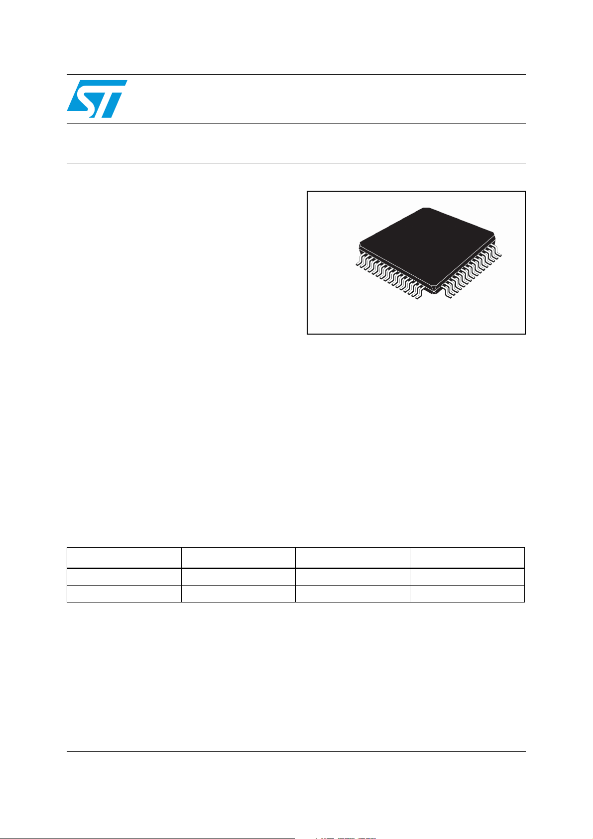
STA321
LQFP-64 package
with exposed pad down (EPD)
Digital gain/attenuation -105 dB to +36 dB in
0.5-dB steps
Soft volume update and muting
DC-blocking selectable high-pass filter
Selectable de-emphasis filter
Up to 13 28-bit user programmable biquads
(EQ) per channel
Bass/treble tone control
Ternary, binary or phase shift modulation
PWM output
Headphone output with jack detector
2
I
C control.
Order code Temperature range Package Packaging
STA321 0 to 70 °C LQFP-64 EPD Tray
STA321TR 0 to 70 °C LQFP-64 EPD Tape and reel
October 2009 Doc ID 15351 Rev 3 1/157
www.st.com
1

Contents STA321
Contents
1 Overview . . . . . . . . . . . . . . . . . . . . . . . . . . . . . . . . . . . . . . . . . . . . . . . . . . 9
2 Pin description . . . . . . . . . . . . . . . . . . . . . . . . . . . . . . . . . . . . . . . . . . . . 10
3 Electrical specifications . . . . . . . . . . . . . . . . . . . . . . . . . . . . . . . . . . . . . 13
3.1 Absolute maximum ratings . . . . . . . . . . . . . . . . . . . . . . . . . . . . . . . . . . . . 13
3.2 Recommended operating conditions . . . . . . . . . . . . . . . . . . . . . . . . . . . . 13
3.3 Electrical characteristics . . . . . . . . . . . . . . . . . . . . . . . . . . . . . . . . . . . . . . 14
3.4 Embedded crystal oscillator . . . . . . . . . . . . . . . . . . . . . . . . . . . . . . . . . . . 17
3.5 Embedded DC regulator . . . . . . . . . . . . . . . . . . . . . . . . . . . . . . . . . . . . . . 19
4 Power-up and power-down sequences . . . . . . . . . . . . . . . . . . . . . . . . . 20
4.1 Device power-up . . . . . . . . . . . . . . . . . . . . . . . . . . . . . . . . . . . . . . . . . . . . 20
4.2 Software power-down mode . . . . . . . . . . . . . . . . . . . . . . . . . . . . . . . . . . . 21
4.2.1 Configuration example . . . . . . . . . . . . . . . . . . . . . . . . . . . . . . . . . . . . . . 22
4.3 Hardware power-down mode . . . . . . . . . . . . . . . . . . . . . . . . . . . . . . . . . . 23
4.3.1 Mild power-down . . . . . . . . . . . . . . . . . . . . . . . . . . . . . . . . . . . . . . . . . . 25
4.3.2 Full power-down . . . . . . . . . . . . . . . . . . . . . . . . . . . . . . . . . . . . . . . . . . . 27
5 Clock management . . . . . . . . . . . . . . . . . . . . . . . . . . . . . . . . . . . . . . . . . 29
5.1 System clock . . . . . . . . . . . . . . . . . . . . . . . . . . . . . . . . . . . . . . . . . . . . . . 30
5.1.1 Configuration example . . . . . . . . . . . . . . . . . . . . . . . . . . . . . . . . . . . . . . 30
5.2 Peripheral clock manager . . . . . . . . . . . . . . . . . . . . . . . . . . . . . . . . . . . . . 31
5.3 Fractional PLL . . . . . . . . . . . . . . . . . . . . . . . . . . . . . . . . . . . . . . . . . . . . . 31
5.3.1 PLL block description . . . . . . . . . . . . . . . . . . . . . . . . . . . . . . . . . . . . . . . 31
5.3.2 Output frequency computation . . . . . . . . . . . . . . . . . . . . . . . . . . . . . . . . 32
6 Digital processing stage . . . . . . . . . . . . . . . . . . . . . . . . . . . . . . . . . . . . . 34
6.1 Signal processing flow . . . . . . . . . . . . . . . . . . . . . . . . . . . . . . . . . . . . . . . 34
6.2 Sampling rate converter . . . . . . . . . . . . . . . . . . . . . . . . . . . . . . . . . . . . . . 35
6.3 Pre-EQ mix 1 and post-EQ mix . . . . . . . . . . . . . . . . . . . . . . . . . . . . . . . . 36
6.3.1 Presets . . . . . . . . . . . . . . . . . . . . . . . . . . . . . . . . . . . . . . . . . . . . . . . . . . 37
6.4 Pre scaler . . . . . . . . . . . . . . . . . . . . . . . . . . . . . . . . . . . . . . . . . . . . . . . . . 37
2/157 Doc ID 15351 Rev 3

STA321 Contents
6.4.1 Presets . . . . . . . . . . . . . . . . . . . . . . . . . . . . . . . . . . . . . . . . . . . . . . . . . . 37
6.5 Equalization, tone control and effects . . . . . . . . . . . . . . . . . . . . . . . . . . . 37
6.6 Biquads . . . . . . . . . . . . . . . . . . . . . . . . . . . . . . . . . . . . . . . . . . . . . . . . . . 39
6.6.1 Presets . . . . . . . . . . . . . . . . . . . . . . . . . . . . . . . . . . . . . . . . . . . . . . . . . . 39
6.7 High-pass filter . . . . . . . . . . . . . . . . . . . . . . . . . . . . . . . . . . . . . . . . . . . . . 39
6.8 Deemphasis filter . . . . . . . . . . . . . . . . . . . . . . . . . . . . . . . . . . . . . . . . . . . 40
6.9 Bass and treble control . . . . . . . . . . . . . . . . . . . . . . . . . . . . . . . . . . . . . . . 41
6.9.1 Configuration example . . . . . . . . . . . . . . . . . . . . . . . . . . . . . . . . . . . . . . 42
6.10 Programmable delay . . . . . . . . . . . . . . . . . . . . . . . . . . . . . . . . . . . . . . . . 42
6.10.1 Presets . . . . . . . . . . . . . . . . . . . . . . . . . . . . . . . . . . . . . . . . . . . . . . . . . . 42
6.11 Volume and mute control . . . . . . . . . . . . . . . . . . . . . . . . . . . . . . . . . . . . . 42
6.12 Limiter (clamping) . . . . . . . . . . . . . . . . . . . . . . . . . . . . . . . . . . . . . . . . . . . 43
6.13 FFX channel re-mapping . . . . . . . . . . . . . . . . . . . . . . . . . . . . . . . . . . . . . 43
6.14 Memory programming . . . . . . . . . . . . . . . . . . . . . . . . . . . . . . . . . . . . . . . 44
6.14.1 Writing one coefficient/location to RAM . . . . . . . . . . . . . . . . . . . . . . . . . 44
6.14.2 Writing a set of five coefficients/locations to RAM . . . . . . . . . . . . . . . . . 45
6.14.3 Reading a set of five coefficients/locations from RAM . . . . . . . . . . . . . . 46
6.14.4 RAM mapping . . . . . . . . . . . . . . . . . . . . . . . . . . . . . . . . . . . . . . . . . . . . 47
7 FFX . . . . . . . . . . . . . . . . . . . . . . . . . . . . . . . . . . . . . . . . . . . . . . . . . . . . . . 52
7.1 Functional description . . . . . . . . . . . . . . . . . . . . . . . . . . . . . . . . . . . . . . . 52
7.2 Modulation schemes . . . . . . . . . . . . . . . . . . . . . . . . . . . . . . . . . . . . . . . . 52
7.3 PWM shift feature . . . . . . . . . . . . . . . . . . . . . . . . . . . . . . . . . . . . . . . . . . . 55
7.4 Ternary mode . . . . . . . . . . . . . . . . . . . . . . . . . . . . . . . . . . . . . . . . . . . . . . 56
7.5 Minimum pulse limitation . . . . . . . . . . . . . . . . . . . . . . . . . . . . . . . . . . . . . 56
7.6 Headphone modulation . . . . . . . . . . . . . . . . . . . . . . . . . . . . . . . . . . . . . . 57
7.7 pfStart™ operation . . . . . . . . . . . . . . . . . . . . . . . . . . . . . . . . . . . . . . . . . . 58
7.8 PWM00 output . . . . . . . . . . . . . . . . . . . . . . . . . . . . . . . . . . . . . . . . . . . . . 59
8 CMOS power stage . . . . . . . . . . . . . . . . . . . . . . . . . . . . . . . . . . . . . . . . . 60
9 Fault detection and recovery . . . . . . . . . . . . . . . . . . . . . . . . . . . . . . . . . 63
9.1 External amplifier . . . . . . . . . . . . . . . . . . . . . . . . . . . . . . . . . . . . . . . . . . . 63
9.2 CMOS bridge . . . . . . . . . . . . . . . . . . . . . . . . . . . . . . . . . . . . . . . . . . . . . . 63
Doc ID 15351 Rev 3 3/157

Contents STA321
10 ADC . . . . . . . . . . . . . . . . . . . . . . . . . . . . . . . . . . . . . . . . . . . . . . . . . . . . . . 64
10.1 Description . . . . . . . . . . . . . . . . . . . . . . . . . . . . . . . . . . . . . . . . . . . . . . . . 64
10.2 Application schematic . . . . . . . . . . . . . . . . . . . . . . . . . . . . . . . . . . . . . . . . 65
10.2.1 Configuration example . . . . . . . . . . . . . . . . . . . . . . . . . . . . . . . . . . . . . . 65
11 Serial audio interface . . . . . . . . . . . . . . . . . . . . . . . . . . . . . . . . . . . . . . . 66
11.1 Master mode . . . . . . . . . . . . . . . . . . . . . . . . . . . . . . . . . . . . . . . . . . . . . . 66
11.2 Slave mode . . . . . . . . . . . . . . . . . . . . . . . . . . . . . . . . . . . . . . . . . . . . . . . 67
11.3 Serial formats . . . . . . . . . . . . . . . . . . . . . . . . . . . . . . . . . . . . . . . . . . . . . . 68
11.3.1 Right justified . . . . . . . . . . . . . . . . . . . . . . . . . . . . . . . . . . . . . . . . . . . . . 68
11.3.2 Left justified . . . . . . . . . . . . . . . . . . . . . . . . . . . . . . . . . . . . . . . . . . . . . . 68
11.3.3 DSP . . . . . . . . . . . . . . . . . . . . . . . . . . . . . . . . . . . . . . . . . . . . . . . . . . . . 69
11.3.4 I
11.3.5 PCM/IF (non-delayed mode) . . . . . . . . . . . . . . . . . . . . . . . . . . . . . . . . . 69
11.3.6 PCM/IF (delayed mode) . . . . . . . . . . . . . . . . . . . . . . . . . . . . . . . . . . . . . 70
2
S . . . . . . . . . . . . . . . . . . . . . . . . . . . . . . . . . . . . . . . . . . . . . . . . . . . . . 69
11.4 Invalid detection . . . . . . . . . . . . . . . . . . . . . . . . . . . . . . . . . . . . . . . . . . . . 71
12 Headphone detection . . . . . . . . . . . . . . . . . . . . . . . . . . . . . . . . . . . . . . . 72
12.1 Applications circuits . . . . . . . . . . . . . . . . . . . . . . . . . . . . . . . . . . . . . . . . . 73
12.2 Configuration example . . . . . . . . . . . . . . . . . . . . . . . . . . . . . . . . . . . . . . . 74
13 I2C interface . . . . . . . . . . . . . . . . . . . . . . . . . . . . . . . . . . . . . . . . . . . . . . . 75
13.1 Communication protocol . . . . . . . . . . . . . . . . . . . . . . . . . . . . . . . . . . . . . . 75
13.1.1 Data transition and change . . . . . . . . . . . . . . . . . . . . . . . . . . . . . . . . . . 75
13.1.2 Start condition . . . . . . . . . . . . . . . . . . . . . . . . . . . . . . . . . . . . . . . . . . . . 75
13.1.3 Stop condition . . . . . . . . . . . . . . . . . . . . . . . . . . . . . . . . . . . . . . . . . . . . 75
13.1.4 Data input . . . . . . . . . . . . . . . . . . . . . . . . . . . . . . . . . . . . . . . . . . . . . . . 75
13.1.5 Device addressing . . . . . . . . . . . . . . . . . . . . . . . . . . . . . . . . . . . . . . . . . 75
13.1.6 Write operation . . . . . . . . . . . . . . . . . . . . . . . . . . . . . . . . . . . . . . . . . . . 75
13.1.7 Read operation . . . . . . . . . . . . . . . . . . . . . . . . . . . . . . . . . . . . . . . . . . . 76
14 Register description . . . . . . . . . . . . . . . . . . . . . . . . . . . . . . . . . . . . . . . . 77
15 I2C disabled (microless) mode . . . . . . . . . . . . . . . . . . . . . . . . . . . . . . 150
16 Package mechanical data . . . . . . . . . . . . . . . . . . . . . . . . . . . . . . . . . . . 152
4/157 Doc ID 15351 Rev 3

STA321 Contents
17 Glossary . . . . . . . . . . . . . . . . . . . . . . . . . . . . . . . . . . . . . . . . . . . . . . . . . 154
18 Trademarks and other acknowledgements . . . . . . . . . . . . . . . . . . . . . 155
19 Revision history . . . . . . . . . . . . . . . . . . . . . . . . . . . . . . . . . . . . . . . . . . 156
Doc ID 15351 Rev 3 5/157

List of tables STA321
List of tables
Table 1. Device summary . . . . . . . . . . . . . . . . . . . . . . . . . . . . . . . . . . . . . . . . . . . . . . . . . . . . . . . . . . 1
Table 2. Pin list . . . . . . . . . . . . . . . . . . . . . . . . . . . . . . . . . . . . . . . . . . . . . . . . . . . . . . . . . . . . . . . . . 10
Table 3. Power supply pin list . . . . . . . . . . . . . . . . . . . . . . . . . . . . . . . . . . . . . . . . . . . . . . . . . . . . . . 12
Table 4. Absolute maximum ratings . . . . . . . . . . . . . . . . . . . . . . . . . . . . . . . . . . . . . . . . . . . . . . . . . 13
Table 5. Recommended operating conditions . . . . . . . . . . . . . . . . . . . . . . . . . . . . . . . . . . . . . . . . . 13
Table 6. Electrical specifications. . . . . . . . . . . . . . . . . . . . . . . . . . . . . . . . . . . . . . . . . . . . . . . . . . . . 14
Table 7. Oscillator specifications . . . . . . . . . . . . . . . . . . . . . . . . . . . . . . . . . . . . . . . . . . . . . . . . . . . 18
Table 8. Power-up signal description . . . . . . . . . . . . . . . . . . . . . . . . . . . . . . . . . . . . . . . . . . . . . . . . 20
Table 9. Startup timings . . . . . . . . . . . . . . . . . . . . . . . . . . . . . . . . . . . . . . . . . . . . . . . . . . . . . . . . . . 21
Table 10. Configuration example . . . . . . . . . . . . . . . . . . . . . . . . . . . . . . . . . . . . . . . . . . . . . . . . . . . . 21
Table 11. Registers for power-down. . . . . . . . . . . . . . . . . . . . . . . . . . . . . . . . . . . . . . . . . . . . . . . . . . 21
Table 12. Example configurations for power-down. . . . . . . . . . . . . . . . . . . . . . . . . . . . . . . . . . . . . . . 22
Table 13. Frequently used signals . . . . . . . . . . . . . . . . . . . . . . . . . . . . . . . . . . . . . . . . . . . . . . . . . . . 24
Table 14. Clock control registers . . . . . . . . . . . . . . . . . . . . . . . . . . . . . . . . . . . . . . . . . . . . . . . . . . . . 29
Table 15. Clock characteristics. . . . . . . . . . . . . . . . . . . . . . . . . . . . . . . . . . . . . . . . . . . . . . . . . . . . . . 30
Table 16. Register setup to provide sys_clk from MCLK to PLL. . . . . . . . . . . . . . . . . . . . . . . . . . . . . 30
Table 17. Input division factor (IDF) . . . . . . . . . . . . . . . . . . . . . . . . . . . . . . . . . . . . . . . . . . . . . . . . . . 32
Table 18. Loop division factor (LDF). . . . . . . . . . . . . . . . . . . . . . . . . . . . . . . . . . . . . . . . . . . . . . . . . . 33
Table 19. Channel mapping . . . . . . . . . . . . . . . . . . . . . . . . . . . . . . . . . . . . . . . . . . . . . . . . . . . . . . . . 36
Table 20. EQ control signals. . . . . . . . . . . . . . . . . . . . . . . . . . . . . . . . . . . . . . . . . . . . . . . . . . . . . . . . 38
Table 21. Selecting EQ curves . . . . . . . . . . . . . . . . . . . . . . . . . . . . . . . . . . . . . . . . . . . . . . . . . . . . . . 42
Table 22. RAM mapping for processing stage . . . . . . . . . . . . . . . . . . . . . . . . . . . . . . . . . . . . . . . . . . 47
Table 23. Modulation type with register programming . . . . . . . . . . . . . . . . . . . . . . . . . . . . . . . . . . . . 54
Table 24. CMOS bridge signal descriptions . . . . . . . . . . . . . . . . . . . . . . . . . . . . . . . . . . . . . . . . . . . . 60
Table 25. Power output (at 1% THD) in headphone mode . . . . . . . . . . . . . . . . . . . . . . . . . . . . . . . . . 61
Table 26. Logic circuit at bridge input . . . . . . . . . . . . . . . . . . . . . . . . . . . . . . . . . . . . . . . . . . . . . . . . . 62
Table 27. Example register settings for ADC . . . . . . . . . . . . . . . . . . . . . . . . . . . . . . . . . . . . . . . . . . . 65
Table 28. Timing parameters for master mode. . . . . . . . . . . . . . . . . . . . . . . . . . . . . . . . . . . . . . . . . . 67
Table 29. Timing parameters for slave mode . . . . . . . . . . . . . . . . . . . . . . . . . . . . . . . . . . . . . . . . . . . 67
Table 30. Headphone 1 detector . . . . . . . . . . . . . . . . . . . . . . . . . . . . . . . . . . . . . . . . . . . . . . . . . . . . 72
Table 31. Headphone 2 detector . . . . . . . . . . . . . . . . . . . . . . . . . . . . . . . . . . . . . . . . . . . . . . . . . . . . 72
Table 32. Headphone detection configuration sequence for binary SE . . . . . . . . . . . . . . . . . . . . . . . 74
Table 33. Headphone detection configuration sequence for binary headphone . . . . . . . . . . . . . . . . 74
Table 34. Register summary. . . . . . . . . . . . . . . . . . . . . . . . . . . . . . . . . . . . . . . . . . . . . . . . . . . . . . . . 77
Table 35. Bass/treble filter gains used in register addresses 0x78 - 0x7F . . . . . . . . . . . . . . . . . . . . 115
Table 36. LQFP-64L EPD dimensions . . . . . . . . . . . . . . . . . . . . . . . . . . . . . . . . . . . . . . . . . . . . . . . 153
Table 37. Document revision history . . . . . . . . . . . . . . . . . . . . . . . . . . . . . . . . . . . . . . . . . . . . . . . . 156
6/157 Doc ID 15351 Rev 3

STA321 List of figures
List of figures
Figure 1. STA321 block diagram . . . . . . . . . . . . . . . . . . . . . . . . . . . . . . . . . . . . . . . . . . . . . . . . . . . . 9
Figure 2. Pin out . . . . . . . . . . . . . . . . . . . . . . . . . . . . . . . . . . . . . . . . . . . . . . . . . . . . . . . . . . . . . . . . 10
Figure 3. Test circuit . . . . . . . . . . . . . . . . . . . . . . . . . . . . . . . . . . . . . . . . . . . . . . . . . . . . . . . . . . . . . 17
Figure 4. Oscillator configuration . . . . . . . . . . . . . . . . . . . . . . . . . . . . . . . . . . . . . . . . . . . . . . . . . . . 17
Figure 5. Equivalent circuit of crystal and external components . . . . . . . . . . . . . . . . . . . . . . . . . . . . 18
Figure 6. Embedded DC regulator scheme . . . . . . . . . . . . . . . . . . . . . . . . . . . . . . . . . . . . . . . . . . . 19
Figure 7. Startup sequence . . . . . . . . . . . . . . . . . . . . . . . . . . . . . . . . . . . . . . . . . . . . . . . . . . . . . . . . 20
Figure 8. Hardware power-done sequence . . . . . . . . . . . . . . . . . . . . . . . . . . . . . . . . . . . . . . . . . . . . 23
Figure 9. Hardware powerdown sequence (mild mode) . . . . . . . . . . . . . . . . . . . . . . . . . . . . . . . . . . 26
Figure 10. Hardware power-down sequence (full mode) . . . . . . . . . . . . . . . . . . . . . . . . . . . . . . . . . . . 28
Figure 11. Clock management scheme . . . . . . . . . . . . . . . . . . . . . . . . . . . . . . . . . . . . . . . . . . . . . . . 29
Figure 12. PLL block diagram . . . . . . . . . . . . . . . . . . . . . . . . . . . . . . . . . . . . . . . . . . . . . . . . . . . . . . . 31
Figure 13. Processing flow . . . . . . . . . . . . . . . . . . . . . . . . . . . . . . . . . . . . . . . . . . . . . . . . . . . . . . . . . 34
Figure 14. Processing data multiplexer . . . . . . . . . . . . . . . . . . . . . . . . . . . . . . . . . . . . . . . . . . . . . . . . 34
Figure 15. SAI_out data multiplexer . . . . . . . . . . . . . . . . . . . . . . . . . . . . . . . . . . . . . . . . . . . . . . . . . . 35
Figure 16. Sample rate converter block diagram . . . . . . . . . . . . . . . . . . . . . . . . . . . . . . . . . . . . . . . . 35
Figure 17. Mixers block diagram . . . . . . . . . . . . . . . . . . . . . . . . . . . . . . . . . . . . . . . . . . . . . . . . . . . . . 36
Figure 18. EQ/tone block diagram . . . . . . . . . . . . . . . . . . . . . . . . . . . . . . . . . . . . . . . . . . . . . . . . . . . 37
Figure 19. Biquad coefficient selection . . . . . . . . . . . . . . . . . . . . . . . . . . . . . . . . . . . . . . . . . . . . . . . . 38
Figure 20. Biquad filter . . . . . . . . . . . . . . . . . . . . . . . . . . . . . . . . . . . . . . . . . . . . . . . . . . . . . . . . . . . . 39
Figure 21. High-pass filter frequency response . . . . . . . . . . . . . . . . . . . . . . . . . . . . . . . . . . . . . . . . . 39
Figure 22. Deemphasis filter frequency response . . . . . . . . . . . . . . . . . . . . . . . . . . . . . . . . . . . . . . . 40
Figure 23. Frequency responses of treble control at 1-dB gain steps . . . . . . . . . . . . . . . . . . . . . . . . . 41
Figure 24. Frequency responses of bass control at 1-dB gain steps . . . . . . . . . . . . . . . . . . . . . . . . . . 41
Figure 25. FFX re-mapping . . . . . . . . . . . . . . . . . . . . . . . . . . . . . . . . . . . . . . . . . . . . . . . . . . . . . . . . . 43
Figure 26. Writing RAM location . . . . . . . . . . . . . . . . . . . . . . . . . . . . . . . . . . . . . . . . . . . . . . . . . . . . . 44
Figure 27. Writing five contiguous RAM locations . . . . . . . . . . . . . . . . . . . . . . . . . . . . . . . . . . . . . . . 45
Figure 28. Reading five contiguous RAM locations . . . . . . . . . . . . . . . . . . . . . . . . . . . . . . . . . . . . . . 46
Figure 29. FFX processing schematic . . . . . . . . . . . . . . . . . . . . . . . . . . . . . . . . . . . . . . . . . . . . . . . . 52
Figure 30. PWM modes for outputs A and B . . . . . . . . . . . . . . . . . . . . . . . . . . . . . . . . . . . . . . . . . . . 53
Figure 31. Modulation waveforms corresponding to Table 23 . . . . . . . . . . . . . . . . . . . . . . . . . . . . . . 54
Figure 32. New phase shift modulation with shift feature . . . . . . . . . . . . . . . . . . . . . . . . . . . . . . . . . . 55
Figure 33. Ternary modulation . . . . . . . . . . . . . . . . . . . . . . . . . . . . . . . . . . . . . . . . . . . . . . . . . . . . . . 56
Figure 34. Modulation for headphones . . . . . . . . . . . . . . . . . . . . . . . . . . . . . . . . . . . . . . . . . . . . . . . . 57
Figure 35. Digital pop-free ramp implementation . . . . . . . . . . . . . . . . . . . . . . . . . . . . . . . . . . . . . . . . 58
Figure 36. CMOS half bridge block diagram . . . . . . . . . . . . . . . . . . . . . . . . . . . . . . . . . . . . . . . . . . . . 60
Figure 37. Analog pop-free schematic . . . . . . . . . . . . . . . . . . . . . . . . . . . . . . . . . . . . . . . . . . . . . . . . 61
Figure 38. Analog pop-free start-up and switch-off sequence . . . . . . . . . . . . . . . . . . . . . . . . . . . . . . 62
Figure 39. ADC front-end block diagram . . . . . . . . . . . . . . . . . . . . . . . . . . . . . . . . . . . . . . . . . . . . . . 64
Figure 40. Typical connections for power supplies and inputs . . . . . . . . . . . . . . . . . . . . . . . . . . . . . . 65
Figure 41. SAI typical sampling rates . . . . . . . . . . . . . . . . . . . . . . . . . . . . . . . . . . . . . . . . . . . . . . . . . 66
Figure 42. Timing diagram for master mode . . . . . . . . . . . . . . . . . . . . . . . . . . . . . . . . . . . . . . . . . . . . 66
Figure 43. Timing diagram for slave mode . . . . . . . . . . . . . . . . . . . . . . . . . . . . . . . . . . . . . . . . . . . . . 67
Figure 44. Right justified serial format . . . . . . . . . . . . . . . . . . . . . . . . . . . . . . . . . . . . . . . . . . . . . . . . 68
Figure 45. Left justified serial format . . . . . . . . . . . . . . . . . . . . . . . . . . . . . . . . . . . . . . . . . . . . . . . . . . 68
Figure 46. DSP serial format . . . . . . . . . . . . . . . . . . . . . . . . . . . . . . . . . . . . . . . . . . . . . . . . . . . . . . . . 69
Figure 47. I
Figure 48. PCM (non-delayed) serial format . . . . . . . . . . . . . . . . . . . . . . . . . . . . . . . . . . . . . . . . . . . . 69
2
S serial format . . . . . . . . . . . . . . . . . . . . . . . . . . . . . . . . . . . . . . . . . . . . . . . . . . . . . . . . . 69
Doc ID 15351 Rev 3 7/157

List of figures STA321
Figure 49. PCM (delayed) serial format . . . . . . . . . . . . . . . . . . . . . . . . . . . . . . . . . . . . . . . . . . . . . . . 70
Figure 50. Invalid input detection schematic . . . . . . . . . . . . . . . . . . . . . . . . . . . . . . . . . . . . . . . . . . . . 71
Figure 51. Headphone detection circuit for single-ended configuration . . . . . . . . . . . . . . . . . . . . . . . 73
Figure 52. Headphone detection circuit for binary HP configuration . . . . . . . . . . . . . . . . . . . . . . . . . . 73
Figure 53. I
Figure 54. I
2
C write operations . . . . . . . . . . . . . . . . . . . . . . . . . . . . . . . . . . . . . . . . . . . . . . . . . . . . . . 76
2
C read operations . . . . . . . . . . . . . . . . . . . . . . . . . . . . . . . . . . . . . . . . . . . . . . . . . . . . . . 76
Figure 55. Microless mode block diagram . . . . . . . . . . . . . . . . . . . . . . . . . . . . . . . . . . . . . . . . . . . . 150
Figure 56. LQFP-64L EPD outline drawing . . . . . . . . . . . . . . . . . . . . . . . . . . . . . . . . . . . . . . . . . . . . 152
8/157 Doc ID 15351 Rev 3
STA321 Overview
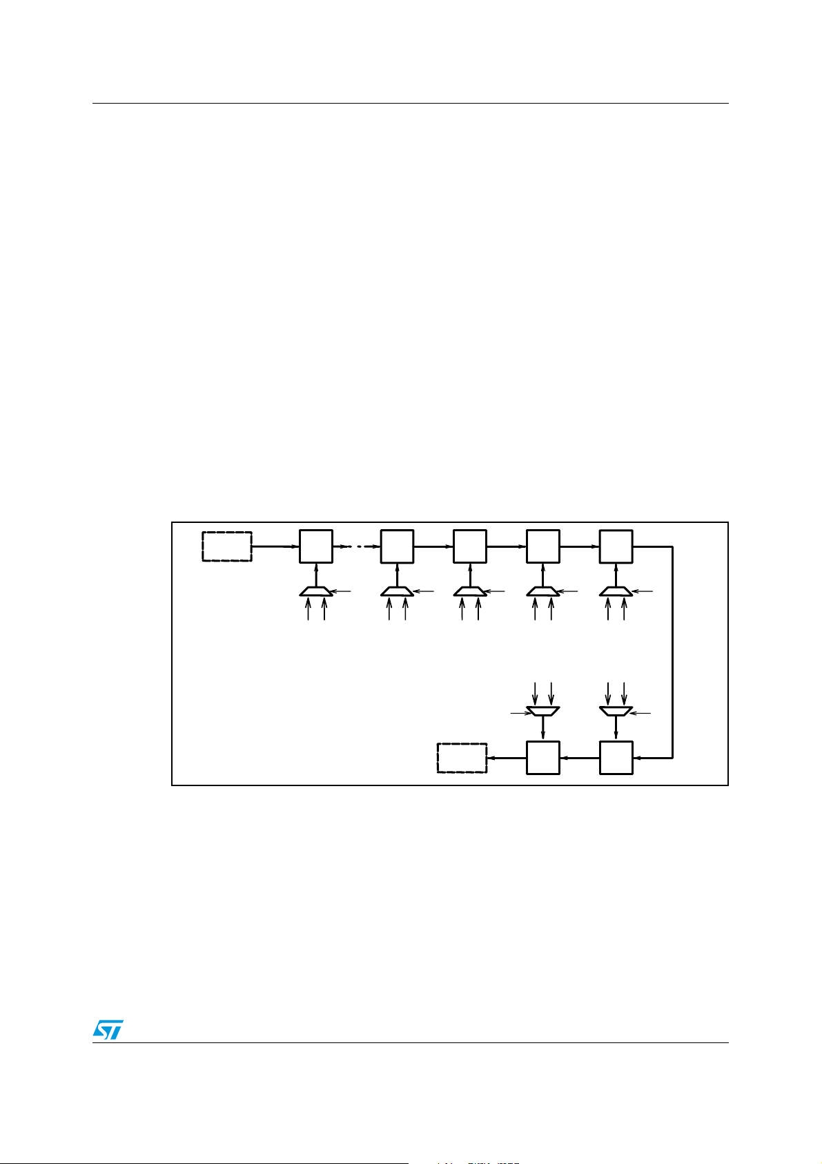
1 Overview
The STA321 is a single chip solution for digital audio processing applications of up to
4.0 channels.
The STA321 is part of the Sound Terminal™ family that together with the digital power stage
provides full digital audio streaming to the speaker, offering cost effectiveness, low energy
dissipation and sound enrichment.
The STA321 input section consists of two multiplexed stereo analog inputs, a 16-bit ADC
and two independent digital input interfaces. The serial audio data input interface accepts all
possible formats, including the popular I
by the ADC or by the digitally processed signals.
The device has a full assortment of digital processing features. This includes sample rate
converter, pre and post mixing, up to 13 programmable 28-bit biquads (EQ) per channel,
bass/treble tone control and DRC. The embedded headphone detector indicates when
headphone jack is inserted.
The STA321 provides four independent channels of FFX™ output capabilities. In
conjunction with a power device, it provides high-quality, high-efficiency, all digital
amplification.
2
S format. There is also a digital output interface fed
The embedded CMOS bridge supplies up to 0.5 W into an 8-Ω load and 70 mW into a 16-Ω
load for the headphones output.
Figure 1. STA321 block diagram
SDATAO1
BICLKO
LRCLKO
SDATAO2
Serial audio
Osc
interface
4-channel
SRC
XTI
XTO
PLL
pre mixer
MCLK
V_BIAS
VCM
VHI
VLO
BICLKI1
LRCLKI1
SDATAI1
BICLKI2
LRCLKI2
SDATAI2
INL1
INL2
INR1
INR2
HPDET
Bias
Serial audio
interface
Serial audio
interface
PGA
PGA
HP detection
.
ADC
RSTN
Pre scaler
Divider
CLKOUT
STBY
Equalizer
TM
EAFTN
EATSN
EAPDN
Delay
13 biquad filters
Post mixer
Volume control and
saturation
FFX™
modulator
CMOS
headphone
bridge
EAPWM4
EAPWM3
EAPWM2
EAPWM1
OUT1
OUT2
OUT3
PWM00
I2C interface
SCL
MUTE
SDA
I2CDIS
ACLK
REG_BYP
Doc ID 15351 Rev 3 9/157
Pin description STA321
2 Pin description
Figure 2. Pin out
BICLKO
BICLKI1
BICLKI2
LRCLKO
LRCLKI1
LRCLKI2
SDATAO1
SDATAO2
SDATAI1
SDATAI2
MCLK
XTI
XTO
NC
PGND
PVDD
64
63
62
61
SCL
VCC1
OUT1
GND1
GND2
OUT2
VCC2
VCC3
OUT3
GND3
NC
PWM00
NC
HPDET
GND33
VCC33
1
2
3
4
5
6
7
8
9
10
11
12
13
14
15
16
17
18
605958
19
20
21
57
56
STA321
22
23
24
25
55
54
53
52
51
50
49
48
TM
47
VDDIO2
46
VDD_REG2
45
DGND2
44
I2CDIS
43
ACLK
42
EAPDN
41
EATSN
40
EAFTN
39
EAPWM1
38
EAPWM2
37
EAPWM3
36
EAPWM4
35
STBY
34
RSTN
33
26
27
28
29
30
31
32
INL1
SDA
MUTE
CLKOUT
Table 2. Pin list
Pin Pull Name Type Description
1 - SCL In (digital), schmitt tr I
3 - OUT1 Out (analog) HP/line-out PWM 1
6 - OUT2 Out (analog) HP/line-out PWM 2
9 - OUT3 Out (analog) HP/line-out PWM 3
11 - NC - Not connected
10/157 Doc ID 15351 Rev 3
12 - PWM00 Out (digital) Auxiliary PWM
13 - NC - Not connected
14 - HPDET In (analog) Headphone detection
DGND1
REG_BYP
VDD_REG1
AGND
V_BIAS
VDDIO1
VHI
VLO
2
C serial clock, schmitt trigger input
AVDD
INR1
VCM
INR2
INL2
STA321 Pin description
Table 2. Pin list (continued)
Pin Pull Name Type Description
17 - CLKOUT Out (digital) Buffered clock output
18 - SDA In/Out (digital) I
19 H MUTE In (digital) Mute (active high)
21 - REG_BYPASS In (analog)
24 - BIAS In/Out (analog) ADC microphone bias voltage
26 - VLO In (analog) ADC low reference voltage
27 - VHI In (analog) ADC high reference voltage
29 - INR1 In/Out (analog) ADC right channel line input1
30 - INR2 In/Out (analog) ADC right channel line input2
31 - VCM In/Out (analog) ADC common mode voltage
32 - INL2 In (analog) ADC left channel line input2 or microphone input2
33 - INL1 In (analog) ADC left channel line input1 or microphone input1
2
C serial data
DC regulator bypass:
0: normal operation, regulator enabled
1: regulator bypassed
Reset:
34 H RSTN In (digital)
0: reset state
1: normal operation
Standby mode:
35 - STBY In (digital)
0: normal operation
1: power-down
36 - EAPWM4 Out (digital) External amplifier PWM 4B
37 - EAPWM3 Out (digital) External amplifier PWM 4A
38 - EAPWM2 Out (digital) External amplifier PWM 3B
39 - EAPWM1 Out (digital) External amplifier PWM 3A
External power fault signal:
40 H EAFTN Out (digital)
0: fault
1: normal operational mode
External amplifier control:
41 - EATSN Out (digital)
0: active
1: 3-state
42 - EAPDN Out (digital) External amplifier powerdown (active low)
43 - ACLK In (digital), schmitt tr Reserved pin, connect to ground
2
C disable:
I
44 L I2CDIS In (digital)
2
C enabled
0: I
1: I2C disabled
48 L TM In (digital)
Test mode:
0: normal operation
51 - NC - Not connected
Doc ID 15351 Rev 3 11/157
Pin description STA321
Table 2. Pin list (continued)
Pin Pull Name Type Description
52 - XTO Out (digital), 1.8 V Crystal output
53 - XTI In (digital), 1.8 V Crystal input or master clock input
54 - MCLK In (digital), schmitt tr Master clock input 3.3-V compatible, schmitt input
55 - SDATAI2 In (digital) Input serial audio interface data
56 - SDATAI1 In (digital) Input serial audio interface data
57 - SDATAO2 Out (digital) Output serial audio interface data
58 - SDATAO1 Out (digital) Output serial audio interface data
59 - LRCLKI2 In/Out (digital) Input serial audio interface L/R-clock
60 - LRCLKI1 In/Out (digital) Input serial audio interface L/R-clock
61 - LRCLKO In/Out (digital)
62 - BICLKI2 In/Out (digital) Input serial audio interface bit clock
63 - BICLKI1 In/Out (digital) Input serial audio interface bit clock
64 - BICLKO In/Out (digital)
Output serial audio interface L/R-clock
(volume DOWN when I2CDIS=1)
Output serial audio interface bit clock
(volume UP when I2CDIS=1)
Table 3. Power supply pin list
Number Name Type Description
2 VCC1 Supply CMOS bridge channel 1 supply
4 GND1 Ground CMOS bridge channel 1 ground
5 GND2 Ground CMOS bridge channel 2 ground
7 VCC2 Supply CMOS bridge channel 2 supply
8 VCC3 Supply CMOS bridge channel 3 supply
10 GND3 Ground CMOS bridge channel 3 ground
15 GND33 Ground CMOS bridge level shifter ground
16 VCC33 Supply CMOS bridge level shifter supply
20 DGND1 Ground Digital ground
22 VDD_REG1 Supply DC regulator unit supply
23 VDDIO1 Supply 3.3-V IO supply
25 AGND Ground ADC analog ground
28 AVDD Supply ADC analog supply
45 DGND2 Ground Digital ground
46 VDD_REG2 Supply DC regulator unit supply
47 VDDIO2 Supply 3.3-V IO supply
49 PVDD Supply PLL analog supply
50 PGND Ground PLL analog ground
12/157 Doc ID 15351 Rev 3
STA321 Electrical specifications
3 Electrical specifications
3.1 Absolute maximum ratings
Table 4. Absolute maximum ratings
Pin name/Symbol Parameter Negative Positive Unit
VDD_REG1,
VDD_REG2
Digital supply voltage -0.3 4.0 V
VDDIO1, VDDIO2 Digital IO supply voltage -0.3 4.0 V
PVDD PLL analog supply voltage -0.3 4.0 V
AVDD ADC analog supply voltage -0.3 4.0 V
VCC1, VCC2, VCC3 CMOS bridge supply voltage -0.3 4.0 V
VCC33 CMOS bridge level shifter power supply -0.3 4.0 V
T
T
STG
OP
Storage temperature -40 150 °C
Operating junction temperature -20 125 °C
Note: All grounds must always be within 0.3 V of each other.
3.2 Recommended operating conditions
Table 5. Recommended operating conditions
Symbol Parameter Min Typ Max Unit
V
VDD_REG1
V
VDD_REG2
V
PVDD
V
AVD D
V
VCC1
V
VCC3
V
VCC33
V
VDDIO1
V
IH
V
IL
T
amb
, V
VCC2
, V
,
,
VDDIO2
Digital supply voltage 2.5 3.3 3.6 V
PLL analog supply voltage 2.5 3.3 3.6 V
ADC analog supply voltage 1.8 3.3 3.6 V
CMOS bridge supply voltage 1.55 - 3.3 V
CMOS bridge level shifter power supply.
Ensure that V
VCC33
<= V
3.3-V IO supply 2.7 3.3 3.6 V
High input voltage, 1.8-V pads 1.3 - -
High input voltage, 3.3-V pads 2.0 - -
Low input voltage, 1.8-V pads - - 0.6
Low input voltage, 3.3-V pads - - 0.8
Ambient temperature 0 - 70 °C
VCCx
always
1.55 - 3.3 V
V
V
Doc ID 15351 Rev 3 13/157
Electrical specifications STA321
3.3 Electrical characteristics
Unless otherwise specified, the results in Table 6 below are given for the operating
conditions V
to default conditions.
Table 6. Electrical specifications
Symbol Parameter Test conditions Min Typ Max Unit
General
V
OH
V
OL
V
hys
R
UP
R
DN
I
STBYIO
High output voltage, 1.8-V pads - 1.4 - -
High output voltage, 3.3-V pads -
Low output voltage, 1.8-V pads IOL = 2 mA --0.15
Low output voltage, 3.3-V pads I
Schmitt trigger hysteresis, 3.3-V IO - - 0.4 - V
Pull-up resistance - - 50 - kΩ
Pull-down resistance - - 50 - kΩ
Standby current, pins VDDIO1,2
=3.3 V, RL = 32 Ω, f
CC
= 12.288 MHz, Tamb = 25 °C and with the PLL set
MCLK
V
VDDIO
- 0.15
= 2 mA --0.15
OL
Pin STBY = 3.3 V
CLKOUT disabled
-450-µA
--
V
V
I
DDIO
I
STBYL0
I
STBYL1
I
DDL1
I
STBYPD
Operating current, pins VDDIO1,2 - - 3 - mA
Standby current, pins VDD_REG1,2
Standby current, pins VDD_REG1,2
Operating current,
pins VDD_REG1,2
Pre-drive supply current in standby,
pin VCC33
Deep power-down,
V
VDD_REG1,2
= 3.3 V
Mild power-down,
V
VDD_REG1,2
f
MCLK
= 3.3 V
= 12.288 MHz, Play
from SAI to CMOS bridge
and EAPWM, f
on SAI_out, V
V
VDD_REG1,2
ADC
AVD D
= 3.3 V
= 48 kHz
= 3.3 V,
- - 4.7 - µA
-450-µA
-2-mA
-45-mA
14/157 Doc ID 15351 Rev 3
STA321 Electrical specifications
Table 6. Electrical specifications (continued)
Symbol Parameter Test conditions Min Typ Max Unit
Amplifier (CMOS bridge)
η Output power efficiency - - 90 - %
Output power in HP mode with
THD = 1%
P
HPOUT
Output power in HP mode with
THD = 10%
SNR Signal to noise ratio 20 Hz to 20 kHz - 75 - dB
3.3-V supply R
3.3-V supply R
= 32 Ω -41-
L
= 32 Ω -53-
L
mW
THD + N Total harmonic distortion plus noise
RL = 32 Ω,
HP mode
0 dBFs In - 0.3 -
%
-6 dBFs In - 0.05 -
DR Dynamic range A-weighted - 80 - dB
I
STBYP
I
DDP
I
DDPD
t
R
t
F
R
DSON
I
OCH
I
OCL
Current in standby, pins VCCx - - 2 - µA
Operating current, pins VCCx
Pre-drive supply current in
operation, pin VCC33
No LC filter, no load,
PWM at 50% duty-cycle
No load,
PWM at 50% duty-cycle
-1-mA
- 250 350 µA
Driver rise time, pins OUT1-3 Resistive load, see Figure 3 -5-ns
Driver fall time, pins OUT1-3 Resistive load, see Figure 3 -5-ns
Headphone output stage N/P MOS
on-resistance
Over-current limit for OUT1-3 to
VCCx short circuit
Over-current limit for OUT1-3 to
ground short circuit
- - 500 700 mΩ
- - 1.88 - A
- - 1.72 - A
PLL
I
STDBYPLL
I
DDPLL
f
CLKIN_Range
Duty
CLKIN
t
CLKIN_RF
f
F_INT
f
VCO_Range
Duty
VCO
T
LOCK
PLL supply current in standby - - 20 - µA
PLL supply current in operation - - 0.4 1.0 mA
Input clock frequency range - 2.048 - 49.152 MHz
Input clock duty cycle - 40 - 60 %
Input clock rise/fall time - - - 0.2 ns
PFD input clock frequency PLL_FR_CTRL = 1 2.048 - 12.288 MHz
Clock out range - 65.536 - 98.304 MHz
Clock out duty cycle - 35 - 65 %
Lock time - - - 200 µs
Doc ID 15351 Rev 3 15/157
Electrical specifications STA321
Table 6. Electrical specifications (continued)
Symbol Parameter Test conditions Min Typ Max Unit
ADC
I
DDA
I
STDBYA
DR Dynamic range
SNR
ADC
THD
ADC
CT Channel cross talk V
- Group delay
Supply current in operating mode V
AVDD supply current in standby V
Signal to noise ratio
Total harmonic distortion
= 3.3V - 10 15 mA
AVD D
= 3.3V - 2 - µA
AVD D
1 kHz, A-weigthed
= 3.3 V
V
AVD D
1 kHz, A-weighted
= 3.3 V
V
AVD D
1 kHz, -1dB
V
= 3.3 V
AVD D
= 3.3 V - 80 - dB
AVD D
Fs mode (f
Fs_by_4 mode (f
= 32 kHz) - 0.4 -
S
= 16 kHz) - 0.7 -
S
= 8 kHz) - 1.4 -
S
-90-dB
-92-dB
-85-dB
msFs_by_2 mode (f
- Pass band - - 0.4535 - Fs
= 44.1 kHz) - 0.08 -
S
-0.08-
-0.08-
= 44.1 kHz) - 45 -
S
-45-
-45-
dB
dB
- Pass band ripple
- Stop band attenuation
Fs mode (f
Fs_by_2 mode
(f
= 22.05 kHz)
S
Fs_by_4 mode
= 11.025 kHz)
(f
S
Fs mode (f
Fs_by_2 mode
(f
= 22.05 kHz)
S
Fs_by_4 mode
= 11.025 kHz)
(f
S
-3 dB - 7 - Hz
- Frequency response
-0.08 dB - 50 - Hz
- Linear phase deviation at 20 Hz - 19.35 - deg
- Pass-band ripple - - 0.08 - dB
Headphone detector threshold limits
HP low threshold - - 2.34 -
E_HP1
HP high threshold - - 2.52 -
HP low threshold - - 0.7 -
E_HP2
HP high threshold - - 0.9 -
16/157 Doc ID 15351 Rev 3
V
V
STA321 Electrical specifications
Figure 3. Test circuit
R = 32 Ω
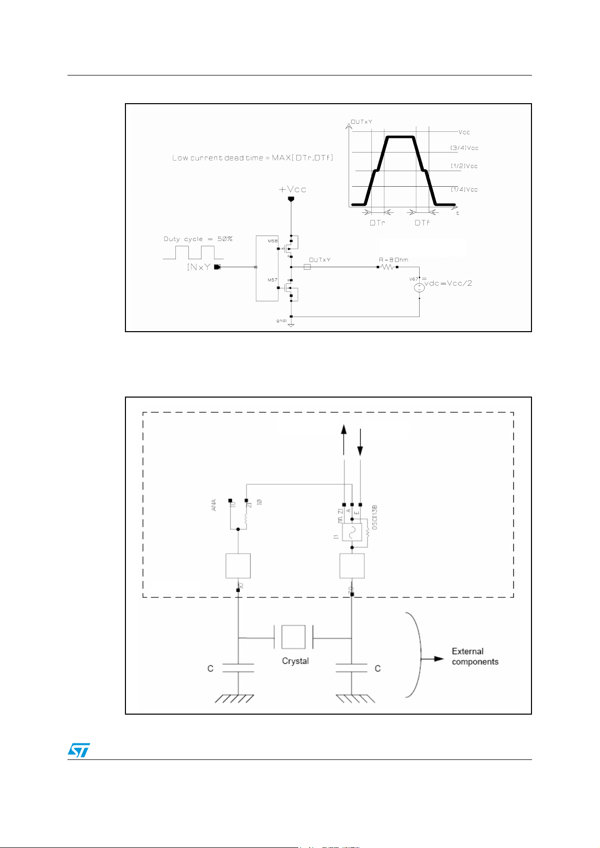
3.4 Embedded crystal oscillator
Figure 4. Oscillator configuration
XTI
STA321
To PLL
Enable from register bit MISC[7]
XTO
Doc ID 15351 Rev 3 17/157
Electrical specifications STA321
The STA321 has an integrated oscillator between pins XTI and XTO.
The architecture is a single-stage oscillator with an inverter working as an amplifier. The
oscillator stage is biased by an internal resistor (of about 500 kΩ), and requires an external
PI network consisting of a crystal and two capacitors as shown in Figure 4 below. An enable
feature is provided in bit 7 of register MISC (address 0xC8) to stop the oscillator and thereby
to reduce power consumption.
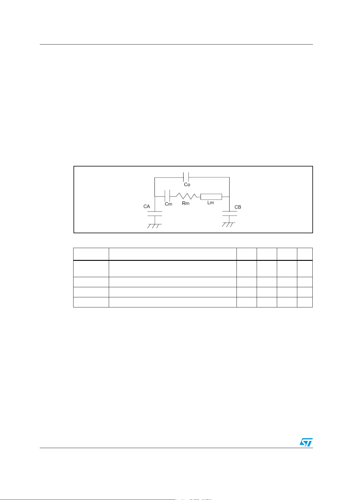
Not all crystals operate satisfactorily with the type of oscillator used in the STA321. To find
out if a crystal is suitable for this device the following transconductance formula must be
evaluated and compared to the critical transconductance for the embedded oscillator:
Gm = Rm * ω
2
* (C + 2 * Co)2 < Gm
CRITICAL
/ 3
where ω is the crystal operating frequency, C = CA = CB, Co and Rm are shown in Figure 5
and Gm
CRITICAL
is given in Table 7 .
Figure 5. Equivalent circuit of crystal and external components
Table 7. Oscillator specifications
Symbol Parameter Min Typ Max Unit
I
OSC
Duty
OSC
T
UP
Gm
CRITICAL
1. If no crystal is connected then the power consumption could be much higher.
2. τx is the time constant of the crystal and external components; a typical value is 44 µs.
Oscillator power consumption with crystal
connected
(1)
--215µA
Duty cycle 46.9 47.8% 48.9 %
Startup time - 15 * τx- s
(2)
Oscillator transconductance 1060 - - µA/V
18/157 Doc ID 15351 Rev 3
STA321 Electrical specifications
3.5 Embedded DC regulator
The power supply to the digital STA321 core and PLL is provided via embedded linear DC
regulators as shown below in Figure 6. When pin REG_BYPASS is tied to ground, the DC
regulators are active so that a voltage in the range 2.5 V to 3.6 V applied to pins VDD_REGx
or PVDD provides a regulated internal voltage to the core and the PLL. The voltages Vddi
and Vddipll range from 1.55 V to 1.95 V depending on operating conditions.
Figure 6. Embedded DC regulator scheme
PVDD
DC
DC
DC
Vddi
Vddi
Vddipll
Core
PLL
STA321
VDD_REG1
VDD_REG2
REG_BYPASS
If the application allows multiple supplies or the power supply requirements are a
fundamental constraint, pin REG_BYPASS can be tied high and a 1.8 V external supply can
be applied directly to pins VDD_REGx and PVDD. In this case the operating range for such
an external supply is 1.55 V to 1.95 V.
Embedded DC regulators imply also static power consumption that must be take into
account when the power-down modes are active. The STA321 provides a deep powerdown
mode where also the regulators are active but in a low power consumption mode (see
Section 4.3.2 on page 27).
Doc ID 15351 Rev 3 19/157
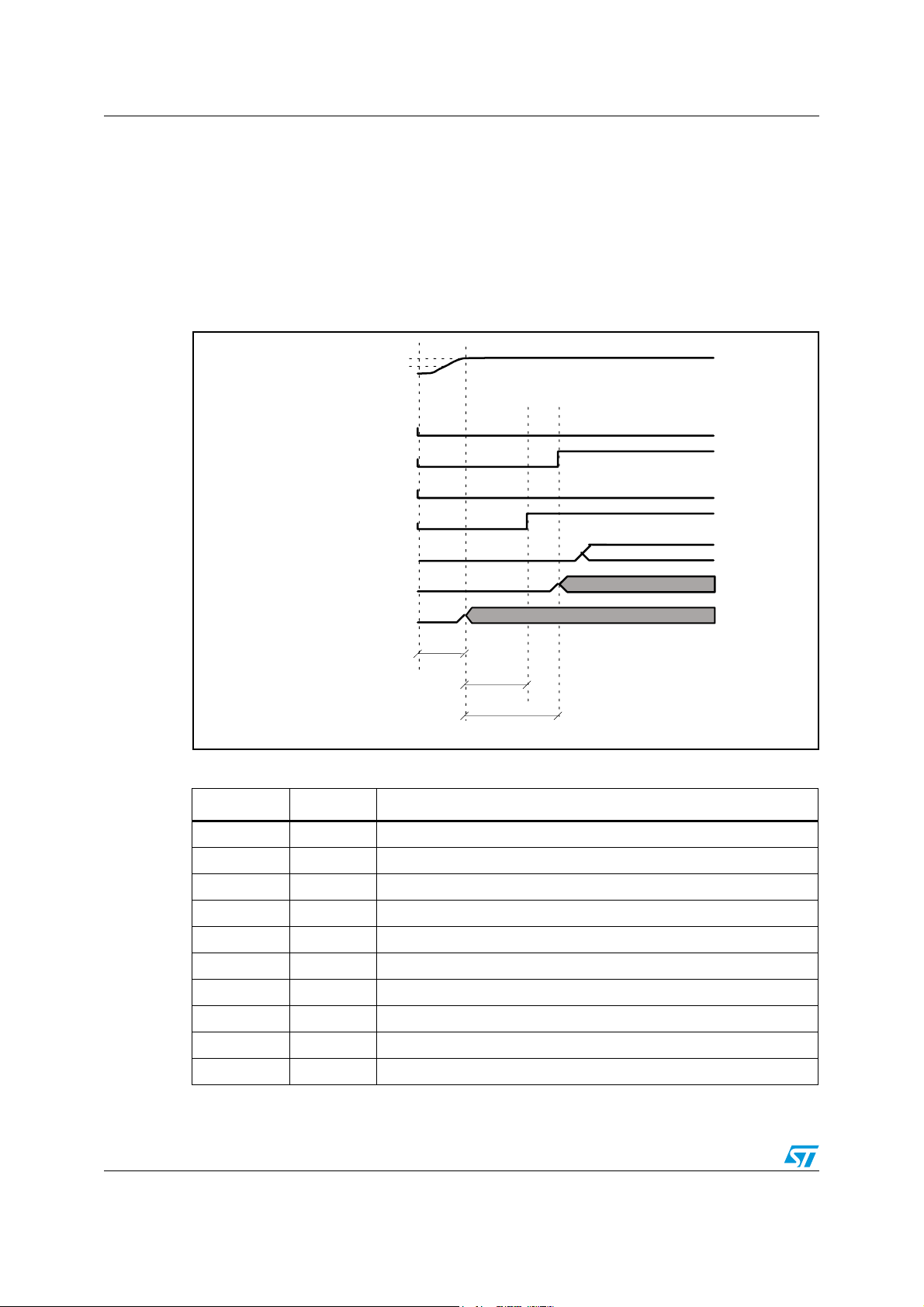
Power-up and power-down sequences STA321
K
4 Power-up and power-down sequences
4.1 Device power-up
After providing the power supply to the device, it is necessary to wait until the DC regulator
PWUP time has elapsed before the device can be set up and used for normal operations.
(see Figure 7).
Figure 7. Startup sequence
VVDDIO
VDDIO
PVDD
3v3
2v2
VDDREG
VVDD_REG
VPVDD
STBY (active H)
STBY (active H)
RSTN (active L)
RSTN (active L)
DC Reg. PWDN
PWDN (active H)
(active High)
DC Reg. A. OK
(active High)
A.OK (active H)
I2C Writings
I2C read
I2C CL
I2C clock
XTI /MCLK
XTI / MCLK
Vdd ramp
DC reg. PWUP time
Table 8. Power-up signal description
Device in reset mode
User configuration via I2C
Signal/pin Type Description
VDDIO Supply Power supply of the digital pads (= VDDIO1,2)
VDD_REG Supply Power supply of the system core (= VDD_REG1,2)
PVDD Supply Power supply of the PLL
STBY In (digital) External standby signal provided by the user
RSTN In (digital) External reset signal provided by the user
PWDN Internal Power-down of the DC regulator cell, controlled by the core
A. OK Internal DC regulator status, when active the 1.8 V is provided to the core
2
C read In (I2C) Configuration commands coming to the I2C interface
I
2
I
C clock Internal I2C peripheral clock
XTI/MCLK In (digital) Clock input source
20/157 Doc ID 15351 Rev 3
STA321 Power-up and power-down sequences
Table 9. Startup timings
Parameter Description Min Typ Max Unit
DC reg. power-up time
Device in reset mode
Table 10. Configuration example
Register
address
Start up time of the DC Regulator after
connecting the power
Must be greater than
(VDD time + DC reg. power-up time)
- - 300 µs
---µs
Value Description
0xC9 0x00 Remove PLL bypass
0xCA 0x00 Headphone detection polarity = 0
0xB8 0x4A Configure SAI output: SAI_out1 = SAI_in1, SAI_out2 = SAI_in2
0xB7 0x38 SRC source select: SRC1 = ADC, SRC2 = ADC
0xC6 0x02 ADC clock on
2
0xB2 0xF3 I
S configuration
0xC8 0x21 Core clock on, SAI/ADC audio set to 32 kHz - 48 kHz range
0xB2 0xD3 SAI_out: output enabled
0xA0 0x00 Soft volume removed
0x00 0x00 Remove bridge 3-state
4.2 Software power-down mode
The software power-down is obtained by configuring the appropriate I2C registers.
In order to obtain flexibility every peripheral has its independent, standby signal and several
gating clock cells are available.
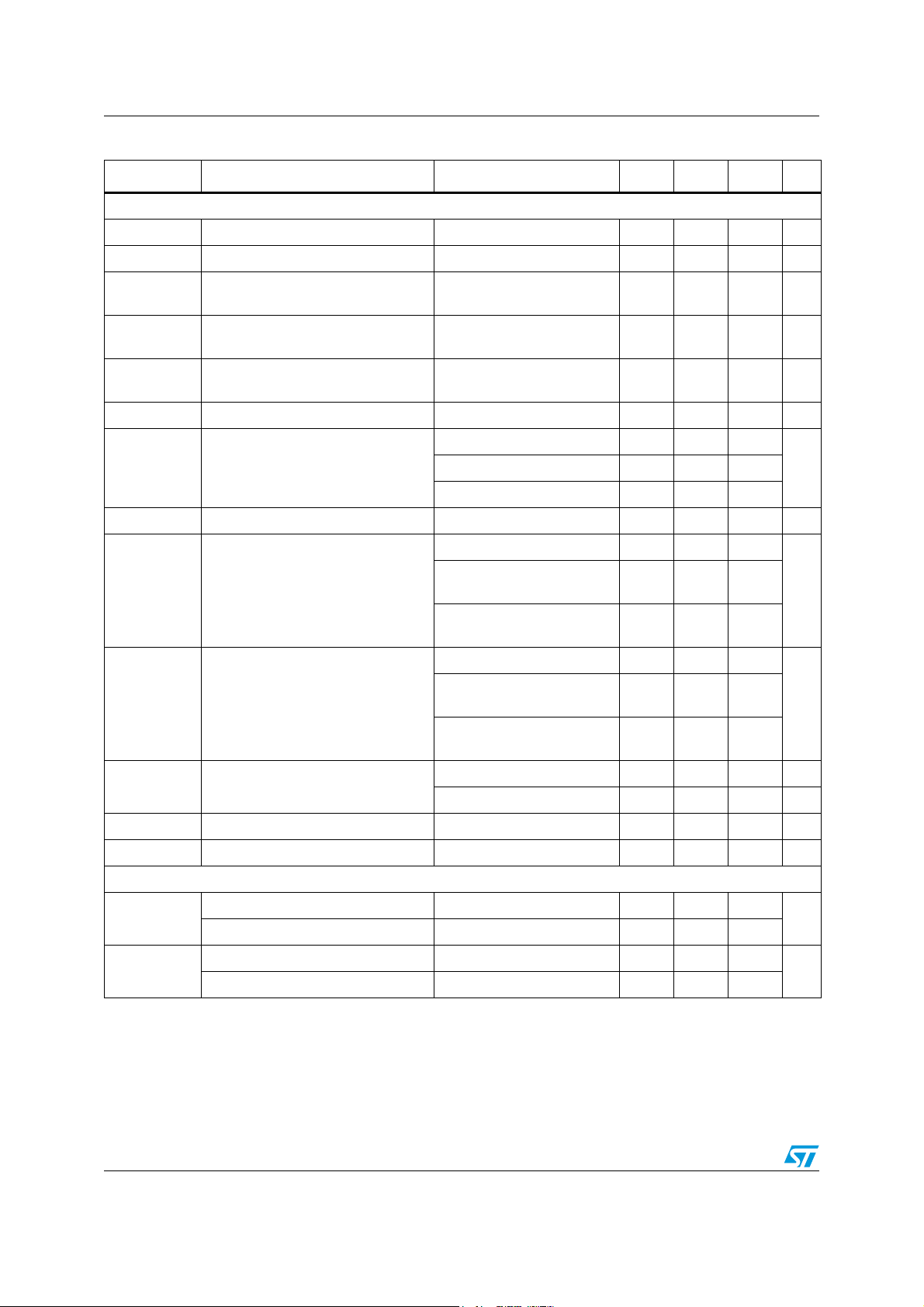
Obviously, the I
recover from the power-down state only via the reset pin.
In the table below EA is embedded amplifier and CB is CMOS bridge. For complete
information this table must be used in conjunction with Chapter 14: Register description on
page 77.
Table 11. Registers for power-down
Put EA in standby FFXCFG1[7] 0x00 on page 81
Put CB in standby FFXCFG1[6] 0x00
Put PLL in standby PLLPFE[5] 0xC4 on page 132
Put ADC in standby ADCCFG0[3] 0xC6 on page 133
Turn core clock off MISC[0] 0xC8 on page 135
Turn ADC clock off ADCCFG0[1] 0xC6
2
C peripheral can not be turned off in this mode, otherwise the device can
Description Register bit Address
Doc ID 15351 Rev 3 21/157
Power-up and power-down sequences STA321
Table 11. Registers for power-down (continued)
Description Register bit Address
Turn SRC clock off CKOCFG[3] 0xC7 on page 134
Turn PROC clock off CKOCFG[2] 0xC7
Turn FFX clock off CKOCFG[4] 0xC7
4.2.1 Configuration example
This is an example of the register setup for power-down clock. It is assumed that every
peripheral is already configured and working correctly.
There are other configuration examples to help you get started please refer to other
chapters and also to Chapter 14: Register description on page 77 in order to get all the
necessary and complementary details.
Turn off all the peripherals.
Note: The MCLK (or XTI) must be used as system clock (sys_clk) before setting the PLL to
standby.
Table 12. Example configurations for power-down
Register bit Address Value Description
EA_STBY
CB_STBY
0x00 on page 81 0xC0
Set the embedded power amplifier and CMOS
bridge to power-down
CLK_FFX_ON 0xC7 on page 134 0x0C Turn off the FFX modulator clock
ADC_STBY 0xC6 on page 133 0x09 Set the ADC into standby mode
CLK_ADC_ON 0xC6 0x80 Turn the ADC clock off
CLK_PROC_ON 0xC7 0x08 Turn the processing clock off
CLK_SRC_ON 0xC7 0x00 Turn the sample rate converter clock to off
Bypass the PLL clock and use MCLK (or XTI) as
PLL_BYP_UNL 0xC4 on page 132 0x80
source clock when the PLL is not locked (a
safety operational mode)
PLL_PWDN 0xC4 0xA0 Put the PLL in standby
CLK_CORE_ON 0xC8 on page 135 0x00 Turning off the core clock
22/157 Doc ID 15351 Rev 3
STA321 Power-up and power-down sequences
_
_
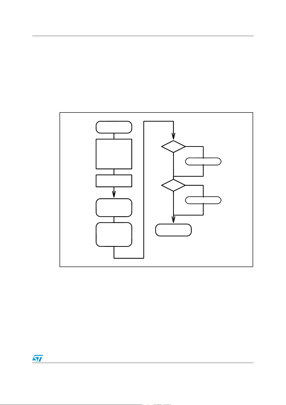
4.3 Hardware power-down mode
The hardware power-down is obtained by asserting pin STBY to high.
There are two power-down options available, namely mild mode and full (or deep) mode,
that could be selected using the DC_STBY_EN signal in register STBY_MODES
Figure 8 summarizes the main power-down sequence. “Power on” is the normal operating
status where all the startup procedures have already been executed. The rectangular boxes
indicate the steps to be done by the user whilst the rounded boxes indicate the steps done
by the device.
Figure 8. Hardware power-done sequence
Power on
2
I
C programming
register
STBY_MODES
bits:
CMP_EN_N
DC_STBY_EN
CMP_EN_N = 1 ?
NO
YES
Comp Cell Pwdn
Pin STBY <= 1'
DC_STBY_EN = 1 ?
NO
YES
DC Reg. Stby
Embedded amp.
CMOS bridge
Powerdown
I2C off
CLK
CLK
ADC off
Power-down mode
CLK Core off
PLL power down
Doc ID 15351 Rev 3 23/157
Power-up and power-down sequences STA321
Table 13. Frequently used signals
Name Description
STBY Input pin STBY on page 11
PWDN
DC regulator
Internal
A. OK
DC regulator
Internal
CMP_EN_N Bit 1, register STBY_MODES on page 139
EA_STBY
CB_STBY
Bits 7:6, register FFXCFG1 on page 81
EA/CB volume Internal
PLL_UNLOCK Bit 7, register PLLST on page 132
PLL_PWDN Bit 5, register PLLPFE on page 132
CLK_PROC_ON Bit 2, register CKOCFG on page 134
CLK_PROC Processing clock
CLK_FFX_ON Bit 4, register CKOCFG on page 134
clk_ffx FFX clock
CLK_ADC_ON Bit 1, register ADCCFG0 on page 133
clk_adc ADC clock
CLK_SRC_ON Bit 3, register CKOCFG on page 134
clk_src SRC clock
CMP_EN_N Bit 1, register STBY_MODES on page 139
DC_STBY_EN Bit 0, register STBY_MODES on page 139
FFX_ULCK_PLL Bits 4:3, register FFXCFG1 on page 81
24/157 Doc ID 15351 Rev 3

STA321 Power-up and power-down sequences
4.3.1 Mild power-down
In this case, the device is put into a mild power-down mode.
All the peripherals are set to standby and their clocks turned off.
2
The I
C configuration is not required as the default values of the registers are sufficient.
z Initial conditions:
FFX_ULCK_PLL = 10
CMP_EN_N = 0
DC_STBY_EN = 0
z Going into power-down:
After the assertion of the pin STBY, the following actions are taken by the device:
1. Embedded amplifier (EA) and CMOS bridge (CB) volume are set to mute (the length of
this step changes according to the fade-out ramp configuration).
2. EA and CB are put into power-down.
After the previous operation is completed:
3. All peripherals are turned off (regardless the register settings).
4. The PLL clock is bypassed, the system clock (sys_clk in Figure 11 on page 29) is XTI.
5. All clocks are shut down.
z Returning to normal mode:
After the release of the pin STBY, the power-up procedure takes place:
1. All clocks are turned on.
2. All peripherals are restored to their previous status (based on the last register settings).
3. If the PLL clock was the system clock it will be selected again after the locking time.
4. The EA and the CB execute the fade-in procedure before becoming ready to be used
(the length of this step changes according to the fade-in ramp configuration).
Doc ID 15351 Rev 3 25/157
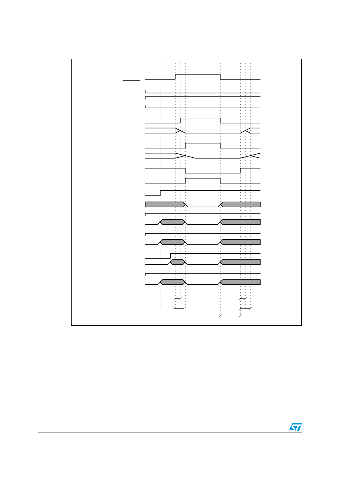
Power-up and power-down sequences STA321
Figure 9. Hardware powerdown sequence (mild mode)
STBY (active H)
DC Reg. PWDN
(active High)
DC Reg. A. OK
(active High)
Comp Cell PWDN
(active High)
EA is in Pwdn
EA Volume
CB is in Pwdn
CB Volume
PLL LOCKED
(active High)
PLL_PWDN
(active High)
I2C [CORE_CLK_ON]
CLK_I2C
Operational Volume
Operational Volume
MUTE O.V.
O.V.MUTE
I2C [CLK_PROC_ON]
CLK_PROC_CLK
I2C [CLK_FFX_ON]
CLK_FFX_CLK
I2C [CLK_ADC_ON]
CLK_ADC_CLK
I2C [CLK_SRC_ON]
CLK_SRC_CLK
E.A Fade InE.A Fade Out
Bridge Fade Out Bridge Fade In
PLL Locking Time
26/157 Doc ID 15351 Rev 3

STA321 Power-up and power-down sequences
4.3.2 Full power-down
In this case the device is put into a full power-down mode.
This implies lower power consumption than the mild mode, but has a drawback in that it
takes longer to execute.
z Initial conditions
FFX_ULCK_PLL = 10
CMP_EN_N = 1
DC_STBY_EN = 1
z Going into power-down:
This mode differs from the previous one by an additional step at the end of the powerdown procedure and at the beginning of the power-up:
1. Embedded amplifier (EA) and CMOS bridge (CB) volume are set to mute (the length of
this step changes according to the fade-out ramp configuration).
2. EA and CB are put into power-down.
After the acknowledge signals (EA is in power-down and CB is in power-down) are
received:
3. All peripherals are turned off (regardless the register settings).
4. PLL clock is bypassed, the system clock (sys_clk in Figure 11 on page 29) is XTI.
5. All clocks are shut down.
6. DC regulator is put into standby mode. After this point the device is in a very low power
consumption mode.
z Returning to normal mode:
After the release of pin STBY, the power-up procedure will take place:
1. DC regulator is set to operational mode
After the acknowledge signal (DCAOK) from the DC regulator is received:
2. All clocks are turned on.
3. All peripherals are restored to the status based on their relative register settings.
4. If the PLL clock was the system clock it is selected again after the locking time.
5. The EA and the CB execute the fade-in procedure before being ready to be used (the
length of this step changes according to the fade-in ramp configuration).
Doc ID 15351 Rev 3 27/157
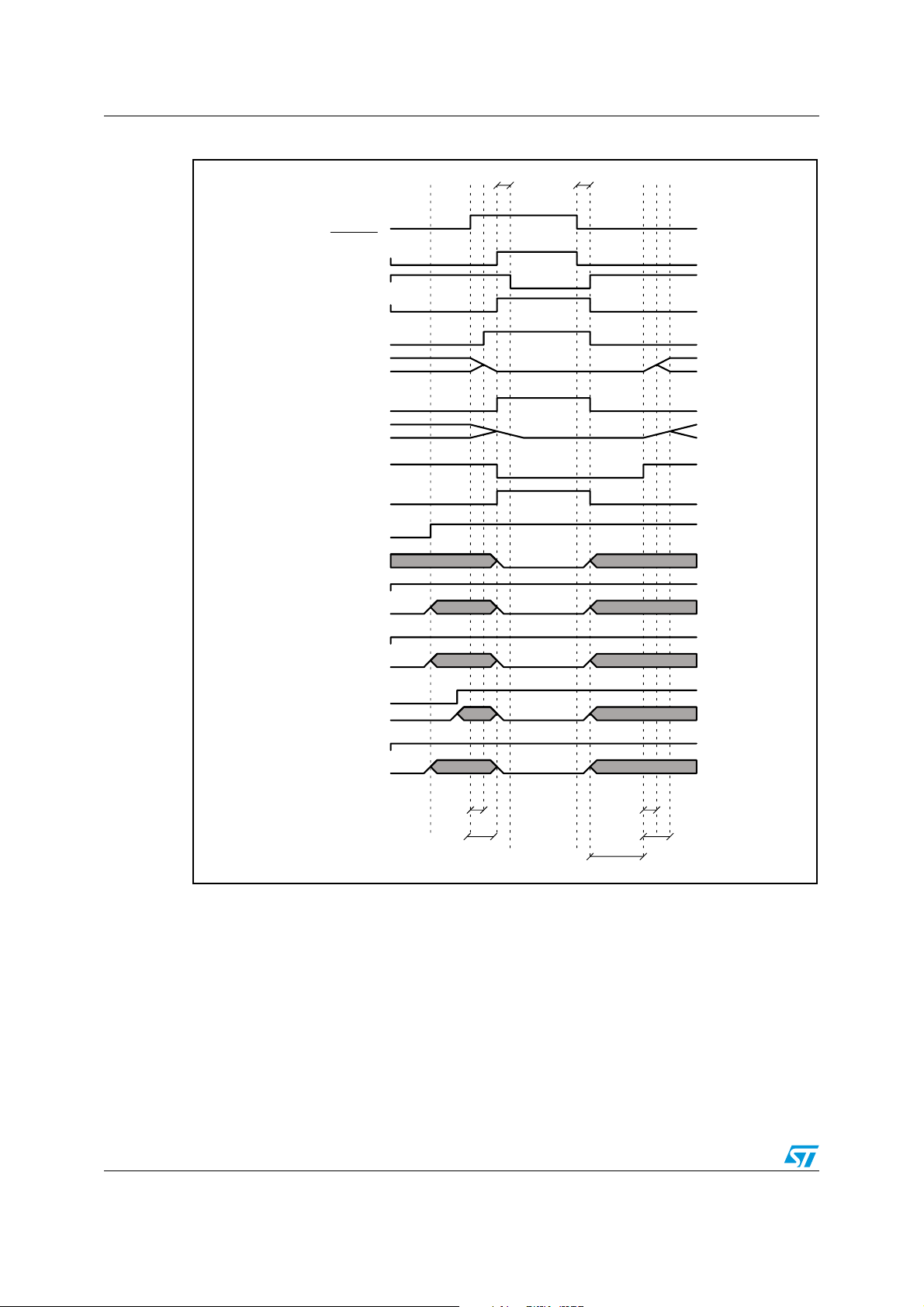
Power-up and power-down sequences STA321
DC- Td
Figure 10. Hardware power-down sequence (full mode)
STBY (active H)
DC Reg. PWDN
(active High)
DC Reg. A. OK
(active High)
Comp Cell PWDN
(active High)
EA is in Pwdn
EA Volume
CB is in Pwdn
CB Volume
PLL LOCKED
(active High)
PLL_PWDN
(active High)
I2C [CORE_CLK_ON]
CLK_I2C
own
Operational Volume
Operational Volume
DC- Tup
MUTE O.V.
O.V.MUTE
I2C [CLK_ PROC_ON]
CLK_PROC_CLK
I2C [CLK_FFX_ON]
CLK_FFX_CLK
I2C [CLK_ADC_ON]
CLK_AD C_CLK
I2C [CLK_SRC_ON]
CLK_SRC_CLK
E.A Fade InE.A Fade Out
Bridge Fade Ou t Bridge Fade In
PLL Locking Time
28/157 Doc ID 15351 Rev 3
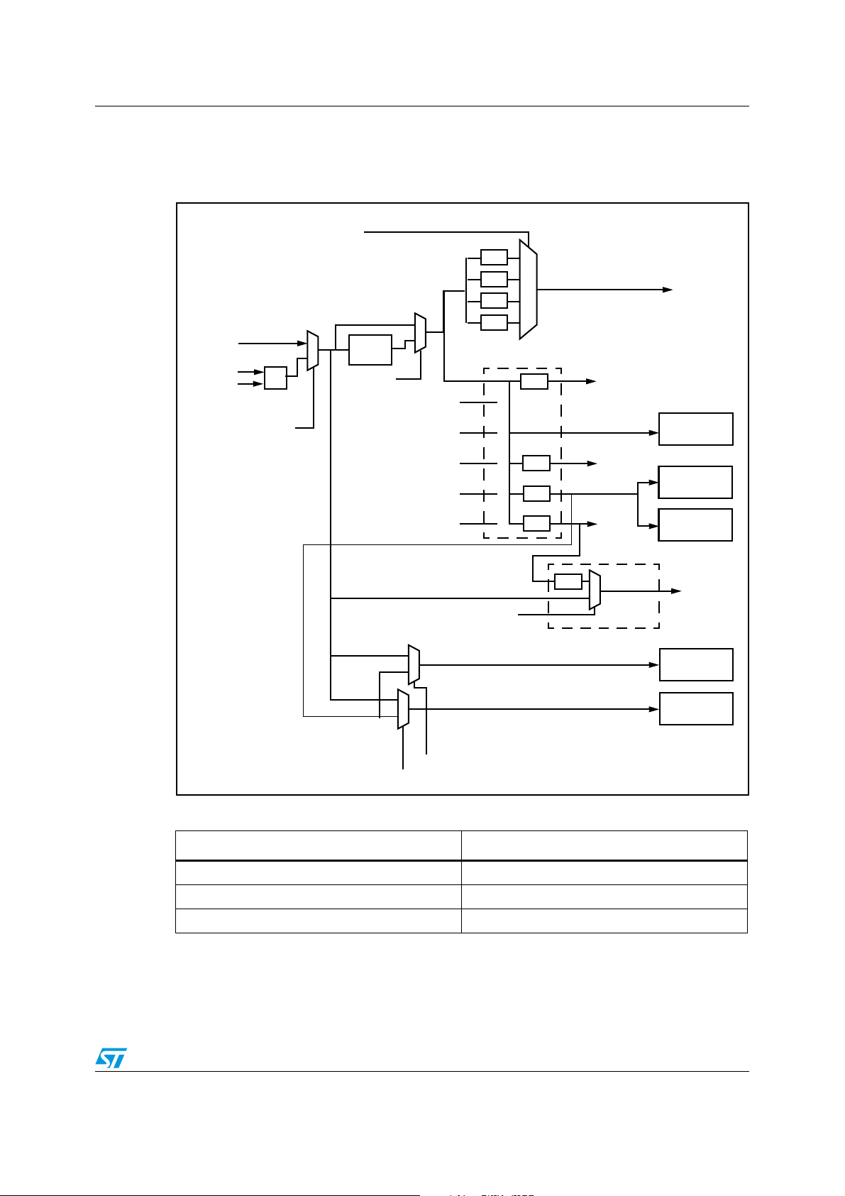
STA321 Clock management
5 Clock management
Figure 11. Clock management scheme
CKOCFG[6:5]
CLKOUT_SEL
11
1/2
1/8
1/8
1/4
10
00
01
1/2
1/2
1/2
1/2
clk_i2c
clk_ffx
clk_src
clk_proc
clk_adc
CLKOUT
FFX
SAI_in1
SAI_in2
BICLKI1
MCLK
XTI
OR
PLLPFE[6]
BICLK2PLL
pll_clk_in_i
1
0
PLL
PLLB[7]
CLK_CORE_ON
CKOCFG[4]
CLK_FFX_ON
CKOCFG[3]
CLK_SRC_ON
CKOCFG[2]
CLK_PROC_ON
ADCCFG[1]
CLK_ADC_ON
sys_clk
1
0
Clock management
MISC[0]
ADC
1/4
0
clk_adc_in
1
PLLB[5] ADC_CLKSEL
clk_proc
1
0
1
0
SAI_out1
SAI_out2
PLLB[3] P2S1_CLKSEL
PLLB[1] P2S2_CLKSEL
Table 14. Clock control registers
Register Name Address
PLLB on page 136 0xC9
ADCCFG0 on page 133 0xC6
CKOCFG on page 134 0xC7
Doc ID 15351 Rev 3 29/157
Clock management STA321
Table 15. Clock characteristics
Symbol Parameter Min Typ Max Unit
f
MCLK_Range
Duty
MCLK
t
MCLK_RF
f
XTI_Range
Duty
XTI
t
XTI_RF
f
BICLK1_Range
Duty
BICLK1
t
BICLK1_RF
f
CLKOUT_Range
Input clock frequency range 2.048 - 49.152 MHz
Input clock duty cycle 40 - 60 %
Input clock rise/fall time - - 0.2 ns
Input clock frequency range 2.048 - 49.152 MHz
Input clock duty cycle 40 - 60 %
Input clock rise/fall time - - 0.2 ns
Input clock frequency range 2.048 - 49.152 MHz
Input clock duty cycle 40 - 60 %
Input clock rise/fall time - - 0.2 ns
Output clock frequency range - - 49.152 MHz
5.1 System clock
Figure 11 above shows the STA321 clock management scheme with all the major clocks. As
can be seen, the system clock (sys_clk) is selected from one of three sources by using
register PLLB on page 136:
z an external clock BICLKI1
z (default) an external clock XTI or MCLK (the unused one must, however, be set to 0)
z the internal PLL.
If the PLL is used there are some design constraints:
z pll_clk_in_i must be in the range: 2.048 MHz to 49.152 MHz
z pll_clk_out must be in the range: 65.536 MHz to 98.304 MHz.
The sys_clk is routed to the peripherals through the clock manager section.
5.1.1 Configuration example
This is an example of the PLL register setup. It is assumed that every peripheral is already
configured and working correctly.
There are other configuration examples to help you get started please refer to other
chapters and also to Chapter 14: Register description on page 77 in order to get all the
necessary and complementary details.
Starting with MCLK as system clock switching to PLL as source
Table 16. Register setup to provide sys_clk from MCLK to PLL
Register Address Value Description
PLLPFE 0xC4 0x80
PLLB 0xC9 0x00 Remove the PLL bypass and use its clock as system
Safety operational mode: automatic use of MCLK (or XTI)
as system clock if the PLL is not locked
30/157 Doc ID 15351 Rev 3

STA321 Clock management
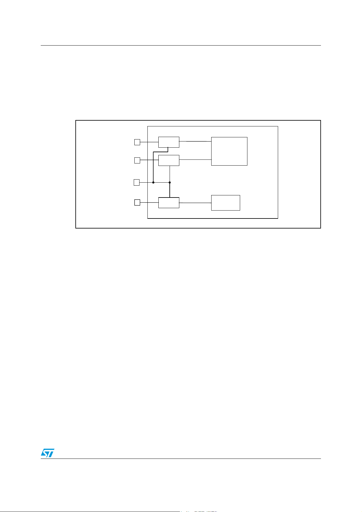
r
5.2 Peripheral clock manager
This block manages the clocks of the core processing peripherals ADC, FFX, PROC
(including memories and SAI interfaces) and SRC.
A clock divider (by 2) is attached before every block except the FFX.
Each block is attached to a global gating cell and to a dedicated one. This allows a flexible
power-consumption management because it is possible to turn off either the whole
processing chain or just a single block. The only exception is the I
2
C peripheral clock which
is disabled only when the device is in hardware power-down mode. In all the other cases this
clock remains active.
5.3 Fractional PLL
The PLL specifications are given in Table 6 on page 14.
Figure 12. PLL block diagram
PLL_CLK_in
pll_clk_in
PLLCFG0(3-0)
PLLCFG0[3:0]
CLKIN
CLKIN
IDF
IDF
IDF
Input freq. divider
Lock detect
F_INT
LOCKP
LOCKP
PLLCFG3(7)
PLLCFG3[7]
PLLCFG3[6]
PLLCFG3(6)
PLLCFG0[6]
PLL_FR_CTRL
PLLCFG0(6)
5.3.1 PLL block description
Phase/frequency detector (PFD)
This block compares the phase difference between the corresponding rising edges of the
F_INT and the clock coming from the loop frequency divider.
It generates voltage pulses with widths proportional to the input phase error.
Charge pump and loop filter (LPF/CPUMP)
PLL_PWDN
PLL_PWDN
pll_strb
PLL_STRB
pll_strbbyp
PLL_STRBBYP
pll_fr_ctrl
Buffer
DITHER
DITHER
Disable
PLLCFG0(5-4) PLLCFG1(7-0)
Disable
PLLCFG0[5:4]
PFD
LDF
Loop freq. divider
Fractional
controlle
FRAC
FRAC
Input
Input
PLLCFG2(7-0)
PLLCFG1[7:0]
PLLCFG2[7:0]
LPF
cpump
NDIV
NDIV
PLLCFG3(5-0)
PLLCFG3[5:0]
VCO
FVCO
FVCO
This block converts the voltage pulses from the phase/frequency detector to current pulses
which charge the loop filter and generate the control voltage for the voltage controlled
oscillator (VCO).
Doc ID 15351 Rev 3 31/157

Clock management STA321
Voltage controlled oscillator (VCO)
This is the oscillator inside the PLL, which produces a frequency, f
proportional to the input control voltage.
Input frequency divider (IDF)
This frequency divider divides the PLL input clock CLKIN by the input division factor (IDF) to
generate the PFD input frequency. IDF is programmed in register PLLCFG0[3:0].
Loop frequency divider (LDF)
This frequency divider is present within the PLL for dividing the VCO output by the loop
division factor (LDF). LDF is programmed in register bits PLLCFG3[5:0].
Lock circuit
The output of this block, signal LOCKP, is asserted high when the PLL enters the state of
coarse lock in which the output frequency is ±10% of the desired frequency. LOCKP is
refreshed every 32 cycles of F_INT. The status bit PLL_UNLOCK is in register PLLST on
page 132.
5.3.2 Output frequency computation
The input clock frequency of the phase/frequency detector (PFD) is
f
= CLKIN / IDF
F_INT
The VCO frequency depends on the value of register bit PLLCFG0.PLL_FR_CTRL such
that
, on output FVCO
VCO
When PLL_FR_CTRL = 1
f
VCO
= f
* (LDF + FRAC / 216 + 1 / 217)
F_INT
and when PLL_FR_CTRL = 0
f
VCO
= f
F_INT
* LDF
Notes:
1. When dither is disabled (PLL_DDIS = 1), the factor 1 / 2
17
is not used in the multiplication.
2. There are some limits to the input and output frequencies as given in Ta bl e 1 7 and
Ta bl e 1 8 when selecting the values for IDF, LDF, and FRAC.
3. The LDF values of 5, 6 and 7 cannot be used when fractional synthesis mode is on, that
is, when PLL_FR_CTRL = 1.
4. The fractional control bits (FRAC_INPUT) must be set to the required values before
activating the fractional synthesis mode.
Table 17. Input division factor (IDF)
IDF[3] IDF[2] IDF[1] IDF[0] Input division factor (IDF)
00001
00011
00102
……………
32/157 Doc ID 15351 Rev 3

STA321 Clock management
Table 17. Input division factor (IDF) (continued)
IDF[3] IDF[2] IDF[1] IDF[0] Input division factor (IDF)
111014
111115
Table 18. Loop division factor (LDF)
NDIV[5] NDIV[4] NDIV[3] NDIV[2] NDIV[1] NDIV[0] Loop division factor (LDF)
0000xxNA
000100NA
0001015
0001106 (see note 3)
0001117 (see note 3)
0010008
…………………
11011054
11011155
(1)
111xxxNA
1. The LDF values of 5, 6 and 7 cannot be used when fractional synthesis mode is ON (PLL_FR_CTRL = 1)
Doc ID 15351 Rev 3 33/157

Digital processing stage STA321
r
r
6 Digital processing stage
6.1 Signal processing flow
The STA321 provides 4 channels of audio signal processing. The block diagram is shown in
the following figure.
Figure 13. Processing flow
-1
kZ
kZ
kZ
kZ
Delay
Vol 0
-1
-1
-1
Post mix
Vol 1
Vol 2
Volume control
Master volume
Limite
FFX modulator
Processing data mux
Sample
rate
converte
- G0
- G1
Pre mix
- G2
- G3 Vol 3
Pre scaler
Bq0
Bq0
Bq0
Bq0
EQ - tone control
Bq12
Bq12
Bq12
Bq12
13 biquads
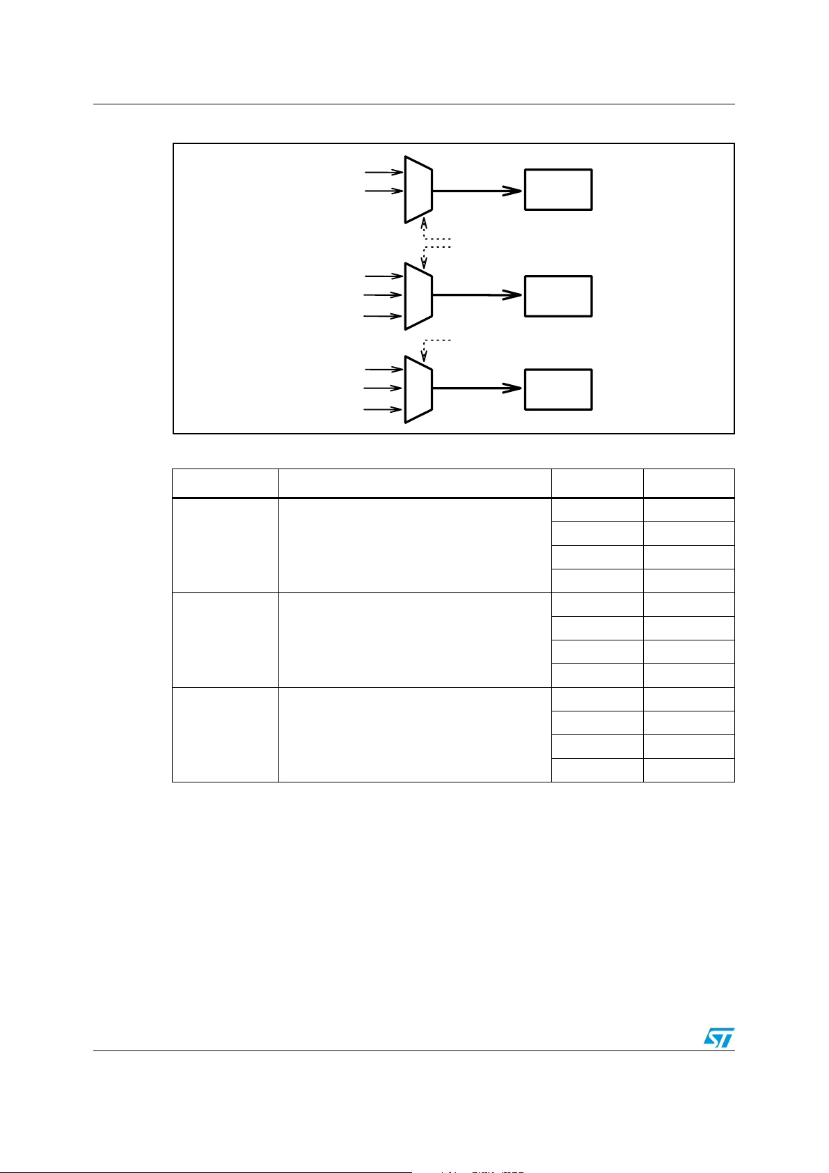
Left and right channels coming from the two serial audio interfaces and ADC (left and right
channels) are fed into the selection multiplexer (controlled by register SRCINSEL on
page 128), so that each channel can be connected to any desired processing chain. The
four channels are then sample rate converted to the fixed internal sampling rate. Pre mix,
EQ/tone processing, programmable delay, post mix, and volume/limiter make up the
STA321 signal processing chain.
Figure 14. Processing data multiplexer
SRCINSEL[7:6]
24
24
24
24
20
20
20
20
2-channel signal
1-channel signal
To SAI_ o u t
multiplexers
FFX
SAI_in1
ADC
SAI_in2
32
00
16
01
32
10
SRC1
24
ch0_in
ch1_in
PROC ch0
PROC ch1
PROC ch2
PROC ch3
Processing
SAI_in1
ADC
SAI_in2
32
00
16
01
32
10
SRC2
24
ch2_in
ch3_in
ch0_out
ch1_out
ch2_out
ch3_out
SRCINSEL[5:4]
34/157 Doc ID 15351 Rev 3

STA321 Digital processing stage
Figure 15. SAI_out data multiplexer
P2SDATA[5:3]
ADC (L/R)
SAI_in1 (L/R)
SAI_in2 (L/R)
SRC1 (L/R)
SRC2 (L/R)
PROC (ch0/ch1)
PROC (ch2/ch3)
ADC (L/R)
SAI_in1 (L/R)
SAI_in2 (L/R)
SRC1 (L/R)
SRC2 (L/R)
PROC (ch0/ch1)
PROC (ch2/ch3)
6.2 Sampling rate converter
The sample rate converter (SRC) re samples the input data source in order to send to the
processing block an audio stream always with a fixed frequency:
sampling frequency, f
In all the examples given here, f
S
= f
sys_clk
= 96 kHz.
S
16
000
32
001
32
010
24
011
24
100
24
101
24
else
16
000
32
001
32
010
24
011
24
100
24
101
24
else
P2SDATA[2:0]
/ 1024 where f
SAI_out1
2-channel signal
1-channel signal
SAI_out2
is the system clock frequency.
sys_clk
Figure 16. Sample rate converter block diagram
Data input
LRCK_IN
Interpolation
FIR x2
DRLL
Threshold
selector
Ratio
Interpolation
FIR x2
Precomp.
FIR
Sync 6
async.
Data output
The selection between x2 FIR interpolation and direct input data is made automatically by
the threshold selector block. If the input sampling frequency (measured by the DRLL) is
higher than the SRC threshold (that is, more than 81 kHz) the direct connection is selected
(first filter bypassed), otherwise the first x2 filter is added to the data path.
A 3-kHz hysteresis is fixed around the SRC threshold nominal value in order to prevent
unstable oscillations.
Doc ID 15351 Rev 3 35/157

Digital processing stage STA321
6.3 Pre-EQ mix 1 and post-EQ mix
The four-channel data, received from the sample rate converters, is sent to Mix1 block to
produce the four mixed-channel data for processing. All this data can be mapped to any
internal processing channel through the appropriate configuration of the RAM memory
locations.
Table 19. Channel mapping
Function Channel Memory location (RAM)
Ch0 from 0x00
Pre mixer
Post mixer
Ch1 from 0x04
Ch2 from 0x08
Ch3 from 0x0c
Ch0 from 0x118
Ch1 from 0x11c
Ch2 from 0x120
Ch3 from 0x124
The post-EQ mixer acts in a similar way for the output channels from the processing and
directed to the FFX. It is placed after the delay block which provides a full 4-channel input
mix on every channel.
Figure 17. Mixers block diagram
G2_0
pre: 0x08
pos: 0x120
ch0_in
pre: 0x00
pos: 0x118
G0_0
ch0_in
ch1_in
ch2_in
G0_1
G0_2
pre: 0x01
pos: 0x119
pre: 0x02
pos: 0x11A
ch0_out
++
ch1_in
ch2_in
G2_1
G2_2
pre: 0x09
pos: 0x121
pre: 0x0A
pos: 0x122
ch2_out
ch3_in
G0_3
pre: 0x03
pos: 0x11B
ch3_in
G2_3
pre: 0x0B
pos: 0x123
pre: 0x04
ch0_in
G1_0
pos: 0x11C
pre: 0x05
ch1_in
G1_1
pos: 0x11D
pre: 0x06
ch2_in
ch3_in
pos: 0x11E
G1_2
pos: 0x11Ff
G1_3
pre: 0x07
ch1_out
+
ch0_in
ch1_in
ch2_in
ch3_in
G3_0
G3_1
G3_2
G3_3
pre: 0x0C
pos: 0x124
pre: 0x0D
pos: 0x125
pre: 0x0E
pos: 0x126
pre: 0x0F
pos: 0x127
ch3_out
+
36/157 Doc ID 15351 Rev 3
STA321 Digital processing stage
6.3.1 Presets
By default, each mixer output is connected to its corresponding input without any attenuation
and without any mixing with the other channels:
ch0_out = ch0_in, ch1_out = ch1_in, ch2_out = ch2_in, ch3_out = ch3_in.
6.4 Pre scaler
The pre scale block, which precedes the first biquad, could be used to attenuate the input
signal when the filters of the processing chain have a gain that could reach the clamping
value.
Each channel has a dedicated 24-bit signed multiplier in the range -1 (0x800000) to almost
+1 (0x7FFFFF).
6.4.1 Presets
By default, all pre-scale factors are set to 0x7FFFFF
6.5 Equalization, tone control and effects
Figure 18. EQ/tone block diagram
From
prescaler
Biquad
00
Biquad
ReservedRAM
07
ReservedReserved
ReservedRAM
Biquad
08
RAM
To
delay stage
Biquad
09
effects_en[0]
High
pass
treb_sel bass_sel
effects_en[1]
RAM Deemph.
Treble
RAM
Biquad
12
Biquad
10
Reserved
RAM
Reserved
RAM Bass
Biquad
11
Four channels of input data are fed to the EQ processing block which provides 13
user-programmable biquad filters per channel as shown in Figure 18 above.
A description of the biquad programming is given in Section 6.14 on page 44.
Some filter coefficients are pre-programmed and stored in the non-volatile memory in order
to supply particular EQ effects (see Figure 19 and Table 20 on page 38).
The selection of RAM, ROM bass/treble or ROM effects is made using registers
EFFS_EN_CHn on page 109 for the effects and BASS_SELn_R on page 111 and
TREB_SELn_R on page 113 for the bass/treble. Each biquad can be configured
independently.
Doc ID 15351 Rev 3 37/157
Digital processing stage STA321
Figure 19. Biquad coefficient selection
RAM
ROM - Effects
RAM
ROM - Effects
ROM - Bass
RAM
ROM - Effects
ROM - Trebl.
Coefficients
ROMCHxx_
ROMCHxx & BASS_SELxx
Coefficients
ROMCHxx & TREB_SELxx
Coefficients
Biquads (00-10)
Biquads (11)
Biquads (12)
Table 20. EQ control signals
Signal name Description Channel Register addr
Ch0 0x71
Ch1 0x73
effects_en[1] 1: enable deemphasysa filter
Ch2 0x73
Ch3 0x77
Ch0 0x78
Ch1 0X79
bass_sel[5] 1: enable bass tone control
Ch2 0X7A
Ch3 0X7B
Ch0 0X7C
Ch1 0X7D
treb_sel[5] 1: enable treble tone control
Ch2 0X7E
Ch3 0X7F
38/157 Doc ID 15351 Rev 3

STA321 Digital processing stage
6.6 Biquads
The biquads are based on the following equation and is shown diagramatically in Figure 20.
Y[n] = b0 * X[n] + b1 * X[n-1] + b2 * X[n-2] - a1 * Y[n-1] - a2 * Y[n-2]
where Y[n] represents the output and X[n] represents the input. Fractional multipliers
are 24-bit signed with coefficient values in the range -1 (0xFFFFFF) to +1 (0x7FFFFF).
Figure 20. Biquad filter
-1
-1
6.6.1 Presets
By default all the biquads values in RAM are set to give a bypass function; in actual fact, the
signal passes through unchanged. The coefficients for this are:
a1 / 2 = 0, a2 / 2 = 0, b0 / 2 = 0.5 (0x400000), b1 / 2 = 0, b2 / 2 = 0.
6.7 High-pass filter
The standard high-pass filter is provided by the STA321
Figure 21. High-pass filter frequency response
b0/2
b1/2
b2 Z
2
2Z
+
+
+
2
-a1/2
-a2
-1
Z
-1
Z
High Pass Filter
0
−5
−10
−15
Gain [dB]
−20
−25
−30
0
10
1
10
10
2
Freq. [Hz]
3
10
4
10
5
10
Doc ID 15351 Rev 3 39/157

Digital processing stage STA321
6.8 Deemphasis filter
The standard deemphasis filter is provided by the STA321.
Figure 22. Deemphasis filter frequency response
40/157 Doc ID 15351 Rev 3

STA321 Digital processing stage
6.9 Bass and treble control
Preset values for the 11th and 12th biquads of every channel are stored in ROM in order to
achieve a bass and treble tone control.
They are channel independent and have 24 curves ranging from -12 to +12 dB gain with
1 dB steps. Their selection (and enable) is via registers BASS_SELx_R and TREB_SELx_R
where x is the number of the channel to be equalized.
The EQ curve and filter cut-off frequencies are shown in Figure 23 and Figure 24.
With a sampling frequency of 96 kHz (inside the processing block), the cut-off frequencies
are 3 kHz for treble curves and 150 Hz for bass curves.
Figure 23. Frequency responses of treble control at 1-dB gain steps
Figure 24. Frequency responses of bass control at 1-dB gain steps
Doc ID 15351 Rev 3 41/157

Digital processing stage STA321
6.9.1 Configuration example
This is an example of the tone control register setup. It is assumed that every peripheral is
already configured and working correctly.
Ta bl e 2 1 gives the register values to obtain +12 dB of bass on all channels and -10 dB of
treble on channels 0 and 1.
Table 21. Selecting EQ curves
Register - Address Programmed value Description
BASS_SEL0_R 0x38 CH0 +12 dB bass
BASS_SEL1_R 0x38 CH1 +12 dB bass
BASS_SEL2_R 0x38 CH2 +12 dB bass
BASS_SEL3_R 0x38 CH3 +12 dB bass
TREB_SEL0_R 0x22 CH0 -10 dB treble
TREB_SEL1_R 0xx22 CH1 - 10 dB treble
6.10 Programmable delay
Every channel, just after the biquads stage, is connected to a dedicated delay block.
The length of the delay is stored in RAM at location 0x128 and can vary from 0 to 35
samples. The corresponding time delay depends on the processing sampling frequency.
6.10.1 Presets
The delay of every channel is set to 0.
6.11 Volume and mute control
The STA321 provides a flexible volume and mute control stage. Using the registers VOLCH0
to VOLCH3 on page 122 it is possible to set the volume for each channel individually from
+36 dB to -105 dB with 0.5-dB steps.
There is a master volume control, register MVOL on page 120, as well. The master volume
adds an offset to all the individual volume settings.
The mute function offers the possibility to turn off the sound by reducing the volume setting
to -127.5 dB. It could be activated in two ways:
z register FFXCFG0 on page 82 provides a dedicated mute control for each channel.
z pin MUTE, driven by an external signal, puts all four channels into mute mode.
Register VOLCFG on page 120 provides some flexibility to set how the mute and volume
change procedures are applied. If bit SVOL_ONx is activated the volume of channel x is
changed gradually (soft volume or soft mute); using a ramp it starts from the current value
and goes down to the target value or to -127.5 dB for mute. The slope of the ramp is set with
with the value TIM_SVOL which represents how many samples are needed to achieve a
0.5-dB step.
= 2
TIM_SVOL
/ f
t
STEP
S
42/157 Doc ID 15351 Rev 3

STA321 Digital processing stage
The ramp procedure ends when the target volume or mute level is reached. The time for the
volume change is calculated as:
t
CHANGE
= (volume
CURRENT
- volume
TA R GE T
) / 0.5 * t
STEP
If SVOL_ONx is not used, the volume and mute are set instantaneously.
The STA321 also has the possibility to put the FFX into mute in the event of bad input data
using register FFXCFG0. If bit BAD_CKS_M is set to 1 the FFX is muted when BICLK and
LRCLK do not meet the specifications. If MIS_BICK_M is set to 1 the FFX is muted when
BICLK is missing. The mute can be applied gradually or abruptly via bit BAD_IN_M.
6.12 Limiter (clamping)
The saturation stage provides an individual or a global limitation on the output signal
amplitude such that if the signal is above the limiting value then it is truncated (clamped).
A 23-bit saturation value made up using registers SATCHxCFG1, SATCHxCFG2 and
SATCHxCFG3 can be set for each channel x.
However, if bit 7 of register SATCH0CFG1 on page 116 is set to 1, all the channels take the
saturation value of channel 0 and ignore the individual settings.
6.13 FFX channel re-mapping
Figure 25. FFX re-mapping
Processing block
Channle 0
Channel 1
Channel 2
Channel 3
The channels are re-mapped through registers PWMMAP1, PWMMAP2 and PWMMAP3 on
page 86. The default configuration routes the channels directly to their respective CB/EA
signals:
pwm_1a -> cb_pwm_1
pwm_1b -> cb_pwm_2
pwm_2a -> cb_pwm_3
pwm_2b -> pwm_00 (PWM00)
pwm_3a -> ea_pwm_1 (EAPWM1)
pwm_3b -> ea_pwm_2 (EAPWM2)
pwm_4a -> ea_pwm_3 (EAPWM3)
pwm_4b -> ea_pwm_4 (EAPWM4)
FFX block Channel re-map
FFX ch1
FFX ch2
FFX ch3
FFX ch4
pwm_1a
pwm_1b
pwm_2a
pwm_2b
pwm_3a
pwm_3b
pwm_4a
pwm_4b
cb1_map
cb2_map
cb3_map
pwm00_map
ea1a_map
ea1b_map
ea2a_map
ea2b_map
cb_pwm_1
cb_pwm_2
cb_pwm_3
pwm_00
ea_pwm_1a
ea_pwm_1b
ea_pwm_2a
ea_pwm_2b
CMOS
bridge
OUT1
OUT2
OUT3
Doc ID 15351 Rev 3 43/157

Digital processing stage STA321
6.14 Memory programming
Table 22 on page 47 shows the RAM mapping for the programmable functions in the signal
processing stage. Changing or reading this data is done through the I
single-word mode or in multi-word mode. Register PROCCTRL on page 107 sets the
desired mode and whether to read or write:
z 1-word mode:
this is for write only; the address of the memory location must be specified in registers
START_ADDR2 and START_ADDR1 on page 108 and the value of the parameter must
be written into registers I2CB0_TOP, I2CB0_MID and I2CB0_BOT on page 102.
z 5-word mode:
in this case it is possible to write/read 5 contiguous locations. Only the address of the
first one must be specified in registers START_ADD1-2, all the others are generated
automatically. The values of the parameters must be placed in (or taken from) registers
I2CB0_TOP-BOT, I2CB1_TOP-BOT, I2CB2_TOP-BOT, I2CA1_TOP-BOT,
I2CA2_TOP-BOT.
The 5-word mode is particular useful during the biquad programming when a set of five
coefficients needs to be updated. Not only is it more efficient to change all of them at the
same time but it avoids the generation of possible unpleasant acoustical side-effects.
The following sections explain how to implement this programming using the I
6.14.1 Writing one coefficient/location to RAM
z Write RAM address to registers START_ADDR2 and START_ADDR1
z (b0) Write 8 MSBs of coefficient in register I2CB0_TOP
z Write 8 middle bits of coefficient in register I2CB0_MID
z Write 8 LSBs of coefficient in register I2CB0_BOT
z Write 1 to bit W1 in register PROCCTRL.
2
C interface in either
2
C interface.
Figure 26. Writing RAM location
Write address to
START_ADDR[8:0]
Write top 8 bits
of coefficient
Write middle 8 bits
of coefficient
Write bottom 8 bits
of coefficient
Write 1 to bit W1
in PROC_CTRL
44/157 Doc ID 15351 Rev 3
0x61 = address[8]
0x62 = address[7:0]
0x51 = top_val
0x52 = mid_val
0x53 = bot_val
0x60 = 0x01

STA321 Digital processing stage
6.14.2 Writing a set of five coefficients/locations to RAM
z Write RAM address of b0 to registers START_ADDR2 and START_ADDR1
z (b0) Write 8 MSBs of coefficient in register I2CB0_TOP
z Write 8 middle bits of coefficient in register I2CB0_MID
z Write 8 LSBs of coefficient in register I2CB0_BOT
z (b1) Write 8 MSBs of coefficient in register I2CB1_TOP
z Write 8 middle bits of coefficient in register I2CB1_MID
z Write 8 LSBs of coefficient in register I2CB1_BOT
z (b2) Write 8 MSBs of coefficient in register I2CB2_TOP
z Write 8 middle bits of coefficient in register I2CB2_MID
z Write 8 LSBs of coefficient in register I2CB2_BOT
z (a1) Write 8 MSBs of coefficient in register I2CA1_TOP
z Write 8 middle bits of coefficient in register I2CA1_MID
z Write 8 LSBs of coefficient in register I2CA1_BOT
z (a2) Write 8 MSBs of coefficient in register I2CA2_TOP
z Write 8 middle bits of coefficient in register I2CA2_MID
z Write 8 LSBs of coefficient in register I2CA2_BOT
z Write 1 to bit WA in register PROCCTRL.
Figure 27. Writing five contiguous RAM locations
Write address to
START_ADDR[8:0]
Write top 8 bits
of coefficient
0x61 = address[8]
0x62 = address[7:0]
0x51/0x54/0x57/0x5A/0x5D
= top_val
Write middle 8 bits
of coefficient
Write bottom 8 bits
of coefficient
Repeat for all 5 coefficients
Write 1 to bit WA
in PROC_CTRL
0x52/0x55/0x58/0x5B/0x5E
= mid_val
0x53/0x56/0x59/0x5C/0x5F
= bot_val
0x60 = 0x02
Doc ID 15351 Rev 3 45/157

Digital processing stage STA321
6.14.3 Reading a set of five coefficients/locations from RAM
z Write RAM address of b0 to registers START_ADDR2 and START_ADDR1
z Write 1 to bit RA in register PROCCTRL
z (b0) Read 8 MSBs of coefficient in register I2CB0_TOP
z Read 8 middle bits of coefficient in register I2CB0_MID
z Read 8 LSBs of coefficient in register I2CB0_BOT
z (b1) Read 8 MSBs of coefficient in register I2CB1_TOP
z Read 8 middle bits of coefficient in register I2CB1_MID
z Read 8 LSBs of coefficient in register I2CB1_BOT
z (b2) Read 8 MSBs of coefficient in register I2CB2_TOP
z Read 8 middle bits of coefficient in register I2CB2_MID
z Read 8 LSBs of coefficient in register I2CB2_BOT
z (a1) Read 8 MSBs of coefficient in register I2CA1_TOP
z Read 8 middle bits of coefficient in register I2CA1_MID
z Read 8 LSBs of coefficient in register I2CA1_BOT
z (a2) Read 8 MSBs of coefficient in register I2CA2_TOP
z Read 8 middle bits of coefficient in register I2CA2_MID
z Read 8 LSBs of coefficient in register I2CA2_BOT
Figure 28. Reading five contiguous RAM locations
Write address to
START_ADDR[8:0]
Write 1 to bit RA
in PROC_CTRL
Read top 8 bits
of coefficient
Read middle 8 bits
of coefficient
Read bottom 8 bits
of coefficient
Repeat for All 5 Coefficients
0x61 = address[8]
0x62 = address[7:0]
0x60 = 0x08
top_val =
0x51/0x54/0x57/0x5A/0x5D
mid_val =
0x52/0x55/0x58/0x5B/0x5E
bot_val =
0x53/0x56/0x59/0x5C/0x5F
46/157 Doc ID 15351 Rev 3

STA321 Digital processing stage
6.14.4 RAM mapping
Table 22. RAM mapping for processing stage
Addr Descr. Default Block Addr Descr. Default Block
0x000 ch0i 0x7FFFFF
0x021 #2 a2 0x000000
0x001 ch1i 0x000000 0x022 #2 a1 0x000000
Pre mix: ch0
0x002 ch2i 0x000000 0x023 #3 b0 0x400000
0x003 ch3i 0x000000 0x024 #3 b1 0x000000
0x004 ch0i 0x000000
0x025 #3 b2 0x000000
0x005 ch1i 0x7FFFFF 0x026 #3 a2 0x000000
Pre mix: ch1
0x006 ch2i 0x000000 0x027 #3 a1 0x000000
0x007 ch3i 0x000000 0x028 #3 b0 0x400000
0x008 ch0i 0x000000
0x029 #4 b1 0x000000
0x009 ch1i 0x000000 0x02A #4 b2 0x000000
Pre mix: ch2
0x00A ch2i 0x7FFFFF 0x02B #4 a2 0x000000
0x00B ch3i 0x000000 0x02C #4 a1 0x000000
0x00C ch0i 0x000000
0x02D #5 b0 0x400000
0x00D ch1i 0x000000 0x02E #5 b1 0x000000
Pre mix: ch3
0x00E ch2i 0x000000 0x02F #5 b2 0x000000
0x00F ch3i 0x7FFFFF 0x030 #5 a2 0x000000
0x010 ch0 0x7FFFFF
0x031 #5 a1 0x000000
0x011 ch1 0x7FFFFF 0x032 #6 b0 0x400000
Pre scaler
0x012 ch2 0x7FFFFF 0x033 #6 b1 0x000000
0x013 ch3 0x7FFFFF 0x034 #6 b2 0x000000
(Ch0-biquad)
0x014 #0 b0 0x400000
0x035 #6 a2 0x000000
0x015 #0 b1 0x000000 0x036 #6 a1 0x000000
0x016 #0 b2 0x000000 0x037 #7 b0 0x400000
0x017 #0 a2 0x000000 0x038 #7 b1 0x000000
0x018 #0 a1 0x000000 0x039 #7 b2 0x000000
0x019 #1 b0 0x400000 0x03A #7 a2 0x000000
0x01A #1 b1 0x000000 0x03B #7 a1 0x000000
Ch0-biquad
0x01B #1 b2 0x000000 0x03C #8 b0 0x400000
0x01C #1 a2 0x000000 0x03D #8 b1 0x000000
0x01D #1 a1 0x000000 0x03E #8 b2 0x000000
0x01E #2 b0 0x400000 0x03F #8 a2 0x000000
0x01F #2 b1 0x000000 0x040 #8 a1 0x000000
0x020 #2 b2 0x000000 0x041 #9 b0 0x400000
Doc ID 15351 Rev 3 47/157

Digital processing stage STA321
Table 22. RAM mapping for processing stage (continued)
Addr Descr. Default Block Addr Descr. Default Block
0x042 #9 b1 0x000000
0x065 #3 b1 0x000000
0x043 #9 b2 0x000000 0x066 #3 b2 0x000000
0x044 #9 a2 0x000000 0x067 #3 a2 0x000000
0x045 #9 a1 0x000000 0x068 #3 a1 0x000000
0x046 #10 b0 0x400000 0x069 #3 b0 0x400000
0x047 #10 b1 0x000000 0x06A #4 b1 0x000000
0x048 #10 b2 0x000000 0x06B #4 b2 0x000000
0x049 #10 a2 0x000000 0x06C #4 a2 0x000000
0x04A #10 a1 0x000000 0x06D #4 a1 0x000000
0x04B #11 b0 0x400000 0x06E #5 b0 0x400000
(Ch0-biquad)
0x04C #11 b1 0x000000 0x06F #5 b1 0x000000
0x04D #11 b2 0x000000 0x070 #5 b2 0x000000
0x04E #11 a2 0x000000 0x071 #5 a2 0x000000
0x04F #11 a1 0x000000 0x072 #5 a1 0x000000
0x050 #12 b0 0x400000 0x073 #6 b0 0x400000
0x051 #12 b1 0x000000 0x074 #6 b1 0x000000
0x052 #12 b2 0x000000 0x075 #6 b2 0x000000
0x053 #12 a2 0x000000 0x076 #6 a2 0x000000
(Ch1-biquad)
0x054 #12 a1 0x000000 0x077 #6 a1 0x000000
0x055 #0 b0 0x400000
0x078 #7 b0 0x400000
0x056 #0 b1 0x000000 0x079 #7 b1 0x000000
0x057 #0 b2 0x000000 0x07A #7 b2 0x000000
0x058 #0 a2 0x000000 0x07B #7 a2 0x000000
0x059 #0 a1 0x000000 0x07C #7 a1 0x000000
0x05A #1 b0 0x400000 0x07D #8 b0 0x400000
0x05B #1 b1 0x000000 0x07E #8 b1 0x000000
0x05C #1 b2 0x000000 0x07F #8 b2 0x000000
Ch1-biquad
0x05D #1 a2 0x000000 0x080 #8 a2 0x000000
0x05E #1 a1 0x000000 0x081 #8 a1 0x000000
0x05F #2 b0 0x400000 0x082 #9 b0 0x400000
0x060 #2 b1 0x000000 0x083 #9 b1 0x000000
0x061 #2 b2 0x000000 0x084 #9 b2 0x000000
0x062 #2 a2 0x000000 0x085 #9 a2 0x000000
0x063 #2 a1 0x000000 0x086 #9 a1 0x000000
0x064 #3 b0 0x400000 0x087 #10 b0 0x400000
48/157 Doc ID 15351 Rev 3
STA321 Digital processing stage
Table 22. RAM mapping for processing stage (continued)
Addr Descr. Default Block Addr Descr. Default Block
0x088 #10 b1 0x000000
0x0AB #4 b1 0x000000
0x089 #10 b2 0x000000 0x0AC #4 b2 0x000000
0x08A #10 a2 0x000000 0x0AD #4 a2 0x000000
0x08B #10 a1 0x000000 0x0AE #4 a1 0x000000
0x08C #11 b0 0x400000 0x0AF #5 b0 0x400000
0x08D #11 b1 0x000000 0x0B0 #5 b1 0x000000
0x08E #11 b2 0x000000 0x0B1 #5 b2 0x000000
(Ch1-biquad)
0x08F #11 a2 0x000000 0x0B2 #5 a2 0x000000
0x090 #11 a1 0x000000 0x0B3 #5 a1 0x000000
0x091 #12 b0 0x400000 0x0B4 #6 b0 0x400000
0x092 #12 b1 0x000000 0x0B5 #6 b1 0x000000
0x093 #12 b2 0x000000 0x0B6 #6 b2 0x000000
0x094 #12 a2 0x000000 0x0B7 #6 a2 0x000000
0x095 #12 a1 0x000000 0x0B8 #6 a1 0x000000
0x096 #0 b0 0x400000
0x0B9 #7 b0 0x400000
0x097 #0 b1 0x000000 0x0BA #7 b1 0x000000
0x098 #0 b2 0x000000 0x0BB #7 b2 0x000000
0x099 #0 a2 0x000000 0x0BC #7 a2 0x000000
(Ch2-biquad)
0x09A #0 a1 0x000000 0x0BD #7 a1 0x000000
0x09B #1 b0 0x400000 0x0BE #8 b0 0x400000
0x09C #1 b1 0x000000 0x0BF #8 b1 0x000000
0x09D #1 b2 0x000000 0x0C0 #8 b2 0x000000
0x09E #1 a2 0x000000 0x0C1 #8 a2 0x000000
0x09F #1 a1 0x000000 0x0C2 #8 a1 0x000000
0x0A0 #2 b0 0x400000 0x0C3 #9 b0 0x400000
Ch2-biquad
0x0A1 #2 b1 0x000000 0x0C4 #9 b1 0x000000
0x0A2 #2 b2 0x000000 0x0C5 #9 b2 0x000000
0x0A3 #2 a2 0x000000 0x0C6 #9 a2 0x000000
0x0A4 #2 a1 0x000000 0x0C7 #9 a1 0x000000
0x0A5 #3 b0 0x400000 0x0C8 #10 b0 0x400000
0x0A6 #3 b1 0x000000 0x0C9 #10 b1 0x000000
0x0A7 #3 b2 0x000000 0x0CA #10 b2 0x000000
0x0A8 #3 a2 0x000000 0x0CB #10 a2 0x000000
0x0A9 #3 a1 0x000000 0x0CC #10 a1 0x000000
0x0AA #3 b0 0x400000 0x0CD #11 b0 0x400000
Doc ID 15351 Rev 3 49/157

Digital processing stage STA321
Table 22. RAM mapping for processing stage (continued)
Addr Descr. Default Block Addr Descr. Default Block
0x0CE #11 b1 0x000000
0x0F1 #5 b1 0x000000
0x0CF #11 b2 0x000000 0x0F2 #5 b2 0x000000
0x0D0 #11 a2 0x000000 0x0F3 #5 a2 0x000000
0x0D1 #11 a1 0x000000 0x0F4 #5 a1 0x000000
0x0D2 #12 b0 0x400000 0x0F5 #6 b0 0x400000
(Ch2-biquad)
0x0D3 #12 b1 0x000000 0x0F6 #6 b1 0x000000
0x0D4 #12 b2 0x000000 0x0F7 #6 b2 0x000000
0x0D5 #12 a2 0x000000 0x0F8 #6 a2 0x000000
0x0D6 #12 a1 0x000000 0x0F9 #6 a1 0x000000
0x0D7 #0 b0 0x400000
0x0FA #7 b0 0x400000
0x0D8 #0 b1 0x000000 0x0FB #7 b1 0x000000
0x0D9 #0 b2 0x000000 0x0FC #7 b2 0x000000
0x0DA #0 a2 0x000000 0x0FD #7 a2 0x000000
0x0DB #0 a1 0x000000 0x0FE #7 a1 0x000000
0x0DC #1 b0 0x400000 0x0FF #8 b0 0x400000
0x0DD #1 b1 0x000000 0x100 #8 b1 0x000000
0x0DE #1 b2 0x000000 0x101 #8 b2 0x000000
0x0DF #1 a2 0x000000 0x102 #8 a2 0x000000
(Ch3-biquad)
0x0E0 #1 a1 0x000000 0x103 #8 a1 0x000000
0x0E1 #2 b0 0x400000 0x104 #9 b0 0x400000
0x0E2 #2 b1 0x000000 0x105 #9 b1 0x000000
0x0E3 #2 b2 0x000000 0x106 #9 b2 0x000000
Ch3-biquad
0x0E4 #2 a2 0x000000 0x107 #9 a2 0x000000
0x0E5 #2 a1 0x000000 0x108 #9 a1 0x000000
0x0E6 #3 b0 0x400000 0x109 #10 b0 0x400000
0x0E7 #3 b1 0x000000 0x10A #10 b1 0x000000
0x0E8 #3 b2 0x000000 0x10B #10 b2 0x000000
0x0E9 #3 a2 0x000000 0x10C #10 a2 0x000000
0x0EA #3 a1 0x000000 0x10D #10 a1 0x000000
0x0EB #3 b0 0x400000 0x10E #11 b0 0x400000
0x0EC #4 b1 0x000000 0x10F #11 b1 0x000000
0x0ED #4 b2 0x000000 0x110 #11 b2 0x000000
0x0EE #4 a2 0x000000 0x111 #11 a2 0x000000
0x0EF #4 a1 0x000000 0x112 #11 a1 0x000000
0x0F0 #5 b0 0x400000 0x113 #12 b0 0x400000
50/157 Doc ID 15351 Rev 3
STA321 Digital processing stage
Table 22. RAM mapping for processing stage (continued)
Addr Descr. Default Block Addr Descr. Default Block
0x114 #12 b1 0x000000
0x120 ch0i 0x000000
0x115 #12 b2 0x000000 0x121 ch1i 0x000000
(Ch3-biquad)
0x116 #12 a2 0x000000 0x122 ch2i 0x7FFFFF
0x117 #12 a1 0x000000 0x123 ch3i 0x000000
0x118 ch0i 0x7FFFFF
0x124 ch0i 0x000000
0x119 ch1i 0x000000 0x125 ch1i 0x000000
Post mix: ch0
0x11A ch2i 0x000000 0x126 ch2i 0x000000
0x11B ch3i 0x000000 0x127 ch3i 0x7FFFFF
0x11C ch0i 0x000000
0x128 delay 0x000000 Delay
0x11D ch1i 0x7FFFFF - - - -
Post mix: ch1
0x11E ch2i 0x000000 - - - -
0x11F ch3i 0x000000 - - - -
Post mix: ch2
Post mix: ch3
Doc ID 15351 Rev 3 51/157

FFX STA321
7 FFX
7.1 Functional description
Figure 29. FFX processing schematic
up
dw
PWM
generator
pwma
pwm
b
384/768 kHz
1 bits
d
in
96 kHz
24 bits
16x
oversampling
stage
1536 kHz
24 bits
dw
Intersector
up
3rd, 4th, 5th -order
up
dw
noise
shaper
384/768 kHz
8/7 bits
The FFX modulator is a digital low-distortion low-noise PCM-to-PWM converter, based on a
pseudo-natural sampling technique, which converts the 4 by 24-bit digital inputs into
differential pulse-width modulated outputs at a frequency of either 384 or 768 kHz (selected
by register FFXCFG2, bit PWM_FREQ) and with a time resolution of 98.304 MHz. This
gives a dynamic range that is approaching 100 dB.
The signal is compared with two different carrier signals (rising and falling sawtooth
waveforms at the PWM frequency), to get a double edge modulation and to have the
possibility to drive a differential (full bridge) power stage.
The order of the noise shaper can be modified by the user, via register bit
FFXCFG2.NS_ORD, depending on the acceptable amount of noise out of the audio band,
that is, noise above 20 kHz. The higher the noise shaper order, the better is the SNR but the
higher is the out of band noise.
The PWM generator block converts the amplitude quantization into time quantization to
generate a PWM signal.
7.2 Modulation schemes
It is possible to use each of the two intersections with up-carrier and down-carrier to force a
rising or a falling edge on each of the two PWM outputs (A and B). This flexibility is achieved
through programming registers PWMOnCFG1-2 (where n is the number, 1 to 4, of the
output) beginning on page 91.
PWM output A can be modulated in one of, or a hybrid of, two basic ways via bits PM_nA:
z with the wave starting from level 0 at the beginning of the period, and rising to level 1
when the audio signal intersects the down-carrier
z with the wave starting from level 1 at the beginning of the period, and falling to level 0
52/157 Doc ID 15351 Rev 3
when the audio signal intersects the up-carrier;
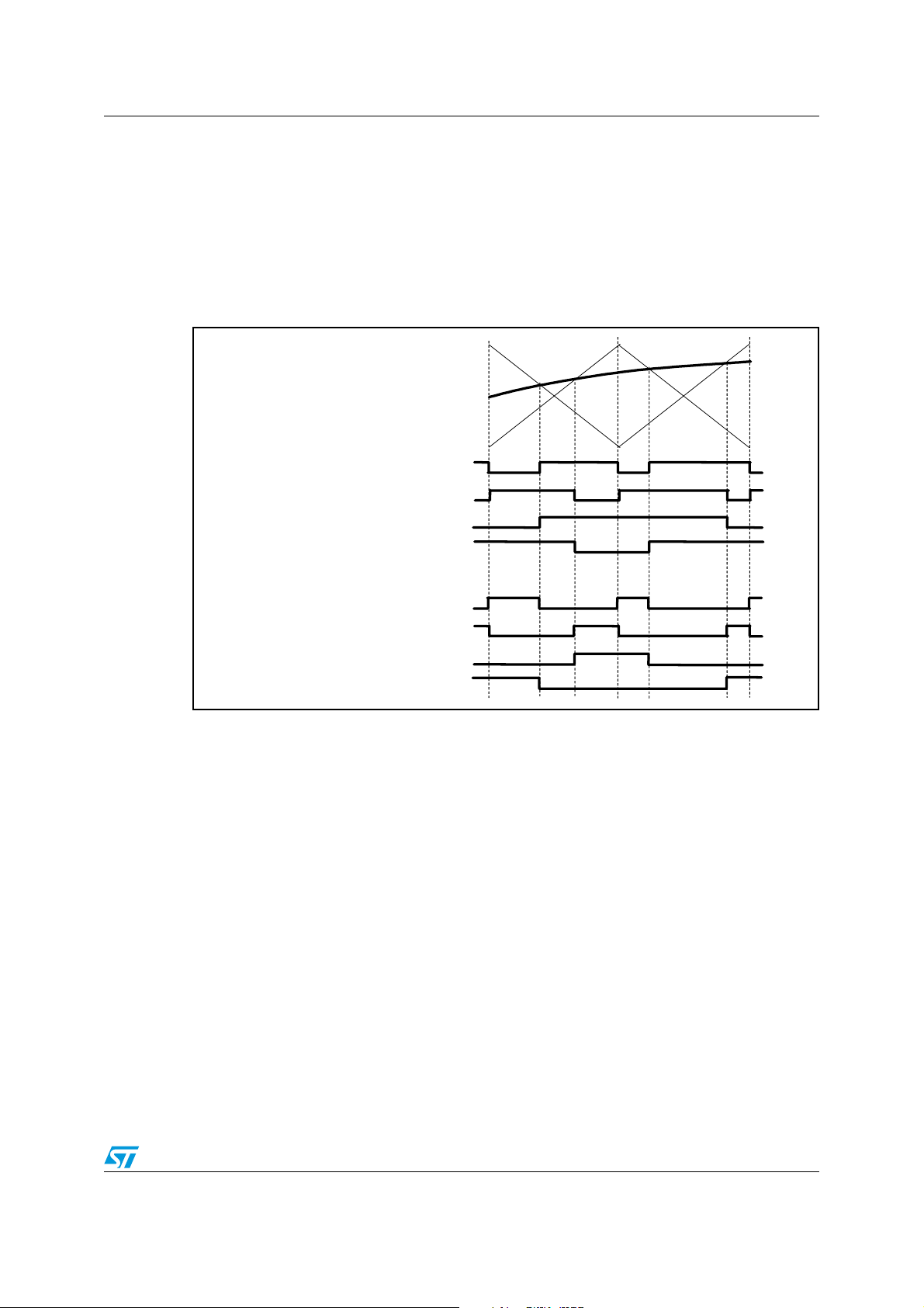
STA321 FFX
PWM output B can be similarly modulated via bits PM_nB:
z with the wave starting from level 1 at the beginning of the period, and falling to level 0
when the audio signal intersects the down-carrier;
z with the wave starting from level 0 at the beginning of the period, and rising to level 1
when the audio signal intersects the up-carrier;
The hybrid mode is the toggling between the two methods of modulation for each PWM
period.
Figure 30. PWM modes for outputs A and B
up
00: dn -> rising
up
dn
dn
PWM mode
for output A
01: up -> falling
10: hybrid 1
11: hybrid 2
00: dn -> falling
PWM mode
for output B
01: up -> rising
10: hybrid 1
11: hybrid 2
The various single output modulation schemes can be combined together on the two
outputs to get the desired differential modulation schemes.
Doc ID 15351 Rev 3 53/157
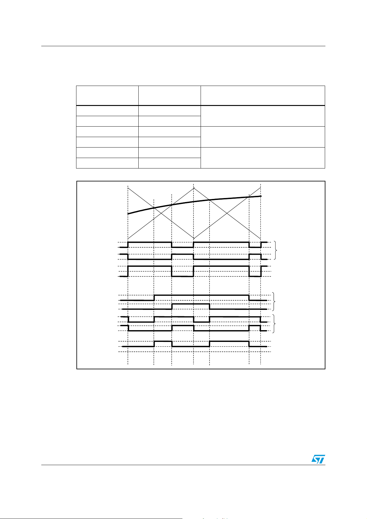
FFX STA321
In particular, for the traditional schemes (binary, phase shift), and the new one (new phase
shift modulation) the mode bits must be set according to Ta ble 2 3 below.
Table 23. Modulation type with register programming
Register bit
PWMOnCFG1.PM_nA
Register bit
PWMOnCFG2.PM_nB
Resulting modulation
00 00
binary
01 01
10 10
phase shift
11 11
00 01
new phase shift
01 00
Figure 31. Modulation waveforms corresponding to Tabl e 23
PWM mode
A: 01
B: 01
Binary
A - B
A: 10
B: 10
A: 00
B: 01
Phase shift
New phase
shift
A-B
54/157 Doc ID 15351 Rev 3

STA321 FFX
7.3 PWM shift feature
In new phase shift modulation it is possible to shift one output with respect to the other one.
This can reduce the noise generated by the simultaneous switching of two or more outputs.
The shift is performed through by programming bits PS_nA and PS_nB in registers
PWMOnCFG1-2 (where n is the number, 1 to 4, of the output) beginning on page 91.
Figure 32. New phase shift modulation with shift feature
dn up
’
up
without
shift
with
shift
A
B
A- B
A
B
A- B
Doc ID 15351 Rev 3 55/157

FFX STA321
7.4 Ternary mode
The ternary mode feature is also available. It is activated by bits TERNARY_n in registers
PWMOnCFG0 beginning on page 91 (where n is the number, 1 to 4, of the output).
This feature overrides the PWM mode bits settings PM_nA and PM_nB.
Figure 33. Ternary modulation
PWM mode
A: 10
TERNARY_n
= 0
B: 10
A: 00
B: 01
A: 10
B: 10
TERNARY_n
= 1
A: 00
B: 01
7.5 Minimum pulse limitation
The FFX modulator has a minimum pulse limitation feature which has a double purpose:
z to limit the maximum/minimum duty cycle when the audio signal is near to full scale;
z to have the commutations on the same channel outputs A and B separated by a
minimum pulse distance.
The first feature is always enabled.
The second feature is enabled with register bit PWMOnCFG0.MP_ZERO_n, where n is the
output 1 to 4. It is possible to prevent the commutations on outputs A and B to happen
exactly at the same time using bit AZPLS_n. The minimum pulse size is determined by the
number of system clock (98.304 MHz) periods programmed in bits MIN_PLS_n[3:0].
Phase
shift
New
phase
shift
Ternary
56/157 Doc ID 15351 Rev 3
STA321 FFX
7.6 Headphone modulation
The FFX modulator can be used for driving a headphone load with the common terminal
available, together with left and right terminals.
In this case it is possible to drive the common terminal with a 50% fixed duty cycle square
wave coming from output B of the modulator, by setting bit HALFB_n to 1, and the left and
right terminals from the output A of two different channels. For the three outputs used in this
way bits PM_nA and PM_nB can be 00 or 01.
Figure 34. Modulation for headphones
Left
Common
Right
Output 0A
Output 0B
Output 1A
Left
Common
Right
Doc ID 15351 Rev 3 57/157

FFX STA321
7.7 pfStart™ operation
In order to avoid pop noise the bypass capacitor, situated between the filtered amplifier
output and the load in single-ended applications, needs to be pre-charged to half of the
power supply voltage. This is usually done by connecting a resistive partition to the output
and then disconnecting it at the end of the charging phase (see the analog pop free
description in section 9).
In the STA321 the FFX digital pop-free feature allows the digital pre-charging of the bypass
capacitor using the amplifier instead of a resistive partition. This active pre-charge is also
faster than the resistive partition method. The digital pop-free function can be independently
set on both power stages, that is, the CMOS bridge stage using bit CB_PFDIG and the
embedded amplifier stage using bit EA_PFDIG in register FFXCFG2 on page 83.
Registers CB_PFRAMP1-6 beginning on page 97 and EA_PFRAMP1-6 beginning on page
99 control the charging function. The register usage is given in the following description.
The capacitor is charged from zero to half the supply voltage with the PWM signal. By
applying a suitable ramp to the input of the modulator the PWM signal begins from near 0%
duty cycle to 50% duty cycle.
The method is based on a slow ramp signal (from ground to V
/ 2), implemented using
CC
both pulse density modulation (PDM) and pulse width modulation (PWM). At the beginning
of the ramp PDM is used starting from an initial value set by bits CBRMPINI and EARMPINI,
and then switching to PWM when reaching a threshold value set by bits CBRMPTH and
EARMPTH.
The total ramp time can be modified via bits EATIM_RMP and CBTIM_RMP.
Figure 35. Digital pop-free ramp implementation
0000 …000
Ramp
value
Output
RAMP_THOLD
RAMP_INIT
1000 …000
0
PDM
PWM
The PDM is realized with a noise shaper circuit, where the sampling time (Td) of the noise
shaper is equal to the minimum pulse size set by bits CBRMP_MP and EARMP_MP.
58/157 Doc ID 15351 Rev 3

STA321 FFX
7.8 PWM00 output
Pin PWM00 is an additional output with a maximum driving capability of 2 mA to control an
external bridge or external operational amplifier.
By default, PWM00 is tied to logical 0. When register bit CKOCFG[0] is set to 1 then any
FFX PWM channel output can be mapped to it.
When the CMOS bridge is in standby the output PWM00 is, by default, turned off. However,
it is possible to have the FFX signal PWM3A as the PWM00 output by using bit 3 of register
FFXCFG0 on page 82, and this whatever the status of power-down or the 3-state signals of
both bridges, even if they are different from the normal operating mode where the output is 0
when in power-down or 3-state mode.
Doc ID 15351 Rev 3 59/157

CMOS power stage STA321
8 CMOS power stage
The CMOS half-bridge circuit of Figure 36 is a single channel analog output power stage.
There are three such output stages in the STA321, one for each of the outputs OUT1-3.
The switching mode is regulated by the logic circuit which ensures that the MOSFETs are
switched in such a way as to avoid (or minimize) conditions where both the PMOS and the
NMOS are conducting at the same time.
The input is a 1.8-V to 3.3-V level shifter followed by some combinational logic.
Figure 36. CMOS half bridge block diagram
VDD VCC33 VCCx
FaultN
OutN
FFX-ch N
Powerdown
Tristate
PopFree
Table 24. CMOS bridge signal descriptions
Level
shifter
GNDx
GND33GND
Enable
logic
Logic
GND33
Vcc33
Driver P
Driver N
Fault
Pop-free
Power
Pin Name Direction Description
FFX-ch In Digital audio signal coming from FFX block
Powerdown In Powerdown signal coming from the FFX block
Tristate In 3-state signal from the FFX block
PopFree In Pop-free signal from the FFX block
Fault Out Short-circuit fault output feedback signal to digital core (active low)
Out Out Channel half-bridge analog output
VCC33/GND33 Supply Pre-driver analog supply
VDD/GND Supply Digital core supply generated by internal regulator
VCCx/GNDx Supply Half-bridge power supply
60/157 Doc ID 15351 Rev 3

STA321 CMOS power stage
The CMOS bridge power rating can be calculated using the following formulas:
P (<1%) = (R
P (<1%) = (R
/ 2) * (M * VCC / 2 / (RL + 2 * RDS))2 for BTL
L
/ 2) * (M * VCC / 2 / (RL + RDS))2 for single ended
L
P (10%) = 1.28 * P(<1%)
where R
is composed of the MOST R
DS
and the board and connector parasitic
DSON
resistances (including power supplies and coils) and M is the modulation index obtained
from
M = 1 - 2 * (MIN_PLS_n + 1) / f
where MIN_PLS_n is the value in register PWMOnCFG0 for channel n, f
frequency of the FFX clock and τ
is the PWM clock period (384 kHz or 768 kHz selected by
S
clk_ffx
/ τ
S
is the
clk_ffx
register bit FFXCFG2.PWM_FREQ).
For the CMOS bridge, MIN_PLS_n can be set to 0; this gives M = 0.9922.
Table 25. Power output (at 1% THD) in headphone mode
Load, RL in Ω Power, P in mW (for 3.3-V supply)
16 70
32 32
The analog pop_free function is available in the CMOS bridge circuit by setting the
appropriate bridge start-up as per Ta bl e 2 6 . The CMOS bridge enable and pop-free signals
are generated from the three signals Powerdown, Tristate and PopFree provided by the
digital core and controlled/configured through register bits FFXCFG1.CB_STBY,
FFXCFG1.CB_TRISTn and PFEFAULT.PFEn for the three outputs, n = 1 to 3.
Figure 37. Analog pop-free schematic
VCCx
OutN
PFE & not(Tristate) & Powerdown
GNDx
Doc ID 15351 Rev 3 61/157

CMOS power stage STA321
Table 26. Logic circuit at bridge input
Powerdown Tristate PopFree Pop-free resistors Bridge status
000Disconnected3-state
001Disconnected3-state
101Connected 3-state
111DisconnectedOn
110DisconnectedOn
At the appropriate time the two pop-free resistors allow the bypass capacitor to be charged
to V
/ 2. The STA321 generates automatically the bridge start-up and switch-off
CCx
sequence to provide the correct charging. The time TT in Figure 38 below is set using
registers CBTTF0-1 and CBTTP0-1. TT must be chosen for the specific application
depending on the decoupling capacitor, load and power supply.
After powerdown is applied again the decoupling capacitor discharges slowly due to
capacitor leakage.
The analog pop-free implementation cannot be used with the digital pfStart implementation
Both analog and digital pop-free features must be disabled if binary headphone modulation
is used.
Figure 38. Analog pop-free start-up and switch-off sequence
Powerdown
PFE
TT
TT
Tristate
V(capacitor)
Vcc / 2
The CMOS bridge circuit includes over-current protection. The FAULT signal indicates to the
output the status of the over-current condition due to a short circuit. The over-current
thresholds detected by the CMOS bridge are fixed at 1.8 A.
62/157 Doc ID 15351 Rev 3

STA321 Fault detection and recovery
9 Fault detection and recovery
9.1 External amplifier
When Fault is reported on pin EAFTN and bit EA_TSFT_ON of register FFXCFG2 on
page 83 is active, then pin EATSN is reset to 0 and the embedded bridge outputs are put in
the high-impedance state. When the fault signal disappears (that is, goes to 1) the
embedded bridge is kept in 3-state for a time defined in register EATTF0-1 on page 86, after
which time the outputs recover.
9.2 CMOS bridge
When Fault is reported to the digital core and CB_TSFT_ON of register FFXCFG2 on
page 83 is active then the tristate is activated thus putting the STA321 OUTn outputs in the
high-impedance state. When the fault signal disappears, the CMOS bridge is kept in 3-state
status for a time defined in register CBTTF0-1 on page 88, after which time the outputs
recover.
Doc ID 15351 Rev 3 63/157

ADC STA321
10 ADC
10.1 Description
The STA321 analog input is provided through a low-power, low-voltage complete low-cost
analog-to-digital converter front end designed for stereo audio applications. It includes
programmable gain amplifier, anti-aliasing filter, low-noise microphone biasing circuit, a third
order MASH2-1 delta-sigma modulator, a digital decimating filter and a 1st-order
DC-removal filter.
The ADC works with either a microphone input or a line input, selected using bit
ADC_INSEL in register ADCCFG0 on page 133.
A programmable gain amplifier (PGA) is available in microphone-in mode giving the
possibility to amplify the signal from 0 to 42 dB in steps of 6 dB using register bit
ADCCFG0.ADC_PGA.
The ADC specifications are given in Table 6 on page 14.
Figure 39. ADC front-end block diagram
INL 1
INL 2
INR 2
INR 1
00
10
10
00
ADCCFG1[7:6]
PGA
PGA
1
0
ADCINSEL[4]
0
1
ADC left
ADC right
16 bits
16 bits
64/157 Doc ID 15351 Rev 3
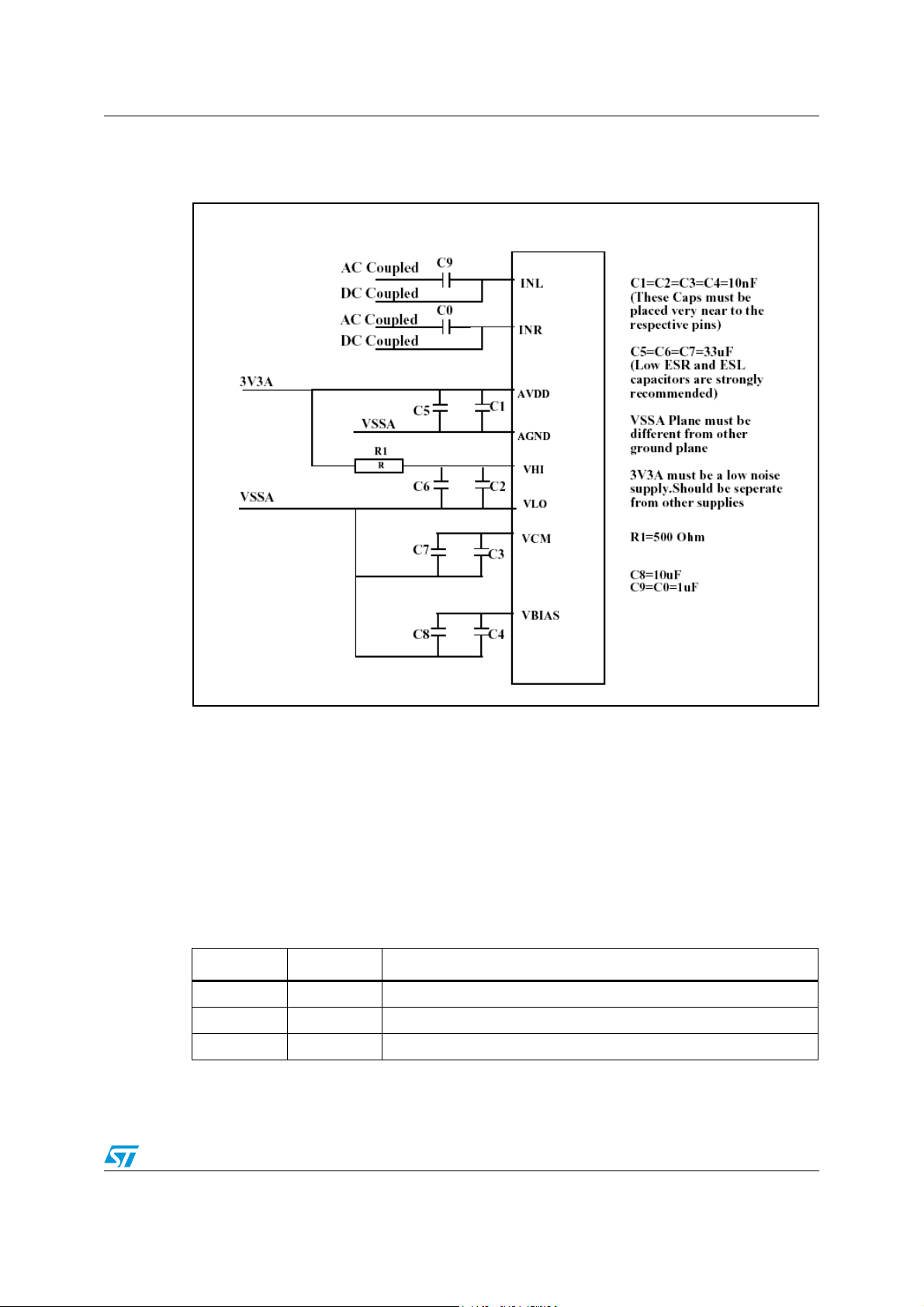
STA321 ADC
10.2 Application schematic
Figure 40. Typical connections for power supplies and inputs
10.2.1 Configuration example
This is an example of the register setup for the ADC inputs. It is assumed that every
peripheral is already configured and working correctly.
There are other configuration examples to help you get started please refer to other
chapters and also to Chapter 14: Register description on page 77 in order to get all the
necessary and complementary details.
Ta bl e 2 7 shows the register settings for selecting INL2 and INR2 as input source for SRC
and SAI_out1 and using the PGA with a 12-dB gain.
Table 27. Example register settings for ADC
Register Value Description
ADCCFG1 0x40 Selecting INL2 and INR2 as sources
ADCCFG0 0x52 PGA Gain = +12 dB, PGA enabled, ADC clock on
P2SDATA 0x40 ADC Data routed also to the SAI_out
Doc ID 15351 Rev 3 65/157

Serial audio interface STA321
11 Serial audio interface
The data on pins SDATAI, SDATAO, LRCLKI and LRCLKO are always synchronous with the
bit clock. The data on these pins changes with the BICLK active (or clocking) edge.
The BICLK strobe edge latches the data SDATAI, SDATAO, LRCLKI, LRCLKO; thus this
data should be stable near the BICLK strobe edges. The slave device uses the strobe edges
to latch the serial data internally.
The active and strobe edges can be selected to be the rising edge or the falling edge by
appropriately programming register bits SAI_IN1_CFG0[7], SAI_OUT_CFG0[7] and
SAI_IN2_CFG0[7].
The serial-to-parallel interface and the parallel-to-serial interface can have different
sampling rates. Figure 41 shows a typical setup.
Figure 41. SAI typical sampling rates
Fs = CLK / 1024
SAI_in
Fs = 8 - 192 kHz Fs = CLK / 1024
Sample rate
converter
96 kHz
Processing
Fs = CLK / 1024
96 kHz
SAI_out
or
Fs = CLK / 2048
96 kHz or
48 kHz
11.1 Master mode
In this mode BICLKI/BICLKO and LRCLKI/LRCLKO are configured as outputs and are
generated by the core.
Figure 42. Timing diagram for master mode
Biclki/
Biclko
BICLKI
BICLKO
LRCLKI
LRCLKO
SDATAO
SDATAI
CLK 98 MHz
PLL
t
DST
t
DHT
t
t
DDA
DL
66/157 Doc ID 15351 Rev 3

STA321 Serial audio interface
Table 28. Timing parameters for master mode
Symbol Parameter Min Typ Max Unit
t
DL
t
DDA
t
DST
t
DHT
LRCLKI/LRCLKO propagation delay from BICLK active
edge
SDATAI propagation delay from BICLKI/O active edge 0 - 15 ns
SDATAO setup time to BICLKI/O strobing edge 10 - - ns
SDATAO hold time from BICLKI/O strobing edge 10 - - ns
11.2 Slave mode
In this mode BICLKI/O and LRCLKI/O are configured as inputs and supplied by the external
peripheral.
Figure 43. Timing diagram for slave mode
BICLKI
BICLKO
LRCLKI
LRCLKO
SDATAO
t
BCH
t
BCy
t
t
BCL
DS
t
LRH
t
LRSU
0 - 10 ns
t
DH
SDATAI
t
DD
Table 29. Timing parameters for slave mode
Symbol Parameter Min Typ Max Unit
t
BCy
t
BCH
t
BCL
t
LRSU
t
LRH
t
DS
t
t
DH
DD
BICLK cycle time 50 - - ns
BICLK pulse width high 20 - - ns
BICLK pulse width low 20 - - ns
LRCLKI/LRCLKO setup time to BICLK strobing edge 10 - - ns
LRCLKI/LRCLKO hold time to BICLK strobing edge 10 - - ns
SDATAO setup time to BICLK strobing edge 10 - - ns
SDATAO hold time to BICLK strobing edge 10 - - ns
SDATAI propagation delay from BICLK active edge 0 - 10 ns
Doc ID 15351 Rev 3 67/157

Serial audio interface STA321
11.3 Serial formats
Different audio formats are supported in both master and slave modes. Clock and data
configurations can be customized to match most of the serial audio protocols available on
the market.
Data length can be customized for 8, 16, 24 or 32 bits.
11.3.1 Right justified
Figure 44. Right justified serial format
LRCLKI
LRCLKO
BICLKI
BICLKO
SDATAO
SDATAI
11.3.2 Left justified
Figure 45. Left justified serial format
LRCLKI
LRCLKO
BICLKI
BICLKO
SDATAO
SDATAI
68/157 Doc ID 15351 Rev 3

STA321 Serial audio interface
11.3.3 DSP
Figure 46. DSP serial format
LRCLKI
LRCLKO
BICLKI
BICLKO
Right
SDATAO
SDATAI
Left
11.3.4 I2S
Figure 47. I2S serial format
LRCLKI
LRCLKO
BICLKI
BICLKO
SDATAO
SDATAI
3 nn
11.3.5 PCM/IF (non-delayed mode)
z MSB first
z 16-bit data.
Figure 48. PCM (non-delayed) serial format
Any width
LRCLKI
LRCLKI
LRCLK
LRCLKO
BICLKI
BICLKO
BICLKI
BICLKO
-1
1 2 3 n n
-1
SDATAO
SDATAI
1 2 3 nn
-1
SDATAO/
SDATAI
Doc ID 15351 Rev 3 69/157

Serial audio interface STA321
11.3.6 PCM/IF (delayed mode)
z MSB first
z 16-bit data.
Figure 49. PCM (delayed) serial format
LRclki/
LRCLKI
LRclko
LRCLKO
BIclki/
BIclko
BICLKI
BICLKO
SDATAO/
SDATAI
SDATAO
SDATAI
1 2 3 nn
-1
70/157 Doc ID 15351 Rev 3

STA321 Serial audio interface
11.4 Invalid detection
STA321 has an invalid input detection feature that can detect an invalid serial interface bit
clock or frame clock and then mute the processing channels to avoid any speaker or
headphone damage and, moreover, to avoid loud audible transients which may be
discomforting to the listener. The control is active only for the SAI input. The configuration
programmed in bits 0, 1 and 2 of register FFXCFG0 on page 82 is applicable to both SAI1
and SAI2 whilst the checks are independent for each interface. The mute on the processing
channel is asserted depending on the input interface mapping.
Figure 50 shows the invalid detection schematic. Here, two different checks are available.
The first one is enabled by register bit FFXCFG0.BAD_CKS_M and evaluates the ratio of
BICLK and LRCLK. The resulting number must be the same as that written in bits
S2Pn_BOS (for example, 32 * f
SAI_IN2_CFG1, otherwise the channels are muted.
The second check is enabled by register bit FFXCFG0.MIS_BICK_M and is related to the
presence of BICLK. Basically, a 8-bit watchdog counter decrements, starting from 0xFF, with
each edge of clk_proc. The counter is reset to 0xFF at each BICLK edge; so, if the
watchdog counter ever reaches 0x00, a missing bit clock error is signalled and the mute
command is issued.
Figure 50. Invalid input detection schematic
or 64 * fS) in registers SAI_IN1_CFG1 on page 123 and
S
00
mute ch0
clk_proc
Is
alive?
BICLKI1
LRCLKI1
LRCLKI2
BICLKI2
Ratio
calculator
Ratio
calculator
Is
alive?
MIS_BICK_M
=
BAD_CKS_M
S2P1_BOS
S2P2_BOS
BAD_CKS_M
=
MIS_BICK_M
clk_proc
MUTE0
OR
MUTE1
MUTE0
MUTE1
MUTE2
MUTE3
MUTE2
OR
MUTE3
01
1x
SRC1_INSEL
00
mute ch1
01
1x
00
mute ch2
01
1x
SRC2_INSEL
00
mute ch3
01
1x
Doc ID 15351 Rev 3 71/157
Headphone detection STA321
12 Headphone detection
The headphone detector circuit, shown in Figure 51, is made with two schmitt-trigger
comparators (with different thresholds) which sense the value of the HPDECT input voltage
and modifies the HP_DET1 or the HP_DET2 level as given in Ta bl e 3 0 and Table 3 1 below.
The comparators are enabled or disabled with bits E_HP1 and E_HP2 in register HPDET2
on page 138
Table 30. Headphone 1 detector
E_HP1
(register HPDET2)
HP-jack status HP_DET voltage HP_DET1
Status register bit
HPDST.HP_DET_FILT
1 Unplugged Low 0 -
1 Plugged High 1 -
0XX1-
Table 31. Headphone 2 detector
E_HP2
(register HPDET2)
HP-jack status HP_DET voltage HP_DET2
Status register bit
HPDST.HP_DET_FILT
1 Unplugged Low 1 -
1 Plugged High 0 -
0XX1-
The comparator output status is provided via bits 1 and 0 of register HPDET2 on page 138.
One of the comparator outputs is then selected with register bit HPDET1.HPD_SEL, and
that signal is passed through a digital debouncing filter and supplied to the FFX modulator.
The PWM outputs are then modified depending on the settings of register bits
HPDST.HP_DET_FILT and HPDET1.HPD_ACT_MODE.
72/157 Doc ID 15351 Rev 3
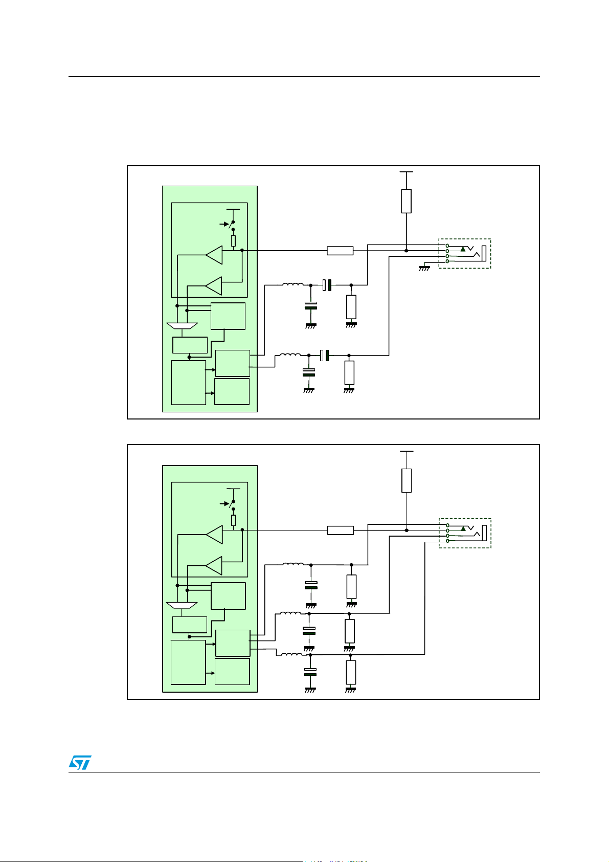
STA321 Headphone detection
12.1 Applications circuits
Two applications circuits are given here, one for the binary single-ended application and one
for the binary headphone application.
Figure 51. Headphone detection circuit for single-ended configuration
VCC33
VCC33
100 k
TUD_EN
HP_DET1
HP_DET2
Filter
I2C
HP_DET_FILT
CMOS
bridge
HP_DET
L1
L2
5 k
1 k
1 k
EAPWM
FFX
modulator
out
Figure 52. Headphone detection circuit for binary HP configuration
VCC33
VCC33
100 k
TUD_EN
HP_DET1
HP_DET2
HP_DET
L1
I2C
5 k
1 k
L2
hp_det_filt
Filter
CMOS
bridge
EAPWM
FFX
modulator
out
L3
1 k
1 k
Doc ID 15351 Rev 3 73/157

Headphone detection STA321
12.2 Configuration example
This is an example of the register setup for headphones detection. It is assumed that every
peripheral is already configured and working correctly.
There are other configuration examples to help you get started please refer to other
chapters and also to Chapter 14: Register description on page 77 in order to get all the
necessary and complementary details.
Ta bl e 3 2 and Tabl e 3 3 below give a possible setup for the headphones detection
configurations shown in Figure 51 and Figure 52, respectively.
Table 32. Headphone detection configuration sequence for binary SE
Register Value Description
MISC on page 135
0x21 Enable core clock
PLLB on page 136 0x00 Use PLL clock
User FFX and CMOS bridge configuration
HPDET2 on page 138 0x80 Disable the HP_DET pull-up
HPDET1 on page 137 0x57
Use HP1 for hpdet filter; polarity = high; action =
mute; mod = binary SE; average time 170 ms.
HPDET2 on page 138 0x80 Select E_HP1 comparator
FFXCFG1 on page 81 0x00 Remove the tristate from the bridges
Table 33. Headphone detection configuration sequence for binary headphone
Register Value Description
MISC on page 135
0x21 Enable core clock
PLLB on page 136 0x00 Use PLL clock
User FFX and CMOS bridge configuration
HPDET2 on page 138 0x80 Disable the HP_DET pull-up
HPDET1 on page 137 0x5F
Use HP1 for hpdet filter; polarity = high; action =
mute; mod = binary HP; average time 170 ms.
HPDET2 on page 138 0x80 Select E_HP1 comparator
FFXCFG1 on page 81 0x00 Remove the tristate from the bridges
Note: The pullup on HPDET pad must always be disabled before using the HPDET function.
Note: Comparator 1 and comparator 2 cannot be enabled simultaneously.
74/157 Doc ID 15351 Rev 3

STA321 I2C interface
13 I2C interface
13.1 Communication protocol
13.1.1 Data transition and change
Data changes on the SDA line must only occur when the SCL clock is low. SDA transition
while the clock is high is used to identify a START or STOP condition.
13.1.2 Start condition
START is identified by a high to low transition of the SDA bus while the clock signal, SCL, is
stable in the high state. A START condition must precede any command for data transfer.
13.1.3 Stop condition
STOP is identified by a low to high transition on the SDA bus while the clock signal, SCL, is
stable in the high state. A STOP condition terminates communication between STA321 and
the bus master.
13.1.4 Data input
During the data input the STA321 samples the SDA signal on the rising edge of clock SCL.
For correct device operation the SDA signal must be stable during the rising edge of the
clock and the data can change only when the SCL line is low.
13.1.5 Device addressing
To start communication between the master and the STA321, the master initiates with a
start condition. Following this, the master sends 8 bits (MSB first) on the SDA line which
corresponds to the device select address and read or write mode.
The 7 MSBs are the device address identifiers, corresponding to the I
the STA321 the I
2
C interface has the device address 0x30.
After a START condition the STA321 identifies the device address and if a match is found,
acknowledges the identification on SDA bus during the 9th bit time. The byte following the
device identification byte is the internal space address.
13.1.6 Write operation
Following the START condition the master sends a device select code with the RW bit set
to 0. After the STA321 acknowledge, the master sends the byte of internal address. On
receiving the internal byte address the STA321 responds with acknowledge.
Byte write
2
C bus definition. In
In the byte write mode the master sends one data byte, this is acknowledged by the
STA321. The master then terminates the transfer by generating a STOP condition.
Doc ID 15351 Rev 3 75/157

I2C interface STA321
Multi-byte write
The multi-byte write mode starts from any internal address. The master generates a STOP
condition to terminate the transfer.
13.1.7 Read operation
Current address byte read
Following the START condition the master sends a device select code with the RW bit set
to 1. The STA321 acknowledges and then responds by sending one byte of data. The
master then terminates the transfer by generating a STOP condition.
Current address multi-byte read
The multi-byte read mode start from any internal address. Data bytes are read from
sequential addresses within the STA321. The master acknowledges each data byte read
and then generates a STOP condition to terminate the transfer.
Random address byte read
Following the START condition the master sends a device select code with the RW bit set
to 0. The STA321 acknowledges and then the master writes the internal address byte. After
receiving, the internal byte address the STA321 again responds with an acknowledge. The
master then initiates another START condition and sends the device select code with the
RW bit set to 1. The STA321 acknowledges this and then responds by sending one byte of
data. The master then terminates the transfer by generating a STOP condition.
Random address multi-byte read
The multi-byte read modes start from any internal address. Data bytes are read from
sequential addresses within the STA321. The master acknowledges each data byte read
and then generates a STOP condition to terminate the transfer.
Figure 53. I
Figure 54. I2C read operations
2
C write operations
76/157 Doc ID 15351 Rev 3

STA321 Register description
14 Register description
Table 34. Register summary
RegisterAddr76543210
FFXCFG1 0x00
FFXCFG0 0x01
FFXCFG2 0x02
PWMMAP1 0x03
PWMMAP2 0x04
PWMMAP3 0x05
EATTF0 0x06
EATTF1 0x07
EATTP0 0x08
EATTP1 0x09
CBTTF0 0x0A
CBTTF1 0x0B
CBTTP0 0x0C
CBTTP1 0x0D
FFXST 0x0E
POWST 0x0F
POWST1 0x10
PWMO1CFG0 0x11
PWMO1CFG1 0x12
PWMO1CFG2 0x13
PWMO2CFG0 0x14
PWMO2CFG1 0x15
PWMO2CFG2 0x16
PWMO3CFG0 0x17
PWMO3CFG1 0x18
PWMO3CFG2 0x19
PWMO4CFG0 0x1A
PWMO4CFG1 0x1B
PWMO4CFG2 0x1C
CB_PFRAMP1 0x20
CB_PFRAMP2 0x21
CB_PFRAMP3 0x22
CB_PFRAMP4 0x23
CB_PFRAMP5 0x24
CB_PFRAMP6 0x25
EA_PFRAMP1 0x26
EA_PFRAMP2 0x27
EA_STBY CB_STBY EA_TRIST FFX_ULCK_PLL CB_TRIST2 CB_TRIST1 CB_TRIST0
MUTE3 MUTE2 MUTE1 MUTE0 PWM00_3A BAD_IN_M BAD_CKS_M MIS_BICK_M
RESET
_NOISH
CB3_MAP[0] PWM00_MAP[2:0] EA1A_MAP[2:0] EA1B_MAP[2]
EA_MPWM CB_MPWM EARMP_ST[1:0] CBRMP_ST[1:0] EABINSS_AC CBBINSS_AC
Reserved CB_PD CB_FT[2:0] CB_TS[2:0]
AZPLS_1 TERNARY_1 HALFB_1 MP_ZERO_1 MIN_PLS_1[3:0]
AZPLS_2 TERNARY_2 HALFB_2 MP_ZERO_2 MIN_PLS_2[3:0]
AZPLS_3 TERNARY_3 HALFB_3 MP_ZERO_3 MIN_PLS_3[3:0]
AZPLS_4 TERNARY_4 HALFB_4 MP_ZERO_4 MIN_PLS_4[3:0]
PWM_FREQ NS_ORD[1:0] EA_TSFT_ON CB_TSFT_ON EA_PFDIG CB_PFDIG
CB1_MAP[2:0] CB2_MAP[2:0] CB3_MAP[2:1]
EA1B_MAP[1:0] EA2A_MAP[2:0] EA2B_MAP[2:0]
EATTF[7:0]
EATTF[7:0]
EATTP[15:8]
EATTP[7:0]
CBTTF[15:8]
CBTTF[7:0]
CBTTP[15:8]
CBTTP[7:0]
Reserved EA_TW EA_PD EA_FT EA_TS
PM_1A[1:0] PS_1A[5:0]
PM_1B[1:0] PS_1B[5:0]
PM_2A[1:0] PS_2A[5:0]
PM_2B[1:0] PS_2B[5:0]
PM_3A[1:0] PS_3A[5:0]
PM_3B[1:0] PS_3B[5:0]
PM_4A[1:0] PS_4A[5:0]
PM_4B[1:0] PS_4B[5:0]
CBRMP_MP[5:0] Reserved
CBRMPINI[15:8]
CBRMPINI[7:0]
CBTIM_RMP[3:0] Reserved
CBRMPTH[15:8]
CBRMPTH[7:0]
EARMP_MP[5:0] Reserved
EARMPINI[15:8]
Doc ID 15351 Rev 3 77/157

Register description STA321
Table 34. Register summary (continued)
RegisterAddr76543210
EA_PFRAMP3 0x28
EA_PFRAMP4 0x29
EA_PFRAMP5 0x2A
EA_PFRAMP6 0x2B
SRC1STATE 0x30
SRC2STATE 0x31
I2CB0_TOP 0x51
I2CB0_MID 0x52
I2CB0_BOT 0x53
I2CB1_TOP 0x54
I2CB1_MID 0x55
I2CB1_BOT 0x56
I2CB2_TOP 0x57
I2CB2_MID 0x58
I2CB2_BOT 0x59
I2CA1_TOP 0x5A
I2CA1_MID 0x5B
I2CA1_BOT 0x5C
I2CA2_TOP 0x5D
I2CA2_MID 0x5E
I2CA2_BOT 0x5F
PROCCTRL 0x60
START_ADD2 0x61
START_ADD 0x62
ROM_REMAP 0x6F
BYP_EN_CH0 0x70
EFFS_EN_CH0 0x71
BYP_EN_CH1 0x72
EFFS_EN_CH1 0x73
BYP_EN_CH2 0x74
EFFS_EN_CH2 0x75
BYP_EN_CH3 0x76
EFFS_EN_CH3 0x77
BASS_SEL0_R 0x78
BASS_SEL1_R 0x79
BASS_SEL2_R 0x7A
BASS_SEL3_R 0x7B
TREB_SEL0_R 0x7C
TREB_SEL1_R 0x7D
TREB_SEL2_R 0x7E
EATIM_RMP[3:0] Reserved
SRC1_BYP[1:0] SRC_1_LOCK SRC1_FISFO[4:0]
SRC1_BYP[1:0] SRC_1_LOCK SRC1_FISFO[4:0]
Reserved RA Reserved WA W1
Reserved ENAB_PRE3 ENAB_PRE2 ENAB_PRE1 ENAB_PRE0 ENAB_POST ENAB_PRMIX ENAB_DELAY
Reserved EROM09 EROM08
Reserved EROM19 Reser ved
Reserved EROM29 EROM28
Reserved EROM39 Reser ved
Reserved BASS_EN0 BASS_SEL0
Reserved BASS_EN1 BASS_SEL1
Reserved BASS_EN2 BASS_SEL2
Reserved BASS_EN3 BASS_SEL3
Reserved TREB_EN0 TREB_SEL0
Reserved TREB_EN1 TREB_SEL1
Reserved TREB_EN2 TREB_SEL2
EARMPINI[7:0]
EARMPTH[15:8]
EARMPTH[7:0]
I2CB0[23:16]
I2CB0[15:8]
I2CB0[7:0]
I2CB1[23:16]
I2CB1[15:8]
I2CB1[7:0]
I2CB2[23:16]
I2CB2[15:8]
I2CB2[7:0]
I2CA1[23:16]
I2CA1[15:8]
I2CA1[7:0]
I2CA2[23:16]
I2CA2[15:8]
I2CA2[7:0]
Reserved I2CSTART_A8
I2CSTART_A7_A0
Reserved
Reserved
Reserved
Reserved
78/157 Doc ID 15351 Rev 3

STA321 Register description
Table 34. Register summary (continued)
RegisterAddr76543210
TREB_SEL3_R 0x7F
SATCH0CFG1 0x90
SATCH0CFG2 0x91
SATCH0CFG3 0x92
SATCH1CFG1 0x93
SATCH1CFG2 0x94
SATCH1CFG3 0x95
SATCH2CFG1 0x96
SATCH2CFG2 0x97
SATCH2CFG3 0x98
SATCH3CFG1 0x99
SATCH3CFG2 0x9A
SATCH3CFG3 0x9B
VOLCFG 0xA0
MVOL 0xA1
VOLCH0 0xA2
VOLCH1 0xA3
VOLCH2 0xA4
VOLCH3 0xA5
SAI_IN1_CFG0 0xB0
SAI_IN1_CFG1 0xB1
SAI_OUT_CFG0 0xB2
SAI_OUT_CFG1 0xB3
SAI_IN2_CFG0 0xB4
SAI_IN2_CFG1 0xB5
AUIFSHARE 0xB6
SRCINSEL 0xB7
P2SDATA 0xB8
PLLCFG0 0xC0
PLLCFG1 0xC1
PLLCFG2 0xC2
PLLCFG3 0xC3
PLLPFE 0xC4
PLLST 0xC5
ADCCFG0 0xC6
CKOCFG 0xC7
MISC 0xC8
Reserved TREB_EN3 TREB_SEL3
SAT_EQ SAT_CH0[22:16]
SAT_CH0[15:8]
SAT_CH0[7:0]
Reserved SAT_CH1[22:16]
SAT_CH1[15:8]
SAT_CH1[7:0]
Reserved SAT_CH2[22:16]
SAT_CH2[15:8]
SAT_CH2[7:0]
Reserved SAT_CH3[22:16]
SAT_CH3[15:8]
SAT_CH3[7:0]
SVOL_ON3 SVOL_ON2 SVOL_ON1 SVOL_ON0 TIM_SVOL
MVOL
CVOL0
CVOL1
CVOL2
CVOL3
S2P1_B_STR S2P1_LR_L Reserved S2P1_MSB S2P1_DFM S2P1_MMD
S2P1_DLEN S2P1_BOS S2P1_MAP_L S2P1_MAP_R
P2S_B_STR P2S_LR_L SDATAO_ACT P2S_MSB P2S_DFM P2S_MMD
P2S_DLEN P2S_BOS P2S_MAP_L P2S_MAP_R
S2P2_B_STR S2P2_LR_L Reserved S2P2_MSB S2P2_DFM S2P2_MMD
S2P2_DLEN S2P2_BOS S2P2_MAP_L S2P2_MAP_R
Reserved SHARE_BILR
SRC1_INSEL SRC2_INSEL MUTE_SRCU Reserved
Reserved P2S_HFS P2S1_DSEL P2S2_DSEL
PLL_DPROG
PLL_STRB
PLL_BYP
_UNL
PLL_UNLOCK PLL_PWD_ST PLL_BYP_ST Reserved
CLKOUT_DIS CLKOUT_SEL CLK_FFX_ON CLK_SRC_ON
OSC_DIS S2P_FS_RNG ADC_FS_RNG P2P_IN_ADC
PLL_FR
_CTRL
PLL
_STRBBYP
BICLK2PLL PLL_PWDN
ADC_PGA ADC_INSEL ADC_STBY ADC_BYPCAL CLK_ADC_ON Reserved
PLL_DDIS PLL_IDF
PLL_FRAC[15:8]
PLL_FRAC[7:0]
PLL_NDIV
PLL
_NOPDDIV
CLK_PROC
_ON
Reserved
EAPWM_DIS PWM00ACT
CLKCORE
_ON
Doc ID 15351 Rev 3 79/157
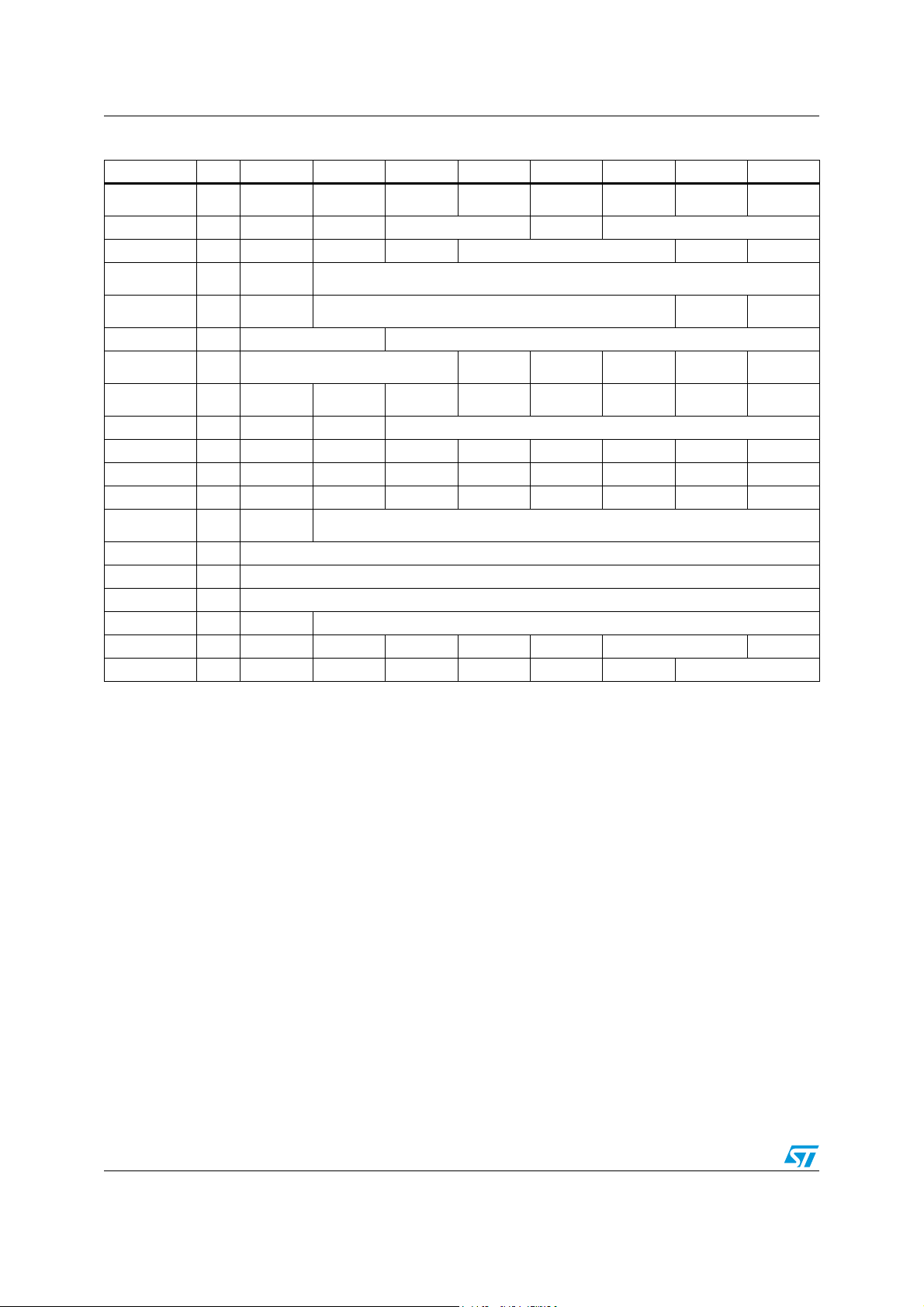
Register description STA321
Table 34. Register summary (continued)
RegisterAddr76543210
PLLB 0xC9
HPDET1 0xCA
HPDET2 0xCB
HPDST 0xCC
STBY_MODES 0xCD
ADCCFG1 0xCE
PFEFAULT 0xCF
BISTRUN0 0xD0
BISTRUN1 0xD1
BISTST0 0xD2
BISTST1 0xD3
BISTST2 0xD4
BISTST3 0xD5
ROMSIGN0 0xD6
ROMSIGN1 0xD7
ROMSIGN2 0xD8
DEBUG0 0xD9
PADST0 0xF0
PADST1 0xF1
PLL_BYP Reserved ADC_CLKSEL Reserved
P2S1
_CLKSEL
Reserved
HPD_SEL HPD_POL HPD_ACT_MODE HPD_HPMOD HPD_TIM_F
E_HP2 E_HP1 TUD_EN Reserved E_HPDET1 E_HPDET2
HPD_DET
_FILT
Reserved
PAD_PULLDIS Reserved CMP_EN_N
ADC_ANA_SEL Reserved
Reserved PFE1 PFE2 PFE3
SF1_BRUN SF2_BRUN SS1_BRUN SS2_BRUN CF_BRUN PR_BRUN
OS_BRUN DB_BRUN Reserved
SF1_BEND SF1_BBAD SF1_BFAIL SF2_BEND SF2_BBAD SF2_BFAIL SS1_BEND SS1_BBAD
SS1_BFAIL SS2_BEND SS2_BBAD SS2_BFAIL CF_BEND CF_BBAD CF_BFAIL PR_BEND
PR_BBAD PR_BFAIL OS_BEND OS_BBAD OS_BFAIL DB_BEND DB_BBAD DB_BFAIL
CF_ROM
_BEND
Reserved
CF_ROMS[7:0]
CF_ROMS[15:8]
CF_ROMS[23:16]
DBGCKO_ON DBGCKO_VAL
PAD_RSTN Reserved PAD_SCL PAD_SDA PAD_I2CDIS Reserved PAD_STBY
PAD_MUTE PAD_BICLKI PAD_LRCLKI PAD_SDATAI PAD_BICLKO PAD_LRCLKO Reserved
P2S2
_CLKSEL
RESET_EA
_FT
CF_ROM
_BRUN
Reserved
DC_STBY
_EN_N
RESET_CB
_FT
Reserved
80/157 Doc ID 15351 Rev 3

STA321 Register description
FFXCFG1
76543210
EA_STBY CB_STBY EA_TRIST FFX_ULCK_PLL CB_TRIST2 CB_TRIST1 CB_TRIST0
Address: 0x00
Type: RW
Reset: 0xD0
Description:
[7] EA_STBY
0: the external bridge is active
1: the external bridge is in standby mode
[6] CB_STBY
0: the bridge is active
1: the bridge is in standby mode
[5] EA_TRIST
0: normal behaviour
1: the external bridge is put in 3-state mode
[4:3] FFX_ULCK_PLL: behavior of the FFX modulator in the event of the PLL losing lock:
00: do nothing
01: FFX hard mute (equivalent to using pin MUTE)
10: FFX standby
11: FFX hard mute and noise-shaper reset
[2] CB_TRIST2
0: the bridge is active
1: force CMOS bridge OUT3 to 3-state
[1] CB_TRIST1
0: the bridge is active
1: force CMOS bridge OUT2 to 3-state
[0] CB_TRIST0
0: normal behaviour
1: force CMOS bridge OUT1 to 3-state
Doc ID 15351 Rev 3 81/157

Register description STA321
FFXCFG0
76543 2 1 0
MUTE3 MUTE2 MUTE1 MUTE0 PWM00_3A BAD_IN_M BAD_CKS_M MIS_BICK_M
Address: 0x01
Type: RW
Reset: 0x07
Description:
[7] MUTE3
0: normal behaviour
1: force the mute in the channel 3
[6] MUTE2
0: normal behaviour
1: force the mute in the channel 2
[5] MUTE1
0: normal behaviour
1: force the mute in the channel 1
[4] MUTE0
0: normal behaviour
1: force the mute in the channel 0
[3] PWM00_3A
0: output PWM00 is driven by FFX (default)
1: output PWM00 comes from FFX output PWM3A and is not sensitive to bridge power-down or
3-state states
[2] BAD_IN_M
Depending on the bit 0 and bit 1 settings
0: mute with a ramp
1: mute instantaneously
[1] BAD_CKS_M
0: FFX not muted
1: FFX muted if biclk and lrclk do not meet the specification
[0] MIS_BICK_M
0: FFX not muted
1: FFX will be muted if biclk is missing
82/157 Doc ID 15351 Rev 3

STA321 Register description
FFXCFG2
76543210
RESET_NOISH PWM_FREQ NS_ORD[1:0] EA_TSFT_ON CB_TSFT_ON EA_PFDIG CB_PFDIG
Address: 0x02
Type: RW
Reset: 0x2D
Description:
[7] RESET_NOISH
1: a reset is forced to the noise-shaper block
[6] PWM_FREQ
0: 4 f
(4*96 kHz = 384 kHz)
S
1: 8 fS (8*96 kHz = 768 kHz)
[5:4] NS_ORD[1:0]
Noise shape order
00: 3rd. order
01: 4th. order
10: 5th. order
[3] EA_TSFT_ON
1: if there is a fault on the external bridge, it will be put in 3-state
[2] CB_TSFT_ON
1: if there is a fault on the CMOS bridge, it will be put in 3-state
[1] EA_PFDIG
1: enable the pop-free ramp of EA
[0]
CB_PFDIG
1: enable the pop-free ramp of CB
Note: Particular care must be taken when bits NS_ORD and PWM_FREQ are changed. To avoid
any audible artifacts, these bits must be modified only with the following procedure:
1. Mute STA321 processing.
2. Change PWM_FREQ and/or NS_ORD and set RESET_NOISH = 1.
3. Configure RESET_NOISH = 0.
4. Unmute STA321 processing.
Doc ID 15351 Rev 3 83/157

Register description STA321
PWMMAP1 Processing to PWM out mapping
765432 1 0
CB1_MAP[2:0] CB2_MAP[2:0] CB3_MAP[2:1]
Address: 0x03
Type: RW
Reset: 0x08
Description:
[7:5] CB1_MAP[2:0]
CB_PWM_1 channel mapping:
000: Ch0-A 001: Ch0-B
010: Ch1-A 011: Ch1-B
100: Ch2-A 101: Ch2-B
110: Ch3-A 111: Ch3-B
[4:2] CB2_MAP[2:0]
CB_PWM_2 channel mapping
000: Ch0-A 001: Ch0-B
010: Ch1-A 011: Ch1-B
100: Ch2-A 101: Ch2-B
110: Ch3-A 111: Ch3-B
[1:0] CB3_MAP[2:1]
CB_PWM_3 channel mapping (for bit 0 see register
000: Ch0-A 001: Ch0-B
010: Ch1-A 011: Ch1-B
100: Ch2-A 101: Ch2-B
110: Ch3-A 111: Ch3-B
PWMMAP2):
84/157 Doc ID 15351 Rev 3

STA321 Register description
PWMMAP2
7 654321 0
CB3_MAP[0] PWM00_MAP[2:0] EA1A_MAP[2:0] EA1B_MAP[2]
Address: 0x04
Type: RW
Reset: 0xB9
Description:
[7] CB3_MAP[0]
CB_PWM_3 channel mapping (for bits 1 and 2 see register PWMMAP1)
[6:4] PWM00_MAP[2:0]
PWM00 channel mapping:
000: Ch0-A 001: Ch0-B
010: Ch1-A 011: Ch1-B
100: Ch2-A 101: Ch2-B
110: Ch3-A 111: Ch3-B
[3:1] EA1A_MAP[2:0]
EA_PWM_1A channel mapping:
000: Ch0-A 001: Ch0-B
010: Ch1-A 011: Ch1-B
100: Ch2-A 101: Ch2-B
110: Ch3-A 111: Ch3-B
[0]
EA1B_MAP[2]
EA_PWM_1B channel mapping (for bits 1and 0 see register PWMMAP3)
000: Ch0-A 001: Ch0-B
010: Ch1-A 011: Ch1-B
100: Ch2-A 101: Ch2-B
110: Ch3-A 111: Ch3-B
Doc ID 15351 Rev 3 85/157

Register description STA321
PWMMAP3
7 6 543210
EA1B_MAP[1:0] EA2A_MAP[2:0] EA2B_MAP[2:0]
Address: 0x05
Type: RW
Reset: 0x77
Description:
[7:6] EA1B_MAP[1:0]
EA_PWM_1B channel mapping (for bit 2 see register PWMMAP2)
[5:3] EA2A_MAP[2:0]
EA_PWM_2A channel mapping:
000: Ch0-A 001: Ch0-B
010: Ch1-A 011: Ch1-B
100: Ch2-A 101: Ch2-B
110: Ch3-A 111: Ch3-B
[2:0] EA2B_MAP[2:0]
EA_PWM_2B channel mapping:
000: Ch0-A 001: Ch0-B
010: Ch1-A 011: Ch1-B
100: Ch2-A 101: Ch2-B
110: Ch3-A 111: Ch3-B
EATTF0 External bridge tristate time from fault
76543210
EATTF[15:8]
Address: 0x06
Type: RW
Reset: 0x00
Description: The tristate time is the time between fault deasserted and 3-state removed for the
external bridge. It is calculated as EATTF[15:0] * 41.66 µs
[7:0] EATTF[15:8]
MSBs of the EA tristate time factor
86/157 Doc ID 15351 Rev 3

STA321 Register description
EATTF1 External bridge tristate time from fault
76543210
EATTF[7:0]
Address: 0x07
Type: RW
Reset: 0x03
Description: See also register
EATTF0
[7:0] EATTF[7:0]
LSBs of EA tristate time factor
EATTP0 External bridge tristate time from powerdown
76543210
EATTP[15:8]
Address: 0x08
Type: RW
Reset: 0x00
Description: This tristate time is the time between bridge powerdown removed and 3-state
removed for the external bridge. It is calculated as EATTP[15:0] * 41.66 µs
[7:0] EATTP[15:8]
MSBs of EA 3-state time after power-up factor
EATTP1 External bridge tristate time from powerdown
76543210
EATTP[7:0]
Address: 0x09
Type: RW
Reset: 0x03
Description: See also register
[7:0] EATTP[7:0]
LSBs of EA 3-state time after power-up factor
EATTP0
Doc ID 15351 Rev 3 87/157

Register description STA321
CBTTF0 CMOS bridge tristate time from fault
76543210
CBTTF[15:8]
Address: 0x0A
Type: RW
Reset: 0x00
Description: The tristate time is the time between fault deasserted and 3-state removed for the
CMOS bridge. It is calculated as CBTTF[15:0] * 41.66 µs
[7:0] CBTTF[15:8]
MSBs of CB 3-state time factor
CBTTF1 CMOS bridge tristate time from fault
76543210
CBTTF[7:0]
Address: 0x0B
Type: RW
Reset: 0x02
Description: See also register
[7:0] CBTTF[7:0]
LSBs of CB 3-state time factor
CBTTF0
CBTTP0 CMOS bridge tristate time from powerdown
76543210
CBTTP[15:8]
Address: 0x0C
Type: RW
Reset: 0x00
Description: This tristate time is the time between bridge powerdown removed and 3-state
removed for the CMOS bridge. It is calculated as CBTTP[15:0] * 41.66 µs
[7:0] CBTTP[15:8]
MSBs of CB 3-state time after power-up factor
88/157 Doc ID 15351 Rev 3

STA321 Register description
CBTTP1 CMOS bridge tristate time from powerdown
76543210
CBTTP[7:0]
Address: 0x0D
Type: RW
Reset: 0x02
Description: See also register
[7:0] CBTTP[7:0]
LSBs of CB 3-state time after power-up factor
FFXST
7 6 5432 1 0
EA_MPWM CB_MPWM EARMP_ST[1:0] CBRMP_ST[1:0] EABINSS_AC CBBINSS_AC
Address: 0x0E
Type: RO
Reset: 0xC0
Description:
[7] EA_MPWM
1: EA is in mute
[6] CB_MPWM
1: CB is in mute
EARMP_ST[1:0]: pop free ramp status
[5:4]
00: parked
11: ready
10: going to park
01: going to ready
[3:2] CBRMP_ST[1:0]: pop free ramp status
00: parked
11: ready
10: going to park
01: going to ready
[1] EABINSS_AC
1: ramp active (going to park or ready)
CBBINSS_AC
[0]
1: ramp active (going to park or ready)
CBTTP0
Doc ID 15351 Rev 3 89/157

Register description STA321
POWST Status register for external amplifier
76543210
Reserved EA_TW EA_PD EA_FT EA_TS
Address: 0x0F
Type: RO
Reset: 0x05
Description:
[7:4] Reserved
[3] EA_TW
1: EA thermal warning
[2] EA_PD
EA power-down
1:
[1] EA_FT
EA is in fault
1:
[0]
EA_TS
1: EA is in 3-state
POWST1 Status register for CMOS bridge
76543210
Reserved CB_PD CB_FT[2:0] CB_TS[2:0]
Address: 0x10
Type: RO
Reset: 0x47
Description:
[7] Reserved
[6] CB_PD
1: CMOS bridge
[5:3] CB_FT[2:0]
xx1: CMOS bridge channel 1 is in fault
x1x: CMOS bridge channel 2 is in fault
1xx: CMOS bridge channel 3 is in fault
[2:0] CB_TS[2:0]
xx1: CMOS bridge channel 1 is in 3-state
x1x: CMOS bridge channel 2 is in 3-state
1xx: CMOS bridge channel 3 is in 3-state
is in power-down
90/157 Doc ID 15351 Rev 3

STA321 Register description
PWMO1CFG0
7 6 5 4 3210
AZPLS_1 TERNARY_1 HALFB_1 MP_ZERO_1 MIN_PLS_1[3:0]
Address: 0x11
Type: RW
Reset: 0x20
Description:
[7] AZPLS_1
1: avoid zero pulse
[6] TERNARY_1
1: ternary modulation
[5] HALFB_1
1: 1B is modulated as null signal
[4] MP_ZERO_1
1:
apply the minimum pulse settings also for values near 0
[3:0] MIN_PLS_1[3:0]
minimum pulse length = clock period * (MIN_PLS_1 + 1)
PWMO1CFG1
76543210
PM_1A[1:0] PS_1A[5:0]
Address: 0x12
Type: RW
Reset: 0x00
Description: Configuration for PWM-A
[7:6] PM_1A[1:0]: PWM mode
00: generate a rising edge using a down carrier
01: generate a falling edge using an up carrier
10: hybrid mode: alternation of modes 00 and 01
11: hybrid mode: alternation of modes 01 and 00
[5:0] PS_1A[5:0]: PWM shift
The PWM waveform could be shifted by (PS_1A * clock period / 64)
Doc ID 15351 Rev 3 91/157

Register description STA321
PWMO1CFG2
76543210
PM_1B[1:0] PS_1B[5:0]
Address: 0x13
Type: RW
Reset: 0x48
Description: Configuration for PWM-B
[7:6] PM_1B[1:0]: PWM mode
00: generate a rising edge using a down carrier
01: generate a falling edge using an up carrier
10: ibrid mode: alternation of modes 00 and 01
11: ibrid mode: alternation of modes 01 and 00
[5:0] PS_1B[5:0]: PWM shift
The PWM waveform could be shifted by (PS_1B * clock period / 64)
PWMO2CFG0
7 6 5 4 3210
AZPLS_2 TERNARY_2 HALFB_2 MP_ZERO_2 MIN_PLS_2[3:0]
Address: 0x14
Type: RW
Reset: 0x20
Description:
[7] AZPLS_2
1: avoid zero pulse
[6] TERNARY_2
1: ternary modulation
[5] HALFB_2
1: 2B is modulated as null signal
[4] MP_ZERO_2
1:
apply the minimum pulse settings also for values near 0
[3:0] MIN_PLS_2[3:0]
Minimum pulse length = clock period * (MIN_PLS_2 + 1)
92/157 Doc ID 15351 Rev 3

STA321 Register description
PWMO2CFG1
76543210
PM_2A[1:0] PS_2A[5:0]
Address: 0x15
Type: RW
Reset: 0x10
Description:
[7:6] PM_2A[1:0]: PWM mode
00: generate a rising edge using a down carrier
01: generate a falling edge using an up carrier
10: hybrid mode: alternation of modes 00 and 01
11: hybrid mode: alternation of modes 01 and 00
[5:0] PS_2A[5:0]: PWM shift
The PWM waveform could be shifted by (PS_2A * clock period / 64)
PWMO2CFG2
76543210
PM_2B[1:0] PS_2B[5:0]
Address: 0x16
Type: RW
Reset: 0x58
Description:
[7:6] PM_2B[1:0]: PWM mode
00: generate a rising edge using a down carrier
01: generate a falling edge using an up carrier
10: hybrid mode: alternation of modes 00 and 01
11: hybrid mode: alternation of modes 01 and 00
[5:0] PS_2B[5:0]: PWM shift
The PWM waveform could be shifted by (PS_2B * clock period / 64)
Doc ID 15351 Rev 3 93/157

Register description STA321
PWMO3CFG0
7 6 5 4 3210
AZPLS_3 TERNARY_3 HALFB_3 MP_ZERO_3 MIN_PLS_3[3:0]
Address: 0x17
Type: RW
Reset: 0x00
Description:
[7] AZPLS_3
1: avoid zero pulse
[6] TERNARY_3
1: ternary modulation
[5] HALFB_3
1: 3B is modulated as null signal
[4] MP_ZERO_3
1:
apply the minimum pulse settings also for values near 0
[3:0] MIN_PLS_3[3:0]
Minimum pulse length = clock period * (MIN_PLS_3 + 1)
PWMO3CFG1
76543210
PM_3A[1:0] PS_3A[5:0]
Address: 0x18
Type: RW
Reset: 0x20
Description:
[7:6] PM_3A[1:0]: PWM mode
00: generate a rising edge using a down carrier
01: generate a falling edge using an up carrier
10: hybrid mode: alternation of modes 00 and 01
11: hybrid mode: alternation of modes 01 and 00
[5:0] PS_3A[5:0]: PWM shift
The PWM waveform could be shifted by (PS_3A * clock period / 64)
94/157 Doc ID 15351 Rev 3

STA321 Register description
PWMO3CFG2
76543210
PM_3B[1:0] PS_3B[5:0]
Address: 0x19
Type: RW
Reset: 0x68
Description:
[7:6] PM_3B[1:0]: PWM mode
00: generate a rising edge using a down carrier
01: generate a falling edge using an up carrier
10: hybrid mode: alternation of modes 00 and 01
11: hybrid mode: alternation of modes 01 and 00
[5:0] PS_3B[5:0]: PWM shift
The PWM waveform could be shifted by (PS_3B * clock period / 64)
PWMO4CFG0
7 6 5 4 3210
AZPLS_4 TERNARY_4 HALFB_4 MP_ZERO_4 MIN_PLS_4[3:0]
Address: 0x1A
Type: RW
Reset: 0x00
Description:
[7] AZPLS_4
1: avoid zero pulse
[6] TERNARY_4
1: ternary modulation
[5] HALFB_4
1: 4B is modulated as null signal
[4] MP_ZERO_4
1:
apply the minimum pulse settings also for values near 0
[3:0] MIN_PLS_4[3:0]
Minimum pulse length = clock period * (MIN_PLS_4 + 1)
Doc ID 15351 Rev 3 95/157

Register description STA321
PWMO4CFG1
76543210
PM_4A[1:0] PS_4A[5:0]
Address: 0x1B
Type: RW
Reset: 0x30
Description:
[7:6] PM_4A[1:0]: PWM mode
00: generate a rising edge using a down carrier
01: generate a falling edge using an up carrier
10: hybrid mode: alternation of modes 00 and 01
11: hybrid mode: alternation of modes 01 and 00
[5:0] PS_4A[5:0]: PWM shift
The PWM waveform could be shifted by (PS_4A * clock period / 64)
PWMO4CFG2
76543210
PM_4B[1:0] PS_4B[5:0]
Address: 0x1C
Type: RW
Reset: 0x78
Description:
[7:6] PM_4B[1:0]: PWM mode
00: generate a rising edge using a down carrier
01: generate a falling edge using an up carrier
10: hybrid mode: alternation of modes 00 and 01
11: hybrid mode: alternation of modes 01 and 00
[5:0] PS_4B[5:0]: PWM shift
The PWM waveform could be shifted by (PS_4B * clock period / 64)
96/157 Doc ID 15351 Rev 3

STA321 Register description
CB_PFRAMP1
76543210
CBRMP_MP[5:0] Reserved
Address: 0x20
Type: RW
Reset: 0x14
Description:
[7:2] CBRMP_MP[5:0]
Minimum pulse width of the PDM signal
[1:0] Reserved
CB_PFRAMP2
76543210
CBRMPINI[15:8]
Address: 0x21
Type: RW
Reset: 0x80
Description: Initial value of the ramp signal
[7:0] CBRMPINI[15:8]
MSBs of CB ramp init
CB_PFRAMP3
76543210
CBRMPINI[7:0]
Address: 0x22
Type: RW
Reset: 0x3C
Description:
[7:0] CBRMPINI[7:0]
LSBs of CB ramp init
Doc ID 15351 Rev 3 97/157

Register description STA321
CB_PFRAMP4
76543210
CBTIM_RMP[3:0] Reserved
Address: 0x23
Type: RW
Reset: 0x10
Description:
[7:4] CBTIM_RMP[3:0]
EA timing duration of the ramp (= slope)
[3:0] Reserved
CB_PFRAMP5
76543210
CBRMPTH[15:8]
Address: 0x24
Type: RW
Reset: 0x14
Description: During the ramp, if the signal is below the threshold, the signal is modulated with
PDM, otherwise with PWM
[7:0] CBRMPTH[15:8]
MSBs of CB ramp threshold
CB_PFRAMP6
76543210
CBRMPTH[7:0]
Address: 0x25
Type: RW
Reset: 0x00
Description: During the ramp, if the signal is below the threshold, the signal is modulated with
PDM, otherwise with PWM
[7:0] CBRMPTH[7:0]
LSBs of CB ramp threshold
98/157 Doc ID 15351 Rev 3

STA321 Register description
EA_PFRAMP1
76543210
EARMP_MP[5:0] Reserved
Address: 0x26
Type: RW
Reset: 0x1C
Description:
[7:2] EARMP_MP[5:0]
Minimum pulse width of the PDM signal
[1:0] Reserved
EA_PFRAMP2
76543210
EARMPINI[15:8]
Address: 0x27
Type: RW
Reset: 0x80
Description: Initial value of the ramp signal
[7:0] EARMPINI[15:8]
MSBs of EA ramp init
EA_PFRAMP3
76543210
EARMPINI[7:0]
Address: 0x28
Type: RW
Reset: 0x60
Description:
[7:0] EARMPINI[7:0]
LSBs of EA ramp init
Doc ID 15351 Rev 3 99/157

Register description STA321
EA_PFRAMP4
76543210
EATIM_RMP[3:0] Reserved
Address: 0x29
Type: RW
Reset: 0x10
Description:
[7:4] EATIM_RMP[3:0]
EA timing duration of the ramp (= slope)
[3:0] Reserved
EA_PFRAMP5
76543210
EARMPTH[15:8]
Address: 0x2A
Type: RW
Reset: 0x80
Description: During the ramp, if the signal is below the threshold, the signal is modulated with
PDM, otherwise with PWM
[7:0] EARMPTH[15:8]
MSBs of EA ramp threshold
EA_PFRAMP6
76543210
EARMPTH[7:0]
Address: 0x2B
Type: RW
Reset: 0x60
Description: During the ramp, if the signal is below the threshold, the signal is modulated with
PDM, otherwise with PWM
[7:0] EARMPTH[7:0]
LSBs of EA ramp threshold
100/157 Doc ID 15351 Rev 3
 Loading...