

GPS platform high-sensitivity baseband
Features
■ Single chip baseband with embedded Flash
■ Complete embedded memory system:
– Flash 256 KB +16 Kbytes
– RAM 64 Kbytes
■ 66 MHz ARM7TDMI 32 bit processor
■ High performance GPS engine (HPGPS)
■ SBAS (WAAS and EGNOS) supported
■ Sensitivity (-146 dBm acquisition, -159 dBm
tracking)
■ Time to first fix (1s reacquisition, 2.5 s hot start,
34 s warm start, 39 s cold start)
■ Accuracy (2 m autonomous)
■ External memory interface (EMI) supporting up
to 64 Mbite of external SRAM, Flash and ROM
■ Extensive GPS receiver interfaces:
48 GPIOs, 4 UARTs, 2 SPIs, 2 I2Cs,
2 CANs 2.0, 1 USB 1.1,1 HDLC and 4 channels
ADC
■ ST proprietary Flash embedded technology
■ LFBGA144 and LQFP64 lead-free package
■ -40 °C to 85 °C operating temperature range
STA2058
TESEO™
Data Brief
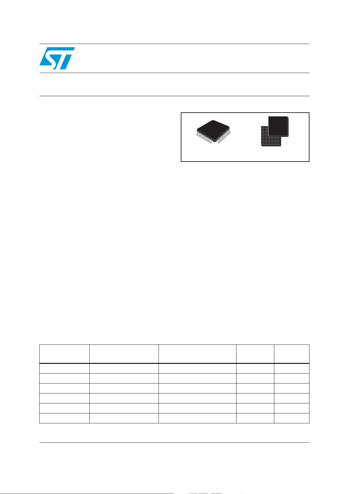
LQFP64
Evaluation kits
■ STA2058 module reference design (25x25mm)
■ Evaluation board hosting STA2058 module
■ SDK board (for application SW development)
Description
STA2058 is the high-sensitivity baseband of
TESEO GPS platform which include the STA5620
RF Front-End.
The embedded Flash memory enables the
equipment manufacturer to load the entire GPS
software (including tracking, acquisition,
navigation and data output) after customizing its
interfaces to his needs. A standard GPS library is
available from ST.
TESEO is the ideal solution for consumer,
handheld, PND (portable navigation), in vehicle
navigation and telematics systems.
LFBGA144
SBAS (WAAS and EGNOS) feature is also
supported.
Table 1. Device summary
Order code Package
STA2058 LQFP64 (10x10x1.4mm) No Tray No
STA2058TR LQFP64 (10x10x1.4mm) No Tape and reel No
STA2058EX LFBGA144 (10x10x1.7mm) Yes Tray No
STA2058EXTR LFBGA144 (10x10x1.7mm) Yes Tape and reel No
STA2058EXA LFBGA144 (10x10x1.7mm) Yes Tray Yes
STA2058EXATR LFBGA144 (10x10x1.7mm) Yes Tape and reel Yes
March 2009 Rev 3 1/20
For further information contact your local STMicroelectronics sales office.
(External Memory Interface)
EMI
Packing
Automotive
grade
www.st.com
20

Contents STA2058
Contents
1 Features summary . . . . . . . . . . . . . . . . . . . . . . . . . . . . . . . . . . . . . . . . . . 3
2 Pin description . . . . . . . . . . . . . . . . . . . . . . . . . . . . . . . . . . . . . . . . . . . . . 5
2.1 Logic symbol . . . . . . . . . . . . . . . . . . . . . . . . . . . . . . . . . . . . . . . . . . . . . . . 5
3 System block diagram . . . . . . . . . . . . . . . . . . . . . . . . . . . . . . . . . . . . . . . 6
3.1 Package LFBGA144 . . . . . . . . . . . . . . . . . . . . . . . . . . . . . . . . . . . . . . . . . . 8
3.2 Package LQFP64 . . . . . . . . . . . . . . . . . . . . . . . . . . . . . . . . . . . . . . . . . . . . 9
3.3 Power supply pins . . . . . . . . . . . . . . . . . . . . . . . . . . . . . . . . . . . . . . . . . . 10
4 Electrical characteristic . . . . . . . . . . . . . . . . . . . . . . . . . . . . . . . . . . . . . 11
4.1 DC electrical characteristic . . . . . . . . . . . . . . . . . . . . . . . . . . . . . . . . . . . . 11
4.2 AC electrical characteristics . . . . . . . . . . . . . . . . . . . . . . . . . . . . . . . . . . . 12
4.3 nRSTIN input filter characteristics . . . . . . . . . . . . . . . . . . . . . . . . . . . . . . 12
4.4 Flash electrical characteristics . . . . . . . . . . . . . . . . . . . . . . . . . . . . . . . . . 13
4.5 Oscillator electrical characteristics . . . . . . . . . . . . . . . . . . . . . . . . . . . . . . 14
4.6 ADC electrical characteristics . . . . . . . . . . . . . . . . . . . . . . . . . . . . . . . . . 14
4.7 PLL electrical characteristics . . . . . . . . . . . . . . . . . . . . . . . . . . . . . . . . . . 15
4.8 LVD electrical characteristics . . . . . . . . . . . . . . . . . . . . . . . . . . . . . . . . . . 15
4.9 GPS performances . . . . . . . . . . . . . . . . . . . . . . . . . . . . . . . . . . . . . . . . . . 16
5 Package information . . . . . . . . . . . . . . . . . . . . . . . . . . . . . . . . . . . . . . . . 17
6 Revision history . . . . . . . . . . . . . . . . . . . . . . . . . . . . . . . . . . . . . . . . . . . 19
2/20

STA2058 Features summary
1 Features summary
● ARM7TDMI 16/32 bit RISC CPU based host microcontroller running at a frequency up
to 66 MHz.
● Complete embedded memory system:
– Flash 256 Kbytes + 16 Kbytes (100 KB erasing/programming cycles)
– RAM 64 Kbytes.
● External memory interface provides glueless support for up to four banks of external
SRAM, Flash, ROM.
● High performance GPS engine (HPGPS).
● ST Proprietary CMOS (0.18 µm) Flash embedded technology.
● SBAS (WAAS and EGNOS) supported
● -40 °C to 85 °C operating temperature range.
● 144-pin LFBGA package and 64-pin LQFP package
● Power supply:
– 3.0 V to 3.6 V operating supply range for Input/Output periphery
– 3.0 V to 3.6 V operating supply range for A/D Converter reference
– 1.8 V operating supply range for core supply provided either by internal voltage
regulator (with external stabilization capacitor) or by external supply voltage.
● Reset and clock control unit able to provide low power modes (WAIT, SLOW, STOP,
STANDBY) and to generate the internal clock from the external reference through
integrated PLL.
● 48 programmable general purpose I/O, each pin programmable independently as
digital input or digital output; 40 (30 in LQFP64) are multiplexed with peripheral
functions; 16 can generate an interrupt on input level/transition.
● Real time clock module with 32 kHz low power oscillator and separate power supply to
continue running during standby mode.
● 16-bit Watchdog timer with 8 bits prescaler for system reliability and integrity.
● 2 CAN modules compliant with the CAN specification V2.0 part B (active) and bit rate
can be programmed up to 1 MBaud. One additional CAN at 1 Mbps (for STA2058 EM
SIP version)
● Four 16-bit programmable timers with 7 bit prescaler, up to two input capture/output
compare, one pulse counter function, one PWM channel with selectable frequency
each.
● 4 channels 12-bit sigma-delta analog to digital converter, single channel or multi
channel conversion modes, single-shot or continuous conversion modes, sample rate
1 kHz, conversion range 0-2.5 V .
● Three serial communication interfaces (UART) allow full duplex, asynchronous,
communications with external devices, independently programmable TX and RX baud
rates up to 625 Kbaud.
● One UART adapted to suit smart card interface needs, for asynchronous SC as defined
by ISO 7816-3. It includes SC clock generation.
● Two serial peripheral interfaces (SPI) allow full duplex, synchronous communications
with external devices, master or slave operation, max baud rate of 5.5 Mb/s. One SPI
may be used as multimedia card interface.
3/20

Features summary STA2058
● Two I
● Enhanced interrupt controller supports 32 interrupt vectors, independently maskable,
2
C Interfaces provide multi-master and slave functions, support normal and fast
2
I
C mode (400 KHz), 7/10 bit addressing modes. One I2C Interface is multiplexed with
one SPI, so either 2 x SPI + 1 x I
2
C or 1 x SPI + 2 x I2C may be used at a time.
with interrupt vector table for faster response and 16 priority levels, software
programmable for each source. Up to 2 maskable interrupts may be mapped on FIQ.
● Wakeup unit allows exiting from power down modes by detection of an event on two
external pins (one is active high and other is active low) or on internal real time clock
alarm.
● USB unit V1.1 compliant, software configurable endpoint setting, USB suspend/resume
support
● High level data link controller (HDLC) unit supports full duplex operating mode, NRZ,
NRZI, FM0 and MANCHESTER modes, and internal 8-bit baud rate generator.
4/20
STA2058 Pin description
2 Pin description
2.1 Logic symbol
Figure 1. STA2058 TESEO symbol
Power
Pads
Clock
& Reset
JTAG
Port
Debug
V18 (2)
V33 (7)
VSS (10)
AVSS
AVDD
V18BKP
GPSCLK
CK
CKOUT
RSTINn
JTDI
JTCK
JTMS
JTRSTn
JTDO
DBGRQS
BOOTEN
STA2058
TESEO
A[23:0]
D[15:0]
WEn.[1:0]
CSn.[3:0]
RDn
P0.[15:0]
P1.[15:0]
P2.[15:0]
(LFBGA144 Only)
nSTDBY_I
nSTDBY_O
RTCXTO
RTCXTI
WAKEUP
nWAKEUP
USBDN
USBDP
GPSDAT[1] LFBGA144 Only
GPSDAT[0]
EMI
Interface
LFBGA144
ONLY
GeneraI
Purpose I/O
RTC
& WKUP
Pads
USB Pads
5/20
System block diagram STA2058
3 System block diagram
Figure 2. STA2058 TESEO block diagram
1 DP
5 DP
3 DP
5 DP
4 AF
2 AF
4 AF
4 AF
ARM7TDMI
CPU
256K
Flash
64K
RAM
STC(JTAG)
VREG
RCCU
PLL
Interrupt
Contr.
12-bit A/D
Converter
TIMER0
TIMER1
TIMER2
TIMER3
EMI
APB
BRIDGE3
ARM7 Native BUS
APB
BRIDGE2
APB BUS
APB BUS
39 DP + 8 AF
HPGPS 16-ch.
correlator +
Emerald DSP
APB
BRIDGE1
I2C0
I2C1
SPI0
SPI1
UART0
UART1
UART2
3 DP
2 AF
2 AF
4 AF
4 AF
2 AF
2 AF
2 AF
RTC
2 DP
16 AF
2 AF
48 IO
OSCILL
Wakeup
WATCHDOG
Fully Prog.
I/O
6/20
UART3
[USB]
[CAN0]
[CAN1]
HDLC
2 AF
3 DP
2 AF
2 AF
3 AF

STA2058 System block diagram
Figure 3. New HPGPS 16-ch including Emerald DSP 16-bit
PRAM
EMERALD
INT
ARM
INT
pbus
pbus
ybus
xbus
4
APB bus
HPGPS_EME top
XBAR
ybus
xbus
APB
INT
3
YRAM
XRAM
Register
Interface
ISR
HPGPS
IP
AA
DA
RWA
CSA
AB
DB
RWB
CSB
Acquisition
Output Data
RAM A1
1023x32
RAM B1
1023x32
RAM A0
1023x32
RAM B0
1023x32
2046x32bit
RAM (*)
(*) Maximum memory size addressable by HPGPS. The real value depends on the device specs
7/20

System block diagram STA2058
3.1 Package LFBGA144
Table 2. Ball out for LFBGA144 package
ABCDEFGH J KL M
P0.10/
U1.RX/
1
U1.TX
VSS RDN
2
V33
3
P0.6/
4
S1.SCLK
A.19 WEn.1 WEn.0
5
P0.3/
S0.SSN/
6
I1.SDA
P0.2/
S0.SCLK/
7
I1.SCL
A.9 A.10 A.11 A.13
8
VSS18 V33 A.5 A.6 V33 D.15 D.10
9
A.8 V33
10
A.7 NC
11
A.12 A.4 A.3
12
P2.0/
CSn.0
P0.9/
U0.TX/
BOOT.0
P0.7/
S1.SSN
A.15 A.16 A.17 A.18 V33 V18 V18 V18BKP V18BKP VSSBKP nSTDBY_IN
P0.1/
S0.MOSI/
U3.RX
P2.1/
CSn.1
P0.11/
U1.TX/
BOOT.1
P0.12/
SCCLK
P0.8/
U0.RX/U0.
TX
P0.4/
S1.MISO
P1.15/
HTXD
P1.14/
HRXD/
I0.SDA
VSS
V33
P0.13/
U2.RX/
T2.OCMP
A
P0.14/
U2.TX/
T2.ICAPA
P0.5/
S1.MOSI
VSS V18 A.14 D.12 D.1 D.0
P1.13/
HCLK/
I0.SCL
P1.10/
USBCLK
P1.9/
PRN.11
P2.2/
CSn.2
P2.3/
CSn.3
P2.4/
A.20
P2.5/
A.21
P2.7/
A.23
P0.0/
S0.MISO/
U3.TX
VSS D.14 USBDN
A.2 D.13 USBDP
A.1
P2.6/
BOOTEN P2.12 P2.13 P2.15 JTDI NC
A.22
NC
P2.9/
CAN1_TX
P2.10/
CAN1_RX
T1.OCMPBD.8
NC V33IO-PLL
JTMS JTRSTn GPSCLK GPSDAT1
JTCK GPSDAT0 V33 VSSREG DBGRQS
WAKEUP_PAP0.15/
P1.12/
CANTX
P1.8/
PPS
P1.7/
VSSIO-
PLL
nSTDBY_
AVS S AV SS D.3 D.2
P1.0/
T3.OCMP
D.9
AIN.0
P1.5/
T1.ICAPB
D.5
P1.6/
T1.OCMPA
P1.4/
T1.ICAPA
D.7 D. 6
O
B/
T3.ICAPA/
T3.ICAPB/
VSS18 RSTINn
AIN.1
AIN.3
P2.8
VSS P2.11 JTDO CK CKOUT VSS VSS
VSS P2.14 NC RTCXTO RTCXTI
A.0 D.11
P1.11/
CANRX
V33REG_B
WAKEUP
NC AVDD
P1.1/
P1.3/
T3.OCMPA/
KP
D.4
AVD D
P1.2/
AIN.2
8/20

STA2058 System block diagram
3.2 Package LQFP64
Figure 4. LQFP64 package outline
P0.9/U0.TX/BOOT.0
P0.8/U0.RX/U0.TX
P0.7/S1.SSN
P0.6/S1.SCLK
P0.5/S1.MOSI
VSS
V18
VSS18
P0.4/S1.MISO
P0.3/S0.SSN/I1.SDA
P0.2/S0.SCLK/I1.SCL
P0.1/S0.MOSI/U3.RX
P0.0/S0.MISO/U3.TX
V33
VSS
P1.15/HTXD
P0.10/U1.RX/U1.TX
P0.11/U1.TX/BOOT.1
P0.12/SCCLK
U2.RX/T2.OCMPA
P0.13/
P0.14/U2.TX/T2.ICAPA
VSS
BOOTEN
VSS
JTDI
JTMS
JTCK
JTDO
nJTRST
GPSDAT
GPSCLK
V33
646362616059585756555453525150
1
2
3
4
5
6
7
8
9
10
11
12
13
14
15
16
171819202122232425262728293031
TESEO
LQFP64
49
48
P1.14/HRXD/I0.SDA
47
P1.13/HCLK/I0.SCL
46
P1.10/USBCLK
45
P1.9/PRN.11
44
VSS
43
P1.12/CANTX/USBDN
42
P1.11/CANRX/USBDP
41
P1.8/PPS
40
P1.7/T1.OCMPA
39
VSSIO-PLL
38
V33IO-PLL
37
P1.6/T1.OCMPB
36
P1.5/T1.ICAPB
35
P1.4/T1.ICAPA
34
P1.3/T3.ICAPB/AIN.3
33
P1.2/T3.OCMPA/AIN.2
32
CK
RTCXTI
VSSREG
V33REG_BKP
RTCXTO
nSTDBY_IN
P0.15/WAKEUP
V18
AVS S
AVD D
nRSTIN
VSS18
V18BKP
VSSBKP
P1.1/T3.ICAPA/AIN.1
P1.0/T3.OCMPB/AIN.0
Remapped for bkp supply
Double bond bw CAN & USB
Pads
9/20

System block diagram STA2058
3.3 Power supply pins
Table 3. Power supply pins
Symbol I/O Function LQFP 64 LFBGA144
V
V
SS
V
33IO-PLL
V
SSIO-PLL
V
33REG_B
KP
V
SSREG
V
18
V
SS18
V
18BKP
33
- Digital supply voltage for I/O circuitry (3.3 Volt) 9, 51
- Digital ground for I/O circuitry
Digital supply voltage for I/O circuitry and for PLL
reference (3.3V)
4, 8, 44,
50, 59
38 H12
D2,A3,K3,F6,B9
, E9,B10
D1,A2,F4,L4,M
4, F5, D7,E10
- Digital ground for I/O circuitry and for PLL reference 39 H11
Digital supply voltage for backup block I/O circuitry
and for ballast I/O (3.3V)
17 M2
- Digital ground for ballast I/O 18 L3
Digital supply voltage for core circuitry (1.8 Volt):
when using the internal voltage regulator, this pin
shall not be driven by an external voltage supply, but
-
a capacitance of at least 10μF (tantalum, low series
27, 58 G6, H6,E7
resistance) + 33nF (ceramic) shall be connected
between these pins and V
to guarantee on-chip
SS18
voltage stability.
- Digital Ground for core circuitry 28, 57 A9,L7
Digital supply voltage for backup block (RTC,
oscillator, Wake-up controller - 1.8 Volt): when using
the internal voltage regulator, this pin shall not be
-
driven by an external voltage supply, but a
26 J6,K6
capacitance of at least 1μF shall be connected
between this pin and V
to guarantee on-chip
SSBKP
voltage stability.
Note: V
V
SSBKP
AV
DD
AV
SS
and V
33
All V
SS
care of noise filtering, especially on AV
- Digital Ground for backup logic 25 L6
- Analog supply voltage for the A/D converter 29 M9, M11
- Analog supply Ground for the A/D converter 30 J8,K8
are all internally connected. Same for VSS and V
, V
SSBKP
, AV
pins must be tied together to the common ground plane, taking
SS
SS
, V
SS18
33IO-PLL
10/20
SSIO-PLL
.

STA2058 Electrical characteristic
4 Electrical characteristic
4.1 DC electrical characteristic
V33 = 3.3 V ± 10 %, TA = -40 / 85 °C unless otherwise specified.
Table 4. DC electrical characteristic
Symbol Parameter Test conditions
Val ue
Min. Typ. Max. Unit
V
V
R
R
V
IH
V
IL
HYS
OH
V
OL
WPU
WPD
Input high level CMOS With or w/o hysteresis 0.7V
33
Input high level P0.15 (WAKEUP) only 1.8 V
Input low level CMOS With or w/o hysteresis 0.3V
33
Input low level P0.15 (WAKEUP) only 0.7 V
Input hysteresis CMOS
Schmitt trigger
Input hysteresis
Schmitt trigger
Output high level
high current pins
Output high level
standard current pins
Output low level
standard current pins
P0.15 (WAKEUP) only 0.3 0.5 V
Push Pull, I
Push Pull, I
Push Pull, I
Push Pull, I
= 8mA V33-0.8
OH
= 4mA V33-0.8
OH
= 8mA 0.4 V
OH
= 4mA 0.4 V
OH
Weak pull-up resistor Measured at 0.5V
Weak pull-down resistor Measured at 0.5V
33
33
0.4 0.8 1.2 V
100 kΩ
100 kΩ
V
V
11/20

Electrical characteristic STA2058
4.2 AC electrical characteristics
Table 5. AC electrical characteristics
V
= 3.3 V ± 10 %, TA = 27 °C unless otherwise specified.
33
Val u e
Symbol Mode System clock
Unit
Min. Typ. Max.
I
DDRUN
I
DDWFI
I
DDLP
I
DDSTP
I
DDSB1
I
DDSB0
RUN mode 33 MHz system clock 60 mA
WFI mode 1 MHz system clock 5 mA
LPWFI mode 32 kHz system clock 300 µA
STOP mode Main VReg off, Flash in power-down 200 µA
STANDBY_1 mode LP VReg and 32kHz Osc on 15 30 µA
STANDBY_0 mode LP VReg, LVD, 32kHz Osc bypassed 3 10 µA
Note: IDDRUN is the consumption in applications exploiting the full performances of the core. A
typical GPS application would run at 33MHz, at the maximum frequency (66MHz) the power
consumption is IDDRUN = 150 mA (typ).
In WFI mode the VReg and Flash are ON to guarantees the minimum interrupt response
time.
Table 6. AC electrical characteristics
Symbol Mode System clock
V
= 3.3 V ± 10%, TA = -40 / 85 °C unless otherwise specified.
33
Val u e
Unit
Min. Typ. Max.
F
F
CPU
MAX
CPU max frequency Executing from RAM or EMI 66 MHz
Flash max frequency Executing from Flash 60 MHz
4.3 nRSTIN input filter characteristics
V
= 3.3 V ± 10 %, TA = -40 / 85 °C unless otherwise specified.
33
Table 7. nRSTIN input filter characteristics
Symbol Mode System clock
t
FR
t
NFR
Val ue
Min. Typ. Max.
nRSTIN input filtered pulse 100 ns
nRSTIN input not filtered pulse 1.2 µs
Unit
12/20

STA2058 Electrical characteristic
4.4 Flash electrical characteristics
V
= 3.3 ± 10%, TA = -40 / 85 °C unless otherwise specified.
33
Table 8. Flash program/erase characteristics 1
Val ue
Symbol Parameter Test conditions
t
t
PDW
t
PB0
t
PB1
t
t
t
t
t
RPD
t
PSL
t
ESL
Word program 40 µs
PW
Double word program 60 µs
Bank 0 program (256K) Double word program 1.6 2.1 4.3 s
Bank 1 program (16K) Double word program 130 170 300 ms
Sector erase (64K)
ES
Sector erase (8K)
ES
Bank 0 erase (256K)
ES
Bank 1 erase (16K)
ES
Not preprogrammed
Preprogrammed
Not preprogrammed
Preprogrammed
Not preprogrammed
Preprogrammed
Not preprogrammed
Preprogrammed
Recovery from power-down 20 µs
Program suspend latency 10 µs
Erase suspend latency 300 µs
Typ Ma x (C
2.3
1.9
0.7
0.6
8.0
6.6
0.9
0.8
4.0
3.3
1.1
1.0
13.7
11.2
1.5
1.3
)Max (C
0
4.9
4.1
1.36
1.26
17.2
14.0
1.87
1.66
max
Unit
)
s
s
s
s
Note: C0: TA = 85 °C after 0 cycles
C
: TA = 85 °C after max number of cycles
max
Table 9. Flash program/erase characteristics 2
Symbol Parameter Conditions
t
ESR
Endurance
Endurance (Bank1 sectors)
Data retention
Erase suspend rate
Min time from erase
resume to next erase
suspend
Val ue
Min Typ Max
10
100
20
20
Unit
Kcycles
Kcycles
Ye a r s
ms
13/20

Electrical characteristic STA2058
4.5 Oscillator electrical characteristics
V
= 3.3 ± 10 %, TA = -40 / 85 °C unless otherwise specified.
33
Figure 5. Crystal oscillator and resonator
DEVICE DEVICE
RTCXTI
R
C
L
Table 10. Oscillator electrical characteristics
RTCXTO
S
C
L
Symbol Parameter Test conditions
g
t
STUP
Oscillator transconductance 8 μA/V
m
Oscillator startup time Stable V
DD
4.6 ADC electrical characteristics
V
= 3.3 ± 10%, A
33
Table 11. ADC electrical characteristics
= 3.3V ± 10%, TA = -40 / 85 °C unless otherwise specified.
VDD
RTCXTI
RTCXTO
Val u e
Min Typ Max
Unit
2.5 s
Val ue
Symbol Parameter Test conditions
Min Typ Max
RES Resolution
ΔV
F
Input voltage range 0 2.5 V
IN
Modulator oversampling
Mod
frequency
IBW Input bandwidth
N
Number of input channels 4 n
ch
Sinewave with ΔV
amplitude
IN
12 bits
2.1 MHz
F
/40
Mod
96
PBR Passband ripple 0.1 dB
SINAD S/N and distortion 56 63 dB
THD Total harmonic distortion 60 74 dB
14/20
Unit
kHz

STA2058 Electrical characteristic
Table 11. ADC electrical characteristics (continued)
Val ue
Symbol Parameter Test conditions
Min Typ Max
Unit
Z
C
I
ADC
I
STBY
Input impedance F
IN
Input capacitance 5 pF
IN
= 2 MHz 1 MΩ
Mod
Power consumption TA=27 °C 2.5 3.0 mA
Standby power consumption TA=27 °C 1 µA
4.7 PLL electrical characteristics
V
= 3.3 ± 10 %, V
33
Table 12. PLL electrical characteristics
33IOPLL
Symbol Parameter Test conditions
T
T
ΔT
T
PLL1
T
PLL2
T
PLL3
LOCK
LOCK
JITTER
PLL reference clock FREF_RANGE=0 1.5 3.0 MHz
PLL reference clock
PLL reference clock
PLL lock time
PLL lock time
PLL jitter (peak to peak)
= 3.3 ± 10 %, TA = -40 / 85 °C unless otherwise specified.
FREF_RANGE=1
MX[1:0]=’00’ or ‘01’
FREF_RANGE=1
MX[1:0]=’10’ or ‘11’
FREF_RANGE=0
Stable Input Clock
Stable V
FREF_RANGE=1
Stable Input Clock
Stable V
T
= 4 MHz, MX[1:0]=’11’
PLL
Global Output division=32
(Output Clock=2 MHz)
33IOPLL
33IOPLL
, V
, V
18
18
Val ue
Unit
Min Typ Max
3.0 8.25 MHz
3.0 6 MHz
300 µs
600 µs
0.7 2 ns
4.8 LVD electrical characteristics
V
= 3.3 ± 10 %, TA = -40 / 85 °C unless otherwise specified.
33
Table 13. LVD electrical characteristics
Symbol Parameter Test conditions
T
LV D
ΔVVLPREG - T
LVD Threshold Main and LP LVD’s 1.3 V
LV D
Main regulator off 50 mV
15/20
Val ue
Unit
Min Typ Max

Electrical characteristic STA2058
4.9 GPS performances
V
= 3.3 ± 10 %, TA = 27 °C, unless otherwise specified
33
Table 14. GPS performances
Symbol Parameter Test conditions
Val ue
Unit
Min Typ Max
Reacquisition
HOt start <2.5 s
TTFF
Warm start <34 s
Cold start <39 s
Accuracy Autonomous
Acquisition (Warm start)
Sensitivity
Tracking -159 dBm
50%, -130dBm, Fu 2ppm,
Tu ± 2 , P u 3 0k m
CEP 50%, 24hr static at 130dBm
With external LNA
<1 s
2m
-146 dBm
16/20

STA2058 Package information
5 Package information
In order to meet environmental requirements, ST offers these devices in different grades of
ECOPACK
®
packages, depending on their level of environmental compliance. ECOPACK
®
specifications, grade definitions and product status are available at: www.st.com.
ECOPACK
®
is an ST trademark.
Figure 6. LQFP64 mechanical data and package dimensions
DIM.
A 1.60 0.063
A1 0.05 0.15 0.002 0.006
A2 1.35 1.40 1.45 0.053 0.055 0.057
B 0.17 0.22 0.27
C 0.09 0.0035
D 11.80 12.00 12.20 0.464 0.472 0.4 80
D1 9.80 10.00 10.20 0.386 0.394 0.401
D3 7.5 0 0.295
e 0.50 0.0197
E 11.80 12.00 12.20 0.464 0.472 0.480
E1 9.80 10.00 10.20 0.386 0.394 0.401
E3 7.50 0.295
L 0.45 0.60 0.75 0.0177 0.0236 0.0 295
L1 1.00 0.0393
K 0˚ (min.), 3.5˚ (min.), 7˚(max.)
ccc 0.080 0.0031
mm inch
MIN. TYP. MAX. MIN. TYP. MAX.
0.0066 0. 0086 0.0 106
0.20
0.0079
OUTLINE AND
MECHANICAL DATA
LQFP64 (10 x 10 x 1.4mm)
D
D1
48
49
B
64
1
e
TQFP64
33
32
E3D3E1
17
16
E
L1
L
K
0.08mm
Seating Plane
A
A2
A1
ccc
B
C
0051434 F
17/20

Package information STA2058
Figure 7. LFBG144 mechanical data and package dimensions
DIM.
mm inch
MIN. TYP. MAX. MIN. TYP. MAX.
A 1.21 1.70 0.0476 0.0669
A1 0.21 0.0083
A2 1.12 0.0441
b 0.35 0.40 0.45 0.0138 0.0157 0.0177
D 9.85 10.0 10.15 0.3878 0.3937 0.3996
D1 8.80 0.3465
E 9.85 10.0 10.15 0.3878 0.3937 0.3996
E1 8.80 0.3465
e 0.80 0.0315
F 0.60 0.0236
ddd 0.10 0.0039
eee 0.15 0.0059
fff 0.08 0.0031
OUTLINE AND
MECHANICAL DATA
Body: 10 x 10 x 1.7mm
LFBGA144
Low Profile Fine Pitch Ball Grid Array
18/20
7163385 D

STA2058 Revision history
6 Revision history
Table 15. Document revision history
Date Revision Changes
23-Apr-2007 1 Initial release.
25-Jun-2007 2
19-Mar-2009 3
Added features summary, pin description, electrical characteristics
and packages information.
Updated Table 1: Device summary on page 1.
Updated ECOPACK description in Section 5: Package information on
page 17.
19/20

STA2058
Please Read Carefully:
Information in this document is provided solely in connection with ST products. STMicroelectronics NV and its subsidiaries (“ST”) reserve the
right to make changes, corrections, modifications or improvements, to this document, and the products and services described herein at any
time, without notice.
All ST products are sold pursuant to ST’s terms and conditions of sale.
Purchasers are solely responsible for the choice, selection and use of the ST products and services described herein, and ST assumes no
liability whatsoever relating to the choice, selection or use of the ST products and services described herein.
No license, express or implied, by estoppel or otherwise, to any intellectual property rights is granted under this document. If any part of this
document refers to any third party products or services it shall not be deemed a license grant by ST for the use of such third party products
or services, or any intellectual property contained therein or considered as a warranty covering the use in any manner whatsoever of such
third party products or services or any intellectual property contained therein.
UNLESS OTHERWISE SET FORTH IN ST’S TERMS AND CONDITIONS OF SALE ST DISCLAIMS ANY EXPRESS OR IMPLIED
WARRANTY WITH RESPECT TO THE USE AND/OR SALE OF ST PRODUCTS INCLUDING WITHOUT LIMITATION IMPLIED
WARRANTIES OF MERCHANTABILITY, FITNESS FOR A PARTICULAR PURPOSE (AND THEIR EQUIVALENTS UNDER THE LAWS
OF ANY JURISDICTION), OR INFRINGEMENT OF ANY PATENT, COPYRIGHT OR OTHER INTELLECTUAL PROPERTY RIGHT.
UNLESS EXPRESSLY APPROVED IN WRITING BY AN AUTHORIZED ST REPRESENTATIVE, ST PRODUCTS ARE NOT
RECOMMENDED, AUTHORIZED OR WARRANTED FOR USE IN MILITARY, AIR CRAFT, SPACE, LIFE SAVING, OR LIFE SUSTAINING
APPLICATIONS, NOR IN PRODUCTS OR SYSTEMS WHERE FAILURE OR MALFUNCTION MAY RESULT IN PERSONAL INJURY,
DEATH, OR SEVERE PROPERTY OR ENVIRONMENTAL DAMAGE. ST PRODUCTS WHICH ARE NOT SPECIFIED AS "AUTOMOTIVE
GRADE" MAY ONLY BE USED IN AUTOMOTIVE APPLICATIONS AT USER’S OWN RISK.
Resale of ST products with provisions different from the statements and/or technical features set forth in this document shall immediately void
any warranty granted by ST for the ST product or service described herein and shall not create or extend in any manner whatsoever, any
liability of ST.
ST and the ST logo are trademarks or registered trademarks of ST in various countries.
Information in this document supersedes and replaces all information previously supplied.
The ST logo is a registered trademark of STMicroelectronics. All other names are the property of their respective owners.
© 2009 STMicroelectronics - All rights reserved
STMicroelectronics group of companies
Australia - Belgium - Brazil - Canada - China - Czech Republic - Finland - France - Germany - Hong Kong - India - Israel - Italy - Japan -
Malaysia - Malta - Morocco - Singapore - Spain - Sweden - Switzerland - United Kingdom - United States of America
www.st.com
20/20
 Loading...