

DSP/MCU system for CD-DA, CD-CA, CD-ROM player
Features
■ CD-R, CD-RW playback
■ Audio decoding (MP3,WMA,AAC)
■ CLV (1x, 2x, 4x) and CAV mode (6x)
■ On-chip USB-OTG host full speed
■ 3.3 V ±5 % operating supply range for I/O
■ 1.8 V ±5 % operating supply range for logic
■ IDLE, WFI and STOP modes
■ Power on reset / Brownout controller
■ 33.8688 MHz external quartz/resonator
■ Operating temperature range: -40 °C to +85 °C
Embedded ARM7TDMI microcontroller
32 bit MCU with 3-stage pipeline @ 67 MHz
■
■ 384 KB internal ROM (4 Mb on package RAM
for development version) and 128 KB RAM
2
■ I
C master/slave (400 kHz) + 1 CRQ line
■ Two high-speed UART full-duplex
■ Two buffered SPI master/slave interface
Analog Front-end part
■ A, B, C, D, E, F voltage inputs
■ Automatic gain and offset control
■ ALPC circuit with integrated Power MOS
■ 8 bit 2 channels general purpose ADC
Digital servo
■ Automatic fine gain/balance/offset adjustment
for tracking and focus
■ Embedded 16 bit servo DSP (33.8688 MHz)
■
PDM controls for focus, tracking, spindle, sledge
■ Embedded stepping sledge motor controller
■ CLV & CAV spindle control
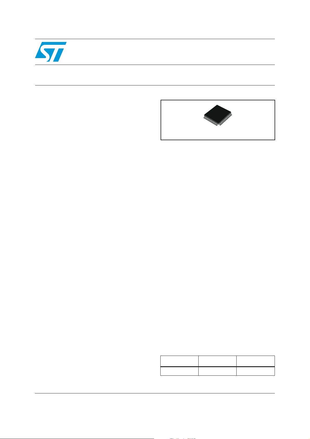
STA1052
Data Brief
LQFP144 (20x20x1.4 mm)
Acquisition
■ Full range adjustment-free digital PLL
■ EFM demodulation and synchronization
■ Q subcode and CD text decoder
Error correction
■ CIRC, capable of dual C1, quad C2 erasure
■ RSPC capable of C3 corrections
■ Jitter absorbing capacity ±24 frames (CLV)
Shock-proof controller
■ Up to 64 Mbit external SDRAM interface
■ 8/16 bit data bus interface
■ ADPCM (4:1) lossy compression for extended
shock proof capability
Audio features
■ Two I
■ SPDIF transmitter (IEC958) and receiver
■ Sample-rate conversion from 8 kHz - 48 kHz
■ Digital equalizer for bass/treble control
■ Built-in stereo DAC
Development environment
■ 5 pin JTAG port (IEEE 1149.1 standard)
Table 1. Device summary
2
S transmitters and one I2S receiver
input to 44.1 kHz output
Order code Package Packing
STA1052S1 LQFP144 Tray
March 2008 Rev 1 1/14
For further information contact your local STMicroelectronics sales office.
www.st.com
14

Contents STA1052
Contents
1 Description . . . . . . . . . . . . . . . . . . . . . . . . . . . . . . . . . . . . . . . . . . . . . . . . . 3
2 System block diagram . . . . . . . . . . . . . . . . . . . . . . . . . . . . . . . . . . . . . . . 4
3 Pin description . . . . . . . . . . . . . . . . . . . . . . . . . . . . . . . . . . . . . . . . . . . . . 5
3.1 Pin connection . . . . . . . . . . . . . . . . . . . . . . . . . . . . . . . . . . . . . . . . . . . . . . 5
3.2 Pin function description . . . . . . . . . . . . . . . . . . . . . . . . . . . . . . . . . . . . . . . 6
4 Package information . . . . . . . . . . . . . . . . . . . . . . . . . . . . . . . . . . . . . . . . 12
5 Revision history . . . . . . . . . . . . . . . . . . . . . . . . . . . . . . . . . . . . . . . . . . . 13
2/14

STA1052 Description
1 Description
The STA1052 is a single chip device which performs all functions related to read back of
optical disk: servo control operations, reading optical disc decoding the High frequency
signals, EFM decoding, error correction, software decoding of MP3 and WMA encoded
audio, sample rate conversion, managing file system, serial transfer of audio/program
through I
It also performs software decoding of MP3, AAC and WMA encoded audio from USB or
SD card™ memory supports.
Commands can be exchanged with the Host MCU either via one I
STA1052 chip comes along a broad software suite that comprehends different types of
compressed audio files, File System Management, Play Lists.
The key Media and File Types supported are briefly reported below:
● Ability to play any USB/SD card compatible solid state memory media
● MPEG1-Layer 2 compressed audio files
● Playback of MP3 compressed audio files (all bit rates and VBR)
● Playback of lower bit rate MPEG2 layer 3 files and MPEG-2.5 extension
● Playback of WMA version 9 compressed audio files
● Playback of iTunes AAC compressed audio files
● Sample rate converter for recorded sampling rates other than 44.1kHz
● Support FAT16/FAT32 file systems
● Support ISO9660 and Joliet file systems
2
S/SPDIF, direct playback of audio through in-built audio DAC.
2
C port or two SPI ports.
The software can manage the following File Information: folder and file names.
ID3 tag information - as per versions 1.0-1.1, 2.0 - 2.4- is reported. Further parameters
made available by ST software are: File type (i.e. .mp3, .wav, .wma, .cda, .aac), Bit rate,
entire file path for current track and track elapsed time.
STA1052 software provides the essential Navigation Commands: Previous/Next , Fast
forward/Rewind, Jump to any file, Scan, Pause. All these commands can be programmed
and configured via Command Protocol Interface.
Two different types of Playlists are supported: Playlists with .pls extension, Playlists with
.m3u extension.
Robust software architecture provides an efficient error handling and related messaging.
ST developed a software architecture that allows the patching of a few parts of software
resident in ROM. Software patches are loaded into a very inexpensive serial Flash which
provides the capability to patch up to 40 KByte of ROM software.
Software build (patching) upgrade from media USB and SD card and from host MCU onto
serial Flash is supported.
STA1052 is intended for use in automotive entertainment system.
3/14

System block diagram STA1052
2 System block diagram
Figure 1 provides the complete system block diagram, where the ARM sub-system is
represented as a hierarchical block.
Figure 1. STA1052 block diagram
SPDIF-SONYLSI-I2S
fade/
mute/
deemph
master clock
Application interfaceOutput interface
Obs/Debug
ARM Subsystem
External
Focus Actuator
Track Actuator
Ext
Interrupt
Mem
Sled Motor
Spindle Motor
SDRAM Interface
ADPCM
De-
Decoder
ADPCM
Encoder
Org
Frame
+
RSPC
Scram
CLV
buffer
Reed-Solomon
Cross Interleaving
AHB
ITF
DSP
1.7Kx32 PRAM
256x16 XRAM
256x16 YRAM
TrackCount
A+C B+D E F
JumpSpeed
stepper
PDM/
SLED Loop filter
Track Loop filter
Focus Loop filter
TE
FE
defect
Spindle Motor Feedback (CAV)
Sub code
Digital PLL
Sync protection &
decoder
EFM demodulator
+
digital
equalizer
AUX ADC
Laser
control
LD
MD
4/14
ADC1
ADC2
ABCDE
OFFSET GAIN ADC
I/V
+
RATE
DECIM.
F
E
B+D
A+C
DAC
filter
ANALOG
AUDIO L/R out
PLL
Quartz/
Ceramic
F
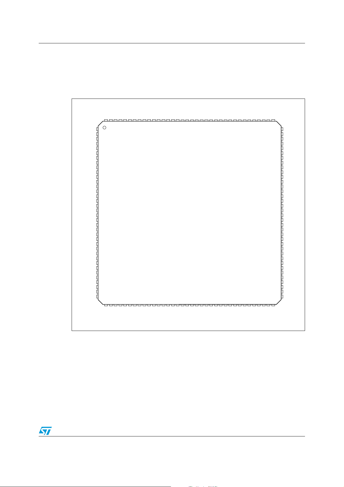
STA1052 Pin description
3 Pin description
3.1 Pin connection
Figure 2. LQFP144 pin configuration (top view)
DRD10
DRD11
GPB11
GPB10
GPB9
DRD12
DRD13
DRD14
DRD15
VDD3_Core1
VSS
DRCLK
DRCLKE
DRRAS
DRCAS
DRWR
DRA0
DRA1
DRA2
DRA3
DRA4
VDD3
VSS
VDD
DRA5
DRA6
DRA7
DRA8
DRA9
DRA10
DRA11
DRBA0
DRBA1
JTRST
JTCK
NC
DRD9
DRD8
GPB12
GPB13
GPB14
GPB15
DRD7
DRD6
DRD5
VDD
VDD3
DRD4
DRD3
DRD2
DRD1
DRD0
PLL_VSS18P
PLL_VDDA33P
PLL_XTI
PLL_XTO
PLL_VDDA18P
PLL_VDD18P
FE_VSSA33S
FE_A
FE_C
FE_B
FE_D
FE_E
FE_F
FE_VDDA33S
FE_VDDPAD1
FE_ADCIN1
FE_ADCIN2
FE_VREF_ADC
FE_VREF
VSS
1
2
3
4
5
6
7
8
9
10
12
13
14
15
16
17
18
19
20
21
22
23
24
25
26
27
28
29
30
31
32
33
34
35
36
37 38 39 40
138139140141
137142143144
41 42 43 44 45
135134 133132
136
461147 48 49 50 51
130
131 129 128127 126125
54 55 56 57 58 59
52 53
122
124
123 121 120119 118117
60 61
115
116
62 63 64 65 66 67
114
112
113
68 69 70
111110 109
71
108
OUTR
ADAC_REF1
107
VCM
106
ADAC_REF2
105
OUTL
104
103
ADAC_VDDA
102
ADAC_VSSA
101
VSS
100
VDD3
99
JTMS
98
JTDO
97
JTDI
96
GPB7
95
GPB6
94
VDD
93
GPB8
92
GPB5
91
GPB4
90
GPB3
89
GPB2
88
GPB1
87
VDD3_Core2
86
VSS
85
GPB0
84
GPA8
83
GPA7
82
GPA6
81
GPA5
80
GPA4
79
GPA13
78
GPA3
77
GPA2
76
GPA1
75
NC
74
NC
73
NC
72
FE_CEXT
FE_REXT
FE_VDDA33R
FE_MD_LAS
FE_VSSA33R
FE_CAP_LAS
FE_LD_LAS
1. NC defines not connected pins.
FE_LD1_LAS
FE_VDDA33T
FE_VDDPAD2
FE_TESTP
FE_TESTN
FE_VSSA33T
FE_VSSA18AD
FE_VDDA18AD
VSS
TESTEN
RESETN
FFSR
SPDL
REFFSR
SLED1
SLED2
VDD
VSS
VDD3
TFSR
CAV
LRCK
GPA9
GPA10
GPA11
GPA12
SDO
BCLK
GPA0
AC00563
5/14

Pin description STA1052
3.2 Pin function description
This pin list contains the definition and description of all pins.
Tab l e 2 gives pin list for LQFP144.
Table 2. Pin List
N° Name Description Pin type LQFP144
1 GPC9(DRD9) GPIO PC9 (SDRAM data 9) bidir, 3.3V , 4 mA 1
2 GPC8(DRD8) GPIO PC8 (SDRAM data 8) bidir, 3.3 V, 4 mA 2
3 GPB12 GPIO PB12(BSPI1_SS)
4 GPB13 GPIO PB13 (BSPI1_MISO)
bidir, 3.3 V, 2 mA,
PU (default off)
bidir, 3.3 V, 2 mA,
PU (default off)
3
4
5 GPB14 GPIO PB14 (BSPI1_MOSI)
6 GPB15 GPIO PB15 (BSPI1_SCK)
7 GPC7(DRD7) GPIO PC7 (SDRAM data 7) bidir, 3.3 V, 4 mA 7
8 GPC6(DRD6) GPIO PC6 (SDRAM data 6) bidir, 3.3 V, 4 mA 8
9 GPC5(DRD5) GPIO PC5 (SDRAM data 5) bidir, 3.3 V, 4 mA 9
10 VDD Core VDD1.8 V VDD 10
11 VSS Digital pad ring VSS ground VSS 11
12 VDD3 Digital pad ring VDD3 3.3 V VDD3 12
13 GPC4(DRD4) GPIO PC4 (SDRAM data 4) bidir, 3.3 V, 4 mA 13
14 GPC3(DRD3) GPIO PC3 (SDRAM data 3) bidir, 3.3 V, 4 mA 14
GPC2(DRD2/
15
SFLASH_MISO)
GPC1(DRD1/
16
SFLASH_MOSI)
GPC0(DRD0/
17
SFLASH_SCK)
18 PLL_VSS18P PLL digital & analog ground VSS 18
19 PLL_VDDA33P PLL 3.3 analog power supply VDD 19
GPIO PC2 (SDRAM data 2 or serial
flash master in/slave out)
GPIO PC1 (SDRAM Data 1 or serial
flash master out/slave in)
GPIO PC0 (SDRAM data 0 or serial
Flash clock)
bidir, 3.3 V, 2 mA,
PU (default off)
bidir, 3.3 V, 2 mA,
PU (default off)
bidir, 3.3 V, 4 mA 15
bidir, 3.3 V, 4 mA 16
bidir, 3.3 V, 4 mA 17
5
6
20 PLL_XTI Crystal input analog in 20
21 PLL_XTO Crystal output analog out 21
22 PLL_VDDA18P PLL 1.8V analog power supply VDD 22
23 PLL_VDD18P PLL 1.8V digital power supply VDD 23
24 FE_VSSA33S Ground for servo channels VSS 24
25 FE_A OPU A input analog in 25
26 FE_C OPU C input analog in 26
6/14

STA1052 Pin description
Table 2. Pin List (continued)
N° Name Description Pin type LQFP144
27 FE_B OPU B input analog in 27
28 FE_D OPU D input analog in 28
29 FE_E OPU E input analog in 29
30 FE_F OPU F input analog in 30
3.3 V analog for servo channels/ 3.3 V
31 FE_VDDA33S
32 FE_VDDPAD1 3.3V for AFE pad ring VDD 32
33 FE_ADCIN1 General purpose ADC input 1 analog in 33
34 FE_ADCIN2 General purpose ADC input 2 analog in 34
for AFE pad ring (decoupling cap to
Vssa)
VDD 31
35 FE_VREF_ADC
36 FE_VREF
37 FE_VDDA33R Analog 3.3 V for bandgap VDD 37
38 FE_CEXT External cap for bandgap (1 nF) analog 38
39 FE_REXT External res for bandgap (25 kOhm) analog 39
40 FE_VSSA33R Analog ground bandgap Vss 40
41 FE_MD_LAS Laser driver input from monitor diode analog in 41
42 FE_CAP_LAS Laser driver compensation cap (30 nF) analog 42
43 FE_LD_LAS First laser driver output analog out 43
44 FE_LD1_LAS Second laser driver output analog out 44
45 FE_VDDPAD2 3.3 V for AFE pad ring VDD 45
46 FE_VDDA33T Analog 3.3 V for test buffer VDD 46
47 FE_TESTP Test buffer positive output analog out 47
48 FE_TESTN Test buffer negative output analog out 48
49 FE_VSSA33T Analog ground test buffer VSS 49
50 FE_VDDA18AD Analog 1.8 V ADC VDD 50
51 FE_VSSA18AD Analog ground ADC VSS 51
52 VSS Core VSS ground VSS 52
General purpose ADC Vtop reference
output
External Vref pickup (decoupling cap 1
nF)
analog out 35
analog out 36
53 RESETN Hardware reset input (pull-up) in, schmitt, 3.3 V 53
54 TESTEN Test enable signal (active low) in, 3.3V 54
55 FFSR
56 REFFSR
Focusing actuator control signal output PDM
Clock (50% duty cycle) for actuator
PDM reference
7/14
Out, 3.3 V, 4 mA 55
Out, 3.3 V, 2 mA 56

Pin description STA1052
Table 2. Pin List (continued)
N° Name Description Pin type LQFP144
57 SPDL
58 SLED1
59 SLED2
60 VDD Core VDD 1.8 V VDD 60
61 VSS Digital pad ring VSS ground VSS 61
62 VDD3 Digital pad ring VDD3 3.3 V VDD3 62
63 TFSR
64 CAV CAV feedback input in, 3.3 V 64
65 LRCK Serial L/R clock bidir, 3.3 V, 2 mA 65
66 GPA9 GPA9 (I2S1_Tx_SCK (SCK1))
67 GPA10 GPA10 (I2S1_Tx_WCK (SC12))
68 GPA11 GPA11 (I2S1_Tx_SDO (STD1))
69 GPA12 GPA12 (I2S1_ref_CK)
Spindle motor control signal output PDM
SLED motor control signal output1
(stepping/DC) - PDM
SLED motor control signal output2
(stepping) -PDM
Tracking actuator control signal output PDM
Out, 3.3 V, 2 mA 57
Out, 3.3 V, 2 mA 58
Out, 3.3 V, 2 mA 59
Out, 3.3 V, 4 mA 63
bidir, 3.3 V, 2 mA,
PU (default off)
bidir, 3.3 V, 2 mA,
PU (default off)
bidir, 3.3 V, mA,
PU (default off)
bidir, 3.3 V, 2 mA,
PU (default off)
66
67
68
69
70 SDO/SPDIF Serial bit data or SPDIF Digital output bidir, 3.3 V, 2 mA 70
71 BCLK Serial bit clock bidir, 3.3 V, 2 mA 71
72 GPA0 (EINT0)
- NC Not connected 73
- NC Not connected 74
- NC Not connected 75
73 GPA1 (EINT1)
74 GPA2 (EINT2)
75 GPA3 (EINT3)
76 GPA13 GPIO PA13 (SPDIF Rx)
77 GPA4 (EINT4) GPIO PA4 (external interrupt 4)
78 GPA5 (EINT5) GPIO PA5 (external interrupt 5)
GPIO PA0 (external interrupt 0/timer 0
output 0)
GPIO PA1 (external interrupt 1/timer 0
output 1)
GPIO PA2 (external interrupt 2/timer 1
output 0)
GPIO PA3 (external interrupt 3/timer 1
output1 )
bidir, 3.3 V, 2 mA,
PU (default off)
bidir, 3.3 V, 2 mA,
PU (default off)
bidir, 3.3 V, 2 mA,
PU (default off)
bidir, 3.3 V, 2 mA,
PU (default off)
bidir, 3.3 V, 2 mA,
PU (default off)
bidir, 3.3 V, 2 mA,
PU (default off)
bidir, 3.3 , 2 mA,
PU (default off)
72
76
77
78
79
80
81
8/14

STA1052 Pin description
Table 2. Pin List (continued)
N° Name Description Pin type LQFP144
79 GPA6 (EINT6) GPIO PA6 (external interrupt 6)
80 GPA7 (EINT7) GPIO PA7 (external interrupt 7)
81 GPA8 (EINT8) GPIO PA8 (external interrupt 8)
GPB0/SFLASH_SS
82
(EINT9)
GPIO PB0 or serial Flash slave select
(external interrupt 9)
bidir, 3.3 V, 2 mA,
PU (default off)
bidir, 3.3 V, 2 mA,
PU (default off)
bidir, 3.3 V, 2 mA,
PU (default off)
bidir, 3.3 V, 2 mA,
PU (default off)
82
83
84
85
83 VSS Digital pad ring VSS ground Vss 86
84 VDD3_Core2 Digital pad ring VDD3 3.3 V VDD3 87
GPB1/I2C_CRQ
85
(EINT10)
GPB2/I2C_SCL
86
(EINT11)
GPB3/I2C_SDA
87
(EINT12)
88 GPB4/SCI0TX
GPB5/SCI0RX
89
(EINT13)
90 GPB8/C2PO/USBCK
GPIO PB1 or I2C CRQ line
(external interrupt 10)
GPIO PB2 or I2C I/F clock
(external interrupt 11)
GPIO PB3 or I2C I/F data
(external interrupt 12)
GPIO PB4 or serial interface 0 TX or
EXTCK_OIF
GPIO PB5 or serial interface 0 RX
(external interrupt 13)
GPIO PB8 or C2PO (EIAJ CP-340) or
USB clock line (48 MHz)
bidir, 5 V tol, 2 mA(sink) 88
bidir, 5 V tol, 2 mA(sink) 89
bidir, 5 V tol, 2 mA(sink) 90
bidir, 3.3 V, 2mA,
PU (default off)
bidir, 3.3V, 2mA,
PU (default off)
bidir, 3.3V, 2mA,
PU (default off)
91
92
93
91 VDD Core VDD 1.8 V VDD 94
92 GPB6/SCI1TX/USBDM
GPIO PB6 or serial interface 1 TX or
USB D- line
bidir, 3.3 V, 2 mA, PU
(default off)
USB pad (Full / Low
(1)
95
speed )
bidir, 3.3 V, 2 mA, PU
(default off)
(1)
USB pad (Full / Low
speed )
96
GPB7/SCI1RX/USBDP
93
(EINT14)
GPIO PB7 or serial interface 1 RX or
USB D+ line
(external interrupt 14)
94 JTDI JTAG test data input in, 3.3V 97
95 JTDO JTAG test data output out, 3.3 V, 2 mA 98
96 JTMS JTAG test mode select input in, 3.3 V 99
97 VDD3 Digital pad ring VDD3 3.3 V VDD3 100
98 VSS Digital pad ring VSS ground Vss 101
99 ADAC_VSSA Audio DAC ground VSSDAC 102
100 ADAC_VDDA Audio DAC supply 3.3 V VDDDAC 103
101 OUTL Left channel analog output analog out 104
102 ADAC_REF2 Audio DAC VLO (GND) analog in 105
9/14

Pin description STA1052
Table 2. Pin List (continued)
N° Name Description Pin type LQFP144
103 VCM
104 ADAC_REF1 Audio DAC VHI (3.3 V) analog in 107
105 OUTR Right channel analog output analog out 108
- NC Not Connected 109
106 JTCK JTAG test clock input in, 3.3 V 110
107 JTRST JTAG test reset input in, schmitt, 3.3 V 111
108 DRBA1 SDRAM bank sel address 1 out, 3.3 V, 4 mA 112
109 DRBA0/CFG4
110 DRA11/CFG3
111 DRA10/CFG2
112 DRA9/CFG1
113 DRA8/CFG0
114 DRA7 SDRAM address 7 out, 3.3 V, 4 mA 118
Common Mode input for audio DAC
(1.65 V)
SDRAM bank sel address 0 and
configuration bit 4
(latched at reset)
SDRAM address 11 and configuration
bit 3
(latched at reset)
SDRAM Address 10 and configuration
bit 2
(latched at reset)
SDRAM Address 9 and configuration bit
1
(latched at reset)
SDRAM Address 8 and configuration bit
0
(latched at reset)
analog in 106
bidir, 3.3 V, 4 mA 113
bidir, 3.3V, 4mA 114
bidir, 3.3 V, 4 mA 115
bidir, 3.3 V, 4 mA 116
bidir, 3.3 V, 4 mA 117
115 DRA6 SDRAM address 6 out, 3.3 V, 4 mA 119
116 DRA5 SDRAM address 5 out, 3.3 V, 4 mA 120
117 VDD Core VDD 1.8 V VDD 121
118 VSS Digital pad ring VSS ground VSS 122
119 VDD3 Digital pad ring VDD3 3.3 V VDD3 123
120 DRA4 SDRAM address 4 out, 3.3 V, 4 mA 124
121 DRA3 SDRAM address 3 out, 3.3 V, 4 mA 125
122 DRA2 SDRAM address 2 out, 3.3 V, 4 mA 126
123 DRA1 SDRAM address 1 out, 3.3 V, 4 mA 127
124 DRA0 SDRAM address 0 out, 3.3 V, 4 mA 128
125 DRWR SDRAM write control out, 3.3 V, 4 mA 129
126 DRCAS SDRAM col address sel out, 3.3 V, 4 mA 130
127 DRRAS SDRAM row address sel out, 3.3 V, 4 mA 131
128 DRCLKE SDRAM CLK enable out, 3.3 V, 4 mA 132
129 DRCLK SDRAM CLK out, 3.3 V, 4 mA 133
10/14

STA1052 Pin description
Table 2. Pin List (continued)
N° Name Description Pin type LQFP144
130 VSS Digital pad ring VSS ground VSS 134
131 VDD3_Core1 Digital pad ring VDD3 3.3 V VDD3 135
132 GPC15 (DRD15) GPIO PC15 (SDRAM Data 15) bidir, 3.3 V, 4 mA 136
133 GPC14 (DRD14) GPIO PC14 (SDRAM Data 14) bidir, 3.3 V, 4 mA 137
134 GPC13 (DRD13) GPIO PC13 (SDRAM Data 13) bidir, 3.3 V, 4 mA 138
135 GPC12 (DRD12) GPIO PC12 (SDRAM Data 12) bidir, 3.3 V, 4 mA 139
136 GPB9 GPB9 (I2S1_Rx_SCK (SC10))
137 GPB10 GPB10 (I2S1_Rx_WCK (SC11))
bidir, 3.3 V, 2 mA,
PU (default off)
bidir, 3.3V, 2mA,
PU (default off)
140
141
138 GPB11 GPB11 (I2S1_Rx_SDI (SRD1))
139 GPC11 (DRD11) GPIO PC11 (SDRAM Data 11) bidir, 3.3 V, 4 mA 143
140 GPC10 (DRD10) GPIO PC10 (SDRAM Data 10) bidir, 3.3V , 4 mA 144
1. The specifications in USB mode are as per USB specifications for low and full speed interface.
bidir, 3.3 V, 2 mA,
PU (default off)
142
11/14

Package information STA1052
4 Package information
In order to meet environmental requirements, ST (also) offers these devices in ECOPACK®
packages. ECOPACK
®
packages are lead-free. The category of second Level Interconnect
is marked on the package and on the inner box label, in compliance with JEDEC Standard
JESD97. The maximum ratings related to soldering conditions are also marked on the inner
box label.
ECOPACK is an ST trademark. ECOPACK specifications are available at: www.st.com.
Figure 3. LQFP144 (20x20x1.4mm) mechanical data and package dimensions
DIM.
A 1.600 0.0630
A1 0.050 0.150 0.0020 0.0059
A2 1.350 1.400 1.450 0.0531 0.0551 0.0571
b 0.170 0.220 0.270 0.0067 0.0087 0.0106
c 0.090 0.200 0.0035 0.0079
D 21.800 22.000 22.200 0.8583 0.8661 0.8740
D1 19.800 20.000 20.200 0.7795 0.7874 0.7953
D3 17.500 0.6890
E 21.800 22.000 22.200 0.8583 0.8661 0.8740
E1 19.800 20.000 20.200 0.7795 0.7874 0.7953
E3 17.500 0.6890
e 0.500 0.0197
L 0.450 0.600 0.750 0.0177 0.0236 0.0295
L1 1.000 0.0394
k 0˚(min.), 3.5˚ (typ.), 7˚( max.)
ccc 0.080 0.0031
mm inch
MIN. TYP. MAX. MIN. TYP. MAX.
OUTLINE AND
MECHANICAL DATA
LQFP144 (20x20x1.40mm)
Low profile plastic Quad Flat Package
Note 1: Exact shape of each corner is optional.
12/14
0099183 C

STA1052 Revision history
5 Revision history
Table 3. Document revision history
Date Revision Changes
12-Mar-2008 1 Initial release.
13/14

STA1052
Please Read Carefully:
Information in this document is provided solely in connection with ST products. STMicroelectronics NV and its subsidiaries (“ST”) reserve the
right to make changes, corrections, modifications or improvements, to this document, and the products and services described herein at any
time, without notice.
All ST products are sold pursuant to ST’s terms and conditions of sale.
Purchasers are solely responsible for the choice, selection and use of the ST products and services described herein, and ST assumes no
liability whatsoever relating to the choice, selection or use of the ST products and services described herein.
No license, express or implied, by estoppel or otherwise, to any intellectual property rights is granted under this document. If any part of this
document refers to any third party products or services it shall not be deemed a license grant by ST for the use of such third party products
or services, or any intellectual property contained therein or considered as a warranty covering the use in any manner whatsoever of such
third party products or services or any intellectual property contained therein.
UNLESS OTHERWISE SET FORTH IN ST’S TERMS AND CONDITIONS OF SALE ST DISCLAIMS ANY EXPRESS OR IMPLIED
WARRANTY WITH RESPECT TO THE USE AND/OR SALE OF ST PRODUCTS INCLUDING WITHOUT LIMITATION IMPLIED
WARRANTIES OF MERCHANTABILITY, FITNESS FOR A PARTICULAR PURPOSE (AND THEIR EQUIVALENTS UNDER THE LAWS
OF ANY JURISDICTION), OR INFRINGEMENT OF ANY PATENT, COPYRIGHT OR OTHER INTELLECTUAL PROPERTY RIGHT.
UNLESS EXPRESSLY APPROVED IN WRITING BY AN AUTHORIZED ST REPRESENTATIVE, ST PRODUCTS ARE NOT
RECOMMENDED, AUTHORIZED OR WARRANTED FOR USE IN MILITARY, AIR CRAFT, SPACE, LIFE SAVING, OR LIFE SUSTAINING
APPLICATIONS, NOR IN PRODUCTS OR SYSTEMS WHERE FAILURE OR MALFUNCTION MAY RESULT IN PERSONAL INJURY,
DEATH, OR SEVERE PROPERTY OR ENVIRONMENTAL DAMAGE. ST PRODUCTS WHICH ARE NOT SPECIFIED AS "AUTOMOTIVE
GRADE" MAY ONLY BE USED IN AUTOMOTIVE APPLICATIONS AT USER’S OWN RISK.
Resale of ST products with provisions different from the statements and/or technical features set forth in this document shall immediately void
any warranty granted by ST for the ST product or service described herein and shall not create or extend in any manner whatsoever, any
liability of ST.
ST and the ST logo are trademarks or registered trademarks of ST in various countries.
Information in this document supersedes and replaces all information previously supplied.
The ST logo is a registered trademark of STMicroelectronics. All other names are the property of their respective owners.
© 2008 STMicroelectronics - All rights reserved
STMicroelectronics group of companies
Australia - Belgium - Brazil - Canada - China - Czech Republic - Finland - France - Germany - Hong Kong - India - Israel - Italy - Japan -
Malaysia - Malta - Morocco - Singapore - Spain - Sweden - Switzerland - United Kingdom - United States of America
www.st.com
14/14
 Loading...