


96kHz DIGITAL AUDIO INTERFACE TRANSMITTER
Obsolete Product(s) - Obsolete Product(s)
MONOLITHIC DIGITAL AUDIO INTERFACE
TRANSMITTER
3.3V SUPPLY VOLTAGE
SUPPORTS:
– AES/EBU, IEC 958,
– S/PDIF, & EIAJ CP-340
– Professional and Consumer Formats
PARITY BITS AND CRC CODES
GENERATED
TRANSPARENT MODE ALLOWS DIRECT
CONNECTION OF STA020D AND STA120
DESCRIPTION
The STA020D is a monolithic CMOS device which
encodes and transmits audio data according to the
AES/EBU, IEC 958, S/PDIF, & EIAJ CP-340 interface standards. It supports 96kHz sample rate operation
The STA020D accepts audio and digital data
which is then multiplexed, encoded and driven
onto a cable.
The audio serial port is double buffered and capa-
STA020
SO24
ORDERING NUMBER: STA020D
ble of supporting a wide variety of formats.
The STA020D multiplexes the channel, user, and
validity data directly from serial input pins with
dedicated input pins for the most important channel status bits.
BLOCK DIAGRAM
M0 M1 M2 MCK RST
212223
SCK
FSYNC
SDATA
April 2010
6
7
8
10
C
11
U
9
V
AUDIO
SERIAL PORT
REGISTERS
DEDICATED CHANNEL
VD+19GND
7
STATUS BUS
18
MUX DIFFERENTIAL
15 24
CBL TRNPT
D97AU599A
165
20
TXP
17
TXN
1/14

Obsolete Product(s) - Obsolete Product(s)
STA020
ABSOLUTE MAXIMUM RATINGS
Symbol Parameter Value Unit
V
T
V
T
D+
IND
amb
stg
DC Power Supply 4 V
Digital Input Voltage -0.3 to VD+ 0.3 V
Ambient Operating Temperature (power applied) -20 to +85 °C
Storage Temperature -40 to 150 °C
RECOMMENDED OPERATING CONDITIONS (GND = 0V; all voltages with respect to ground)
Symbol Parameter Test Condition Min. Typ. Max. Unit
V
T
DC Voltage 3 3.3 3.6 V
D+
Ambient Operating Temp. 0 25 70 °C
amb
PIN CONNECTIONS (Top view)
C7/C3
PRO
C1/FC0
C6/C2
MCK TXP
SCK
FSYNC
SDATA
C/SBF
C9/C15
1
2
3
4
5
6
7
8
V
9
10
11
U
12
D97AU608A
24
23
22
21
20
18
17
16
15
14
13
TRNPT/FC1
M0
M1
M2
VD+19
GND
TXN
RST
CBL/SBC
EM0/C9
EM1/C8
PIN DESCRIPTION
N° Pin Function
Power Supply Connections
18 GND Ground.
19 VD+ Positive Digital Power. Nominally +3.3V.
Audio Input Interface
6 SCK Serial Clock.
Serial clock for SDATA pin which can be configured (via the M0, M1 and M2 pins) as an
input or output and can sample data on the rising or falling edge.As an output, SCK will
contain 32 clocks for every audio sample.
2/14
Obsolete Product(s) - Obsolete Product(s)
STA020
PIN DESCRIPTION (continued)
N° Pin Function
7 FSYNC Frame Sync.
8 SDATA Serial Data.
21,
22,23
Control Pins
10 C/SBF Channel Status Serial Input/Subcode Frame Clock.
11 U User Bit.
12 C9
13 EM1/C8
14 EM0/C9
15 CBL/SBC Channel Status Block Output/Subcode Bit Clock.
16 RST
M0, M1, M2 Serial Port Mode Select.
1C7
2PRO
3C1
4C6
9VValidity.
/C3 Channel Status Bit 7/Channel Status Bit 3
/FC0 Channel Status Bit 1/Frequency Control 0.
/C2 Channel Status Bit 6/Channel Status Bit 2.
/C15 Channel Status Bit 9/Channel Status Bit 15.
Delineates the serial data and may indicate the particular channel, left or right and may be
an input or output. The format is based on M0, M1 and M2 pins.
Audio data serial input pin.
Selects the format of FSYNC and the sample edge of SCK with respect to SDATA.
In professional mode, C7 is the inverse of channel status bit 7. In consumer mode, C3 is the
inverse of channel status bit 3, C7
Professional/Consumer Select.
Selects between professional mode (PRO
defines the functionality of the channel status parallel pins. PRO
Mode.
In professional mode, C1 is the inverse of channel status bit 1. In consumer mode, FC0 and
FC1 are encoded versions of channel status bits 24 and 25 (bits 0 and 1 of byte 3). When
FC0 and FC1 are both high, CD mode is selected. C1/FC0 are ignored in Transparent
Mode.
In professional mode, C6
inverse of channel status bit 2. C6
Validity bit serial input port. This bit is defined as per the digital audio standards wherein V =
0 signifies the audio signal is suitable for conversion to analog. V = 1 signifies the audio
signal is not suitable for conversion to analog, i.e. invalid.
In professional and consumer modes this pin is the channel status serial input port. In CD
mode this pin inputs the CD subcode frame clock.
User bit serial input port.
In professional mode, C9
mode, C15
Transparent Mode.
Emphasis 1/Channel Status Bit 8.
In professional mode, EM0 and EM1 encode channel status bits 2, 3 and 4. In consumer
mode, C8
Transparent Mode.
Emphasis 0/Channel Status Bit 9.
In professional mode, EM0 and EM1 encode channel status bits 2, 3 and 4. In consumer
mode, C9
Transparent Mode.
In professional and consumer modes, the channel status block output is high for the first 15
bytes of channel status. In CD mode, this pin outputs the subcode bit clock.
Master Reset.
When low, all internal counters are reset.
is the inverse of channel status bit 15 (bit 7 of byte 1). C9/C15 are ignored in
is the inverse of channel status bit 8 (bit 0 of byte 1). EM1/C8 are ignored in
is the inverse of channel status bit 9 (bit 1 of byte 1). EM0/C9 are ignored in
is the inverse of channel status bit 6. In consumer mode, C2 is the
is the inverse of channel status bit 9 (bit 1 of byte 1). In consumer
/C3 are ignored in Transparent Mode.
low) and consumer mode (PRO high). This pin
is ignored in Transparent
/C2 are ignored in Transparent Mode
3/14

Obsolete Product(s) - Obsolete Product(s)
STA020
PIN DESCRIPTION (continued)
N° Pin Function
24 TRNPT/FC1 Transparent Mode/Frequency Control 1.
Transmitter Interface
5 MCK Master Clock. Clock input at 128x the sample frequency which defines the transmit timing.
20, 17 TXP, TXN Differential Line Drivers.
In professional mode, setting TRNPT low selects normal operation & CBL is an output.
Setting TRNPT high, allows the STA020D to be connected directly to an STA120. In
transparent mode, CBL is an input & MCK must be at 256 Fs. In consumer mode, FC0 and
FC1 are encoded versions of channel status bits 24 and 25. When FC0 and FC1 are both
high, CD mode is selected.
In trasparent mode MCK must be 256 Fs.
DIGITAL CHARACTERISTICS (T
= 25°C; VD+ = 3.3V 10%)
amb
Symbol Parameter Test Condition Min. Typ. Max. Unit
V
V
V
V
High-Level Input Voltage 2.0
IH
Low-Level Input Voltage -0.3 +0.8 V
IL
High-Level Output Voltage IO = 200µA
OH
Low-Level Output Voltage IO = 3.2mA 0.4 V
OL
Input Leakage Current 1.0 10 A
I
in
VDD-1.0
V
VDD+0.3
V
MCK Master Clock frequency (Note 1) 26 MHz
Master Clock Duty Cycle (high time/cycle time) 40 60 %
Note 1: MCK must be 128x the input word rate, except in Transparent Mode where MCK is 256x the input word rate.
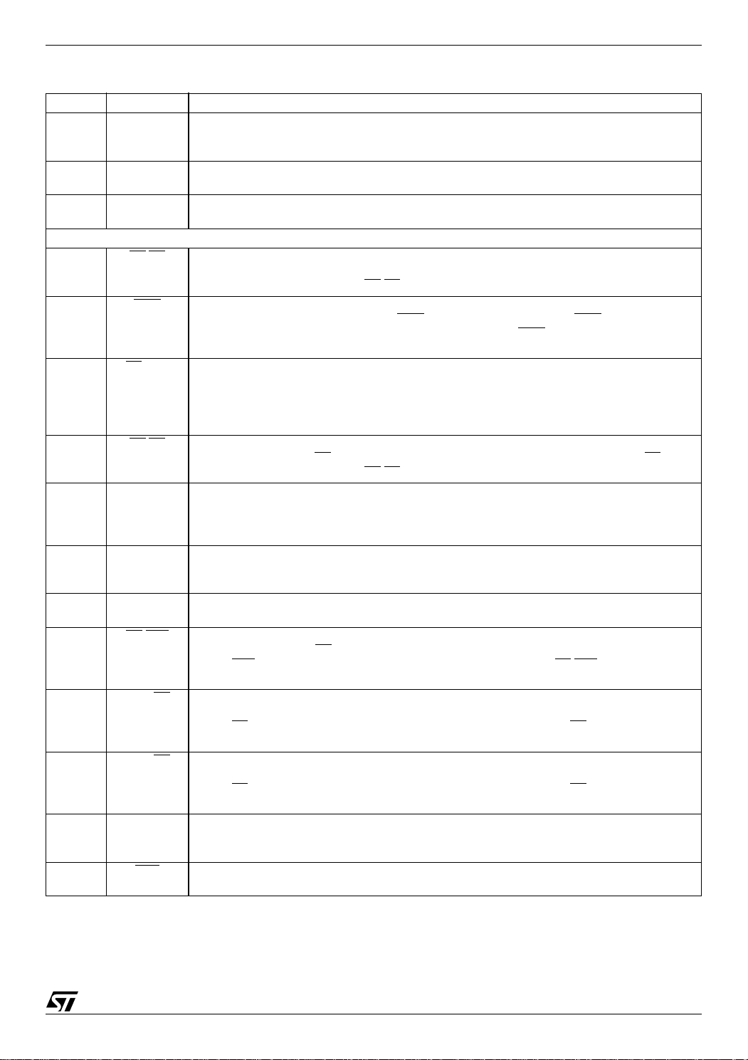
Figure 1. STA020D Professional & Consumer Modes Typical Connection Diagram.
EXTERNAL
CLOCK
MCK
FSYNC
AUDIO
DATA
PROCESSOR
µCONTROLLER
or
UNUSED
CHANNEL
STATUS BITS
CONTROL
SCK
SDATA
CBL
C
U
V
RST
5
7
6
8
15
10
11
9
16
8 DEDICATED C.S. BITS
STA020
+3.3V
19
VD+
18
24
23
22
21
20
17
GND
TRNPT
M0
M1
M2
TXP
TXN
0.1µF
SERIAL PORT
MODE SELECT
TRANSMITTER
CIRCUIT
D97AU600A
4/14

Obsolete Product(s) - Obsolete Product(s)
Figure 2. STA020D Typical Connection Diagram.
STA020
AUDIO
DATA
PROCESSOR
DECODER
SUBCODE
PORT
RESET
CONTROL
CHANNEL
STATUS BITS
CONTROL
FSYNC
SCK
SDATA
SBF
SBC
RST
EXTERNAL
CLOCK
MCK
7
6
8
V
9
10
U
11
15
16
8 DEDICATED C.S. BITS
5
STA020
+5V
19
VD+
18
23
22
21
20
17
GND
M0
M1
M2
TXP
TXN
0.1µF
SERIAL PORT
MODE SELECT
TRANSMITTER
CIRCUIT
D99AU989A
GENERAL DESCRIPTION
The STA020D is a monolithic CMOS circuit that encodes and transmits audio and digital data according
to the AES/EBU, IEC 958, S/PDIF, and EIAJ CP-340 interface standards. The chip accepts audio and control data separately; multiplex and biphase-mark encode the data internally and drive it, directly or through
a transformer, to a transmission line.
The STA020D has dedicated pins for the most important control bits and a serial input port for the C, U
and V bits.
Line Drivers
The differential line drivers for STA020D are low skew, low impedance, differential outputs capable of driving 110Ohm transmission lines. (RS422 line driver compatible).
They can also be disabled by resetting the device (RST = low).
STA020D DESCRIPTION
The STA020D accepts 16 to 24-bit audio samples through a serial port configured in one of seven formats;
provides several pins dedicated to particular channel status bits and allows all channel status, user and
validity bits to be serially input through port pins. This data is multiplexed, the parity bit is generated and
the bit stream is biphase-mark encoded and driven through an RS422 line driver.
The STA020D operates as a professional or consumer interface transmitter selectable by pin 2, PRO
. As
a professional interface device, the dedicated channel status input pins are defined according to the professional standard, and the CRC code (C.S. byte 23) can be internally generated.
As a consumer device, the dedicated channel status input pins are defined according to the consumer
standard. A submode provided under the consumer mode is compact disk, CD, mode. When transmitting
data from a compact disk, the CD subcode port can accept CD subcode data, extract channel status in-
5/14

Obsolete Product(s) - Obsolete Product(s)
STA020
formation from it, and transmit it as user data.
The master clock , MCK, controls timing for the entire chip and must be 128xFs. As an example, if stereo
data is input to the STA020D at 44.1kHz, MCK input must be 128 times that or 5.6448MHz.
Audio Serial Port
The audio serial port is used to enter audio data and consists of three pins: SCK, SDATA and FSYNC,
SCK clocks in SDATA, which is double buffered, while FSYNC delineates the audio samples and may indicate the particular channel, left or right. To support many different interfaces, M2, M1 and M0 select one
of seven different formats for the serial port. The coding is shown in Table 3 while the formats are shown
in Figure 3.
Format 0 and 1 are designed to interface with Crystal ADCs. Format 2 communicates with Motorola and
TI DSPs. Format 3 is reserved. Format 4 is compatible with the I2S standard. Formats 5 and 6 make the
STA020D look similar to existing 16- and 18-bit DACs and interpolation filters. Format 7 is an MSB-last
format and is conducive to serial arithmetic. SCK and FSYNC are outputs in Format 0 and inputs in all
other formats. In Format 2, the rising edge of FSYNC delineates samples and the falling edge must occur
a minimum of one bit period before or after the rising edge. In all formats except 2, FSYNC contains left/
right information requiring both edges of FSYNC to delineate samples. Formats 5 and 6 require a minimum
of 16- or 18-bit audio words respectively. In all formats other than 5 and 6, the STA020D can accept any
word length from 16 to 24 bits by adding leading zeros in format 7 and trailing zeros in the other formats,
or by restricting the number of SCK periods between active edges of FSYNC to the sample word length.
FSYNC must be derived from MCK, either through a DSP using the same clock or using counters. If
SFYNC moves (jitters) with respect to MCK by four MCK periods, the internal counters and CBL may be
reset.
Table 1. Audio Port Modes
M2 M1 M0 Format
0 0 0 0 - FSYNC & SCK Output
0 0 1 1 - Left/Right, 16-24 Bits
0 1 0 2 - Word Sync, 16-24 Bits
0113 - Reserved
100
1 0 1 5 - LSB Justified, 16 Bits
1 1 0 6 - LSB Justified, 18 Bits
1 1 1 7 - MSB Last, 16-24 Bits
4 - Left/Right, I
2
S Compatible
6/14

Obsolete Product(s) - Obsolete Product(s)
Figure 3. Audio Serial Port Formats.
FORMAT 0:
FSYNC(out)
SCK(out)
SDATA(in)
FORMAT 1:
FSYNC(in)
SCK(in)
SDATA(in)
FORMAT 2:
FSYNC(in)
SCK(in)
SDATA(in)
FORMAT 3:
(RESERVED)
FORMAT 4:
FSYNC(in)
SCK(in)
SDATA(in)
FORMAT 5:
FSYNC(in)
SCK(in)
SDATA(in)
FORMAT 6:
FSYNC(in)
SCK(in)
SDATA(in)
FORMAT 7:
FSYNC(in)
SCK(in)
SDATA(in)
LSB
LSB
MSB
LEFT RIGHT
MSB LSB MSB LSB MSB
LEFT RIGHT
MSB LSB MSB LSB MSB
LEFT RIGHT
MSB LSB MSB LSB MSB
LEFT RIGHT
MSB LSB MSB LSB MSB
LEFT RIGHT
MSB
LEFT RIGHT
MSB
LEFT RIGHT
LSB
LSB MSB LSB
16 Bits 16 Bits
LSB MSB LSB
18 Bits 18 Bits
MSB LSB MSB
D97AU604
STA020
C, U, V Serial Port
The serial input pins for channel status (C), user (U), and validity (V) are sampled during the first bit period
after the active edge of FSYNC for all formats except Format 4. Format 4 is sampled during the second
bit period (coincident with the MSB). In Figure 3, the arrows on SCK indicate when the C, U, and V bits
are sampled. The C, U, and V bits are transmitted with the audio sample entered before FSYNC edge that
sampled it. The V bit, as defined in the audio standards, is set to zero to indicate the audio data is suitable
for conversion to analog. Therefore, when the audio data is errored, or the data is not audio, the V bit
should be set high. The channel status serial input pin (C) is not available in consumer mode when the
CD subcode port is enabled (FC1 = FC0 = high). Any channel status data entered through the channel
status serial input (C) is logically OR’ed with the data entered through the dedicated pins or internally generated.
7/14

Obsolete Product(s) - Obsolete Product(s)
STA020
RST and CBL (TRNPT is low)
When RST
ST020 to the audio serial port, the transmit timing counters, which include CBL, are not enabled after RST
goes high until eight and one half SCK periods after reset is exited) of FSYNC. When FSYNC is configured
as a left/right signal (all defined formats except 2), the counters and CBL are not enabled until the right
sample is being transmitted). This guarantees that channel A is left and channel B is right as per the digital
audio interface specs.
As shown in Figure 4, channel block start output (CBL), can assist in serially inputting the C, U and V bits
as CBL goes high one bit period before the first bit of the preamble of the first sub-frame of the channel
status block is transmitted. This sub-frame contains channel status byte 0, bit 0. CBL returns low one bit
period before the start of the frame that contains bit 0 of channel status byte 16. CBL is not available when
the CD subcode port is enabled.
Figure 4 illustrates timing for stereo data input on the audio port. Notice how CBL rises while the right
channel data (Right 0) is input, but the previous left channel (Left 0) is being transmitted as the first subframe of the channel status block (starting with preamble Z). The C, U, and V input ports only need to be
valid for a short period after FSYNC changes. A sub-frame includes one audio sample while a frame includes a stereo pair. A channel status (C.S.) block contains 24 bytes of channel status and 384 audio samples (or 192 stereo pairs, or frames, of samples). Figure 4 shows the CUV ports as having left and right
bits (e.g. CUV0L, CUV0R). Since the C.S. block is defined as 192 bits, or one bit per frame, there are actually 2 C.S. blocks, one for channel A (left) and one for channel B (right). When inputting stereo audio
data, both blocks normally contain the same information, so C0L and C0R from the input port pin are both
channel status bit 0 of byte 0, which is defined as professional/consumer. These first two bits from the
port, C0L and C0R, are logically OR’ed with the inverse PRO
pin defined as C.S. bit 0.
Also, if in professional mode, C1
OR’ed with channel status input ports bits C1L and C1R. In similar fashion, C6
their respective input bits. Also, the C bits in CUV128L and CUV128R are both channel status block bit
128, which is bit 0 of channel status byte 16.
goes low, the differential line drivers are set to ground. In order to properly synchronize the
, since PRO is a dedicated channel status
, C6, C7 and C9 are dedicated C.S. pins. The inverse of C1 is logically
, C7 and C9 are OR’ed with
Figure 4. CBL and Transmitter Timing.
TRNPT high
CBL
TRNPT low
SDATA
FSYNC
TRNPT high
C,U,V
TRNPT low
TXP
TXN
LEFT 0 RIGHT 0 LEFT 1 LEFT 128 RIGHT 128 LEFT 0 RIGHT 0
C BITS FROM CPIN
CUV0L
CUV191R
C BITS OR'ed
w/PRO pin
RIGHT 191 LEFT 0 RIGHT 0
Preamble Y VUCP191R
CUV0R
CUV0L
Preamble Z
bit
Preamble Z Aux Data LSB Left 0 - Audio Data MSB
VUCP0L
CUV1L
CUV0R
C BITS OR'ed
w/C1 pin
Preamble Y
83740
CUV1R
CUV1L
VUCP0R
VUCP127R Preamble X
SUB-FRAME
CUV128R
CUV128L
BITS 0 of C.S.
BLOCK BYTE 16
LEFT
128
VUCP128L
RIGHT
128
Preamble Y
28 29 30 3127
V0 U0 C0 P0
CUV0L
CUV191R
CUV0R
CUV0L
D99AU990
8/14

Obsolete Product(s) - Obsolete Product(s)
STA020
Transparent Mode
In certain applications it is desirable to receive digital audio data with the STA120 and retransmit it with
the STA020D. In this case, channel status, user and validity information must pass through unaltered. For
studio environments, AES recommends that signal timing synchronization be maintained throughout the
studio. Frame synchronization of digital audio signals input to and output from a piece of equipment must
be within ±5%.
The transparent mode of the STA020D is selected by setting TRNPT, pin 24, high. In this mode, the CBL
pin becomes an input, allowing direct connection of the outputs of the STA120 to the inputs of the
STA020D as shown in Figure 18. The transmitter and receiver are synchronized by the FSYNC signal.
CBL specifies the start of a new channel status block boundry, allowing the transmit block structure to be
slaved to the block structure of the receiver.
In the transparent mode, C, U and V are now transmitted with the current audio sample as shown in Figure
5 (TRNPT high) and the dedicated channel status pins are ignored.
When FSYNC is a word clock (Format 2), CBL is sampled when left C, U, V are sampled. When FSYNC
is Left/Right, CBL is sampled when left C, U, V are sampled. The channel status block boundry is reset
when CBL transitions from low to high (based on two successive samples of CBL). MCK for the STA020D
is normally expected to be 128 times the sample frequency, in the trasparent mode MCK must be 256 Fs.
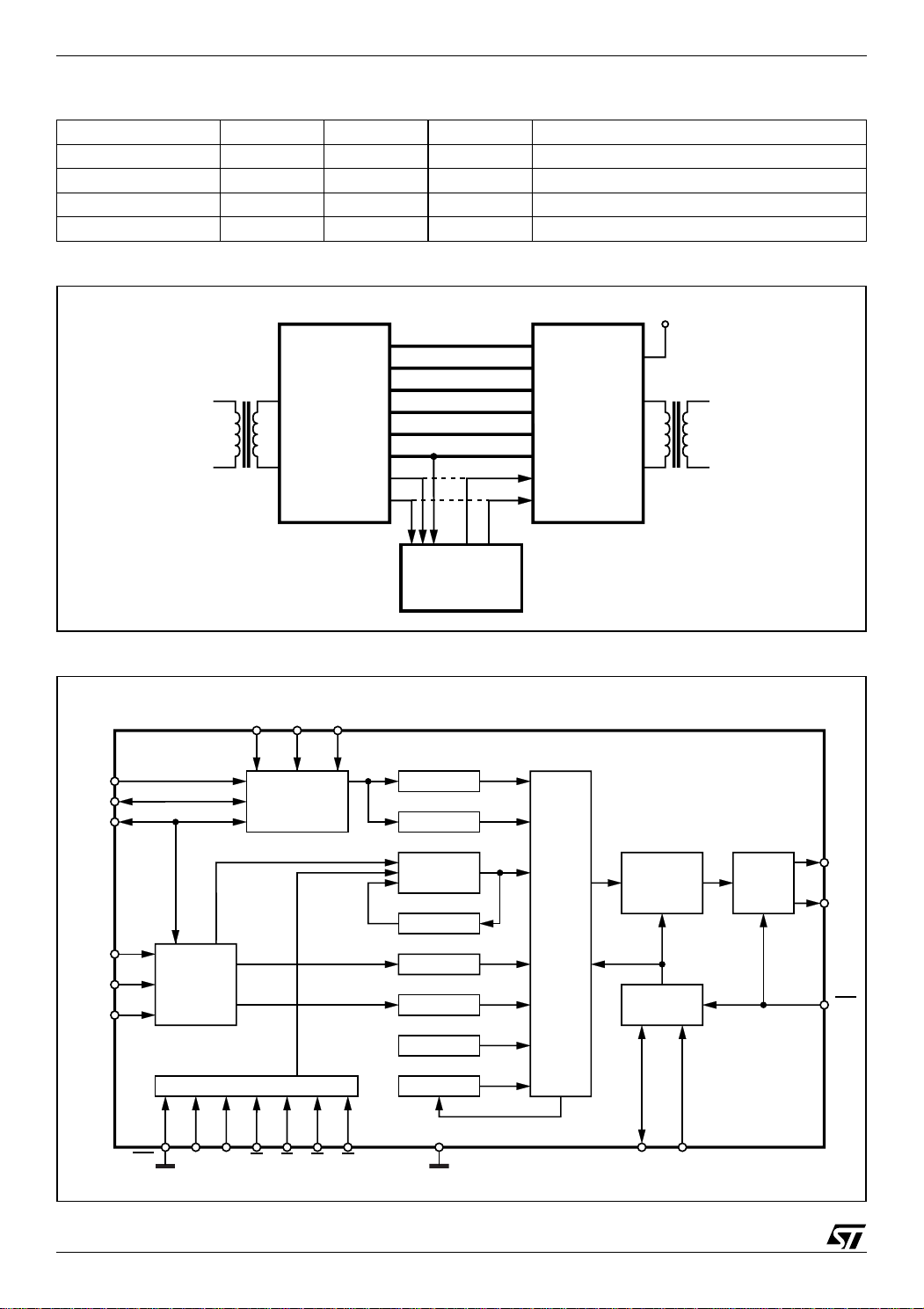
Professional Mode
Setting PRO
channel status bit 0 is transmitted as a one and bits 1, 2, 3, 4, 6, 7 and 9 can be controlled via dedicated
pins. The pins are actually the inverse of the identified bit.
For example, tying the C1
Overview of AES/EBU Digital Audio Interface Data Structures, C1
determine the sample frequency and C9 allows the encoded channel mode to be stereophonic. EM1 and
EM0 determine emphasis and encode C2
are read at the appropriate time and are logically OR’ed with data input on the channel status port, C. In
Transparent Mode, these dedicated channel status pins are ignored and channel status bits are input at
the C pin.
low places the STA020D in professional mode as shown in Figure 6. In professional mode,
pin low places a one in channel status bit 1. As shown in the application Note,
indicates audio/non-audio; C6 and C7
, C3, C4 as shown in Table 2. The dedicated channel status pins
Consumer Mode
Setting PRO
In consumer mode, channel status bit 0 is transmitted as a zero and channel status bits 2, 3, 8, 9, 15, 24
and 25 are controlled via dedicated pins.
The pins are actually the inverse of the bit so if pin C2
as a zero. Also, FC0 and FC1 are encoded versions of channel status bits 24 and 25, which define the
sample frequency.
When FC0 and FC1 are both high, the part is placed in a CD submode which activates the CD subcode
port. This submode is described in detail in the next section. Table 3 describes the encoding of C24 and
C25 through the FC1 and FC0 pins. According to AES/EBU standards, C2 is copy prohibit/permit. C3
specifies pre-emphasis, C8 and C9 define the category code and C15 identifies the generation status of
the transmitted material (i.e. first generation, second generation).
high places the STA020D in consumer mode which redefines the pins as shown in Figure 7.
is tied high, channel status bit 2 will be transmitted
Table 2. Emphasis Encoding
EM1 EM0 C2 C3 C4
00111
01110
10100
11000
9/14
Obsolete Product(s) - Obsolete Product(s)
STA020
Table 3. Sample Frequency Encoding
FC1 FC0 C24 C25 Comments
0 0 0 0 44.1kHz
0 1 0 1 48kHz
1 0 1 1 32kHz
1 1 0 0 44.1kHz, CD Mode
Figure 5. Transparent Mode Interface.
RXP
RXN
STA120
MCK
CBL
C
U
V
FSYNC
SCK
SDATA
V+
TRNPT
TXP
TXN
STA020
DATA
PROCESSING
D97AU605
Figure 6. Block Diagram - Professional Mode
PORT
LOGIC
M2
21
AUDIO
AUX
20
C Bits
CRC
U Bits
VALIDITY
MUX
BIPHASE
MARK
ENCODER
TIMING
LINE
DRIVER
TXP
TXN
17
16
RST
SDATA
SCK
FSYNC
M0 M1
23 22
8
6
7
10
C
11
U
V
REGISTERS
9
SERIAL
PREAMBLE
10/14
MUX
2141334112 15 5
PRO
EM0 EM1 C1 C6 C7 C9 CBL MCK
PARITY
24
TRNPT
D97AU607B

Obsolete Product(s) - Obsolete Product(s)
Figure 7. Block Diagram - Consumer Mode
STA020
SDATA
SCK
FSYNC
+3.3V
PORT
LOGIC
M2
21
AUDIO
AUX
C Bits
U Bits
VALIDITY
PREAMBLE
PARITY
MUX
BIPHASE
MARK
ENCODER
TIMING
DRIVER
LINE
D97AU606A
20
TXP
TXN
17
16
RST
M0 M1
23 22
8
6
7
10
C
11
U
V
REGISTERS
9
2
3 24 4 1 13 14 12 15 5
FC0 FC1 C2 C3 C8 C9 C15 CBL MCKPRO
SERIAL
MUX
11/14

Obsolete Product(s) - Obsolete Product(s)
STA020
DIM.
MIN. TYP. MAX. MIN. TYP. MAX.
A 2.35 2.65 0.093 0.104
A1 0.10 0.30 0.004 0.012
B 0.33 0.51 0.013 0.200
C 0.23 0.32 0.009 0.013
(1)
15.20 15.60 0.598 0.614
D
E 7.40 7.60 0.291 0.299
e 1.27 0.050
H 10.0 10.65 0.394 0.419
h 0.25 0.75 0.010 0.030
L 0.40 1.27 0.016 0.050
k 0˚ (min.), 8˚ (max.)
ddd 0.10 0.004
(1) “D” dimension does not include mold flash, protusions or gate
burrs. Mold flash, p rotusions or gate burrs shall no t exceed
0.15mm per side.
mm inch
OUTLINE AND
MECHANICAL DATA
Weight: 0.60gr
SO24
0070769 C
12/14

Obsolete Product(s) - Obsolete Product(s)
REVISION HISTORY
Date Revision Changes
14-Oct-2002 5 Technical Migration from ST-PRESS to EDOCS
26-Apr-2010 6 Major revision for revalidation process
STA020
13/14

Obsolete Product(s) - Obsolete Product(s)
STA020
Please Read Carefully:
Information in this document is provided solely in connection with ST products. STMicroelectronics NV and its subsidiaries (“ST”) reserve the
right to make changes, corrections, modifications or improvements, to this document, and the products and services described herein at any
time, without notice.
All ST products are sold pursuant to ST’s terms and conditions of sale.
Purchasers are solely responsible for the choice, selection and use of the ST products and services described herein, and ST assumes no
liability whatsoever relating to the choice, selection or use of the ST products and services described herein.
No license, express or implied, by estoppel or otherwise, to any intellectual property rights is granted under this document. If any part of this
document refers to any third party products or services it shall not be deemed a license grant by ST for the use of such third party products
or services, or any intellectual property contained therein or considered as a warranty covering the use in any manner whatsoever of such
third party products or services or any intellectual property contained therein.
UNLESS OTHERWISE SET FORTH IN ST’S TERMS AND CONDITIONS OF SALE ST DISCLAIMS ANY EXPRESS OR IMPLIED
WARRANTY WITH RESPECT TO THE USE AND/OR SALE OF ST PRODUCTS INCLUDING WITHOUT LIMITATION IMPLIED
WARRANTIES OF MERCHANTABILITY, FITNESS FOR A PARTICULAR PURPOSE (AND THEIR EQUIVALENTS UNDER THE LAWS
OF ANY JURISDICTION), OR INFRINGEMENT OF ANY PATENT, COPYRIGHT OR OTHER INTELLECTUAL PROPERTY RIGHT.
UNLESS EXPRESSLY APPROVED IN WRITING BY AN AUTHORIZED ST REPRESENTATIVE, ST PRODUCTS ARE NOT
RECOMMENDED, AUTHORIZED OR WARRANTED FOR USE IN MILITARY, AIR CRAFT, SPACE, LIFE SAVING, OR LIFE
SUSTAINING APPLICATIONS, NOR IN PRODUCTS OR SYSTEMS WHERE FAILURE OR MALFUNCTION MAY RESULT IN
PERSONAL INJURY, DEATH, OR SEVERE PROPERTY OR ENVIRONMENTAL DAMAGE. ST PRODUCTS WHICH ARE NOT
SPECIFIED AS "AUTOMOTIVE GRADE" MAY ONLY BE USED IN AUTOMOTIVE APPLICATIONS AT USER’S OWN RISK.
Resale of ST products with provisions different from the statements and/or technical features set forth in this document shall immediately void
any warranty granted by ST for the ST product or service described herein and shall not create or extend in any manner whatsoever, any
liability of ST.
ST and the ST logo are trademarks or registered trademarks of ST in various countries.
Information in this document supersedes and replaces all information previously supplied.
The ST logo is a registered trademark of STMicroelectronics. All other names are the property of their respective owners.
© 2010 STMicroelectronics - All rights reserved
STMicroelectronics group of companies
Australia - Belgium - Brazil - Canada - China - Czech Republic - Finland - France - Germany - Hong Kong - India - Israel - Italy - Japan -
Malaysia - Malta - Morocco - Philippines - Singapore - Spain - Sweden - Switzerland - United Kingdom - United States of America
www.st.com
14/14
 Loading...