

Page 1
STA013
MPEG 2.5 LAYER III AUDIODECODER
SINGLE CHIP MPEG2 LAYER 3 DECODER
SUPPORTING:
- All features specified for Layer III in ISO/IEC
11172-3(MPEG 1 Audio)
- All features specified for Layer III in ISO/IEC
13818-3.2(MPEG 2 Audio)
- Lowersamplingfrequenciessyntaxextension,
(notspecifiedby ISO) called MPEG2.5
DECODES LAYER III STEREO CHANNELS,
DUAL CHANNEL, SINGLE CHANNEL
(MONO)
SUPPORTING ALL THE MPEG 1 & 2 SAMPLING FREQUENCIES AND THE EXTENSION TO MPEG 2.5:
48, 44.1, 32, 24, 22.05, 16, 12, 11. 025, 8 KHz
ACCEPTS MPEG 2.5 LAYER III ELEMENTARY COMPRESSED BITSTREAM WITH
DATA RATE FROM 8 Kbit/s UP TO 320 Kbit/s
DIGITALVOLUMECONTROL
DIGITALBASS& TREBLECONTROL
SERIALBITSTREAMINPUTINTERFACE
ANCILLARY DATA EXTRACTIONVIA I2C IN-
TERFACE.
SERIAL PCM OUTPUT INTERFACE (I
AND OTHERFORMATS)
PLL FOR INTERNAL CLOCK AND FOR OUT-
PUT PCMCLOCK GENERATION
LOW POWERCONSUMPTION:
85mW AT 2.4V
CRC CHECK AND SYNCHRONISATION ER-
ROR DETECTION WITH SOFTWARE INDICATORS
2
C CONTROLBUS
I
LOW POWER3.3V CMOSTECHNOLOGY
10 MHz, 14.31818 MHz, OR 14.7456 MHz
EXTERNAL INPUT CLOCK OR BUILT-IN INDUSTRY STANDARD XTAL OSCILLATOR
DIFFERENT FREQUENCIES MAY BE SUPPORTED UPON REQUESTTOSTM
APPLICATIONS
PC SOUNDCARDS
MULTIMEDIA PLAYERS
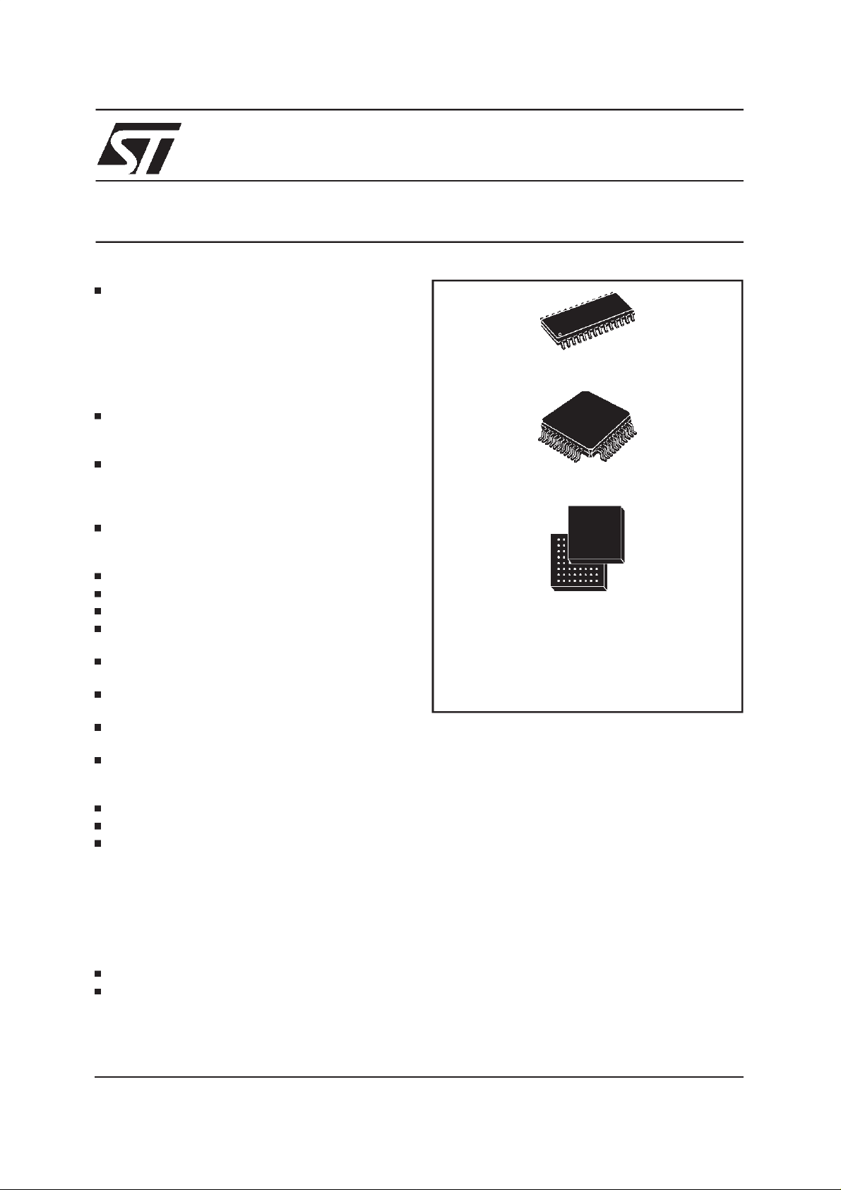
STA013B STA013T
SO28
TQFP44
LFBGA64
2
S
ORDERING NUMBERS: STA013$ (SO28)
STA013T$ (TQFP44)
STA013B$ (LFBGA 8x8)
DESCRIPTION
The STA013 is a fully integrated high flexibility
MPEG Layer III Audio Decoder, capable of decoding Layer III compressedelementary streams,
as specifiedin MPEG1 and MPEG 2 ISO standards. The devicedecodes alsoelementarystreams
compressedby using low samplingrates,as specifiedbyMPEG2.5.
STA013 receives the input data through a Serial
Input Interface. The decoded signal is a stereo,
mono, or dual channel digital output that can be
sent directly to a D/A converter, by the PCM Output Interface. This interface is software programmable to adapt the STA013 digital output to the
most common DACs architectures used on the
market.
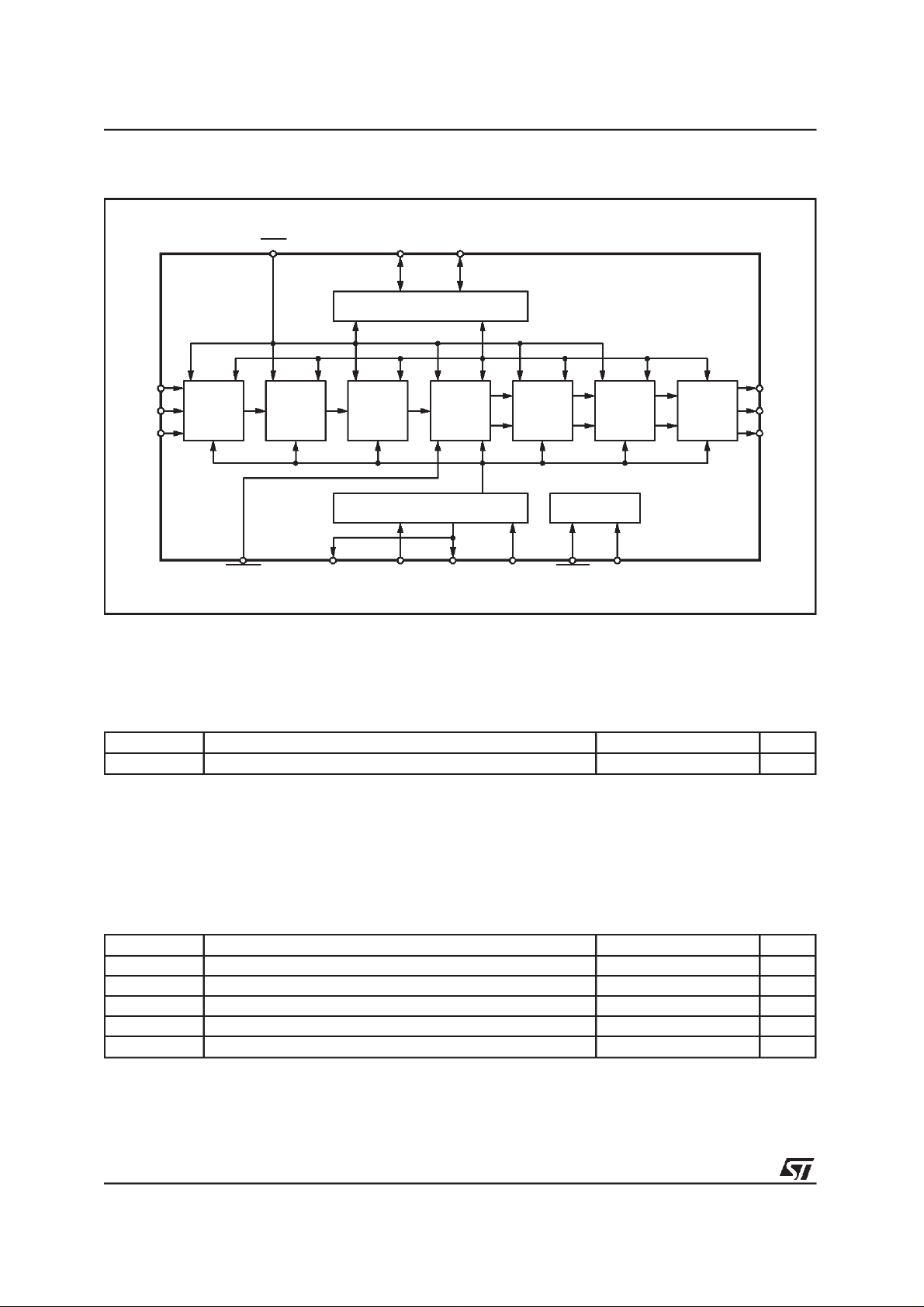
The functional STA013 chip partitioning is describedin Fig.1.
November 1999
1/38
Page 2
STA013 - STA013B - STA013T
Figure 1. Block Diagram:MPEG2.5 LayerIII Decoder HardwarePartitioning.
RESET SDA SCL
26 3 4
I2C CONTROL
5
SDI SDO
SCKR
BIT_EN
6
7
SERIAL
INPUT
INTERFACE
8282120122425
SRC_INT OUT_CLK/DATA_REQ XTI XTO OCLK TESTEN SCANEN
BUFFER
PARSER
SYSTEM &AUDIO CLOCKS TEST INTERFACE
2.5
MPEG
LAYER
DECODER
CORE
III
CHANNEL
CONFIG.
&
VOLUME
CONTROL
OUTPUT
BUFFER
PCM
OUTPUT
INTERFACE
D98AU965
THERMAL DATA
Symbol Parameter Value Unit
R
th j-amb
Thermal resistance Junction to Ambient 85 °C/W
9
10
SCKT
11
LRCKT
ABSOLUTE MAXIMUM RATINGS
Symbol Parameter Value Unit
Power Supply -0.3 to 4 V
Voltage on Input pins -0.3 to VDD+0.3 V
Voltage on output pins -0.3 to VDD+0.3 V
Storage Temperature -40 to +150 °C
Operative ambient temp -20 to +85 °C
2/38
V
DD
V
i
V
O
T
stg
T
oper
Page 3
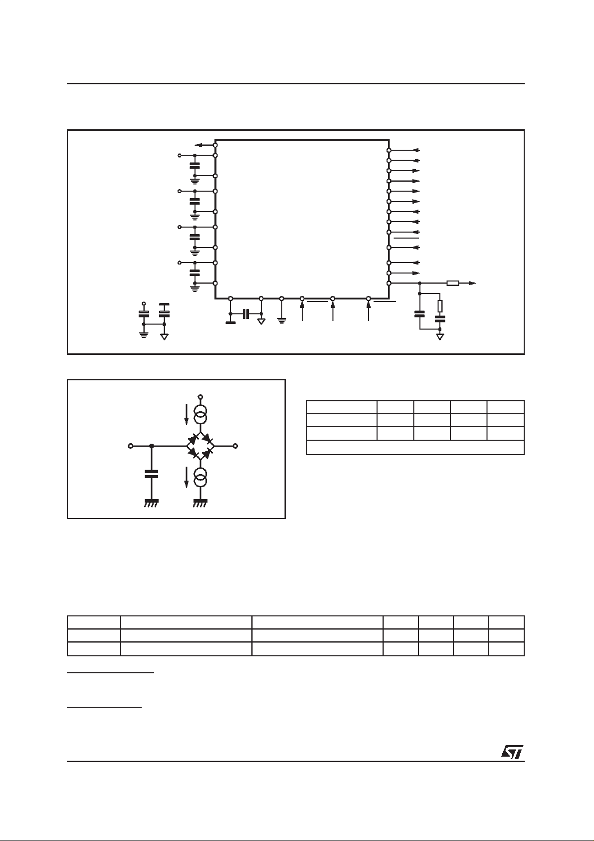
Figure 2. Pin Connection
STA013 - STA013B - STA013T
N.C.
LRCKT
OCLK
N.C.
VSS_2
VDD_2
VSS_3
VDD_3
N.C.
PVDD
PVSS
VDD_1
VSS_1
SCL
SDI
SCKR
BIT_EN
SRC_INT
SDO
SCKT
LRCKT
OCLK
VSS_2
VDD_2
1
2
3
4
5
6
7
8
9
10
1
2
3
4
5
6
SO28
7
8
9
10
11
12
13
D98AU911A
SRC_INT
N.C.
SDO
N.C.
SCKT
44 43 42 41 3940 38 37 36 35 34
TQFP44
12 13 14 15 16
XTI
N.C.
FILT
XTO
N.C.
28
27
26
25
24
23
22
21
20
19
18
17
16
1514
N.C.
SCKR
N.C.
BIT_EN
N.C.
171118 19 20 21 22
N.C.
N.C.
N.C.
VSS_4
VDD_4
OUT_CLK/DATA_REQ
VSS_5
RESETSDA
SCANEN
TESTEN
VDD_4
VSS_4
XTI
XTO
FILT
PVSS
PVDD
VDD_3
VSS_3
SDI
33
N.C.
32
SCL
31
SDA
30
VSS_1
29
VDD_1
28
N.C.
27
OUT_CLK/DATA_REC
26
VSS_5
25
RESET
24
SCANEN
23
N.C.
D99AU1019
TESTEN
12345678
A1 = SDI
A
B
C
D
E
F
G
H
B2 = SCKR
D4 = BIT_EN
D1 = SRC_INT
E2 = SDO
F2 = SCKT
H1 = LRCKT
H3 = OCLK
F3 = VSS_2
VDD_2
E4 =
G4 = VSS_3
VDD_3
G5 =
F5 = PVDD
G6 = PVSS
D99AU1085
G7 = FILT
G8 = XTO
F7 = XTI
E7 = VSS4
VDD4
C8 =
D7 = TESTEN
A7 =
SCANEN
B6 = RESET
A5 = VSS5
C5 = OUT_CLK/DATA_REQ
VDD1
B5 =
B4 = VSS1
A4 = SDA
B3 = SCL
LFBGA64
3/38
Page 4
STA013 - STA013B - STA013T
PIN DESCRIPTION
SO28 TQFP44 LFBGA64 Pin Name Type Function PAD Description
1 29 B5 VDD_1 Supply Voltage
2 30 B4 VSS_1 Ground
3 31 A4 SDA I/O i
4 32 B3 SCL I I
5 34 A1 SDI I Receiver Serial Data CMOS Input Pad Buffer
6 36 B2 SCKR I Receiver Serial Clock CMOS Input Pad Buffer
7 38 D4 BIT_EN I Bit Enable CMOSInputPad Buffer
8 40 D1 SRC_INT I Interrupt Line For S.R. Control CMOS Input Pad Buffer
9 42 E2 SDO O Transmitter SerialData (PCM
10 44 F2 SCKT O Transmitter Serial Clock CMOS 4mA Output Drive
11 2 H1 LRCKT O Transmitter Left/Right Clock CMOS 4mA Output Drive
12 3 H3 OCLK I/O Oversampling Clock for DAC CMOS Input Pad Buffer
13 5 F3 VSS_2 Ground
14 6 E4 VDD_2 Supply Voltage
15 7 G4 VSS_3 Ground
16 8 G5 VDD_3 Supply Voltage
17 10 F5 PVDD PLL Power
18 11 G6 PVSS PLL Ground
19 12 G7 FILT O PLL Filter Ext. Capacitor Conn.
20 13 G8 XTO O Crystal Output CMOS 4mA Output Drive
21 15 F7 XTI I Crystal Input (Clock Input) Specific Level Input Pad
22 19 E7 VSS_4 Ground
23 21 C8 VDD_4 Supply Voltage
24 22 D7 TESTEN I Test Enable CMOSInputPad Buffer
25 24 A7 SCANEN I Scan Enable CMOS Input Pad Buffer
26 25 B6 RESET I System Reset CMOSInputPad Buffer
27 26 A5 VSS_5 Ground
28 27 C5 OUT_CLK/
DATA_REQ
Note: SRC_INT signal is used by STA013 internalsoftware inBroadcast Modeonly;in Multimedia mode SRC_INT must be connected to
In functionalmodeTESTEN must be connected to VDD,SCANEN to ground.
V
DD
2
C Serial Data + Acknowledge CMOS Input Pad Buffer
CMOS 4mA Output Drive
2
C Serial Clock CMOS Input Pad Buffer
withpull up
CMOS 4mA Output Drive
Data)
CMOS 4mA Output Drive
(see paragraph 2.1)
withpull up
withpull up
O Buffered Output Clock/
CMOS 4mA Output Drive
Data Request Signal
4/38
Page 5

STA013 - STA013B - STA013T
1. ELECTRICALCHARACTERISTICS:VDD=2.4V±0.3V;T
amb
= 0 to 70°C;Rg = 50Ωunlessotherwise
specified
DC OPERATINGCONDITIONS
Symbol Parameter Value
V
T
Power Supply Voltage 2.7 to 3.6V
DD
Operating Junction Temperature -20 to 125°C
j
GENERAL INTERFACE ELECTRICALCHARACTERISTICS
Symbol Parameter Test Condition Min. Typ. Max. Unit Note
I
IL
Low Level Input Current
Vi= 0V -10 10 µA1
Without pull-up device
I
IH
High Level Input Current
Vi=VDD= 3.6V -10 10
A1
µ
Without pull-up device
V
esd
Note 1: The leakage currents are generally very small, < 1nA. The value given here is a maximum thatcan occur after an electrostatic stress
on the pin.
Note 2: Human Body Model.
Electrostatic Protection Leakage < 1µA 2000 V 2
DC ELECTRICAL CHARACTERISTICS
Symbol Parameter Test Condition Min. Typ. Max. Unit Note
V
IL
V
IH
V
ol
V
oh
Low Level Input Voltage 0.2*V
High Level Input Voltage 0.8*VDD V
Low Level Output Voltage Iol= Xma 0.4V V 1, 2
High Level Output Voltage 0.85*V
DD
V
DD
V1,2
Note 1: Takes intoaccount 200mV voltage drop in both supply lines.
Note 2: X is the source/sink current under worst case conditions and is reflected in the name of the I/O cell according to the drive capability.
Symbol Parameter Test Condition Min. Typ. Max. Unit Note
I
pu
R
pu
Pull-up current Vi= 0V; pin numbers 7, 24
Equivalent Pull-up
and 26; V
DD
=3V
-25 -66 -125 µA1
50 kΩ
Resistance
Note 1: Min. condition: VDD= 2.4V, 125°C Min process
Max. condition: V
DD = 3.6V, -20°C Max.
POWERDISSIPATION
Symbol Parameter Test Condition Min. Typ. Max. Unit Note
PD Power Dissipation
@V
=3V
DD
Sampling_freq ≤24 kHz 76 mW
Sampling_freq≤32 kHz 79 mW
Sampling_freq≤48 kHz 85 mW
5/38
Page 6
STA013 - STA013B - STA013T
Figure 3. Test Circuit
OUT_CLK/DATA_REQ
4.7µF 4.7µF
V
DD
100nF
V
V
DD
100nF
V
V
DD
100nF
V
V
DD
100nF
V
V
PV
DD
DD
PV
V
SS
SS
Figure 4. Test Load Circuit
I
OL
OUTPUT
SDA
3
24
4
9
10
11
12
5
6
7
8
21
20
19
TESTEN
SCL
SDO
SCKT
LRCKT
OCLK
SDI
SCKR
BIT_EN
SCR_INT
XTI
XTO
470pF
OL
10K
1K
4.7nF
PV
SS
I
OH
C
V
L
REF
1
SS
SS
SS
SS
2
14
13
16
15
23
22
17 18 272826
100nF
PV
V
DD
PV
DD
25
RESET
SS
SCANEN
D98AU966
Test Load
Output I
SDA 1mA 100pF 3.6V
Other Outputs 100µA 100µA 100pF 1.5V
V
REF
C
I
L
OH
D98AU967
2. FUNCTIONALDESCRIPTION
2.1 - Clock Signal
The STA013 input clock is derivated from an external source or from a industry standard crystal
oscillator, generating input frequencies of 10,
14.31818 or 14.7456 MHz.
Other frequencies may be supported upon request to STMicroelectronics. Each frequency is
supported by downloading a specific configuration file, providedby STM
XTI is an input Pad with specific levels.
Symbol Parameter Test Condition Min. Typ. Max. Unit
V
IL
V
IH
Low Level Input Voltage VDD-1.8 V
High Level Input Voltage VDD-0.8 V
CMOS compatibility
The XTI pad low and high levels are CMOS compatible; XTI pad noise margin is better than typical
CMOS pads.
TTL compatibility
The XTI padlow levelis compatiblewith TTL while the high level is not compatible(for example if V
DD =
3V TTL min high level = 2.0V whileXTI min high level = 2.2V)
6/38
Page 7
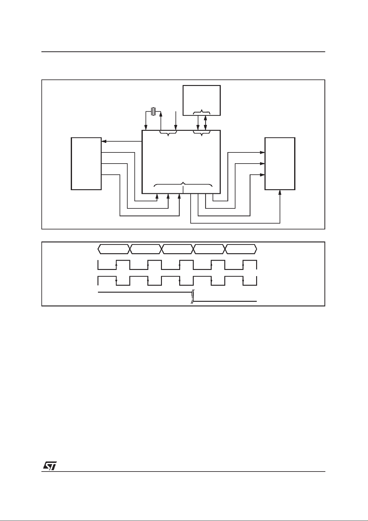
Figure 5. MPEG DecoderInterfaces.
STA013 - STA013B - STA013T
µP
DATA_REQ
SDI
DATA
SOURCE
D98AU912
SCKR
BIT_EN
Figure 6. SerialInput Interface Clocks
SDI
SCKR
SCKR
XTO
XTI FILT
PLL
MPEG
DECODER
SERIAL AUDIO INTERFACE
RX TX
IIC
SCL SDA
IIC
DATA IGNORED
SDO
SCKT
LRCKT
DAC
OCLK
SCLK_POL=0
SCLK_POL=4
BIT_EN
D98AU968A
2.2 - SerialInput Interface
STA013 receives the input data (MSB first)
thought the Serial Input Interface (Fig.5). It is a
serial communication interface connected to the
SDI (Serial Data Input) and SCKR (Receiver Serial Clock).
The interface can be configured to receive data
sampled on both rising and falling edge of the
SCKR clock.
The BIT_EN pin, when set to low, forces the bitstream input interface to ignore the incoming
N
data. For proper operation Bit-E
line shold be
toggled only when SCR is stable low (for both
SCLK_POL configuration) The possible configurations are described in Fig. 6.
DATA IGNOREDDATA VALID
2.3 - PLL& ClockGeneratorSystem
When STA013 receives the input clock, as described in Section 2.1, and a valid layer III input
bit stream, the internal PLL locks, providing to the
DSP Core the master clock (DCLK), and to the
Audio Output Interface the nominal frequenciesof
the incoming compressedbit stream.The STA013
PLLblockdiagramisdescribedinFigure7.
The audio sample rates are obtained dividing the
oversampling clock (OCLK) by software programmable factors. The operation is done by STA013
embedded software and it is transparent to the
user.
The STA013 PLL can drive directly most of the
commercial DACs families, providing an over
sampling clock, OCLK, obtained dividingthe VCO
frequencywith a softwareprogrammabledividers.
7/38
Page 8
STA013 - STA013B - STA013T
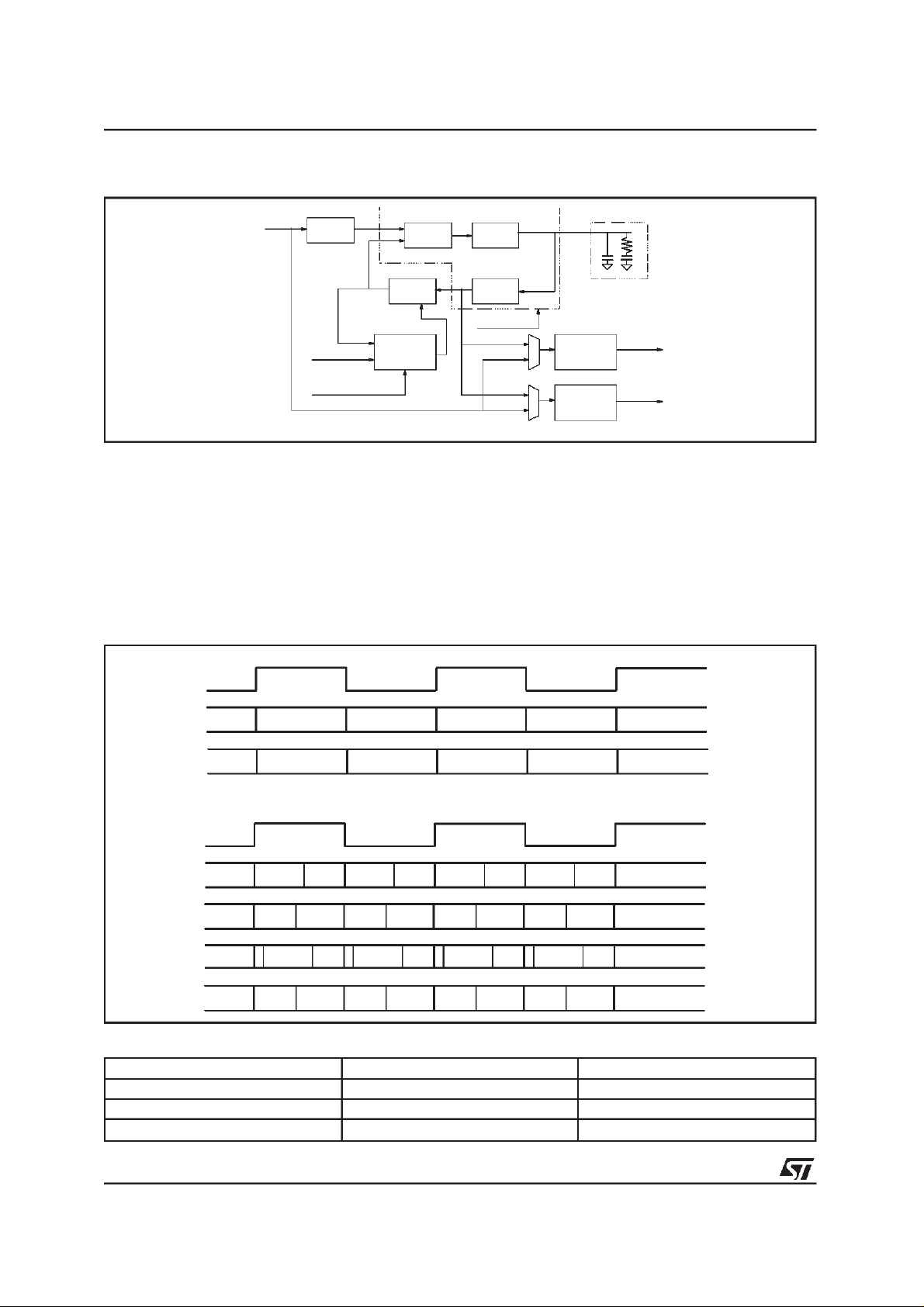
Figure 7. PLL and Clocks GenerationSystem
XTI
N
PFD CP
M
FRAC
Update FR AC
Switching
Circuit
2.4 - PCM Output Interface
The decoded audio data are output in serial PCM
format. The interface consists of the followingsignals:
SDO PCM SerialData Output
SCKT PCMSerial Clock Output
LRCLK Left/RightChannel SelectionClock
The output samples precision is selectable from
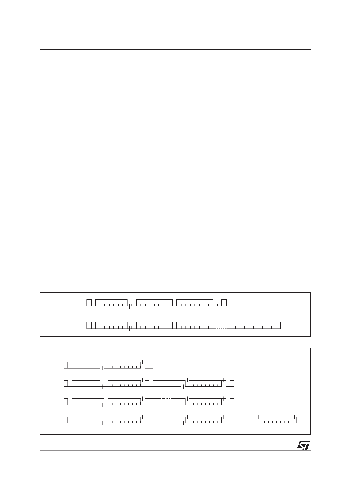
Figure 8. PCM Output Formats
16 SCLK Cycles
LRCKT
16 SCLK Cycles
R
CC
VCO
Disable PLL
OCLK
X
XTI2OCLK
DCLK
S
XTI2DSPCLK
16 to 24 bits/word, by settingthe output precision
with PCMCONF (16, 18, 20 and 24 bits mode)
register. Data can be output either with the most
significant bit first (MS) or least significant bit first
(LS), selected by writing into a flag of the
PCMCONFregister.
Figure 8 gives a description of the several
STA013PCM Output Formats.
The sample rates set decoded by STA013 is describedin Table1.
16 SCLK Cycles
16 SCLK Cycles
16 SCLK Cycles
SDO
SDO
M
S
L
S
M
L
S
S
L
M
S
S
32 SCLK Cycles
LRCKT
SDO
SDO
SDO
SDO
M
L
S
S
M
0
S
L
M
0
S
S
M
S
32 SCLK Cycles
M
S
L
S
M
0
00
S
L
MSBMSB MSB MSB
S
Table 1: MPEG SamplingRates (KHz)
MPEG 1 MPEG 2 MPEG 2.5
48 24 12
44.1 22.05 11.025
32 16 8
L
M
S
S
L
M
S
S
32 SCLK Cycles
M
L
S
S
M
L
S
S
PCM_ORD = 0
L
S
PCM_PRECis 16 bit mode
PCM_ORD = 1
M
S
PCM_PRECis 16 bit mode
32 SCLK Cycles
32 SCLK Cycles
L
00
S
L
M
S
S
L
S
L
M
S
S
L
M
S
S
M
00
S
M
0
S
MSL
M
0
L
S
L
00
S
S
L
S
S
M
0
S
L
M
0
S
S
M
S
PCM_FORMAT = 1
0
PCM_DIFF = 1
PCM_FORMAT = 0
L
S
PCM_DIFF = 0
PCM_FORMAT = 0
PCM_DIFF = 1
PCM_FORMAT = 1
L
S
PCM_DIFF = 1
8/38
Page 9
STA013 - STA013B - STA013T
2.5 - STA013Operation Mode
The STA013 can work in two different modes,
called Multimedia Mode and BroadcastMode.
In Multimedia Mode, STA013 decodes the in-
coming bitstream, acting as a master of the data
communicationfrom the source to itself.
This control is done by a specific buffer management, controlled by STA013embeddedsoftware.
The data source, by monitoring the DATA_REQ
line, send to STA013 the input data, when the
signal ishigh (default configuration).
The communication is stopped when the
DATA_REQline is low.
In this mode the fractional part of the PLL is disabled and the audio clocks are generated at
nominal rates. Fig. 9 describes the default
DATA_REQsignalbehaviour.
Programming STA013 it is possible to invert the
polarity of the DATA_REQ line (register
REQ_POL).
Figure 9.
SOURCE STOPS TRANSMITTING DATA SOURCE STOPS TRANSMITTING DATA
DATA_REQ
SOURCE SEND DATA TO STA013
D98AU913
the configuration register of the device. The DAC
connected to STA013 can be initialised during
this mode (set MUTE to 1).
PLAY MUTE Clock State PCM Output
X 0 Not Running 0
X 1 Running 0
Init Mode
”PLAY” and ”MUTE” changes are ignored in this
mode. The internal state of the decoder will be
updated only when the decoder changes from the
state ”init” to the state ”decode”. The ”init” phase
ends when the first decoded samples are at the
output stage of the device.
Decode Mode
This mode is completely described by the following table:
PLAY MUTE Clock State
0 0 Not Running 0 No
0 1 Running 0 No
1 0 Running Decoded
1 1 Running 0 Yes
PCM
Output
Samples
Decoding
Yes
In Broadcast Mode, STA013 works receiving a
bitstream with the input speed regulated by the
source. In this configuration the source has to
guarantee that the bitrate is equivalent to the
nominal bitrate of the decoded stream.
To compensate the differencebetween the nominal and the real sampling rates, the STA013 embedded software controls the fractional PLL operation. Portable or Mobile applications need
normally to operate in Broadcast Mode. In both
modes the MPEG Synchronisation is automatic
and transparent to the user. To operate in Multimedia mode, the STA013, pin nr. 8, SCR-INT
must be connected to VDD on the application
board.
2.6 - STA013Decoding States
There are three different decoder states: Idle,
Init, and Decode. Commands to change the de-
coding states are described in the STA013 I
2
C
registers description.
Idle Mode
In this mode the decoder is waiting for the RUN
command. This mode should be used to initialise
3-I2C BUS SPECIFICATION
The STA013 supports the I
2
C protocol. This protocol defines any device that sends data on to the
bus as a transmitter and any device that reads
the data as a receiver. The device that controls
the data transfer is known as the master and the
others as the slave. The master always starts the
transfer and provides the serialclock forsynchronisation. The STA013 is always a slave device in
all its communications.
3. 1 - COMMUNICATIONPROTOCOL
3.1.0 - Data transition or change
Data changes on the SDA line must only occur
when the SCL clock is low. SDA transition while
the clock is high are used to identify START or
STOP condition.
3.1.1 - Start condition
START is identified by a high to low transition of
the data bus SDA signal while the clock signal
SCL is stable in the high state.
A START condition must precede any command
fordatatransfer.
9/38
Page 10
STA013 - STA013B - STA013T
3.1.2 - Stop condition
STOP is identified by low to high transition of the
data bus SDA signal while the clock signal SCL is
stable in the high state. A STOP condition terminates communications between STA013 and the
bus master.
3.1.3 - Acknowledge bit
An acknowledgebit is used toindicate a successful data transfer. The bus transmitter, either master or slave, releases the SDA bus after sending
8 bit of data.
During the 9th clock pulse the receiver pulls the
SDA bus low to acknowledgethe receipt of 8 bits
of data.
3.1.4 - Data input
During the data input the STA013 samples the
SDA signal on the rising edge of the clock SCL.
For correct device operation the SDA signal has
to be stable during the rising edge of the clock
and the data can change only when the SCL line
is low.
3.2 - DEVICEADDRESSING
To start communication between the master and
the STA013, the master must initiate with a start
condition. Following this, the master sends onto
the SDA line 8 bits (MSB first) corresponding to
the device select address and read or write
mode.
Figure 10. Write Mode Sequence
The 7 most significant bits are the device address
identifier, corresponding to the I
2
C bus definition.
For the STA013these are fixed as 1000011.
The 8th bit (LSB) is the read or write operation
RW, this bit is set to 1 in read mode and 0 for
write mode. After a STARTcondition the STA013
identifies on the bus the device address and, if a
match is found, it acknowledgesthe identification
on SDA bus during the 9th bittime. The following
byte after the device identification byte is the internal space address.
3.3 - WRITEOPERATION(see fig. 10)
Following a START condition the master sends a
deviceselectcode with the RW bit set to 0.
The STA013 acknowledges this and waits for the
byte ofinternal address.
After receiving the internal bytes address the
STA013again responds with an acknowledge.
3.3.1 - Byte write
In the bytewrite mode the mastersends one data
byte, this is acknowledged by STA013. The master then terminates the transfer by generating a
STOP condition.
3.3.2 - Multibytewrite
The multibyte write mode can start from any internal address. The transfer is terminated by the
master generatinga STOPcondition.
BYTE
WRITE
MULTIBYTE
WRITE
START
START RW
DEV-ADDR
DEV-ADDR
Figure 11. Read Mode Sequence
ACK
CURRENT
ADDRESS
RANDOM
ADDRESS
SEQUENTIAL
CURRENT
SEQUENTIAL
RANDOM
10/38
READ
READ
READ
READ
DEV-ADDR
START
DEV-ADDR
START RW
START
START RW
DEV-ADDR
DEV-ADDR
RW=
HIGH
DATA
RW
ACK
SUB-ADDR
ACK
DATA
ACK
SUB-ADDR
ACK
RW
ACK
NO ACK
ACK
START RW
ACK
ACK
START RW
SUB-ADDR
SUB-ADDR
STOP
DATA
DEV-ADDR
DEV-ADDR
ACK
ACK
ACK
ACK
ACK
DATA IN
DATA IN
DATA
DATA
DATA
ACK
ACK
STOP
NO ACK
NO ACK
ACK
D98AU825B
STOP
STOP
DATA
DATA IN
ACK
ACK NO ACK
D98AU826A
STOP
DATA
STOP
Page 11
STA013 - STA013B - STA013T
3.4 - READOPERATION(see Fig. 11)
3.4.1 - Currentbyte addressread
The STA013 has an internal byte address
counter. Each time a byte is written or read, this
counter is incremented.
For the current byte address read mode, following a START condition the master sends the device addresswith the RW bit setto 1.
The STA013 acknowledges this and outputs the
byte addressed by the internal byte address
counter. The master does not acknowledge the
received byte, but terminates the transfer with a
STOP condition.
3.4.2 - Sequentialaddress read
This mode can be initiated with either a current
address read or a random address read. However in this case the master does acknowledge
the data byte output and the STA013 continues to
output the next byte in sequence.
To terminate the streams of bytes the master
does not acknowledgethe last received byte, but
terminatesthe transfer with a STOP condition.
The output data stream is from consecutive byte
addresses, with the internal byte address counter
automaticallyincrementedafter one byte output.
2
4-I
C REGISTERS
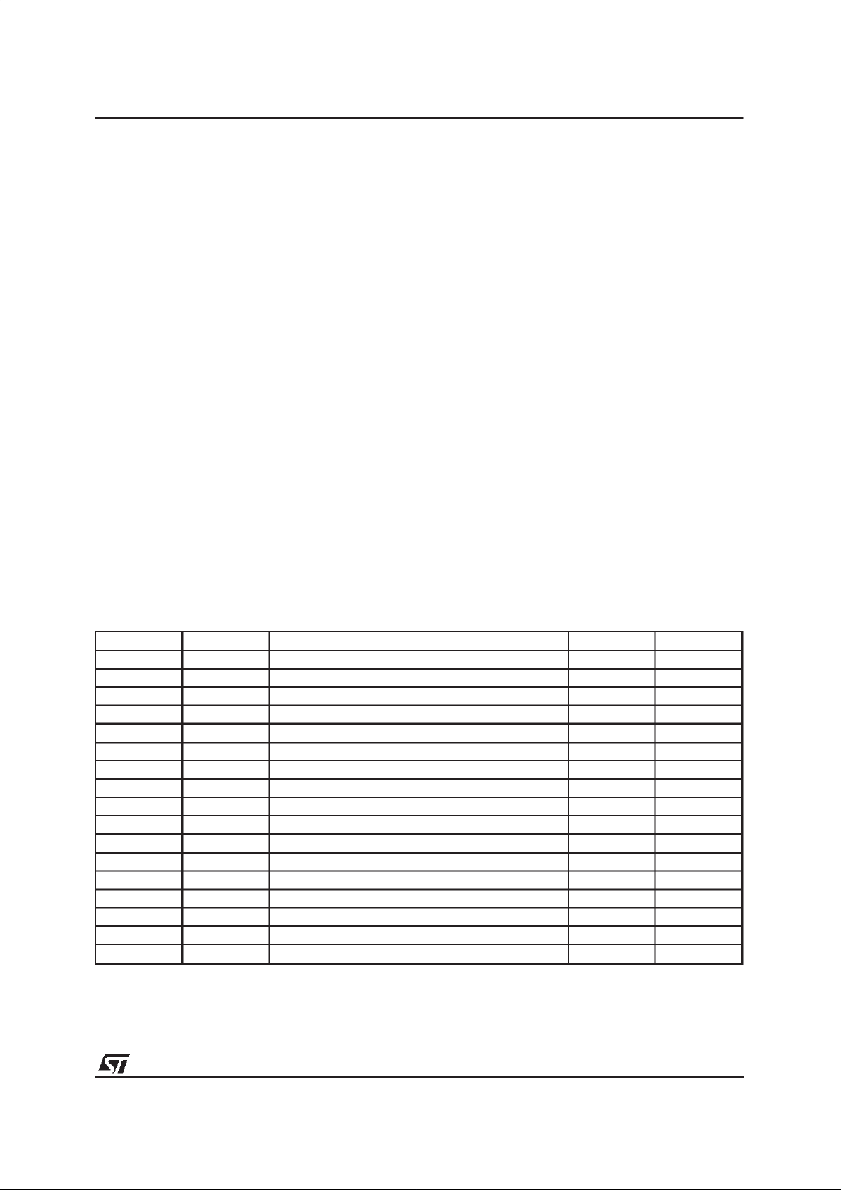
The following table gives a description of the
MPEGSource Decoder (STA013)register list.
The first column (HEX_COD) is the hexadecimal
code for the sub-address.
The second column (DEC_COD) is the decimal
code.
The third column (DESCRIPTION) is the description of the informationcontained in the register.
The fourth column (RESET) inidicate the reset
value if any. When no reset value is specifyed,
the default is ”undefined”.
The fifth column (R/W) is the flag to distinguish
register ”read only” and ”read and write”, and the
useful size of the register itself.
Each register is 8 bitwide. The master shall operate readingor writing on 8 bits only.
2
I
C REGISTERS
HEX_COD DEC_COD DESCRIPTION RESET R/W
$00 0 VERSION R (8)
$01 1 IDENT 0xAC R (8)
$05 5 PLLCTL [7:0] 0xA1 R/W (8)
$06 6 PLLCTL [20:16] (MF[4:0]=M) 0x0C R/W (8)
$07 7 PLLCTL [15:12] (IDF[3:0]=N) 0x00 R/W (8)
$0B 11 reserved
$0C 12 REQ_POL 0x01 R/W (8)
$0D 13 SCLK_POL 0x04 R/W (8)
$0F 15 ERROR_CODE 0x00 R (8)
$10 16 SOFT_RESET 0x00 W (8)
$13 19 PLAY 0x01 R/W(8)
$14 20 MUTE 0x00 R/W(8)
$16 22 CMD_INTERRUPT 0x00 R/W(8)
$18 24 DATA_REQ_ENABLE 0x00 R/W(8)
$40 64 SYNCSTATUS 0x00 R (8)
$41 65 ANCCOUNT_L 0x00 R (8)
$42 66 ANCCOUNT_H 0x00 R (8)
11/38
Page 12

STA013 - STA013B - STA013T
I2C REGISTERS (continued)
HEX_COD DEC_COD DESCRIPTION RESET R/W
$43 67 HEAD_H[23:16] 0x00 R(8)
$44 68 HEAD_M[15:8] 0x00 R(8)
$45 69 HEAD_L[7:0] 0x00 R(8)
$46 70 DLA 0x00 R/W (8)
$47 71 DLB 0xFF R/W (8)
$48 72 DRA 0x00 R/W (8)
$49 73 DRB 0xFF R/W (8)
$50 80 MFSDF_441 0x00 R/W (8)
$51 81 PLLFRAC_441_L 0x00 R/W (8)
$52 82 PLLFRAC_441_H 0x00 R/W (8)
$54 84 PCM DIVIDER 0x03 R/W (8)
$55 85 PCMCONF 0x21 R/W (8)
$56 86 PCMCROSS 0x00 R/W (8)
$59 89 ANC_DATA_1 [7:0] 0x00 R (8)
$5A 90 ANC_DATA_2 [15:8] 0x00 R (8)
$5B 91 ANC_DATA_3 [23:16] 0x00 R (8)
$5C 92 ANC_DATA_4 [31:24] 0x00 R (8)
$5D 93 ANC_DATA_5 [39:32] 0x00 R (8)
$61 97 MFSDF (X) 0x07 R/W (8)
$63 99 DAC_CLK_MODE 0x00 R/W (8)
$64 100 PLLFRAC_L 0x46 R/W (8)
$65 101 PLLFRAC_H 0x5B R/W (8)
$67 103 FRAME_CNT_L 0x00 R (8)
$68 104 FRAME_CNT_M 0x00 R (8)
$69 105 FRAME_CNT_H 0x00 R (8)
$6A 106 AVERAGE_BITRATE 0x00 R (8)
$71 113 SOFTVERSION R (8)
$72 114 RUN 0x00 R/W (8)
$77 119 TREBLE_FREQUENCY_LOW 0x00 R/W (8)
$78 120 TREBLE_FREQUENCY_HIGH 0x00 R/W (8)
$79 121 BASS_FREQUENCY_LOW 0x00 R/W (8)
$7A 122 BASS_FREQUENCY_HIGH 0x00 R/W (8)
$7B 123 TREBLE_ENHANCE 0x00 R/W (8)
$7C 124 BASS_ENHANCE 0x00 R/W (8)
$7D 125 TONE_ATTEN 0x00 R/W (8)
Note:
1) The HEX_COD is the hexadecimal adress that the microcontroller has togenerate to access the information.
2) RESERVED: register used forproduction test only, or for future use.
12/38
Page 13

STA013 - STA013B - STA013T
4.1 - STA013REGISTERS DESCRIPTION
The STA013 device includes 128 I
2
C registers.In
this document, only the user-oriented registers
are described. The undocumented registers are
reserved. These registers must never be accessed (in Read or in Write mode). The ReadOnly registers must never be written.
The following table describes the meaning of the
abbreviations used in the I
2
C registers descrip-
tion:
Symbol Comment
NA Not Applicable
UND Undefined
NC No Charge
RO Read Only
WO Write Only
R/W Read and Write
R/WS Read, Write in specific mode
VERSION
Address: 0x00
Type:RO
MSB LSB
b7 b6 b5 b4 b3 b2 b1 b0
V8 V7 V6 V5 V4 V3 V2 V1
The VERSION register is read-only and it is used
to identify the IC on the application board.
IDENT
Address: 0x01
Type:RO
SoftwareReset: 0xAC
Hardware Reset:0xAC
MSB LSB
b7 b6 b5 b4 b3 b2 b1 b0
10101100
IDENT is a read-onlyregister and is used to identify the IC on an application board. IDENT always
has the value ”0xAC”
MSB LSB
b7 b6 b5 b4 b3 b2 b1 b0
XTO_
XTODISOCLKENSYS2O
BUF
UPD_FRAC:
when is set to 1, update FRAC in
CLK
PPLDISXTI2DS
PCLK
XTI2O
CLK
UPD_F
RAC
the switching circuit. It is set to 1 afterautoboot.
XTI2OCLK:
when is set to 1, use the XTI as input
of the divider X insteadof VCO output. It is set to
0 on HW reset.
XTI2DSPCLK:
when is to 1, set use the XTI as input of the divider S instead of VCO output. It is
set to 0 on HW reset.
PLLDIS:
when set to 1, the VCO output is dis-
abled. It is set to 0 onHW reset.
SYS2OCLK:
when is set to 1, the OCLK frequency is equal to the system frequency. It is
useful for testing. It isset to 0 on HW reset.
OCLKEN:
when is set to 1, the OCLK pad is en-
able asoutput pad. It is set to 1 on HW reset.
XTODIS:
when is set to 1, the XTO pad is dis-
able. It is set to 0 on HW reset.
XTO_BUF:
when this bit is set, the pin nr. 28
(OUT_CLOCK/DATA_REQ) is enabled. It is set
to 0 afterautoboot.
PLLCTL(M)
Address:0x06
Type: R/W
SoftwareReset: 0x0C
Hardware Reset: 0x0C
PLLCTL(N)
Address:0x07
Type: R/W
SoftwareReset: 0x00
Hardware Reset: 0x00
The M and N registers are used to configurethe
STA013PLL by DSP embedded software.
M and N registers are R/W type but they are
completely controlled, on STA013, by DSP software.
PLLCTL
Address: 0x05
Type:R/W
SoftwareReset: 0x21
Hardware Reset:0x21
REQ_POL
Address:0x0C
Type: R/W
SoftwareReset: 0x01
Hardware Reset: 0x00
13/38
Page 14

STA013 - STA013B - STA013T
Hardware Reset:0x01
The REQ_POL registers is used to program the
polarity of the DATA_REQline.
MSB LSB
b7 b6 b5 b4 b3 b2 b1 b0
00000001
Default polarity (the source sends data when the
DATA_REQline is high)
MSB LSB
b7 b6 b5 b4 b3 b2 b1 b0
00000101
Inverted polarity (the sourcesends data when the
DATA_REQline is low)
SCKL_POL
Address: 0x0D
Type:R/W
SoftwareReset: 0x04
Hardware Reset:0x04
MSB LSB
b7 b6 b5 b4 b3 b2 b1 b0
XXXXX000(1)
100(2)
X = don’tcare
SCKL_POL is used to select the working polarity
of the InputSerial Clock (SCKR).
(1) If SCKL_POLis set to 0x00, the data (SDI)
are sent with the fallingedgeof SCKR
and sampled on the rising edge.
(2) If SCKL_POLis set to 0x04, the data (SDI)
are sent with the rising edge of SCKRand
sampledon the falling edge.
ERROR_CODE
Address: 0x0F
Type:RO
SoftwareReset: 0x00
Hardware Reset:0x00
ERROR_CODE register contains the last error
occourredif any. The codes can be as follows:
Code Description
(1) 0x00 No error since the last SW or HW Reset
(2) 0x01 CRC Failure
(3) 0x02 DATA not available
SOFT_RESET
Address:0x10
Type: WO
SoftwareReset: 0x00
Hardware Reset: 0x00
MSB LSB
b7 b6 b5 b4 b3 b2 b1 b0
XXXXXXX0
1
X = don’tcare; 0 = normal operation;1 = reset
When this register is written, a softreset occours.
The STA013 core command register and the interrupt register are cleared. The decoder goes in
to idle mode.
PLAY
Address:0x13
Type: R/W
SoftwareReset: 0x01
Hardware Reset: 0x01
MSB LSB
b7 b6 b5 b4 b3 b2 b1 b0
XXXXXXX0
1
X = don’tcare; 0 = normal operation;1 = play
The PLAY command is handled according to the
state of the decoder, as describedin section2.5.
PLAY only becomes active when the decoder is
in DECODEmode.
MSB LSB
b7 b6 b5 b4 b3 b2 b1 b0
XXXX0000(1)
0001(2)
0010(3)
X = don’tcare
14/38
Page 15

STA013 - STA013B - STA013T
MUTE
Address: 0x14
Type:R/W
SoftwareReset: 0x00
Hardware Reset:0x00
MSB LSB
b7 b6 b5 b4 b3 b2 b1 b0
XXXXXXX0
1
X = don’tcare; 0 = normal operation;1 = mute
The MUTE command is handled according to the
state ofthe decoder,as describedin section2.5.
MUTE sets the clock running.
DATA_REQ_ENABLE
Address: 0x18
Type:R/W
SoftwareReset: 0x00
Hardware Reset:0x00
CMD_INTERRUPT
Address:0x16
Type: R/W
SoftwareReset: 0x00
Hardware Reset: 0x00
MSB LSB
b7 b6 b5 b4 b3 b2 b1 b0
XXXXXXX0
1
X = don’tcare;
0 = normal operation;
1 = write into I
2
C/Ancillary Data
The INTERRUPT is used to give STA013 the
command to write into the I2C/Ancillary Data
Buffer (Registers: 0x59 ... 0x5D). Every time the
Master has to extract the new buffer content (5
bytes) it writes into this register, setting it to a
non-zerovalue.
MSB LSB
b7 b6 b5 b4 b3 b2 b1 b0 Description
XXXXX0XX buffered output clock
XXXXX1XX request signal
The DATA_REQ_ENABLE register is used to
configure Pin n. 28 working as buffered output
clock or data request signal, used for multimedia
mode.
The buffered Output Clock has the same fre-
quency than the input clock (XTI)
SYNCSTATUS
Address: 0x40
Type:RO
SoftwareReset: 0x00
Hardware Reset:0x00
MSB LSB
b7 b6 b5 b4 b3 b2 b1 b0 Description
XXXXXXSS1SS0
0 0 Research of sync word
0 1 Wait for Confirmation
1 0 Synchronised
1 1 not used
15/38
Page 16

STA013 - STA013B - STA013T
ANCCOUNT_L
Address: 0x41
Type:RO
SoftwareReset: 0x00
Hardware Reset:0x00
MSB LSB
b7 b6 b5 b4 b3 b2 b1 b0
AC7 AC6 AC5 AC4 AC3 AC2 AC1 AC0
ANCCOUNT_H
Address: 0x42
Type:RO
SoftwareReset: 0x00
Hardware Reset:0x00
ANCCOUNT_H
MSB LSB
b7 b6 b5 b4 b3 b2 b1 b0
AC15 AC14 AC13 AC12 AC11 AC10 AC9 AC8
ANCCOUNT registers are logically concatenated
and indicate the number of Ancillary Data bits
available at every correctly decoded MPEG
frame.
HEAD_H[23:16]
MSB LSB
b7 b6 b5 b4 b3 b2 b1 b0
X X X H20 H19 H18 H17 H16
x = don’t care
HEAD_M[15:8]
MSB LSB
b7 b6 b5 b4 b3 b2 b1 b0
H15 H14 H13 H12 H1‘1 H10 H9 H8
HEAD_L[7:0]
MSB LSB
b7 b6 b5 b4 b3 b2 b1 b0
H7 H6 H5 H4 H3 H2 H1 H0
Address:0x43, 0x44, 0x45
Type: RO
SoftwareReset: 0x00
Hardware Reset: 0x00
Head[1:0]emphasis
Head[2] original/copy
Head[3] copyrightHead
[5:4] mode extension
Head[7:6]mode
Head[8] privatebit
Head[9] padding bit
Head[11:10]samplingfrequency index
Head[15:12]bitrateindex
Head[16] protectionbit
Head[18:17]layer
Head[19] ID
Head[20] ID_ex
The HEAD registers can be viewed as logically
concatenatedto storethe MPEG Layer III Header
content. The set of three registers is updated
every time the synchronisation to the new MPEG
frameis achieved
16/38
Page 17

STA013 - STA013B - STA013T
The meaning of the flags are shown in the following tables:
MPEG IDs
IDex ID
0 0 MPEG 2.5
0 1 reserved
1 0 MPEG 2
1 1 MPEG 1
Layer
in Layer III thesetwo flags must be set always to
”01”.
Protection_bit
It equals ”1” if no redundancy has been added
and ”0” if redundancyhas been added.
Bitrate_index
indicates the bitrate (Kbit/sec) depending on the
MPEG ID.
bitrate index ID = 1 ID = 0
’0000’ free free
’0001’ 32 8
’0010’ 40 16
’0011’ 48 24
’0100’ 56 32
’0101’ 64 40
’0110’ 80 48
’0111’ 96 56
’1000’ 112 64
’1001’ 128 80
’1010’ 160 96
’1011’ 192 112
’1100’ 224 128
’1101’ 256 144
’1110’ 320 160
’1111’ forbidden forbidden
Paddingbit
if this bit equals ’1’, the frame contains an additional slot to adjust the mean bitrate to the sampling frequency,otherwisethis bit is setto ’0’.
Privatebit
Bit for private use. This bit will not be used in the
futureby ISO/IEC.
Mode
Indicates the mode according to the following table. The joint stereo mode is intensity_stereo
and/or ms_stereo.
mode mode specified
’00’ stereo
’01’ joint stereo (intensity_stereoand/or ms_stereo)
’10’ dual_channel
’11’ single_channel (mono)
Mode extension
These bits are used in joint stereo mode. They indicates which type of joint stereo coding method
is applied. The frequency ranges, over which the
intensity_stereo and ms_stereo modes are applied, are implicit in the algorithm.
Copyright
If this bit is equal to ’0’, there is no copyright on
the bitstream, ’1’ means copyrightprotected.
Original/Copy
This bit equals ’0’ if the bitstream is a copy, ’1’ if it
is original.
Emphasis
Indicates the type of de-emphasis that shall be
used.
Sampling Frequency
indicates the sampling frequency of the encoded
audio signal (KHz) dependingon the MPEGID
Sampling
Frequency
’00’ 44.1 22.05 11.03
’01’ 48 24 12
’10’ 32 16 8
’11’ reserved reserved reserved
MPEG1 MPEG2 MPEG2.5
emphasis emphasis specified
’00’ none
’01’ 50/15 microseconds
’10’ reserved
’11’ CCITT J,17
17/38
Page 18

STA013 - STA013B - STA013T
DLA
Address: 0x46
Type:R/W
SoftwareReset: 0x00
Hardware Reset:0x00
MSB LSB
b7 b6 b5 b4 b3 b2 b1 b0 Description
DLA7 DLA6 DLA5 DLA4 DLA3 DLA2 DLA1 DLA0 OUTPUT ATTENUATION
00000000 NOATTENUATION
00000001 -1dB
00000010 -2dB
:::::::: :
01100000 -96dB
DLA register is used to attenuate the level of
audio output at the Left Channel using the butterfly shown in Fig. 12. When the register is set to
255 (0xFF), the maximum attenuation is
achieved.
A decimal unit correspond to an attenuation step
of 1 dB.
Figure 12. Volume Control and Output Setup
DSP Right Channel
DLA
X
DLB
X
DRB
X
DRA
X
Output Left ChannelDSP Left Channel
+
Output Right Channel
+
D97AU667
DLB
Address: 0x47
Type:R/W
SoftwareReset: 0xFF
Hardware Reset:0xFF
MSB LSB
b7 b6 b5 b4 b3 b2 b1 b0 Description
DLB7 DLB6 DLB5 DLB4 DLB3 DLB2 DLB1 DLB0 OUTPUT ATTENUATION
00000000 NOATTENUATION
00000001 -1dB
00000010 -2dB
:::::::: :
01100000 -96dB
DLB register is used to re-direct the Left Channel
on the Right, or to mix both the Channels.
18/38
Default value is 0x00, corresponding at the maximum attenuationin the re-directionchannel.
Page 19

STA013 - STA013B - STA013T
DRA
Address: 0x48
Type:R/W
SoftwareReset: 0X00
Hardware Reset:0X00
MSB LSB
b7 b6 b5 b4 b3 b2 b1 b0 Description
DRA7 DRA6 DRA5 DRA4 DRA3 DRA2 DRA1 DRA0 OUTPUT ATTENUATION
00000000 NOATTENUATION
00000001 -1dB
00000010 -2dB
:::::::: :
01100000 -96dB
DRA register is used to attenuate the level of
audio output at the Right Channel using the butterfly shown in Fig. 11. When the registeris set to
255 (0xFF), the maximum attenuation is
achieved.
A decimal unit correspond to an attenuation step
of 1 dB.
DRB
Address: 0x49
Type:R/W
SoftwareReset: 0xFF
Hardware Reset:0xFF
MSB LSB
b7 b6 b5 b4 b3 b2 b1 b0 Description
DRB7 DRB6 DRB5 DRB4 DRB3 DRB2 DRB1 DRB0 OUTPUT ATTENUATION
00000000 NOATTENUATION
00000001 -1dB
00000010 -2dB
:::::::: :
01100000 -96dB
DRB registeris used to re-direct the RightChannel on the Left, or to mixboth the Channels.
MFSDF_441
Address: 0x50
Default value is 0x00, corresponding at the maximum attenuationin the re-directionchannel.
The VCO output frequency, when decoding
44.1KHzbitstream,is dividedby (MFSDF_441+1)
Type:R/W
SoftwareReset: 0x00
Hardware Reset:0x00
PLLFRAC_441_L
Address:0x51
Type: R/W
MSB LSB
b7 b6 b5 b4 b3 b2 b1 b0
X X X M4M3M2M1M0
This register contains the value for the PLL X
driver for the 44.1KHz referencefrequency.
SoftwareReset: 0x00
Hardware Reset: 0x00
MSB LSB
b7 b6 b5 b4 b3 b2 b1 b0
PF7 PF6 PF5 PF4 PF3 PF2 PF1 PF0
19/38
Page 20

STA013 - STA013B - STA013T
PLLFRAC_441_H
Address: 0x52
Type:R/W
SoftwareReset: 0x00
Hardware Reset:0x00
MSB LSB
b7 b6 b5 b4 b3 b2 b1 b0
PF15 PF14 PF13 PF12 PF11 PF10 PF9 PF8
PCMDIVIDER
Address:0x54
Type: RW
SoftwareReset: 0x03
Hardware Reset: 0x03
76543210
PD7 PD6 PD5 PD4 PD3 PD2 PD1 PD0
PCMDIVIDER is used to set the frequency ratio
The registers are considered logically concatenated and contain the fractional values for the
PLL, for 44.1KHzreference frequency.
(see also PLLFRAC_L and PLLFRAC_H regis-
between the OCLK (Oversampling Clock for
DACs), and the SCKT (Serial Audio Transmitter
Clock).
The relation is the following:
ters)
SCKT_freq=
OCLK_freq
2 (1 + PCM_DIV)
The OversamplingFactor (O_FAC)is related to OCLK and SCKTby the following expression:
1) OCLK_freq= O_FAC* LRCKT_Freq
(DAC relation)
2) OCLK_Freq = 2 * (1+PCM_DIV)* 32*
LRCKT_Freq(when 16 bit PCMmode is used)
3) OCLK_Freq = 2 * (1+PCM_DIV)* 64*
LRCKT_Freq(when 32 bit PCMmode is used)
4) PCM_DIV= (O_FAC/64)- 1in 16 bit mode
5) PCM_DIV= (O_FAC/128)- 1 in 32 bit mode
Examplefor setting:
MSB LSB
b7 b6 b5 b4 b3 b2 b1 b0 Description
PD7 PD6 PD5 PD4 PD3 PD2 PD1 PD0
0000011116bitmode 512 x Fs
0000010116bitmode 384 x Fs
0000001116bitmode 256 x Fs
0000001132bitmode 512 x Fs
0000001032bitmode 384 x Fs
0000000132bitmode 256 x Fs
for 16 bit PCM Mode
O_FAC = 512 ; PCM_DIV= 7
O_FAC = 256 ; PCM_DIV= 3
O_FAC = 384 ; PCM_DIV= 5
20/38
for 32 bit PCM Mode
O_FAC = 512 ; PCM_DIV= 3
O_FAC = 256 ; PCM_DIV= 1
O_FAC = 384 ; PCM_DIV= 2
Page 21

STA013 - STA013B - STA013T
PCMCONF
Address: 0x55
Type:R/W
SoftwareReset: 0x21
Hardware Reset:0x21
MSB LSB
b7 b6 b5 b4 b3 b2 b1 b0 Description
X ORD DIF INV FOR SCL PREC(1) PREC(1)
X 1 PCM order the LS bit is transmitted First
X 0 PCM order the MS bit is transmitted First
X 0 The word is right padded
X 1 The word is left padded
X 1 LRCKT Polarity compliant to I2S format
X 0 LRCKT Polarity inverted
X 0 I2S format
X 1 Different formats
X 1 Data are sent on the rising edge of SCKT
X 0 Dataare sent onthe fallingedge of SCKT
X 0 0 16 bit mode (16 slots transmitted)
X 0 1 18 bit mode (18 slots transmitted)
X 1 0 20 bit mode (20 slots transmitted)
X 1 1 24 bit mode (24 slots transmitted)
PCMCONF is used to set the PCM Output Interface configuration:
ORD: PCM order. If this bit is set to’1’, the LS Bit
is transmittedfirst, otherwise MS Bit is transmiited
first.
DIF: PCM_DIFF. It is used to select the position
of the valid data into the transmitted word. This
setting is significant only in 18/20/24 bit/word
mode.If it is set to ’0’ the word is right-padded,
otherwise it is left-padded.
INV (fig.13): It is used to select the LRCKT clock
polarity. If it is set to’1’ thepolarity is compliant to
I2S format (low -> left , high -> right), otherwise
the LRCKT is inverted.The default value is ’0’. (if
I2S have to be selected, must be set to ’1’ in the
STA013configurationphase).
Figure 13. LRCKT Polarity Selection
rising edge of SCKTand sampled on the falling. If
set to ’0’ , the data are sent on the falling edge
and sampled on the rising. This last option is the
most commonly used by the commercial DACs.
The defaultconfigurationfor this flag is’0’.
Figure 14. SCKT Polarity Selection
SCKT
SDO
INV_SCLK=0
SCKT
SDO
INV_SCLK=1
LRCKT
LRCKT
left
left
right
right
left
left INV_LRCLK=1
INV_LRCLK=0
FOR: FORMAT is used toselect the PCM Output
Interfaceformat.
After hwand sw reset the value is set to 0 corresponding to I
2
S format.
SCL (fig.14): used to select the Transmitter Serial
Clock polarity.If set to ’1’ the data are sent on the
PREC [1:0]: PCM PRECISION
It is used to select the PCM samples precision, as
follows:
’00’: 16 bit mode (16 slotstransmitted)
’01’: 18 bit mode (32 slotstransmitted)
’10’: 20 bit mode (32 slotstransmitted)
’11’: 24 bit mode (32 slotstransmitted)
The PCM samples precision in STA013 can be
16 or 18-20-24 bits.
When STA013 operates in 16 (18-20-24) bits
mode, the number of bits transmitted during a
LRCLT period is 32 (64).
21/38
Page 22

STA013 - STA013B - STA013T
PCMCROSS
Address: 0x56
Type:R/W
SoftwareReset: 0x00
Hardware Reset:0x00
MSB LSB
b7 b6 b5 b4 b3 b2 b1 b0 Description
X X X X X X 0 0 Left channelis mappedon the left output.
XXXXXX01Left channel is duplicated on both Output channels.
XXXXXX10Right channel is duplicated on both Output channels
XXXXXX11Right and Left channels are toggled
The default configurationfor this register is ’0x00’.
Right channel is mapped on the Right output
ANCILLARYDATA BUFFER
Address: 0x59 - 0x5D
Type:RO
SoftwareReset: 0x00
Hardware Reset:0x00
STA013 can extract max 56 bytes/MPEG frame.
To know the number of A.D. bits available every
MPEG frame, the ANCCOUNT_L and ANCCOUNT_H registers (0x41 and 0x42) have to be
read.
The buffer dimension is 5 bytes, written by
STA013 core in sequential order. The timing information to read the buffer can be obtained by
reading the FRAME_CNT registers(0x67 - 0x69).
To fill up the buffer with a new 5-bytes slot, the
STA013 waits until a CMD_INTERRUPT register
is writtenby themaster.
MFSDF (X)
Address: 0x61
Type:R/W
SoftwareReset: 0x07
Hardware Reset:0x07
MSB LSB
b7 b6 b5 b4 b3 b2 b1 b0
X X X M4M3M2M1M0
The register contains the values for PLL X divider
(see Fig. 7).
The value is changed by the internal STA013
Core, to set the clocks frequencies, according to
the incoming bitstream. This value can be even
set by the user to select the PCM interface configuration.
The VCO output frequencyis dividedby (X+1).
This registeris a referencefor 32KHz and 48 KHz
input bitstream.
DAC_CLK_MODE
Address:0x63
Type: RW
SoftwareReset: 0x00
Hardware Reset: 0x00
MSB LSB
b7 b6 b5 b4 b3 b2 b1 b0
XXXXXXXMODE
This register is used to select the operating mode
for OCLK clock signal.
If it is set to ’1’, the OCLK frequency is fixed, and
it is mantained to the value fixed by theuser even
if the sampling frequency of the incoming bitstream changes.
It the MODE flag is set to ’0’, the OCLK frequency
changes, and can be set to (512, 384, 256) * Fs.
The default configuration for this mode is 256 *
Fs.
When this mode is selected, the default OCLK
frequency is 12.288MHz.
22/38
Page 23

STA013 - STA013B - STA013T
PLLFRAC_L([7:0])
MSB LSB
b7 b6 b5 b4 b3 b2 b1 b0
PF7 PF6 PF5 PF4 PF3 PF2 PF1 PF0
PLLFRAC_H([15:8])
MSB LSB
b7 b6 b5 b4 b3 b2 b1 b0
PF15 PF14 PF13 PF12 PF11 PF10 PF9 PF8
Address: 0x64 - 0x65
Type:R/W
SoftwareReset: 0x46 | 0x5B
Hardware Reset:0xNA | 0x5B
The registers are considered logically concatenated and contain the fractional values for the
PLL, used to select the internal configuration.
After Reset, the values are NA, and the operational setting are done when the MPEG synchronisation is achieved.
The following formula describes the relationships
among all the STA013 fractional PLL parameters:
OCLK_Freq =
X + 1
1
MCLK_freq
⋅
N + 1
⋅
M + 1 +
FRAC
65536
where:
FRAC=256x FRAC_H + FRAC_L(decimal)
These registers are a reference for 48 / 24 / 12 /
32 / 16 / 8KHz audio.
FRAME_CNT_H
MSB LSB
b7 b6 b5 b4 b3 b2 b1 b0
FC23 FC22 FC21 FC20 FC19 FC18 FC17 FC016
Address:0x67, 0x68, 0x69
Type: RO
SoftwareReset: 0x00
Hardware Reset: 0x00
The three registers are considered logically concatenated and compose the Global Frame
Counter as describedin the table.
It is updated at every decoded MPEG Frame.
The registers are reset on both hardware and
software reset.
AVERAGE_BITRATE
Address:0x6A
Type: RO
SoftwareReset: 0x00
Hardware Reset: 0x00
MSB LSB
b7 b6 b5 b4 b3 b2 b1 b0
AB7 AB6 AB5 AB4 AB3 AB2 AB1 AB0
AVERAGE_BITRATE is a read-only register and
it contains the average bitrate of the incoming bitstream. The value is rounded with an accuracy of
1 Kbit/sec.
FRAME_CNT_L
MSB LSB
b7 b6 b5 b4 b3 b2 b1 b0
FC7 FC6 FC5 FC4 FC3 FC2 FC1 FC0
FRAME_CNT_M
MSB LSB
b7 b6 b5 b4 b3 b2 b1 b0
FC15 FC14 FC13 FC12 FC11 FC10 FC9 FC8
SOFTVERSION
Address:0x71
Type: RO
MSB LSB
b7 b6 b5 b4 b3 b2 b1 b0
SV7 SV6 SV5 SV4 SV3 SV2 SV1 SV0
After the STA013 boot, this register contains the
versioncode of the embeddedsoftware.
23/38
Page 24

STA013 - STA013B - STA013T
RUN
Address: 0x72
Type:RW
SoftwareReset: 0x00
Hardware Reset:0x00
MSB LSB
b7 b6 b5 b4 b3 b2 b1 b0
XXXXXXXRUN
Setting this register to 1, STA013leaves the idle
state, starting the decodingprocess.
The Microcontroller is allowed to set the RUN
flag, once all the control registers have been initialized.
TREBLE_FREQUENCY_LOW
Address: 0x77
Type:RW
SoftwareReset: 0x00
Hardware Reset:0x00
MSB LSB
b7 b6 b5 b4 b3 b2 b1 b0
TF7 TF6 TF5 TF4 TF3 TF2 TF1 TF0
BASS_FREQUENCY_LOW
Address:0x79
SoftwareReset: 0x00
Hardware Reset: 0x00
MSB LSB
b7 b6 b5 b4 b3 b2 b1 b0
BF7 BF6 BF5 BF4 BF3 BF2 BF1 BF0
BASS_FREQUENCY_HIGH
Address:0x7A
SoftwareReset: 0x00
Hardware Reset: 0x00
MSB LSB
b7 b6 b5 b4 b3 b2 b1 b0
BF15 BF14 BF13 BF12 BF11 BF10 BF9 BF8
The registers BASS_FREQUENCY_HIGH and
BASS_FREQUENCY_LOW, logically concatenated as a 16 bit wide register,are usedto select
the frequency, in Hz, where the selected frequency is -12dB respect to the pass-band. By
setting the BASS_FREQUENCY registers, the
followingrules must be kept:
TREBLE_FREQUENCY_HIGH
Address: 0x78
Type:RW
SoftwareReset: 0x00
Hardware Reset:0x00
MSB LSB
b7 b6 b5 b4 b3 b2 b1 b0
TF15 TF14 TF13 TF12 TF11 TF10 TF9 TF8
The registers TREBLE_FREQUENCY-HIGH and
TREBLE_FREQUENCY-LOW, logically concatenated as a 16 bit wide register, are used to select
the frequency, in Hz, where the selected frequency is +12dB respectto the stop band.
By setting these registers, the followingrule must
be kept:
Treble_Freq< Fs/2
Bass_Freq<= Treble_Freq
Bass_Freq> 0
(suggestedrange: 20 Hz < Bass_Freq< 750 Hz)
Example:
Bass = 200Hz
Treble = 3kHz
TFS
1514131211109876543210
0000101110111000
BFS
1514131211109876543210
0000000011001000
24/38
Page 25

STA013 - STA013B - STA013T
TREBLE_ENHANCE
Signed number (2 complement)
This register is used to select the enhancement
Address: 0x7B
SoftwareReset: 0x00
Hardware Reset:0x00
MSB LSB
b7 b6 b5 b4 b3 b2 b1 b0
TE7 TE6 TE5 TE4 TE3 TE2 TE1 TE0
MSB LSB ENHANCE/ATTENUATION
b7 b6 b5 b4 b3 b2 b1 b0 1.5dB step
00001100 +18
0 0 0 0 1 0 1 1 +16.5
00001010 +15
0 0 0 0 1 0 0 1 +13.5
00000001 +1
or attenuationSTA013 has to perform on Treble
Frequencyrange at the digital signal.
A decrement(increment) of a decimal unit corresponds to a step of attenuation(enhancement) of
1.5dB.
The allowed Attenuation/Enhancementrange is
[-18dB, +18dB].
.
.
.
00000000 0
11111111 -1
.
.
.
1 1 1 1 0 1 1 1 -13.5
11110110 -15
1 1 1 1 0 1 0 0 -16.5
11110100 -18
25/38
Page 26

STA013 - STA013B - STA013T
BASS_ENHANCE
Signed number (2 complement)
This register is used to select the enhancement
Address: 0x7C
SoftwareReset: 0x00
Hardware Reset:0x00
MSB LSB
b7 b6 b5 b4 b3 b2 b1 b0
BE7 BE6 BE5 BE4 BE3 BE2 BE1 BE0
MSB LSB ENHANCE/ATTENUATION
b7 b6 b5 b4 b3 b2 b1 b0 1.5dB step
00001100 +18
0 0 0 0 1 0 1 1 +16.5
00001010 +15
0 0 0 0 1 0 0 1 +13.5
00000001 +1
or attenuation STA013 has to perform on Bass
Frequencyrange at the digital signal.
A decrement(increment) of a decimal unit corresponds to a step of attenuation(enhancement) of
1.5dB.
The allowed Attenuation/Enhancementrange is
[-18dB, +18dB].
.
.
.
00000000 0
11111111 -1
.
.
.
1 1 1 1 0 1 1 1 -13.5
11110110 -15
1 1 1 1 0 1 0 0 -16.5
11110100 -18
26/38
Page 27

STA013 - STA013B - STA013T
TONE_ATTEN
In the digital output audio, the full signal is
achieved with 0 dB of attenuation. For this rea-
Address: 0x7D
Type:RW
SoftwareReset: 0x00
Hardware Reset:0x00
MSB LSB
b7 b6 b5 b4 b3 b2 b1 b0
TA7 TA6 TA5 TA4 TA3 TA2 TA1 TA0
MSB LSB ATTENUATION
b7 b6 b5 b4 b3 b2 b1 b0 -1.5dB step
00000000 0dB
0 0 0 0 0 0 0 1 -1.5dB
00001010 -3dB
0 0 0 0 0 0 1 1 -4.5dB
0 0 0 0 1 0 1 0 -15dB
0 0 0 0 1 0 1 1 -16.5dB
0 0 0 0 1 1 0 0 -18dB
son, before applying Bass & Treble Control, the
user has to set the TONE_ATTEN register to the
maximum value of enhancement is going to perform.
For example, in case of a 0 dB signal (max. level)
only attenuation would be possible. If enhancement is desired, the signal has to be attenuated
accordinglybeforeinordertoreservea margin indB.
Anincrementof a decimalunitcorrespondstoa Tone
Attenuati onstepof 1.5dB.
.
.
.
5. GENERALINFORMATION
5.1. MPEG2.5 Layer III Algorithm.
DEMULTIPLEXING
ERROR CHECK
ENCODED AUDIO
BITSTREAM (8Kbit/s ... 128Kbit/s)
ANCILLARY DATA
&
HUFFMAN
DECODING
SIDE
INVERSE
QUANTISATION
DESCALING
INFORMATION
DECODING
&
IMDCT
D98AU903
INVERSE
FILTERBANK
STEREOPHONICAUDIO
SIGNAL (2*768Kbit/s)
5.2 - MPEGAncillary Data Description:
As specifyed in the ISO standard, the MPEG
Layer III frames have a variable bit lenght, and
pling frequencies.The time duration of the Layer
III frames is shown in Tab 2.
are constant in time depending on the audio sam-
Table2: MPEGLayer III Frames Time Duration
Sampling Frequency (KHz) 48 44.1 32 24 22.5 16 12 11.025 8
MPEG Frame Lenght (ms) 24 29 36 24 29 36 48 48 72
27/38
Page 28

STA013 - STA013B - STA013T
The Ancillary Data extraction on STA013 can be
described as follow:
STA013 has a specific Ancillary Data buffer,
mapped into the I2C registers:
0x59 ANC_DATA_1
0x5A ANC_DATA_2
0x5B ANC_DATA_3
0x5C ANC_DATA_4
0x5D ANC_DATA_5
specific register, to require the new 5 byte slot to
STA003is needed.
This registeris:
0x16 CMD_INTERRUPT
The interruptregister, is sensitive to any non-zero
value written by the Microcontroller. When this
register is updated the Ancillary Data buffer is
filled up with new values and the registers
0x41 ANCCOUNT_L
0x42 ANCCOUNT_H
Since the content of Ancillary Data into an MPEG
are updated (decremented) accordingly.
Frame STA013 can extract is max. 56 bytes, a
5.3. I/O CELL DESCRIPTION
1) CMOSTristate Output Pad Buffer, 4mA, with Slew Rate Control / Pinnumbers 9, 10, 11, 20, 28
EN
Z
A
D98AU904
OUTPUT PIN MAX LOAD
Z 100pF
2) CMOSBidir Pad Buffer, 4mA, with Slew Rate Control/ Pin numbers3, 12
EN
IO
A
OUTPUT
PIN
CAPACITANCE
IO 5pF IO 100pF
ZI
D98AU905
3) CMOSInpud Pad Buffer / Pin numbers 4, 5, 6, 8, 21,25
A
Z
D98AU906
INPUT PIN CAPACITANCE
A 3.5pF
4) CMOSInpud Pad Buffer with ActivePull-Up / Pin numbers 7, 24, 26
A
Z
D98AU907
INPUT PIN CAPACITANCE
A 3.5pF
OUTPUT
PIN
MAX
LOAD
28/38
Page 29

5.4. TIMINGDIAGRAMS
5.4.1. AudioDAC Interface
a) OCLKin output.The audio PLL is usedto clock the DAC
OCLK (OUTPUT)
SDO
t
sdo
SCKT
t
sckt
LRCLK
STA013 - STA013B - STA013T
t
lrclk
tsdo = 3.5+ pad_timing(Cload_SDO)- pad_timing
(Cload_OCLK)
tsckt = 4 + pad_timing(Cload_SCKT) - pad_timing
(Cload_OCLK)
tlrckt = 3.5 + pad_timing(Cload_LRCCKT)-
pad_timing(Cload_ OCLK)
b) OCLKin input.
t
OCLK (INPUT)
SDO
SCKT
LRCLK
hi
t
sdo
t
sckt
D98AU969
Pad-timingversus load
Load (pF) Pad_timing
25 2.90ns
50 3.82ns
75 4.68ns
100 5.52ns
Cload_XXX is the load in pF on the XXX output.
pad_timing (Cload_XXX) is the propagationdelay
added to the XXX pad due to the load.
t
lo
t
lrclk
Thi min = 3ns
Tlo min = 3ns
Toclk min = 25ns
tsdo = 5.5+ pad_timing(Cload_SDO)ns
tsckt = 6 + pad_timing(Cload_SCKT) ns
tlrckt = 5.5 + pad_timing(Cload_LRCKT)ns
t
oclk
D98AU970
29/38
Page 30

STA013 - STA013B - STA013T
5.4.2. Bitstreaminput interface(SDI, SCKR, BIT_EN) SCL_POL = 0
BIT_EN
SCKR
SDI
IGNORED VALID IGNORED
t
sckr_min_period
t
t
_biten
sdi_setup
t
sckr_min_high
t
sdi_hold
t
_biten
t
sckr_min_low
D98AU971A
5.4.2. Bitstreaminput interface(SDI, SCKR, BIT_EN) SCL_POL = 1
BIT_EN
SCKR
SDI
t
_biten
t
sckr_min_period
t
sckr_min_high
IGNOREDIGNORED VALID IGNORED
t
sdi_setup
t
_biten
t
sckr_min_low
t
sdi_hold
D99AU1038
tsdi_setup_min= 2ns
tsdi_hold_min= 3ns
tsckr_min_hi= 10ns
tsckr_min_low= 10ns
tsckr_min_lperiod= 50ns
t_biten(min) = 2ns
SCLK_POL=0
SCLK_POL=4
5.4.3. SRC_INT
This is an asynchronousinput used in ”broadcast’mode.
SRC_INT is activelow
SRC_INT
t
_src_hi
t
_src_low
D98AU972
t_src_lowmin duration is 50ns (1DSP clock period)
t_src_highmin duration is 50ns (1DSP clock period)
5.4.4. XTI,XTOand CLK_OUT timings
XTI (INPUT)
XTO
CLK_OUT
t
clk_out
t
hi
t
xto
t
lo
D98AU973
txto = 1.40 + pad_timing(Cload_XTO)ns
tclk_out = 4 + pad_timing(Cload_CLK_OUT)ns
Note: In ”multimedia” mode, the CLK_OUT pad is DATA_REQ. In that case, no timing isgiven between the XTI inputand thispad.
30/38
Page 31

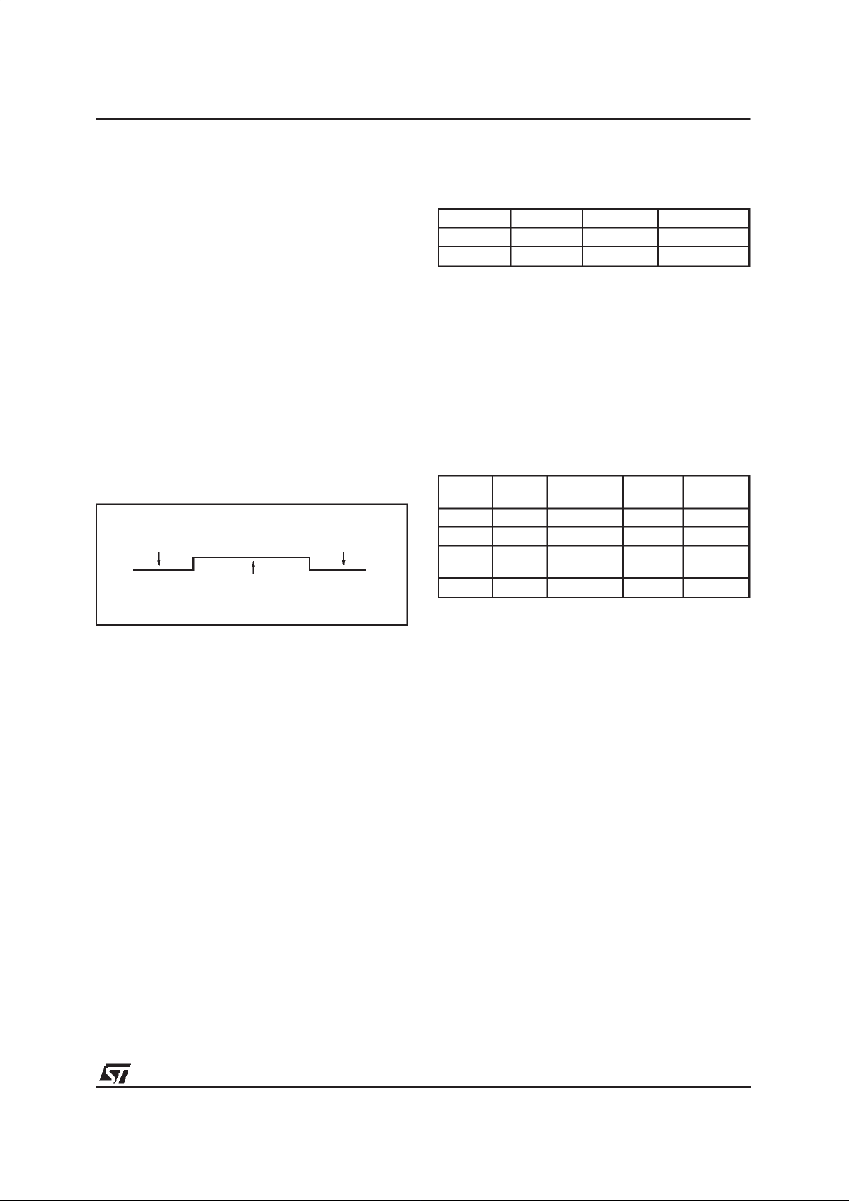
5.4.5. RESET
The Reset min duration (t_reset_low_min)is 100ns
STA013 - STA013B - STA013T
RESET
5.5. CONFIGURATION FLOW
set
set
set
{
set
{
set
HW RESET
PCM-DIVIDER
PCM-CONF.
FRAC_441_H,
PLL
PLL
FRAC_441_L,
PLL
FRAC_H,
PLL FRAC_L }
MFS DF_441,
MFSDF }
PLL CTRL
t
reset_low_min
PCM
OUTPUT
INTERFACE
CONFIGURATION
PLL
CONFIGURATION
FOR:
{
48, 44.1, 32
•
29, 22.05, 16
12, 11.025, 8 } KHz
•
MULTIMEDIA
MODE see
{TAB 5 to TAB12}
OVERALL
THE
SETTING
ARE INCLUDED
THE
CONFIGURATION
FILE AND
BE
IN ONE
STM
A
CONFIGURATION
FILE FOR
SUPPORTED
INPUT
FREQUENCY
STEPS
STA013
CAN
DOWNLOADED
STEP.
PROVIDES
SPECIFIC
EACH
CLOCK
D98AU974
IN
set
SCLK_POL
set
DATA_REQ_ENABLE
set
REQ_POL
set
RUN
INPUT
SERIAL
CLOCK
POLARITY
CONFIGURATION
REQUEST
DATA
PIN ENABLE
REQUEST
DATA
POLARITY
CONFIGURATION
D98AU975
31/38
Page 32

STA013 - STA013B - STA013T
Table 5:
PLL ConfigurationSequenceFor
10MHz Input Clock
256 OversaplingClock
REGISTER
ADDRESS
6 reserved 18
11 reserved 3
97 MFSDF (x) 15
80 MFSDF-441 16
101 PLLFRAC-H 169
82 PLLFRAC-441-H 49
100 PLLFRAC-L 42
81 PLLFRAC-441-L 60
5 PLLCTRL 161
NAME VALUE
Table 6:
PLL ConfigurationSequenceFor
10MHz Input Clock
384 OversaplingRathio
Table 7:
PLL ConfigurationSequence For
14.31818MHzInput Clock
256 OversaplingRathio
REGISTER
ADDRESS
6 reserved 12
11 reserved 3
97 MFSDF (x) 15
80 MFSDF-441 16
101 PLLFRAC-H 187
82 PLLFRAC-441-H 103
100 PLLFRAC-L 58
81 PLLFRAC-441-L 119
5 PLLCTRL 161
NAME VALUE
Table 8:
PLL ConfigurationSequence For
14.31818MHzInput Clock
384 OversaplingRathio
REGISTER
ADDRESS
6 reserved 17
11 reserved 3
97 MFSDF (x) 9
80 MFSDF-441 10
101 PLLFRAC-H 110
82 PLLFRAC-441-H 160
100 PLLFRAC-L 152
81 PLLFRAC-441-L 186
5 PLLCTRL 161
NAME VALUE
REGISTER
ADDRESS
6 reserved 11
11 reserved 3
97 MFSDF (x) 6
80 MFSDF-441 7
101 PLLFRAC-H 3
82 PLLFRAC-441-H 157
100 PLLFRAC-L 211
81 PLLFRAC-441-L 157
5 PLLCTRL 161
NAME VALUE
32/38
Page 33

STA013 - STA013B - STA013T
Table 9:
PLL ConfigurationSequenceFor
14.31818MHzInput Clock
512 OversaplingRathio
REGISTER
ADDRESS
6 reserved 11
11 reserved 3
97 MFSDF (x) 6
80 MFSDF-441 7
101 PLLFRAC-H 3
82 PLLFRAC-441-H 157
100 PLLFRAC-L 211
81 PLLFRAC-441-L 157
5 PLLCTRL 161
NAME VALUE
Table 10:
PLL ConfigurationSequenceFor
14.7456MHz Input Clock
256 OversaplingRathio
Table 11:
PLL ConfigurationSequenceFor
14.7456MHz Input Clock
384 OversaplingRathio
REGISTER
ADDRESS
6 reserved 10
11 reserved 3
97 MFSDF (x) 8
80 MFSDF-441 9
101 PLLFRAC-H 64
82 PLLFRAC-441-H 124
100 PLLFRAC-L 0
81 PLLFRAC-441-L 0
5 PLLCTRL 161
NAME VALUE
Table 12:
PLL ConfigurationSequenceFor
14.7456MHz Input Clock
512 OversaplingRathio
REGISTER
ADDRESS
6 reserved 12
11 reserved 3
97 MFSDF (x) 15
80 MFSDF-441 16
101 PLLFRAC-H 85
82 PLLFRAC-441-H 4
100 PLLFRAC-L 85
81 PLLFRAC-441-L 0
5 PLLCTRL 161
NAME VALUE
REGISTER
ADDRESS
6 reserved 9
11 reserved 2
97 MFSDF (x) 5
80 MFSDF-441 6
101 PLLFRAC-H 0
82 PLLFRAC-441-H 184
100 PLLFRAC-L 0
81 PLLFRAC-441-L 0
5 PLLCTRL 161
NAME VALUE
33/38
Page 34

STA013 - STA013B - STA013T
5.6. STA013CONFIGURATION FILE FORMAT
The STA013 Configuration File is an ASCIIformat. An example of thefile formatis the following:
58 1
42 4
128 15
............
It is a sequenceof rows and each one can be interpretedas an I
The first part of the row is the I
2
C address(register) and the second one is the I2C data (value).
To download the STA013 configuration file into the device, a sequenceof write operationto STA013 I
interfacemust be performed.
The following program describes the I
2
C routineto be implementedfor the configurationdriver:
42 4 I2C REGISTER VALUE
2
I
D98AU976
C SUB-ADDRESS
STA013 Configuration Code (pseudo code)
2
C command.
2
C
download cfg - file
{
fopen (cfg_file);
fp:=1; /*set filepointer to first row */
do
{
2
I
C_start_cond; /* generate I2C startconditionfor STA013deviceaddress*/
2
I
C_write_dev_addr; /*writeSTA013deviceaddress */
2
I
C_write_subaddress(fp); /*writesubaddress */
2
I
C_write_data(fp); /*writedata */
2
I
C_stop_cond; /*generate I2C stopcondition */
fp++; /* update pointer to new file row */
}
while
(!EDF) /* repeatuntilEndof File */
} /* Endroutine */
Note:1
STA013 isa device based onan integratedDSP core. Some ofthe I2C registers default values are loaded after an internal DSP boot operation.
The bootstrap time is 60 micro second. Only after this time lenght, the data in the register can be considered stable.
Note 2:
Refer also to the application note 1090
34/38
Page 35

STA013 - STA013B - STA013T
DIM.
MIN. TYP. MAX. MIN. TYP. MAX.
A 2.65 0.104
a1 0.1 0.3 0.004 0.012
b 0.35 0.49 0.014 0.019
b1 0.23 0.32 0.009 0.013
C 0.5 0.020
c1 45° (typ.)
D 17.7 18.1 0.697 0.713
E 10 10.65 0.394 0.419
e 1.27 0.050
e3 16.51 0.65
F 7.4 7.6 0.291 0.299
L 0.4 1.27 0.016 0.050
S8°(max.)
mm inch
OUTLINE AND
MECHANICAL DATA
SO28
35/38
Page 36

STA013 - STA013B - STA013T
DIM.
mm inch
MIN. TYP. MAX. MIN. TYP. MAX.
A 1.60 0.063
A1 0.05 0.15 0.002 0.006
A2 1.35 1.40 1.45 0.053 0.055 0.057
B 0.30 0.37 0.45 0.012 0.014 0.018
C 0.09 0.20 0.004
0.008
D 12.00 0.472
D1 10.00 0.394
D3 8.00 0.315
e 0.80 0.031
E 12.00 0.472
E1 10.00 0.394
E3 8.00 0.315
L 0.45 0.60 0.75 0.018 0.024 0.030
L1 1.00 0.039
K 0°(min.), 3.5°(typ.), 7°(max.)
OUTLINE AND
MECHANICAL DATA
TQFP44 (10 x 10)
D
D1
A1
2333
34
B
44
1
e
11
TQFP4410
22
E
E1
12
L
0.10mm
.004
Seating Plane
B
K
A
A2
C
36/38
Page 37

STA013 - STA013B - STA013T
mm inch
DIM.
MIN. TYP. MAX. MIN. TYP. MAX.
A 1.700 0.067
A1 0.350 0.400 0.450 0.014 0.016 0.018
A2 1.100 0.043
b 0.500 0.20
D 8.000 0.315
D1 5.600 0.220
e 0.800 0.031
E 8.000 0.315
E1 5.600 0.220
f 1.200 0.047
OUTLINE AND
MECHANICAL DATA
Body: 8 x 8 x 1.7mm
LFBGA64
BALL 1 IDENTIFICATION
D1 D
A
B
C
D
E
F
G
H
φ b (64 PLACES)
f
12345678
f
E1
A2e
0.15
A
A1
E
LFBGA64M
37/38
Page 38

STA013 - STA013B - STA013T
Information furnished is believed to be accurate and reliable. However, STMicroelectronics assumes no responsibility for the consequences
of use of such information nor for any infringement of patents or other rights of third parties which may result from its use. No license is
granted by implication or otherwise under any patent or patent rights of STMicroelectronics. Specification mentioned in this publication are
subject to change without notice. This publication supersedes and replaces all information previously supplied. STMicroelectronics products
are not authorized for use as critical components in life support devices or systems without express written approval of STMicroelectronics.
The ST logo is a registeredtrademark of STMicroelectronics
1999 STMicroelectronics – Printed in Italy – All Rights Reserved
STMicroelectronics GROUP OF COMPANIES
Australia - Brazil - China - Finland - France - Germany - Hong Kong - India - Italy - Japan - Malaysia - Malta - Morocco -
Singapore - Spain - Sweden - Switzerland - United Kingdom - U.S.A.
http://www.st.com
38/38
 Loading...