


e
查询ST72T331N2B3S供应商
ST72E331
ST72T331
8-BIT MCU WITH 8 TO 16K OTP/EPROM, 256 EEPROM,
384 TO 512 BYTES RAM, ADC, WDG, SCI, SPI AND 2 TIMERS
DATASHEET
■ User Program Memory (OTP/EPROM):
8 to 16K byte s
■ User EEPROM: 256 bytes
■ Data RAM: 384 to 512 bytes including 256 bytes
of stack
■ Master Reset and Power-On Reset
■ Low Voltage Detector (LVD) Reset option
■ Run and Power Saving modes
■ 44 or 32 multifunctional bidirectional I/O lines:
PSDIP42
– 15 or 9 programmable interrupt inputs
– 8 or 4 high sink outputs
– 8 or 6 analog alternate inputs
– 13 alternate functions
–EMI filtering
■ Software or Hardware Watchdog (WDG)
■ Two 16-bit Timers, each featuring:
– 2 Input Captures
– 2 Output Compares
– External Clock input (on Timer A)
1)
1)
PSDIP56
– PWM and Pulse Generator modes
■ Synchronous Serial Peripheral Interface (SPI)
■ Asynchronous Serial Communications Interface
(SCI)
■ 8-bit ADC with 8 channels
■ 8-bit Data Manipulation
■ 63 basic Instructions an d 17 main Addressing
Modes
■ 8 x 8 Unsigned Multiply Instruction
■ True Bit Manipulation
■ Complete Development Support on DOS/
WINDOWS
■ Full Software Package on DOS/WINDOWS
TM
Real-Time Emulator
(C-Compiler, Cross-Assembler, Debugger)
2)
TQFP64
(See ordering information at the end of datashe
TM
Notes:
1. One only on Time r A.
2. Six channels only for ST72 T 331J.
Device Summary
Features ST72T33 1J2 ST72T331J4 ST72T331 N2 ST72T331N4
Program Memory - bytes 8K 16K 8K 16K
EEPROM - bytes 256
RAM (stack) - bytes 384 (256) 512 (256) 384 (256) 512 (256)
Peripherals Watchdog, Timers, SPI, SCI, ADC and optional Low Voltage Detector Reset
Operating Supply 3 to 5.5 V
CPU Frequency 8MHz max (16MHz oscillator) - 4MHz max over 85°C
Temperature Range - 40°C to + 125°C
Package TQFP44 - SDIP42 TQFP64 - SDIP56
Note: The ROM versions are supported by the ST72334 family.
May 2001 1/107
CSDIP42W
CSDIP56W
TQFP44
Rev. 1.8
1

Table of Contents
ST72E331
ST72T331 . . . . . . . . . . . . . . . . . . . . . . . . . . . . . . . . . . . . . . . . . . . 1
1 GENERAL DESCRIPTION . . . . . . . . . . . . . . . . . . . . . . . . . . . . . . . . . . . . . . . . . . . . . . . . . . . . . . 5
1.1 INTRODUCTION . . . . . . . . . . . . . . . . . . . . . . . . . . . . . . . . . . . . . . . . . . . . . . . . . . . . . . . . . 5
1.2 PIN DESCRIPTION . . . . . . . . . . . . . . . . . . . . . . . . . . . . . . . . . . . . . . . . . . . . . . . . . . . . . . . 6
1.3 EXTERNAL CONNECTIONS . . . . . . . . . . . . . . . . . . . . . . . . . . . . . . . . . . . . . . . . . . . . . . . 10
1.4 MEMORY MAP . . . . . . . . . . . . . . . . . . . . . . . . . . . . . . . . . . . . . . . . . . . . . . . . . . . . . . . . . 11
1.5 OPTION BYTE . . . . . . . . . . . . . . . . . . . . . . . . . . . . . . . . . . . . . . . . . . . . . . . . . . . . . . . . . . 14
2 CENTRAL PROCESSING UNIT . . . . . . . . . . . . . . . . . . . . . . . . . . . . . . . . . . . . . . . . . . . . . . . . . 15
2.1 INTRODUCTION . . . . . . . . . . . . . . . . . . . . . . . . . . . . . . . . . . . . . . . . . . . . . . . . . . . . . . . . 15
2.2 MAIN FEATURES . . . . . . . . . . . . . . . . . . . . . . . . . . . . . . . . . . . . . . . . . . . . . . . . . . . . . . . 15
2.3 CPU REGISTERS . . . . . . . . . . . . . . . . . . . . . . . . . . . . . . . . . . . . . . . . . . . . . . . . . . . . . . . 15
3 CLOCKS, RESET, INTERRUPTS & POWER SAVING MODES . . . . . . . . . . . . . . . . . . . . . . . . 18
3.1 CLOCK SYSTEM . . . . . . . . . . . . . . . . . . . . . . . . . . . . . . . . . . . . . . . . . . . . . . . . . . . . . . . . 18
3.1.1 General Description . . . . . . . . . . . . . . . . . . . . . . . . . . . . . . . . . . . . . . . . . . . . . . . . . 18
3.1.2 External Clock . . . . . . . . . . . . . . . . . . . . . . . . . . . . . . . . . . . . . . . . . . . . . . . . . . . . . 18
3.2 RESET . . . . . . . . . . . . . . . . . . . . . . . . . . . . . . . . . . . . . . . . . . . . . . . . . . . . . . . . . . . . . . . . 19
3.2.1 Introduction . . . . . . . . . . . . . . . . . . . . . . . . . . . . . . . . . . . . . . . . . . . . . . . . . . . . . . . 19
3.2.2 External Reset . . . . . . . . . . . . . . . . . . . . . . . . . . . . . . . . . . . . . . . . . . . . . . . . . . . . . 19
3.2.3 Reset Operation . . . . . . . . . . . . . . . . . . . . . . . . . . . . . . . . . . . . . . . . . . . . . . . . . . . . 19
3.2.4 Low Voltage Detector Reset . . . . . . . . . . . . . . . . . . . . . . . . . . . . . . . . . . . . . . . . . . 20
4 INTERRUPTS . . . . . . . . . . . . . . . . . . . . . . . . . . . . . . . . . . . . . . . . . . . . . . . . . . . . . . . . . . . . . . . 21
4.1 NON MASKABLE SOFTWARE INTERRUPT . . . . . . . . . . . . . . . . . . . . . . . . . . . . . . . . . . 21
4.2 EXTERNAL INTERRUPTS . . . . . . . . . . . . . . . . . . . . . . . . . . . . . . . . . . . . . . . . . . . . . . . . 21
4.3 PERIPHERAL INTERRUPTS . . . . . . . . . . . . . . . . . . . . . . . . . . . . . . . . . . . . . . . . . . . . . . . 21
4.4 POWER SAVING MODES . . . . . . . . . . . . . . . . . . . . . . . . . . . . . . . . . . . . . . . . . . . . . . . . . 24
4.4.1 Introduction . . . . . . . . . . . . . . . . . . . . . . . . . . . . . . . . . . . . . . . . . . . . . . . . . . . . . . . 24
4.4.2 Slow Mode . . . . . . . . . . . . . . . . . . . . . . . . . . . . . . . . . . . . . . . . . . . . . . . . . . . . . . . . 24
4.4.3 Wait Mode . . . . . . . . . . . . . . . . . . . . . . . . . . . . . . . . . . . . . . . . . . . . . . . . . . . . . . . . 24
4.4.4 Halt Mode . . . . . . . . . . . . . . . . . . . . . . . . . . . . . . . . . . . . . . . . . . . . . . . . . . . . . . . . . 25
4.5 MISCELLANEOUS REGISTER . . . . . . . . . . . . . . . . . . . . . . . . . . . . . . . . . . . . . . . . . . . . . 26
5 ON-CHIP PERIPHERALS . . . . . . . . . . . . . . . . . . . . . . . . . . . . . . . . . . . . . . . . . . . . . . . . . . . . . . 27
5.1 I/O PORTS . . . . . . . . . . . . . . . . . . . . . . . . . . . . . . . . . . . . . . . . . . . . . . . . . . . . . . . . . . . . . 27
5.1.1 Introduction . . . . . . . . . . . . . . . . . . . . . . . . . . . . . . . . . . . . . . . . . . . . . . . . . . . . . . . 27
5.1.2 Functional Description . . . . . . . . . . . . . . . . . . . . . . . . . . . . . . . . . . . . . . . . . . . . . . . 27
5.1.3 I/O Port Implementation . . . . . . . . . . . . . . . . . . . . . . . . . . . . . . . . . . . . . . . . . . . . . . 28
5.1.4 Register Description . . . . . . . . . . . . . . . . . . . . . . . . . . . . . . . . . . . . . . . . . . . . . . . . . 31
5.2 EEPROM (EEP) . . . . . . . . . . . . . . . . . . . . . . . . . . . . . . . . . . . . . . . . . . . . . . . . . . . . . . . . . 33
5.2.1 Introduction . . . . . . . . . . . . . . . . . . . . . . . . . . . . . . . . . . . . . . . . . . . . . . . . . . . . . . . 33
5.2.2 Main Features . . . . . . . . . . . . . . . . . . . . . . . . . . . . . . . . . . . . . . . . . . . . . . . . . . . . . 33
5.2.3 Functional description . . . . . . . . . . . . . . . . . . . . . . . . . . . . . . . . . . . . . . . . . . . . . . . 34
5.2.4 Low Power Modes . . . . . . . . . . . . . . . . . . . . . . . . . . . . . . . . . . . . . . . . . . . . . . . . . . 36
5.2.5 Interrupts . . . . . . . . . . . . . . . . . . . . . . . . . . . . . . . . . . . . . . . . . . . . . . . . . . . . . . . . . 36
5.2.6 Register Description . . . . . . . . . . . . . . . . . . . . . . . . . . . . . . . . . . . . . . . . . . . . . . . . . 36
95
2/107
2

Table of Contents
5.3 WATCHDOG TIMER (WDG) . . . . . . . . . . . . . . . . . . . . . . . . . . . . . . . . . . . . . . . . . . . . . . . 37
5.3.1 Introduction . . . . . . . . . . . . . . . . . . . . . . . . . . . . . . . . . . . . . . . . . . . . . . . . . . . . . . . 37
5.3.2 Main Features . . . . . . . . . . . . . . . . . . . . . . . . . . . . . . . . . . . . . . . . . . . . . . . . . . . . . 37
5.3.3 Functional Description . . . . . . . . . . . . . . . . . . . . . . . . . . . . . . . . . . . . . . . . . . . . . . . 37
5.3.4 Hardware Watchdog Option . . . . . . . . . . . . . . . . . . . . . . . . . . . . . . . . . . . . . . . . . . . 38
5.3.5 Low Power Modes . . . . . . . . . . . . . . . . . . . . . . . . . . . . . . . . . . . . . . . . . . . . . . . . . . 38
5.3.6 Interrupts . . . . . . . . . . . . . . . . . . . . . . . . . . . . . . . . . . . . . . . . . . . . . . . . . . . . . . . . . 38
5.3.7 Register Description . . . . . . . . . . . . . . . . . . . . . . . . . . . . . . . . . . . . . . . . . . . . . . . . . 38
5.4 16-BIT TIMER . . . . . . . . . . . . . . . . . . . . . . . . . . . . . . . . . . . . . . . . . . . . . . . . . . . . . . . . . . 40
5.4.1 Introduction . . . . . . . . . . . . . . . . . . . . . . . . . . . . . . . . . . . . . . . . . . . . . . . . . . . . . . . 40
5.4.2 Main Features . . . . . . . . . . . . . . . . . . . . . . . . . . . . . . . . . . . . . . . . . . . . . . . . . . . . . 40
5.4.3 Functional Description . . . . . . . . . . . . . . . . . . . . . . . . . . . . . . . . . . . . . . . . . . . . . . . 40
5.4.4 Low Power Modes . . . . . . . . . . . . . . . . . . . . . . . . . . . . . . . . . . . . . . . . . . . . . . . . . 52
5.4.5 Interrupts . . . . . . . . . . . . . . . . . . . . . . . . . . . . . . . . . . . . . . . . . . . . . . . . . . . . . . . . . 52
5.4.6 Summary of Timer modes . . . . . . . . . . . . . . . . . . . . . . . . . . . . . . . . . . . . . . . . . . . . 52
5.4.7 Register Description . . . . . . . . . . . . . . . . . . . . . . . . . . . . . . . . . . . . . . . . . . . . . . . . . 53
5.5 SERIAL COMMUNICATIONS INTERFACE (SCI) . . . . . . . . . . . . . . . . . . . . . . . . . . . . . . . 58
5.5.1 Introduction . . . . . . . . . . . . . . . . . . . . . . . . . . . . . . . . . . . . . . . . . . . . . . . . . . . . . . . 58
5.5.2 Main Features . . . . . . . . . . . . . . . . . . . . . . . . . . . . . . . . . . . . . . . . . . . . . . . . . . . . . 58
5.5.3 General Description . . . . . . . . . . . . . . . . . . . . . . . . . . . . . . . . . . . . . . . . . . . . . . . . . 58
5.5.4 Functional Description . . . . . . . . . . . . . . . . . . . . . . . . . . . . . . . . . . . . . . . . . . . . . . . 60
5.5.5 Low Power Modes . . . . . . . . . . . . . . . . . . . . . . . . . . . . . . . . . . . . . . . . . . . . . . . . . . 65
5.5.6 Interrupts . . . . . . . . . . . . . . . . . . . . . . . . . . . . . . . . . . . . . . . . . . . . . . . . . . . . . . . . . 65
5.5.7 Register Description . . . . . . . . . . . . . . . . . . . . . . . . . . . . . . . . . . . . . . . . . . . . . . . . . 66
5.6 SERIAL PERIPHERAL INTERFACE (SPI) . . . . . . . . . . . . . . . . . . . . . . . . . . . . . . . . . . . . 70
5.6.1 Introduction . . . . . . . . . . . . . . . . . . . . . . . . . . . . . . . . . . . . . . . . . . . . . . . . . . . . . . . 70
5.6.2 Main Features . . . . . . . . . . . . . . . . . . . . . . . . . . . . . . . . . . . . . . . . . . . . . . . . . . . . . 70
5.6.3 General description . . . . . . . . . . . . . . . . . . . . . . . . . . . . . . . . . . . . . . . . . . . . . . . . . 70
5.6.4 Functional Description . . . . . . . . . . . . . . . . . . . . . . . . . . . . . . . . . . . . . . . . . . . . . . . 72
5.6.5 Low Power Modes . . . . . . . . . . . . . . . . . . . . . . . . . . . . . . . . . . . . . . . . . . . . . . . . . . 79
5.6.6 Interrupts . . . . . . . . . . . . . . . . . . . . . . . . . . . . . . . . . . . . . . . . . . . . . . . . . . . . . . . . . 79
5.6.7 Register Description . . . . . . . . . . . . . . . . . . . . . . . . . . . . . . . . . . . . . . . . . . . . . . . . . 80
5.7 8-BIT A/D CONVERTER (ADC) . . . . . . . . . . . . . . . . . . . . . . . . . . . . . . . . . . . . . . . . . . . . . 83
5.7.1 Introduction . . . . . . . . . . . . . . . . . . . . . . . . . . . . . . . . . . . . . . . . . . . . . . . . . . . . . . . 83
5.7.2 Main Features . . . . . . . . . . . . . . . . . . . . . . . . . . . . . . . . . . . . . . . . . . . . . . . . . . . . . 83
5.7.3 Functional Description . . . . . . . . . . . . . . . . . . . . . . . . . . . . . . . . . . . . . . . . . . . . . . . 84
5.7.4 Low Power Modes . . . . . . . . . . . . . . . . . . . . . . . . . . . . . . . . . . . . . . . . . . . . . . . . . . 84
5.7.5 Interrupts . . . . . . . . . . . . . . . . . . . . . . . . . . . . . . . . . . . . . . . . . . . . . . . . . . . . . . . . . 84
5.7.6 Register Description . . . . . . . . . . . . . . . . . . . . . . . . . . . . . . . . . . . . . . . . . . . . . . . . . 85
6 INSTRUCTION SET . . . . . . . . . . . . . . . . . . . . . . . . . . . . . . . . . . . . . . . . . . . . . . . . . . . . . . . . . . 86
6.1 ST7 ADDRESSING MODES . . . . . . . . . . . . . . . . . . . . . . . . . . . . . . . . . . . . . . . . . . . . . . . 86
6.1.1 Inherent . . . . . . . . . . . . . . . . . . . . . . . . . . . . . . . . . . . . . . . . . . . . . . . . . . . . . . . . . . 87
6.1.2 Immediate . . . . . . . . . . . . . . . . . . . . . . . . . . . . . . . . . . . . . . . . . . . . . . . . . . . . . . . . 87
6.1.3 Direct . . . . . . . . . . . . . . . . . . . . . . . . . . . . . . . . . . . . . . . . . . . . . . . . . . . . . . . . . . . . 87
6.1.4 Indexed (No Offset, Short, Long) . . . . . . . . . . . . . . . . . . . . . . . . . . . . . . . . . . . . . . . 87
6.1.5 Indirect (Short, Long) . . . . . . . . . . . . . . . . . . . . . . . . . . . . . . . . . . . . . . . . . . . . . . . . 87
6.1.6 Indirect Indexed (Short, Long) . . . . . . . . . . . . . . . . . . . . . . . . . . . . . . . . . . . . . . . . . 88
6.1.7 Relative Mode (Direct, Indirect) . . . . . . . . . . . . . . . . . . . . . . . . . . . . . . . . . . . . . . . . 88
3/107
3

ST72E331 ST72T331
6.2 INSTRUCTION GROUPS . . . . . . . . . . . . . . . . . . . . . . . . . . . . . . . . . . . . . . . . . . . . . . . . . 89
7 ELECTRICAL CHARACTERISTICS . . . . . . . . . . . . . . . . . . . . . . . . . . . . . . . . . . . . . . . . . . . . . . 92
7.1 ABSOLUTE MAXIMUM RATINGS . . . . . . . . . . . . . . . . . . . . . . . . . . . . . . . . . . . . . . . . . . . 92
7.2 RECOMMENDED OPERATING CONDITIONS . . . . . . . . . . . . . . . . . . . . . . . . . . . . . . . . . 93
7.3 RESET CHARACTERISTICS . . . . . . . . . . . . . . . . . . . . . . . . . . . . . . . . . . . . . . . . . . . . . . 94
7.4 OSCILLATOR CHARACTERISTICS . . . . . . . . . . . . . . . . . . . . . . . . . . . . . . . . . . . . . . . . . 94
7.5 DC ELECTRICAL CHARACTERISTICS . . . . . . . . . . . . . . . . . . . . . . . . . . . . . . . . . . . . . . 95
7.6 PERIPHERAL CHARACTERISTICS . . . . . . . . . . . . . . . . . . . . . . . . . . . . . . . . . . . . . . . . . 96
8 GENERAL INFORMATION . . . . . . . . . . . . . . . . . . . . . . . . . . . . . . . . . . . . . . . . . . . . . . . . . . . . 102
8.1 EPROM ERASURE . . . . . . . . . . . . . . . . . . . . . . . . . . . . . . . . . . . . . . . . . . . . . . . . . . . . . 102
8.2 PACKAGE MECHANICAL DATA . . . . . . . . . . . . . . . . . . . . . . . . . . . . . . . . . . . . . . . . . . . 103
8.3 ORDERING INFORMATION . . . . . . . . . . . . . . . . . . . . . . . . . . . . . . . . . . . . . . . . . . . . . . 106
9 SUMMARY OF CHANGES . . . . . . . . . . . . . . . . . . . . . . . . . . . . . . . . . . . . . . . . . . . . . . . . . . . . 107
4/107
4

1 GENERAL DESCRIPTION
1.1 INTRODUCTION
ST72E331 ST72T331
The ST72T331 HCMOS Microcontroller Unit
(MCU) is a member of the ST7 f amily. The de vic e
is based on an industry-standard 8-bit core and
features an enhanced instruction set . The device
is normally operated at a 16 MHz oscillator frequency. Under software control, the ST72T331
may be placed in either Wait, Slow or Halt modes,
thus reducing power consumption. Th e enhance d
instruction set and ad dressing modes afford real
programming potential. In addition to standard
8-bit data management, the ST72T331 features
true bit manipulation, 8x8 unsigned multiplication
and indirect addressing modes on the whole memory. The device includes a lo w consumption and
Figure 1. ST72T331 Block Diagram
Internal
OSCIN
OSCOUT
RESET
OSC
CONTROL
AND L VD
8-BIT CO RE
ALU
PROGRAM
MEMORY
(8 - 16K Bytes)
EEPROM
(256 Bytes)
CLOCK
fast sta r t on - c hip o s c illator, CP U , p r og ra m memo ry (OTP/EPROM versions), EEPROM, RAM, 44
(QFP64 and SDIP56) o r 32 (QFP44 and SD IP42)
I/O lines, a Low V oltage Detector (LVD) and the
following on-chip peripherals: Analog-to-Digital
converter (ADC) with 8 (QFP64, SDIP56) or 6
(QFP44, SDIP42) multiplexed analog inputs, industry standard s ynchronous SPI and asynchronous SCI serial interfaces, digital Watchdog, two
independent 16-bit Timers, one featuring an External Clock Input, and bo th featuring Pulse G enerator capabilities, 2 Input Captures and 2 Output
Compares (only 1 Input Capture and 1 Output
Compare on Timer A).
PORT A
PORT B
TIMER B
ADDRESS AND DATA BUS
PORT C
SPI
PORT D
8-BIT ADC
PA0 - > PA7
(8 bits for ST72T331N)
(5 bits for ST72T331J)
PB0 - > PB7
(8 bits for ST72T331N)
(5 bits for S T 72T331J)
PC0 -> PC7
(8 bits)
PD0 -> PD7
(8 bits for ST72T331N)
(6 bits for S T 72T331J)
PF0 -> PF 2,4,6,7
(6 bits)
V
DD
V
SS
RAM
(384 - 512 Bytes)
PORT F
TIMER A
POWER
SUPPLY
PORT E
SCI
WATCHDOG
PE0 -> PE7
(6 bits for S T 72T 331N)
(2 bits for ST72T331J)
V
DDA
V
SSA
5/107
5

ST72E331 ST72T331
1.2 PIN DESCRI PTION
Figure 2. 64-Pin Thin QFP Package Pinout
1)
PP
DD_2
NCNCPE1/RDI
64636261 60595857 56 555453 52 515049
PE4
1
PE5
2
PE6
3
PE7
4
PB0
(EI2)
5
PB1
(EI2)
6
PB2
(EI2)
7
PB3
(EI2)
8
(EI3)
PB4
9
(EI3)
PB5
10
(EI3)
11
PB6
(EI3)
12
PB7
AIN0/PD0
AIN1/PD1
AIN2/PD2
AIN3/PD3
13
14
15
16
17181920 21222324 29303132
AIN4/PD4
1. VPP on EPROM/OTP only
PE0/TDO
AIN5/PD5
AIN6/PD6
AIN7/PD7
SS_2
V
OSCIN
OSCOUT
V
NCNCRESET
TEST/V
PA7
PA6
PA5
PA4
V
48
SS_1
V
47
DD_1
ICAP1_A/PF6
46
45
44
43
42
41
40
39
38
37
36
35
34
33
EXTCLK_A/PF7
PA3
PA2
PA1
PA0
PC7/SS
PC6/SCK
PC5/MOSI
PC4/MISO
PC3/ICAP1_B
PC2/ICAP2_B
PC1/OCMP1_B
PC0/OCMP2_B
V
SS_0
V
DD_0
(EI0)
(EI0)
(EI0)
(EI0)
(EI1)
(EI1)
(EI1)
25262728
NC
SSA
DDA
V
V
PF1
SS_3
DD_3
V
V
CLKOUT/PF0
NC
PF2
OCMP1_A/PF4
Figure 4. 44-Pin Thin QFP Package Pinout
1)
PP
DD_2
SS_2
V
V
RESET
TEST/V
PA7
PA6
PA5
20 21 22
ICAP1_A/PF 6
EXTCLK_A/PF7
(EI0)
V
PA4
V
33
SS_1
V
32
DD_1
31
PA3
30
PC7/S S
29
PC6/SCK
28
PC5/MOSI
27
PC4/MISO
26
PC3/ICAP 1_ B
25
PC2/ICAP 2_ B
24
PC1/OCMP1 _B
23
PC0/OCMP2 _B
SS_0
DD_0
V
PE0/TD0
PE1/RDI
PB0
PB1
PB2
PB3
PB4
AIN0/PD0
AIN1/PD1
AIN2/PD2
AIN3/PD3
AIN4/PD4
44 43 42 41 40 39 3 8 37 3 6 35 3 4
1
(EI2)
2
(EI2)
3
(EI2)
4
(EI2)
5
(EI3)
6
7
8
9
10
11
12 13 14 15 16 1 7 18 1 9
AIN5/PD5
1. VPP on EPROM/OTP only
V
DDA
V
OSCIN
SSA
OSCOUT
(EI1)
(EI1)
(EI1)
PF1
PF2
CLKOUT/PF 0
OCMP1_A/PF4
Figure 3. 56-Pin Shrink DIP Package Pinout
PB4
PB5
PB6
PB7
AIN0/PD0
AIN1/PD1
AIN2/PD2
AIN3/PD3
AIN4/PD4
AIN5/PD5
AIN6/PD6
AIN7/PD7
V
DDA
V
SSA
CLKOUT/PF0
PF1
OCMP1_A/PF4
EXTCLK_A/PF7
PC0/OCMP2_B
PC1/OCMP1_B
1. VPP on EPROM/OTP only
PF2
ICAP1_A/PF6
V
DD_0
V
SS_0
PC2/ICAP2_B
PC3/ICAP1_B
PC4/MISO
PC5/MOSI
1 (EI3)
2 (EI3)
3 (EI3)
4 (EI3)
5
6
7
8
9
10
11
12
13
14
15 (EI1)
16 (EI1)
17 (EI1)
18
19
20
21
22
23
24
25
26
27
28
(EI2) 56
(EI2) 55
(EI2) 54
(EI2) 53
(EI0) 34
(EI0) 33
(EI0) 32
(EI0) 31
PB3
PB2
PB1
PB0
PE7
52
PE6
51
PE5
50
PE4
49
PE1/RDI
48
PE0/TD0
47
V
46
DD_2
OSCIN
45
OSCOUT
44
V
43
SS_2
42
RESET
1)
TEST/V
41
40
39
38
37
36
35
30
29
PA7
PA6
PA5
PA4
V
SS_1
V
DD_1
PA3
PA2
PA1
PA0
PC7/SS
PC6/SCK
PP
Figure 5. 42-Pin Shrink DIP Package Pinout
PB4
AIN0/PD0
AIN1/PD1
AIN2/PD2
AIN3/PD3
AIN4/PD4
AIN5/PD5
V
DDA
V
SSA
CLKOUT/PF0
PF1
OCMP1_A/PF4
EXTCLK_A/PF7
PC0/OCMP2_B
PC1/OCMP1_B
1. VPP on EPROM/OTP only
PF2
ICAP1_A/PF6
PC2/ICAP2_B
PC3/ICAP1_B
PC4/MISO
PC5/MOSI
1
(EI3)
2
3
4
5
6
7
8
9
10
11
12
13
14
15
16
17
18
19
20
21
(EI1)
(EI1)
(EI1)
(EI2)
(EI2)
(EI2)
(EI2)
(EI0)
42
41
40
39
38
37
36
35
34
33
32
31
30
29
28
27
26
25
24
23
22
PB3
PB2
PB1
PB0
PE1/RDI
PE0/TD0
V
DD_2
OSCIN
OSCOUT
V
SS_2
RESET
TEST/V
PA7
PA6
PA5
PA4
V
SS_1
V
DD_1
PA3
PC7/SS
PC6/SCK
1)
PP
6/107
6

Table 1. ST72T331Nx Pin Description
ST72E331 ST72T331
Pin n°
QFP64
Pin n°
SDIP56
Pin Na m e
Type
Description Remarks
1 49 PE4 I/O Port E4 High Sink
2 50 PE5 I/O Port E5 High Sink
3 51 PE6 I/O Port E6 High Sink
4 52 PE7 I/O Port E7 High Sink
5 53 PB0 I/O Port B0 External Interrupt: EI2
6 54 PB1 I/O Port B1 External Interrupt: EI2
7 55 PB2 I/O Port B2 External Interrupt: EI2
8 56 PB3 I/O Port B3 External Interrupt: EI2
9 1 PB4 I/O Port B4 External Interrupt: EI3
10 2 PB5 I/O Port B5 External Interrupt: EI3
11 3 PB6 I/O Port B6 External Interrupt: EI3
12 4 PB7 I/O Port B7 External Interrupt: EI3
13 5 PD0/AIN0 I/O Port D0 or ADC Analog Input 0
14 6 PD1/AIN1 I/O Port D1 or ADC Analog Input 1
15 7 PD2/AIN2 I/O Port D2 or ADC Analog Input 2
16 8 PD3/AIN3 I/O Port D3 or ADC Analog Input 3
17 9 PD4/AIN4 I/O Port D4 or ADC Analog Input 4
18 10 PD5/AIN5 I/O Port D5 or ADC Analog Input 5
19 11 PD6/AIN6 I/O Port D6 or ADC Analog Input 6
20 12 PD7/AIN7 I/O Port D7 or ADC Analog Input 7
21 13 V
22 14 V
23 V
24 V
DDA
SSA
DD_3
SS_3
S Power Supply for analog peripheral (ADC)
S Ground for analog peripheral (ADC)
S Main power supply
S Ground
25 15 PF0/CLKOUT I/O Port F0 or CPU Clock Output External Interrupt: EI1
26 16 PF1 I/O Port F1 External Interrupt: EI1
27 17 PF2 I/O Port F2 External Interrupt: EI1
28 NC Not Connected
29 18 PF4/OCMP1_A I/O Port F4 or Timer A Output Compare 1
30 NC Not Connected
31 19 PF6/ICAP1_A I/O Port F6 or Timer A Input Capture 1
32 20 PF7/EXTCLK_A I/O Port F7 or External Clock on Timer A
33 21 V
34 22 V
DD_0
SS_0
S Main power supply
S Ground
35 23 PC0/OCMP2_B I/O Port C0 or Timer B Output Compare 2
36 24 PC1/OCMP1_B I/O Port C1 or Timer B Output Compare 1
37 25 PC2/ICAP2_B I/O Port C2 or Timer B Input Capture 2
38 26 PC3/ICAP1_B I/O Port C3 or Timer B Input Capture 1
39 27 PC4/MISO I/O Port C4 or SPI Master In / Slave Out Data
40 28 PC5/MOSI I/O Port C5 or SPI Master Out / Slave In Data
41 29 PC6/SCK I/O Port C6 or SPI Serial Clock
42 30 PC7/SS
I/O Port C7 or SPI Slave Select
43 31 PA0 I/O Port A0 External Interrupt: EI0
7/107
7
ST72E331 ST72T331
Pin n°
QFP64
Pin n°
SDIP56
Pin Na m e
Type
Description Remarks
44 32 PA1 I/O Port A1 External Interrupt: EI0
45 33 PA2 I/O Port A2 External Interrupt: EI0
46 34 PA3 I/O Port A3 External Interrupt: EI0
47 35 V
48 36 V
DD_1
SS_1
S Main power supply
S Ground
49 37 PA4 I/O Port A4 High Sink
50 38 PA5 I/O Port A5 High Sink
51 39 PA6 I/O Port A6 High Sink
52 40 PA7 I/O Port A7 High Sink
53 41 TEST/V
54 42 RESET
PP
1)
S
Test mode pin . In the EPROM programming
mode, this pin acts as the programming voltage
input V
PP.
I/O Bidirectional. Active low. Top priority non maskable interrupt.
This pin must be tied
low in user mode
55 NC Not Connected
56 NC Not Connected
57 43 V
SS_2
58 44 OSCOUT O
59 45 OSCIN I
60 46 V
DD_2
S Ground
Input/Output Oscillator pin. These pins connect a parallel-resonant
crystal, or an external source to the on-chip oscillator.
S Main power supply
61 47 PE0/TDO I/O Port E1 or SCI Transmit Data Out
62 48 PE1/RDI I/O Port E1 or SCI Receive Data In
63 NC Not Connected
64 NC Not Connected
Note 1: VPP on EPROM/OTP only.
Table 2. ST72T331Jx Pin Desc ription
Pin n°
QFP44
Pin n°
SDIP42
Pin Name Type Description Remarks
1 38 PE1/RDI I/O Port E1 or SCI Receive Data In
2 39 PB0 I/O Port B0 External Interrupt: EI2
3 40 PB1 I/O Port B1 External Interrupt: EI2
4 41 PB2 I/O Port B2 External Interrupt: EI2
5 42 PB3 I/O Port B3 External Interrupt: EI2
6 1 PB4 I/O Port B4 External Interrupt: EI3
7 2 PD0/AIN0 I/O Port D0 or ADC Analog Input 0
8 3 PD1/AIN1 I/O Port D1 or ADC Analog Input 1
9 4 PD2/AIN2 I/O Port D2 or ADC Analog Input 2
10 5 PD3/AIN3 I/O Port D3 or ADC Analog Input 3
11 6 PD4/AIN4 I/O Port D4 or ADC Analog Input 4
12 7 PD5/AIN5 I/O Port D5 or ADC Analog Input 5
13 8 V
14 9 V
DDA
SSA
S Pow er Supply for analog perip heral (ADC )
S Ground for analog peripheral (ADC)
15 10 PF0/CLKOUT I/O Port F0 or CPU Clock Output External Interrupt: EI1
16 11 PF1 I/O Port F1 External Interrupt: EI1
17 12 PF2 I/O Port F2 External Interrupt: EI1
8/107
8

ST72E331 ST72T331
Pin n°
QFP44
Pin n°
SDIP42
Pin Name Type Description Remarks
18 13 PF4/OCMP1_A I/O Port F4 or Timer A Output Compare 1
19 14 PF6/ICAP1_A I/O Port F6 or Timer A Input Capture 1
20 15 PF7/EXTCLK_A I/O Port F7 or External Clock on Timer A
21 V
22 V
DD_0
SS_0
S Main power supply
S Ground
23 16 PC0/OCMP2_B I/O Port C0 or Timer B Output Compare 2
24 17 PC1/OCMP1_B I/O Port C1 or Timer B Output Compare 1
25 18 PC2/ICAP2_B I/O Port C2 or Timer B Input Capture 2
26 19 PC3/ICAP1_B I/O Port C3 or Timer B Input Capture 1
27 20 PC4/MISO I/O Port C4 or SPI Master In / Slave Out Data
28 21 PC5/MOSI I/O Port C5 or SPI Master Out / Slave In Data
29 22 PC6/SCK I/O Port C6 or SPI Serial Clock
30 23 PC7/SS
I/O Port C7 or SPI Slave Select
31 24 PA3 I/O Port A3 External Interrupt: EI0
32 25 V
33 26 V
DD_1
SS_1
S Main power supply
S Ground
34 27 PA4 I/O Port A4 High Sink
35 28 PA5 I/O Port A5 High Sink
36 29 PA6 I/O Port A6 High Sink
37 30 PA7 I/O Port A7 High Sink
38 31 TEST/V
PP
1)
39 32 RESET
40 33 V
SS_2
41 34 OSCOUT O
42 35 OSCIN I
43 36 V
DD_2
Test mode pin. In the EPROM programming
S
mode, this pin acts as the programming
voltage input V
PP.
I/O Bidirectional. Active low. Top priority non maskable interrupt.
S Ground
Input/Output Oscillator pin. These pins connect a parallel-resonant
crystal, or an external source to the on-chip oscillator.
S Main power supply
This pin must be tied
low in user mode
44 37 PE0/TDO I/O Port E0 or SCI Transmit Data Out
Note 1: VPP on EPROM/OTP only.
9/107
9

ST72E331 ST72T331
1.3 EXTERNAL CONNECTIONS
The following figure shows the recom mended external connections for the device.
The V
pin is only used for programming OTP
PP
and EPROM devices and must be tied to ground in
user mode.
The 10 nF and 0. 1 µF decoupling capacitors on
the power supply lines are a suggested EMC performance/cost tradeoff.
Figure 6. Recommended Extern al Connec tions
V
DD
Optional if Low Voltage
Detector (LVD) is used
EXTERNAL RESET CIRCUIT
10nF
+
See
A/D Converter
Section
V
DD
0.1µF
0.1µF
The external reset network is intended to protect
the device against parasitic resets, especially in
noisy environments.
Unused I/Os shoul d be t ied hi gh to av oid any unnecessary power consumption on floating lines.
An alternative solution is to program the unused
ports as inputs with pull-up.
V
PP
V
4.7K
DD
V
SS
V
DDA
V
SSA
RESET
0.1µF
10/107
10
See
Clocks
Section
Or configure unused I/O ports
by software as input with pull-up
V
10K
DD
OSCIN
OSCOUT
Unused I/O

1.4 MEMORY MA P
Figure 7. Program Memo ry Map
ST72E331 ST72T331
0000h
007Fh
0080h
01FFh
027Fh
0200h / 0280h
0BFFh
0C00h
0CFFh
0D00h
BFFFh
C000h
E000h
FFDFh
FFE0h
FFFFh
HW Registers
(see Table 4)
384 Bytes RAM
512 Bytes RAM
Reserved
EEPROM256 Bytes
Reserved
16K Bytes
Program
8K Bytes
Memory
Program
Memory
Interrupt & Reset Vectors
(see Table 3)
0080h
Short Addressing
00FFh
0100h
01FFh
0080h
00FFh
0100h
RAM (zero page)
256 Bytes Stack/
16-bit Addressing RAM
Short Addressing
RAM (zero page)
256 Bytes Stack/
16-bit Addressing RAM
01FFh
0200h
027Fh
16-bit Addressing
RAM
Table 3. Interrupt Vector Map
Vector Address Description Remarks
FFE0-FFE1h
FFE2-FFE3h
FFE4-FFE5h
FFE6-FFE7h
FFE8-FFE9h
FFEA-FFEBh
FFEC-FFEDh
FFEE-FFEFh
FFF0-FFF1h
FFF2-FFF3h
FFF4-FFF5h
FFF6-FFF7h
FFF8-FFF9h
FFFA-FFFBh
FFFC-FFFDh
FFFE-FFFFh
EEPROM Interrupt Vector
TIMER B Interrupt Vector
TIMER A Interrupt Vector
External Interrupt Vector EI3
External Interrupt Vector EI2
External Interrupt Vector EI1
External Interrupt Vector EI0
TRAP (software) Interrupt Vector
Not Used
Not Used
SCI Interrupt Vector
SPI interrupt vector
Not Used
Not Used
Not Used
RESET Vector
Internal Interrupt
Internal Interrupt
Internal Interrupt
Internal Interrupt
Internal Interrupt
External Interrupt
External Interrupt
External Interrupt
External Interrupt
CPU Interrupt
11/107
11

ST72E331 ST72T331
Table 4. Hardware Register Mem ory Map
Address Block
0000h
0001h
Port A
0002h
Register
Label
PADR
PADDR
PAOR
Register Name
Data Register
Data Direction Register
Option Register
Reset
Status
00h
00h
00h
Remarks
R/W
R/W
R/W
1)
0003h Reserved Area (1 byte)
0004h
0005h
0006h
Port C
PCDR
PCDDR
PCOR
Data Register
Data Direction Register
Option Register
00h
00h
00h
R/W
R/W
R/W
0007h Reserved Area (1 byte)
0008h
0009h
000Ah
Port B
PBDR
PBDDR
PBOR
Data Register
Data Direction Register
Option Register
00h
00h
00h
R/W
R/W
R/W
1)
000Bh Reserved Area (1 byte)
000Ch
000Dh
000Eh
Port E
PEDR
PEDDR
PEOR
Data Register
Data Direction Register
Option Register
00h
00h
0Ch
R/W
R/W
R/W
1)
000Fh Reserved Area (1 byte)
0010h
0011h
0012h
Port D
PDDR
PDDDR
PDOR
Data Register
Data Direction Register
Option Register
00h
00h
00h
R/W
R/W
R/W
1)
0013h Reserved Area (1 byte)
0014h
0015h
0016h
0017h to
001Fh
Port F
PFDR
PFDDR
PFOR
Data Register
Data Direction Register
Option Register
Reserved Area (9 bytes)
00h
00h
28h
R/W
R/W
R/W
1)
0020h MISCR Miscellaneous Regis ter 00h
0021h
0022h
0023h
0024h to
0029h
002Ah
002Bh
SPI
WDG
SPIDR
SPICR
SPISR
WDGCR
WDGSR
SPI Data I/O Register
SPI Control Register
SPI Status Register
Reserved Area (6 bytes)
Watchdog Control Register
Watchdog Status Register
xxh
xxh
00h
7Fh
00h
R/W
R/W
Read Only
R/W
3)
R/W
002Ch EEPROM EEPCR EEPROM Control Register 00h R/W Register
002Dh to
0030h
Reserved Area (4 bytes)
12/107
12

ST72E331 ST72T331
Address Block
0031h
0032h
0033h
0034h-0035h
0036h-0037h
0038h-0039h
Timer A
003Ah-003Bh
003Ch-003Dh
003Eh-003Fh
Register
Label
TACR2
TACR1
TASR
TAIC1HR
TAIC1LR
TAOC1HR
TAOC1LR
TACHR
TACLR
TAACHR
TAACLR
TAIC2HR
TAIC2LR
TAOC2HR
TAOC2LR
Register Name
Control Register2
Control Register1
Status Register
Input Capture1 High Register
Input Capture1 Low Register
Output Compare1 High Register
Output Compare1 Low Register
Counter High Register
Counter Low Register
Alternate Counter High Register
Alternate Counter Low Register
Input Capture2 High Register
Input Capture2 Low Register
Output Compare2 High Register
Output Compare2 Low Register
Reset
Status
00h
00h
xxh
xxh
xxh
80h
00h
FFh
FCh
FFh
FCh
xxh
xxh
80h
00h
R/W
R/W
Read Only
Read Only
Read Only
R/W
R/W
Read Only
Read Only
Read Only
Read Only
Read Only
Read Only
R/W
R/W
0040h Reserved Area (1 byte)
0041h
0042h
0043h
0044h-0045h
0046h-0047h
0048h-0049h
004Ah-004Bh
004Ch-004Dh
004Eh-004Fh
0050h
0051h
0052h
0053h
0054h
0055h
0056h
0057h
0058h to
006Fh
0070h
0071h
0072h to
007Fh
Timer B
SCI
ADC
TBCR2
TBCR1
TBSR
TBIC1HR
TBIC1LR
TBOC1HR
TBOC1LR
TBCHR
TBCLR
TBACHR
TBACLR
TBIC2HR
TBIC2LR
TBOC2HR
TBOC2LR
SCISR
SCIDR
SCIBRR
SCICR1
SCICR2
SCIERPR
SCIETPR
ADCDR
ADCCSR
Control Register2
Control Register1
Status Register
Input Capture1 High Register
Input Capture1 Low Register
Output Compare1 High Register
Output Compare1 Low Register
Counter High Register
Counter Low Register
Alternate Counter High Register
Alternate Counter Low Register
Input Capture2 High Register
Input Capture2 Low Register
Output Compare2 High Register
Output Compare2 Low Register
SCI Status Register
SCI Data Register
SCI Baud Rate Register
SCI Control Register 1
SCI Control Register 2
SCI Extended Receive Prescaler Register
Reserved
SCI Extended Transmit Prescaler Register
Reserved Area (24 bytes)
ADC Data Register
ADC Control/Status Register
Reserved Area (14 bytes)
00h
00h
xxh
xxh
xxh
80h
00h
FFh
FCh
FFh
FCh
xxh
xxh
80h
00h
C0h
xxh
00x----xb
xxh
00h
00h
---
00h
00h
00h
R/W
R/W
Read Only
Read Only
Read Only
R/W
R/W
Read Only
Read Only
Read Only
Read Only
Read Only
Read Only
R/W
R/W
Read Only
R/W
R/W
R/W
R/W
R/W
Reserved
R/W
Read Only
R/W
Notes:
1. The bits corresponding to unavailable pins are forced to 1 by hardware, this affects the reset status value.
2. External pin not available.
3. Not used in versions without Low Voltage Detector Reset.
Remarks
2)
2)
2)
2)
13/107
13

ST72E331 ST72T331
1.5 OPTION BYTE
The user has the option to select software watchdog or hardware watchdog (see description in the
Watchdog chapter). When program ming EPROM
or OTP devices, this o ption is selected in a men u
by the user of the EPROM programmer before
burning the EPROM/O TP. The Option Byte is located in a non-user map. No address has to be
specified. The Option Byte is at FFh after UV erasure and must be properly programmed t o set desired options.
OPTBYTE
70
- - - - b3 b2 - WDG
Bit 7:4 = Not used
Bit 3 = Reserved, must be cleared.
Bit 2 = Reserved, must be s et on S T7 2T331 N devices and must be cleared on ST72T331J devices.
Bit 1 = Not used
Bit 0 = WDG
Watchdog disable
0: The Watchdog is enabled after reset (Hardware
Watchdog).
1: The Watchdog is not enabled after reset (Soft-
ware Watchdog).
14/107
14

2 CENTRAL PROCE SSI NG UNIT
ST72E331 ST72T331
2.1 INTRODUCTION
This CPU has a full 8-bit architecture and contains
six internal registers allowing efficient 8-bit data
manipulation.
2.2 MAIN FEATURES
■ 63 basic instructions
■ Fast 8-bit by 8-bit multiply
■ 17 main addressing modes
■ Two 8-bit index registers
■ 16-bit stack pointer
■ Low po wer modes
■ Maskable hardware interrupts
■ Non-maskable software interrupt
2.3 CPU REGISTERS
The 6 CPU registers shown in Figure 1 are not
present in the memory mapping and are accessed
by specific instructions.
Figure 8. CPU Registers
70
RESET VALUE = XXh
70
RESET VALUE = XXh
70
RESET VALUE = XXh
Accumulator (A)
The Accumulator is an 8-bit general purpose register used to hold operan ds and the results of the
arithmetic and logic calculations and to manipulate
data.
Index Registers (X and Y)
In indexed addressing modes, these 8-bit registers
are used to create either effective addresses or
temporary storage areas for data manipulation.
(The Cross-Assembler generates a precede instruction (PRE) to indicate that the following instruction refers to the Y register.)
The Y register is not affected by the interrupt automatic procedures (not pushed to and popped from
the stack).
Program Cou nt er (P C )
The program counter is a 16-bit register containing
the address of the next instruction to be executed
by the CPU. It is made of two 8-bit registers PCL
(Program Counter Low which is the LSB) and PCH
(Program Counter High which is the MSB).
ACCUMULA T OR
X INDEX REGISTER
Y INDEX REGISTER
15 8
RESET VALUE = RESET VECTOR @ FFFEh-FFFFh
15
RESET VALUE = STACK HIGHER ADDRESS
PCH
RESET VALUE =
7
70
1C11HI NZ
1X11X1XX
70
8
PCL
0
PROGRAM COUNTER
CONDITION CODE REGISTER
STACK POINTER
X = Undefined Value
15/107
15

ST72E331 ST72T331
CPU REGISTERS (Cont’d)
CONDITION CODE REGISTER (CC)
Read/Write
Reset Value: 111x1xxx
70
111HINZC
The 8-bit Condition Code register c ontains the interrupt mask and four flags represent ative of the
result of the instruction just executed. This register
can also be handled by the PUSH and POP instructions.
These bits can be individually tested and/or controlled by specific instructions.
Bit 4 = H
Half carry
.
This bit is set by hardware when a carry occurs between bits 3 and 4 of t he ALU during an ADD or
ADC instruction. It is reset by hardware during the
same instructions.
0: No half carry has occurred.
1: A half carry has occurred.
This bit is tested using the JRH or JRNH instruction. The H bit is useful in BCD arithmetic subroutines .
Bit 3 = I
Interrupt mask
.
This bit is set by hardware when entering in interrupt or by software to disable all interrup ts except
the TRAP software interrupt. This bit is cleared by
software.
0: Interrupts are enabled.
1: Interrupts are disabled.
This bit is controlled by the RIM, SIM and IRET instructions and is tested by the JRM and JRNM instructions.
Note: Interrupts requested while I is set are
latched and can be processed whe n I is cleared.
By default an interrupt routine is not in terruptable
because the I bi t is set by hardware at the start of
the routine and reset by the IRET instruction at the
end of the routine. If the I bit is cleared by software
in the interrupt routine, pending interrupts are
serviced regardless of the priority level of the current interrupt routine.
Bit 2 = N
Negative
.
This bit is set and cleared by hardware. It is representative of the result sign of the last arithmeti c,
logical or data manipulation. It is a copy of the 7
bit of the result.
0: The result of the last operation is positive or null.
1: The result of the last operation is negative
(i.e. the most significant bit is a logic 1).
This bit is accessed by the JRMI and JRPL instructions.
Zero
Bit 1 = Z
.
This bit is set and cleared by hardware. This bit indicates that the result of the last arithmetic, logical
or data manipulation is zero.
0: The result of the last operation is different from
zero.
1: The result of the last operation is zero.
This bit is accessed by the JREQ and JRNE test
instructions.
Bit 0 = C
Carry/borrow.
This bit is set and cleared b y hardware and software. It indicates an overflow or an underflow has
occurred during the last arithmetic operation.
0: No overflow or underflow has occurred.
1: An overflow or underflow has occurred.
This bit is driven by the SCF and RCF instructions
and tested by the JRC and JRNC instructions. It is
also affected by the “bit test and branch”, shift and
rotate instructions.
th
16/107
16

ST72E331 ST72T331
CENTRAL PROCESSING UNIT (Cont’d)
Stack Pointer (SP)
Read/Write
Reset Value: 01FFh
15 8
00000001
70
SP7 SP6 SP5 SP4 SP3 SP2 SP1 SP0
The Stack Pointer is a 16-bit register which is always pointing to the next free location in the stack.
It is then decremented after data has been pushed
onto the stack and incremented before data is
popped from the stack (see Figure 9).
Since the stack is 256 bytes deep, the 8th most
significant bits are forced by hardware. Following
an MCU Reset, or after a Reset Stack Pointer instruction (RSP), the Stack Pointer contains its reset value (the SP7 to SP0 bits are set) which is the
stack higher address.
The least significant byte of the Stack Pointer
(called S) can be directly accessed by a LD instruction.
Note: When the lower limit is exceeded, the Stack
Pointer wraps around to the stack upper limit, wi thout indicating the s tack overflow. The prev iously
stored information is then o verwritten and therefore lost. The stack also wraps in case of an underflow.
The stack is used to save the retu rn address during a subroutine call and the CPU context during
an interrupt. The user may also directly manipulate
the stack by means of the PUSH and POP instructions. In the case of an interrupt, the PCL is stored
at the first location point ed to by the SP. Then the
other registers are stored in the next locations as
shown in Figure 9.
– When an interrupt is received, the SP is decre-
mented and the context is pushed on the stack.
– On return from interrupt, the SP is incremented
and the context is popped from the stack.
A subroutine call occupies two locations and an interrupt five locat ions i n the sta ck ar ea.
Figure 9. Stack Manipulation Example
@ 0100h
SP
@ 01FFh
CALL
Subroutine
SP
PCH
PCL
Stack Higher Address = 01FFh
Stack Lower Address =
Interrupt
Event
SP
CC
A
X
PCH
PCL
PCH
PCL
0100h
PUSH Y POP Y IRET
SP
Y
CC
A
X
PCH
PCL
PCH
PCL
CC
A
X
PCH
PCL
PCH
PCL
SP
PCH
PCL
RET
or RSP
SP
17/107
17

ST72E331 ST72T331
3 CLOCKS, RESET, INTERRUPTS & POWER SAVI NG MODES
3.1 CLOCK SYSTEM
3.1.1 General Description
The MCU accepts either a crystal or ceramic resonator, or an external clock signal to drive the internal oscillator. The internal clock (f
from the external oscillator frequency (f
) is derived
CPU
OSC).
The
external Oscillator clock is first divided by 2, and
an additional division factor of 2, 4, 8, or 16 can be
applied, in Slow Mode, to red uce th e f requency of
the f
; this clock signal is also routed to the on-
CPU
chip peripherals. The CPU clock signal consists of
a square wave with a duty cycle of 50%.
The internal oscillat or is designed to operate with
an AT-cut parallel resonant quartz crystal resonator in the frequency range specified for f
osc
. The
circuit shown in Fi gure 11 is recommended whe n
using a crystal, and Tab le 5 lists the recommended capacitance and feedback resistance values.
The crystal and associated components should be
mounted as close as p ossible to the input pins i n
order to minimize output distortion and start-up
stabilisation time.
Use of an external CMOS oscillator is recommended when crystals outside the specified frequency ranges are to be used.
3.1.2 External Clock
An external clock may be applied to the OSCIN input with the OSCOUT pin not connected, as
shown on Figure 10.
Figure 10. External Clock Source Connections
OSCIN OSCOUT
NC
EXTERNAL
CLOCK
Figure 11. Crystal/Ceramic Resonator
OSCOUT
C
OSCOUT
C
OSCIN
OSCIN
Table 5 Recommended Values for 16 MHz
R
SMAX
Crystal Resonator (C
R
SMAX
C
OSCIN
C
OSCOUT
40
Ω
56pF 47pF 22pF
56pF 47pF 22pF
: Parasitic series resistance of the quartz
60
< 7pF)
0
Ω
150
Ω
crystal (upper limit).
: Parasitic shunt capacitance of the quartz crys-
C
0
tal (upper limit 7pF).
C
OSCOUT
, C
: Maximum total capacitance on
OSCIN
pins OSCIN and OSCOUT (the value includes the
external capacitance tied to the p in plus the parasitic capacitance of the board and of the device).
18/107
18
Figure 12. Clock Prescaler Block Diagram
C
OSCIN
OSCIN
OSCOUT
%2 % 2, 4, 8, 16
C
OSCOUT
f
CPU
to CPU and
Peripherals

3.2 RESET
ST72E331 ST72T331
3.2.1 Introd uct i on
There are four sources of Reset:
– RESET
pin (external source)
– Power-On Reset (Internal source)
– WATCHDOG (Internal Source)
– Low Voltage Detection Reset (internal source)
The Reset Service Routine vector is located at ad-
dress FFFEh-FFFFh.
3.2.2 External Reset
The RESET
pin is both an input and an open-drain
output with integrated pull-up resi stor. When one
of the internal Reset sources is active, the Reset
pin is driven low for a duration of t
RESET
to reset
the whole application.
3.2.3 Reset Operation
The duration of the Reset state is a minimum of
4096 internal CPU Clock cycles. During the Reset
state, all I/Os take their reset value.
A Reset signal originating from an external source
must have a duration of at least t
PULSE
in order to
Figure 13. Reset Block Diagram
be recognised. This detection is asynchronous
and therefore the MCU can enter Reset state even
in Halt mode.
At the end of the Reset cycle, the MCU may be
held in the Reset state by an External Reset signal. The RESET
has risen to a point where the MCU can oper-
V
DD
pin may thus be used to ens ure
ate correctly before the user program is run. Following a Reset event, or after exiting Halt mode, a
4096 CPU Clock cycle delay period is initiated in
order to allow the oscillat or to stabilise and to ensure that recovery has taken place from the Reset
state.
In the high state, the RESET
ternally to a pull-up resistor (R
pin is connected in-
). This resistor
ON
can be pulled low b y ex ternal circuitry to res et t he
device.
The RESET
pin is an asynchronous signal which
plays a major role in EMS performance. In a noisy
environment, it is rec ommended to u se the external connections shown in Figure 6.
RESET
OSCILLATOR
SIGNAL
V
DD
R
ON
TO ST7
RESET
INTERN AL
RESET
COUNTER
POWER-ON RESE T
WATCHDOG RESET
LOW VOLTAGE DETECTOR RESET
19/107
19

ST72E331 ST72T331
RESET (Cont’d)
3.2.4 Low Voltage Detector Reset
The on-chip Low Voltage Detector (LVD) generates a static reset when the supply voltage is below a reference value. The LVD functions both
during power-on as well as when the power supply
drops (brown-out). The reference value for a voltage drop is lower than the reference value for power-on in order to avoid a parasitic reset when the
MCU starts running and sinks current on the supply (hysteresis).
The LVD Reset circuitry generates a reset when
is below:
V
DD
V
V
Provided the minimun V
the oscillator frequency) is above V
MCU can only be in two modes:
- under full software control or
- in static safe reset
In this condition, secure operation is always en-
sured for the application without the need for external reset hardware.
During a Low Voltage Detector Reset, the RESET
pin is held low, thus perm itting the MCU to reset
other devices.
In noisy environments, the power supply may drop
for short periods and cause the Low Voltage Detector to generate a Reset too frequen tly. In such
when VDD is rising
LVDUP
LVDDOWN
when VDD is falling
value (guaranteed for
DD
LVDDOWN
, the
cases, it is recommended to us e devices without
the LVD Reset option and to rely on the watchdog
function to detect application runaway conditions.
Figure 14. Low Voltage Detector Reset Function
V
DD
LOW VOLTAGE
DETECTOR RESET
FROM
WATCHDOG
RESET
RESET
Figure 15. Low Voltage Detector Reset Signal
V
V
DD
RESET
LVDUP
V
LVDDOWN
Note: See electrical characteristics for values of
LVDUP
and V
LVDDOWN
V
Figure 16. Temporization timing diagram after an internal Reset
V
LVDUP
Temporiz ation (40 96 CP U clock cy cl es)
$FFFE
20/107
V
DD
Addresses
20

4 INTE RRUPTS
ST72E331 ST72T331
The ST7 core may be interrupted by one of two different methods: maskable hardware interrupts as
listed in the Interrupt Mapping Table and a nonmaskable software interrupt (TRAP). The Interrupt
processing flowchart is shown in Figure 1.
The maskable interrupts must be enabled by
clearing the I bit in order to be serviced. However,
disabled interrupts may be latched and processed
when they are enabled (see external interrupts
subsection).
Note: After reset, all interrupts are disabled.
When an interrupt has to be serviced:
– No rmal processing is susp ended at the end of
the current instruction execution.
– The PC, X, A and CC registers are saved onto
the stack.
– The I bit of the CC register is set to prevent addi-
tional interrupts.
– The PC is then loaded with the interrupt vector of
the interrupt to service and the first instruction of
the interrupt service routine is fetched (refer to
the Interrupt Mapping Table for vector addresses).
The interrupt service routine should finish with the
IRET instruction which c auses the conten ts o f the
saved registers to be recovered from the stack.
Note: As a consequence of the IRET instruction,
the I bit will be cleared a nd the main pro gram will
resume.
Priority Management
By default, a servicing interrupt cannot be interrupted because the I bit is set by hardware entering in interrupt routine.
In the case when several inte rrupt s ar e simultaneously pending, an hardware priority defines which
one will be serviced first (see the Interrupt Mapping Table).
Interrupts and Low Power Mode
All interrupts allow the processor to leave the
WAIT low power mode. Only external and specifically mentioned interrupts allow the proc essor to
leave the HALT low power mode (refer to the “Exit
from HALT“ column in the I nterrupt Mapping Table).
4.1 NON MASKABLE SOFTWARE INTERRUPT
This interrupt is entered when the TRAP instruction is executed regardless of the state of the I bit.
It will be serviced according to the flowchart on
Figure 1.
4.2 EXTERNAL INTERRUPTS
External interrupt vectors can be loaded into the
PC register if the corresponding ext ernal interrupt
occurred and if the I bit is cleared. These interrupts
allow the processor to leave the Halt low power
mode.
The external interrupt polarity is selected through
the miscellaneous register or interrupt register (if
available).
An external interrupt triggered on edge will be
latched and the interrupt request automatically
cleared upon entering the interrupt service routine.
If several input pins, connected to the same interrupt vector, are configured as interrupts, their signals are logically ANDed and inverted before entering the edge/level detection block.
Caution: The type of sensitivity defined in the Miscellaneous or Interrupt register (if available) applies to the ei source. In case of an ANDed source
(as described on the I/O ports section), a low level
on an I/O pin configured as input with interrupt,
masks the interrupt request even in case of risingedge sensitivity.
4.3 PERIPHERAL INTERRUPTS
Different peripheral interrupt flags in the status
register are able to cause an interrupt when they
are active if both:
– The I bit of the CC register is cleared.
– The corresponding enable bit is set in the control
register.
If any of these two conditions is false, the interrupt
is latched and thus remains pending.
Clearing an interrupt request is done by:
– Writing “0” to the corresponding bit in the status
register or
– Access to the status register while the f lag i s set
followed by a read or write of an associated register.
Note: the clearing sequence resets the internal
latch. A pending interrupt (i.e. waiting for being enabled) will therefore be lost if the clear sequence is
executed.
21/107
21

ST72E331 ST72T331
INTERRUPTS (Cont’d)
Figure 17. Inte rru pt P rocessing Flow c hart
FROM RESET
EXECUTE INSTRUCTION
RESTORE PC, X, A, CC FROM STACK
I BIT SET?
Y
FETCH NEXT INSTRUCTION
N
THIS CLEARS I BIT BY DEFAULT
IRET?
Y
N
N
INTER RUPT
PENDING?
Y
STACK PC, X, A, CC
SET I BIT
LOAD PC FROM INTERRUPT VECTOR
22/107
22

ST72E331 ST72T331
Table 6. Int errupt Mapp in g
Source
Block
RESET Reset N/A N/A yes F FFEh-FFFFh
TRAP So ftware N/A N/A no FFFCh-FFFDh
EI0 Ext. Interrupt (Ports PA0:PA3) N/A N/A
EI1 Ext. Interrupt (Ports PF0:PF2) N/A N/A FFF4h-FFF5h
EI2 Ext. Interrupt (Ports PB0:PB3) N/A N/A FFF2h-FFF3h
EI3 Ext. Interrupt (Ports PB4:PB7) N/A N/A FFF0h-FFF1h
SPI
TIMER A
TIMER B
SCI
EEPROM EEPROM End of Programming EEPCR E2ITE FFE4h-FFE5h
Transfer Complete
Mode Fault MODF
Input Capture 1
Output Compare 1 OCF1_A
Input Capture 2 ICF2_A
Output Compare 2 OCF2_A
Timer Overflow TOF_A
Input Capture 1
Output Compare 1 OCF1_B
Input Capture 2 ICF2_B
Output Compare 2 OCF2_B
Timer Overflow TOF_B
Transmit Buffer Empty
Transmit Complete TC
Receive Buffer Full RDRF
Idle Line Detect IDLE
Overrun OR
Description
NOT USED FFFAh-FFFBh
NOT USED FFF8h-FFF9h
NOT USED FFEEh-FFEFh
NOT USED FFE2h-FFE3h
NOT USED FFE0h-FFE1h
Register
Label
SPISR
TASR
TBSR
SCISR
Flag
SPIF
ICF1_A
ICF1_B
TDRE
Exit
from
HALT
yes
no
Vector
Address
FFF6h-FFF7h
FFECh-FFEDh
FFEAh-FFEBh
FFE8h-FFE9h
FFE6h-FFE7h
Priority
Order
Highest
Priority
Lowest
Priority
23/107
23

ST72E331 ST72T331
4.4 POWER SAVING MODES
4.4.1 Introd uct i on
There are three Power Saving modes. Slow Mode
is selected by setting the rele vant bits in the Miscellaneous register. Wait and Halt m odes may b e
entered using the WFI and HALT instructions.
Figure 18. WAIT Flow Chart
WFI INSTRUCTION
4.4.2 Slow Mode
In Slow mode, the oscillator frequency can be d ivided by a value defined in the Miscellaneous
Register. The CPU and peripherals are clocked at
this lower frequency. Slow mode is used to reduce
power consumption, and enables the user to adapt
clock frequency to available supply voltage.
4.4.3 Wait Mode
Wait mode places the M CU in a low power consumption mode by stopping the CPU. All peripherals remain active. During Wait mode, th e I bit (CC
Register) is cleared, so as to enable all interrupts.
All other registers and memory remain unchanged.
The MCU w ill remain in Wait mode u ntil an Inte rrupt or Reset occurs, whereupon the Program
Counter branches to the starting address of the Interrupt or Reset Service Routine.
The MCU will remain in Wait mode until a Reset or
an Interrupt occurs, causing it to wake up.
Refer to Figure 18 below.
N
INTERRUPT
Y
OSCILLATOR
PERIPH. CLOCK
CPU CLOCK
I-BIT
N
RESET
OSCILLATOR
PERIPH. CLOCK
CPU CLOCK
I-BIT
4096 CPU CLOCK
CYCLES DELAY
ON
ON
OFF
CLEARED
Y
ON
ON
ON
SET
24/107
24
OSCILLATOR
PERIPH. CLOCK
CPU CLOCK
I-BIT
FETCH RESET VECTOR
OR SERVICE INTERRUP T
Note: Before servicing an interrupt, the CC register is
pushed on the sta ck. The I-Bit is s et d uring the inte rrupt routine and cleared when the CC register is
popped.
ON
ON
ON
SET

POWER SAVING MODES (Cont’d)
4.4.4 Halt Mode
The Halt mode is the MCU lowest power consumption mode. The Halt mode is entered by executing the HALT instruction. The internal oscillator
is then turned off, causing all internal processing to
be stopped, including the operation of the on-chip
peripherals. The Halt mode cannot be used whe n
the watchdog is enabled, if the HALT instruction is
executed while the watchdog system is enabled, a
watchdog reset is generated thus resetting the entire MCU.
When entering Halt mode, the I bit in the CC Register is cleared so as to enable External Interrupts.
If an interrupt occurs, the CPU becomes active.
The MCU can exit the Halt mode upon reception of
an interrupt or a reset. Refer t o the I nterrupt M apping Table. The oscillator is then turned on and a
stabilization time is provided before releasing CPU
operation. The stabilization time is 4096 CPU clock
cycles.
After the start up delay, the CPU continues operation by servicing the interrupt which wakes it up or
by fetching the reset vector if a reset wakes it up.
ST72E331 ST72T331
Figure 19. HALT Flow Chart
HALT INSTRUCTION
WATCHDOG
RESET
N
EXTERNAL
INTERRUPT
Y
OSCILLATOR
PERIPH. CLOCK
CPU CLOCK
I-BIT
N
1)
WDG
ENABLED?
N
OFF
OFF
OFF
CLEARED
RESET
Y
Y
1) or some specific interrupts
2) if reset PERIPH. CLOCK = ON ; if interrupt
PERIPH. CLOCK = OFF
Note: Before servicing an interrupt, the CC register is
pushed on th e sta ck. The I-Bit is s et d uring the inte rrupt routine and cleared when the CC register is
popped.
OSCILLATOR
PERIPH. CLOCK
CPU CLOCK
I-BIT
4096 CPU CLOCK
CYCLES DELAY
OSCILLATOR
PERIPH. CLOCK
CPU CLOCK
I-BIT
FETCH RESET VECTOR
OR SERVICE INTERRUPT
ON
2)
OFF
ON
SET
ON
ON
ON
SET
25/107
25

ST72E331 ST72T331
4.5 MISCELLANEOUS REGISTER
The Miscellaneous register allows to select the
SLOW operating mode , the polarity of ex ternal i nterrupt requests and to output the internal clock.
Register Address: 0020h — Read/Write
Reset Value: 0000 0000 (00h)
70
PEI3 PEI2 MCO PEI1 PEI0 PSM1 PSM0 SMS
Bit 7:6 = PEI[3:2]
Polarity Options
External Interrupt EI3 a nd EI2
.
These bits are set and cleared by software. They
determine which event on EI2 and EI3 causes the
Bit 4:3 = PEI[1:0]
Polarity Opti o n s
These bits are set and cleared by so ftware. They
determine which event on EI0 and EI1 causes the
external interrupt according to Table 8.
Table 8. EI0 and E I1 External Inte rrup t P o larity
Options
Falling edge and low level
(Reset state)
Falling edge only 1 0
Rising edge only 0 1
Rising and falling edge 1 1
External Interrupt EI1 and EI0
.
MODE PEI1 PEI0
external interrupt according to Table 7.
Table 7. EI2 and EI3 External Interrupt Polarity
Options
Note: Any modification of one of these two bits re-
sets the interrupt request related to t his interrupt
vector.
MODE PEI3 PEI2
Falling edge and low level
(Reset state)
Falling edge only 1 0
Rising edge only 0 1
Rising and falling edge 1 1
Note: Any modification of one of these two bits resets the interrupt request related to this interrupt
vect or.
Bit 5 = MCO
Main Clock Out
This bit is set and cleared by software. When set, it
00
Bit 2:1 = PSM[1:0]
Prescaler for Slow Mode
These bits are set and cleared by so ftware. They
determine the CPU clock when the SMS bit is set
according to the following table.
Table 9. f
Value in Slow Mode
CPU
f
Valu e
CPU
/ 4 0 0
f
OSC
/ 16 0 1
f
OSC
/ 8 1 0
f
OSC
f
/ 32 1 1
OSC
enables the output of the Internal Clock on the
PPF0 I/O port.
0 - PF0 is a general purpose I/O port.
1 - MCO alternate function (f
is output on PF0
CPU
pin).
Bit 0 = SMS
This bit is set and cleared by software.
0: Normal Mode - f
Slow Mode Select
= f
CPU
OSC
/ 2
(Reset state)
1: Slow Mode - the f
PSM[1:0] bits .
value is determined by the
CPU
00
PSM1 PSM0
26/107
26

5 ON-CHIP PERIPHERALS
5.1 I/O PORTS
5.1.1 Introd uction
The I/O ports offer different functional modes:
– transfer of data through digital inputs and outputs
and for specific pins:
– an alog signal input (ADC)
– alterna te signal input/output for the on-chip pe-
ripherals.
– external interrupt generat ion
An I/O port is composed of up to 8 pins. Each pin
can be programmed independently as digital input
(with or without interrupt generation) or digital output.
5.1.2 Functional Description
Each port is associated to 2 main registers:
– Data Register (DR)
– Data Direction Register (DDR)
and some of them to an optional register:
– Option Register (OR)
Each I/O pin may be programmed using the corre-
sponding register bits in DDR and OR registers: bit
X corresponding to pin X of the port. The same correspondence is used for the DR register.
The following description takes into account the
OR register, for specific ports which do not provide
this register refer to the I/O Port Implementation
Section 4.1.3. The generic I/O block diagram is
shown on Figure 21.
5.1.2.1 Input Modes
The input configuration is sele cted by clearing the
corresponding DDR register bit.
In this case, reading the DR register returns the
digital value applied to the external I/O pin.
Different input modes can be selected by software
through the OR register.
Notes:
1. All the inputs are triggered by a Schmitt trigger.
2. When switching from input mode to output
mode, the DR register should be written first to
output the correct value as soon as the port is configured as an output.
ST72E331 ST72T331
Interrupt function
When an I/O is configured in Input with Interrupt,
an event on thi s I/O can generat e an external Interrupt request to the CPU. The interrupt polarity is
given independently according to the description
mentioned in the Miscellaneous regi ster or in the
interrupt register (where available).
Each pin can independently generate an Interrupt
request.
Each external interrupt vector is linked t o a dedicated group of I/O port pins (see Interrupts section). If several input pins are configured as inputs
to the same interrupt vector, their sign als are logically ANDed before entering the edge/level detection block. For this reason if one of the interrupt
pins is tied low, it masks the other ones.
5.1.2.2 Output Mode
The pin is configured in output mode by setting the
corresponding DDR register bit.
In this mode, writing “0” or “1” to the DR register
applies this digital value to the I/O pin through the
latch. Then reading the DR register returns the
previously stored value.
Note: In this mode, the interrupt function is disabled.
5.1.2.3 Digital Alternate Function
When an on-chip peripheral is configured to use a
pin, the alternate function is au tomatically selected. This alternate function takes priority over
standard I/O programming. When the signal is
coming from an on-chip peripheral, the I/O pin is
automatically configured in output mode (push-pull
or open drain according to the peripheral).
When the signal is goi ng to an on-chip peripheral,
the I/O pin ha s to be configured in i nput mode. In
this case, the pin’s state is a lso digitally readable
by addressing the DR register.
Notes:
1. Input pull-up configuration can cause an unex pected value at the input of the alternate peripheral input.
2. When the on-chip peripheral uses a pin as input
and output, this pin must be configured as an input
(DDR = 0).
Warning
vated as long as the pin is configured as input with
interrupt, in order to avoid generating spurious interrupts.
: The alternate func tion m us t not be a cti-
27/107
27

ST72E331 ST72T331
I/O PORTS (Cont’d)
5.1.2.4 Analog Alternate Function
When the pin is used as an ADC input the I/O must
be configured as input, floating. The analog multiplexer (controlled by the ADC registers) switches
the analog voltage present o n the selected pin to
the common ana log rail which i s c onnect ed to the
ADC input.
It is recommended not to change the voltage level
or loading on any port pin while conversion is in
progress. Furthermore it i s recommended not to
have clocking pins located close t o a sele cted analog pin.
Warning
within the limits stated in the Absolute M aximum
Ratings.
Figure 20. Recommended I/O State Transition Diagram
: The analog input voltage level mus t be
5.1.3 I/O Port Implementation
The hardware implementation on each I/O port depends on the settings in the DDR and OR registers
and specific feature of the I/O port such as ADC Input (see Figure 21) or true open drain. Switching
these I/O ports from one state to an other should
be done in a sequence that prevents unwanted
side effects. Recommended safe transitions are illustrated in Figure 20. Other transitions are potentially risky and should be avoided, since they are
likely to present unwanted side-effects such as
spurious interrupt generation.
INPUT
with interrupt
INPUT
no interrupt
OUTPUT
open-drain
OUTPUT
push-pull
28/107
28

I/O PORTS (Cont’d)
ST72E331 ST72T331
Figure 21
. I/O Block Diagram
COMMON ANALOG RAIL
ALTERNATE INPUT
LATCH
DDR
LATCH
DATA BUS
LATCH
(SEE TABLE BELOW)
OR SEL
DDR SEL
DR SEL
ALTERNATE
OUTPUT
DR
OR
ALTERNATE ENABLE
1
M
U
X
0
ALTERNATE
1
M
U
X
0
ENABLE
ALTERNATE
ENABLE
PULL-UP
CONDITION
ANALOG ENABLE
(ADC)
(S
EE NOTE BELOW)
PULL-UP
ANALOG
SWITCH
V
DD
P-BUFFER
EE TABLE BELOW)
(S
V
DD
DIODE
(SEE TABLE BELOW)
GND
N-BUFFER
GND
PAD
CMOS
SCHMITT TRIGGER
EXTERNAL
INTERRUPT
SOURCE (EIx)
POLARITY
SEL
FROM
OTHER
BITS
Table 10. Port Mode Configuration
Configuration Mode Pull-up P-buffer VDD Diode
Floating 0 0 1
Pull-up 1 0 1
Push-pull 0 1 1
True Open Drain not present not present not present
Open Drain (logic level) 0 0 1
Legend:
0 - present, not activated
1 - present and activated
Notes:
– No OR Register on some ports (see register map).
– ADC Switch on ports with analog alternate functions.
29/107
29

ST72E331 ST72T331
I/O PORTS (Cont’d)
Table 11. Port Configuration
Port Pin name
PA0:PA2
Port A
PA3 floating* pull-up with interrupt open-drain push-pull
1)
Input (DDR = 0) Output (DDR = 1)
OR = 0 OR = 1 OR = 0 OR =1
floating* pull-up with interrupt open-drain push-pull
PA4:PA7 floating* open drain, high sink capability
PB0:PB4 floating* pull-up with interrupt open-drain
Port B
PB5:PB7
1)
floating* pull-up with interrupt open-drain
Port C PC0:PC7 floating* pull-up open-drain push-pull
PD0:PD5 floating* pull-up open-drain push-pull
Port D
PD6:PD7
1)
floating* pull-up open-drain push-pull
PE0:PE1 floating* pull-up open-drain push-pull
Port E
PE4:PE7
1)
floating*2) open drain, high sink capability3)
PF0:PF2 floating* pull-up with interrupt open-drain push-pull
Port F
PF4, PF6, PF7 floating* pull-up open-drain push-pull
Notes:
1. ST72T331N only
2. For OTP/EPROM version, when OR=0: floating & when OR=1: reserved
3. For OTP/EPROM version, when OR=0: open-drain, high sink capability & when OR=1: reserved
push-pull
push-pull
* Reset state (The bits corresponding to unavailable pins are forced to 1 by hardware, this affects the reset status value).
Warning: All bits of the DDR register which correspond to unconnected I/Os must be left at their reset value. They must
not be modified by the user otherwise a spurious interrupt may be generated.
30/107
30

I/O PO R T S (Cont’d)
5.1.4 Register Description
5.1.4.1 Data registers
Port A Data Register (PADR)
Port B Data Register (PBDR)
Port C Data Register (PCDR)
Port D Data Register (PDDR)
Port E Data Register (PEDR)
Port F Data Register (PFDR)
Read/Write
Reset Value: 0000 0000 (00h)
ST72E331 ST72T331
5.1.4.3 Option registers
Port A Option Register (PAOR)
Port B Option Register (PBOR)
Port C Option Register (PBOR)
Port D Option Register (PBOR)
Port E Option Register (PBOR)
Port F Option Register (PFOR)
Read/Write
Reset Value: see Register Memory Map Table 4
70
D7 D6 D5 D4 D3 D2 D1 D0
Bit 7:0 = D7-D0
Data Register 8 bits.
The DR register has a specific behaviour according to the selected input/output configuration. Writing the DR register is always taken in account
even if the pin is configured as an input. Reading
the DR register returns ei ther the DR register latch
content (pin configured as output) or the digital value applied to the I/O pin (pin configured as input).
70
O7 O6 O5 O4 O3 O2 O1 O0
Bit 7:0 = O7-O0
Option Register 8 bits.
The OR register allow to distinguish in input mode
if the interrupt c apability or t he floating conf iguration is selected.
In output mode it select push-pull or open-drain
capability.
Each bit is set and cleared by software.
Input mode:
5.1.4.2 Data direction registers
Port A D a t a D irection Regi s ter (PAD DR)
Port B D a t a D irection Regi s ter (PBD DR)
Port C Data Direction Register (PCDDR)
0: floating input
1: input pull-up with interrupt
Output mode:
0: open-drain configuration
1: push-pull configuration
Port D Data Direction Register (PDDDR)
Port E D a t a D irection Regi s ter (PED DR)
Port F Data Direction Register (PFDDR)
Read/Write
Reset Value: 0000 0000 (00h) (input mode)
70
DD7 DD6 DD5 DD4 DD3 DD2 DD1 DD0
Bit 7:0 = DD7-DD0
Data Direction Register 8 bits.
The DDR register gives the input/output direction
configuration of the pins. Each bits is set and
cleared by software.
0: Input mode
1: Output mode
31/107
31

ST72E331 ST72T331
I/O PORTS (Cont’d)
Table 12. I/O Port Register Map
Address
(Hex.)
0000h PADR D7 D6 D5 D4 D3 D2 D1 D0
0001h PADDR DD7 DD6 DD5 DD4 DD3 DD2 DD1 DD0
0002h PAOR O7 O6 O5 O4 O3 O2 O1 O0
0004h PCDR D7 D6 D5 D4 D3 D2 D1 D0
0005h PCDDR DD7 DD6 DD5 DD4 DD3 DD2 DD1 DD0
0006h PCOR O7 O6 O5 O4 O3 O2 O1 O0
0008h PBDR D7 D6 D5 D4 D3 D2 D1 D0
0009h PBDDR DD7 DD6 DD5 DD4 DD3 DD2 DD1 DD0
000Ah PBO R O7 O6 O5 O4 O3 O2 O1 O0
000Ch PEDR D7 D6 D5 D4 D3 D2 D 1 D0
000Dh PEDDR DD7 DD6 DD5 DD4 DD3 DD2 DD 1 DD0
000Eh PEO R O7 O6 O5 O4 O3 O2 O1 O0
0010h PDDR D7 D6 D5 D4 D3 D2 D1 D0
0011h PDDDR DD7 DD6 DD5 DD4 DD3 DD2 DD1 DD0
0012h PDOR O7 O6 O5 O4 O3 O2 O1 O0
0014h PFDR D7 D6 D5 D4 D3 D2 D1 D0
0015h PFDDR DD7 DD6 DD5 DD4 DD3 DD2 DD 1 DD0
0016h PFOR O7 O6 O5 O4 O3 O2 O1 O0
Register
Label
76543210
32/107
32

5.2 EEPROM (EEP)
5.2.1 Introd uction
The Electrically Erasable Programmable Read
Only Memory is used to store data that need a non
volatile back-up. The use of the EEPROM requires
a basic protocol described in this chapter.
Figure 22. EEPROM Block Diagram
ST72E331 ST72T331
5.2.2 Main Features
■ Up to 16 bytes programmed in the same cycle
■ EEPROM mono-voltage (charge pump)
■ Chained eras e and progr ammin g cycles
■ Intern al c ont ro l of th e global programming cycle
duration
■ End of programming cycle interrupt flag
■ WAIT mode management
INTERRUPT
REQUEST
EEPCR
RESERVED
ADDRESS
BUS
FALLING
EDGE
DETECTOR
E2ITE E2LATE2PGM
ADDRESS
DECODER
HIGH VOLTAGE PUMP
EEPROM
MEMORY
ROW
DECODER
12
128
4
DATA
MULTIPLEXER
.
.
.
.
.
.
4
MATRIX
1 ROW = 16 * 8 BITS
128
16*8 BITS
DATA LATCHES
8
8
BUFFER
DATA
BUS
33/107
33

ST72E331 ST72T331
EEPROM (Cont’d)
5.2.3 Fu nct i on a l de s cri pt i on
5.2.3.1 Read operation (E2LAT=0)
The EEPROM can be read as a normal ROM location when the E2LAT bit of the CR register is
cleared. In a read cycle, th e desir e d byte is put on
the data bus in less than 1 C PU clock cycle. This
means that reading data from EEPROM takes the
same time as reading data from EPRO M, but this
memory cannot be used to execute machine code.
5.2.3.2 Write operation (E2LAT=1)
The EEPROM programming flowchart is shown in
Figure 24.
To access write mode set the E2LAT bit, the
E2PGM bit stays cleared. Then when a write access to the EEPROM occurs, the value on the data
bus is latched on the 16 data latches depending
on the address.
When E2PGM is set, all the previous bytes written
(1 up to 16) are programmed in the EEPROM
cells. The effective high address (row) is determined by the last EEPROM write sequence. To
avoid wrong programming, the user must take
care that all the bytes written between two pro-
gramming sequences have the same high address: only the four Least Significant Bits of t he address can change.
At the end of the cycle, the E2PGM and E2LAT
bits are cleared simultaneously, and an interrupt is
generated if the E2ITE bit is set.
Note: Care should be taken during the programming cycle. Writing to the same memory location
will over-program the memory (logical AND between the two w rite access data result) because
the data latches are only cleared at the end of the
programming cycle and by the falling edge of
E2LAT bit.
It is not possible to read the latched data.
5.2.3.3 EEPROM Access Error handl ing
If a read access occurs while E2LAT=1, then the
data bus will not be driven.
If a write access occurs while E2LAT=0, then t he
data on the bu s w ill not be latche d.
If a programming cycl e is interrupted (by soft ware /
RESET action), the memory data will not be guaranteed.
34/107
34

EEPROM (Cont’d)
Figure 23. EEPROM Programming Cycle
ST72E331 ST72T331
INTERNAL
PROGRAMMING
VOLTAGE
E2LAT
E2PGM
INTERRUPT
REQUEST
Write of
data
latches
Read operation not possible
Erase cycle
Tprog
Write cycle
Read operation allowed
Interrupt
vector fetch
Figure 24. EEPROM Programming Flowchart
E2LAT=0
E2PGM=0
(Read mode)
E2LAT=1
E2PGM=0
(Write mode)
Write 1 to 16 bytes
in the same row
(with the same 12
Most Significant
Bits of the address)
Write bytes in
EEPROM
E2LAT=1
E2PGM=1
(Start
programming
cycle)
Wait for end of
programming
(E2LAT=0
or interrupt)
35/107
35

ST72E331 ST72T331
EEPROM (Cont’d)
5.2.4 Low Power Modes
Mode Description
The EEPROM can ente r WAI T mo de on exe cuti on of t he WF I in struct ion of th e micr ocontr oll er.
WAIT
HALT
5.2.5 Interrupts
End of Programming Cycle E2PGM E2ITE Yes No
Note: This event g enerates an interrupt if the c orresponding Enable Control Bit is set and the I-bit in the
CC register is reset (RIM instruction) .
5.2.6 Register Description
EEPROM CONTROL REGISTER (CR)
Read/Write
Reset Value: 0000 0000 (00h)
70
The EEPROM will im mediat ely enter this mode if there is no programm ing in progress , otherwise the EEPROM will finish the cycle and then enter WAIT mode.
The EEPROM interrupt exits from Wait mode.
The EEPROM immediately enters HALT mode if the microcontroller executes the HALT instruction. Therefore the EEPR OM will stop the func tion i n progress , and dat a m ay be corrupt ed.
Exit
from
Halt
Interrupt Event
Bit 1 = E2LAT:
Event
Flag
Enable
Control
Bit
Read/Write mode.
Exit
from
Wait
This bit is set by software. It is cleared by hardware at the end of the programming cycle. It can
only be cleared by software if E2PGM=0.
0: Read mode
1: Write mode
0 0 0 0 0 E2ITE E2LAT E2PGM
Bit 7:3 = Reserved, forced by hardware to 0.
Bit 2 = E2ITE:
Interrupt enable.
This bit is set and cleared by software. It enables the
Data EEPROM interrupt capability when the
E2PGM bit is cleared by hardware. The interrupt request is automatically cleared when the software
enters the interrupt routine.
0: Interrupt disabled
1: Interrupt enabled
Bit 0 = E2PGM:
Programming Control.
This bit is set by soft ware to begin the programming cycle. At the end of the programming cycle,
this bit is cleared by hardware and an interrupt is
generated if the E2ITE bit is set.
0: Programming finished or not started
1: Programming cycle is in progress
Note: if the E2PGM bit is cleared during the programming cycle, the memory data is n ot guaranteed.
36/107
36

5.3 WATCHDOG TIMER (WDG)
ST72E331 ST72T331
5.3.1 Introd uction
The Watchdog tim er is used to detect t he occurrence of a software fault, usually generated by external interference or by unforeseen logi cal conditions, which causes the application program to
abandon its normal seque nce. The W atchdog circuit generates an MCU reset o n expiry of a programmed time period, unless the program refresh-
es the counter’s contents before the T6 bit becomes cleared.
5.3.2 Main Features
■ Programmable timer (64 increments of 12288
CPU cycles)
■ Programmable reset
■ Reset (if watchdog activated) after a HALT
instruction or when the T6 bit reaches zero
Figure 25. Watchdog Block Di agram
RESET
■ Hardware Watchdog selectable by option byte
■ Watchdog Reset indicated by status flag (in
versions with Safe Reset option only)
5.3.3 Functional Description
The counter value stored in the CR register (bits
T[6:0]), is decremented every 12,288 m ac hine cycles, and the length of the timeout perio d can be
programmed by the user in 64 increments.
If the watchdog is activated (the WDGA bit is set)
and when the 7-bit timer (bits T[6:0]) rolls over
from 40h to 3Fh (T6 becom es cleared), it initia tes
a reset cycle pulling low the reset pin for typically
500ns.
f
CPU
WATCHDOG CONTROL REGISTER (CR)
WDGA
T5
T6 T0
T4
T3
7-BIT DOWNCOUNTER
CLOCK DIVIDER
12288
÷
T2
T1
37/107
37

ST72E331 ST72T331
WATCHD OG TI M E R (Cont’d)
The application program must write in the CR register at regular intervals during normal operation to
prevent an MCU reset. The value to b e stored in
the CR register must be between FFh and C0h
(see Table 1):
– The WDGA bit is set (watchdog enabled)
– The T6 bit is set to prevent generating an imme-
diate reset
– The T[5:0] bits contain the number of increments
which represents the time delay before the
watchdog produces a reset.
Table 13.Watchdog Timing (f
CR Register
initial value
Max FFh 98.304
Min C0h 1.536
= 8 MHz)
CPU
WDG timeout period
(ms)
5.3.7 Register Description
CONTROL REGISTER (CR)
Read/Write
Reset Value: 0111 1111 (7Fh)
70
WDGA T6 T5 T4 T3 T2 T1 T0
Bit 7 = WDGA
Activation bit
.
This bit is set by software and only cleared by
hardware after a reset. When WDGA = 1, the
watchdog can generate a reset.
0: Watchdog disabled
1: Watchdog enabled
Note: This bit is not used if the hardware wa tchdog option is enabled by option byte.
Notes: Following a reset, the watchdog is disabled. Once activated it cannot be disabled, except
by a reset.
The T6 bit can be used to generat e a sof t ware reset (the WDGA bit is set and the T6 bit is cleared).
If the watchdog is activated, the HALT instruction
will generate a Reset.
5.3.4 Hardware Watchdog Option
If Hardware Watchdog is selected by option b yte,
the watchdog is always active and the WDGA bit in
the CR is not used.
Refe r to the device- specif ic Optio n Byte descri ption.
5.3.5 Low Power Modes
Mode Description
WAIT No effect on Watchdog.
Immediate reset generation as soon as
HALT
the HALT inst ruction is executed if the
Watchdog is activated (WDGA bit is
set).
Bit 6:0 = T[6:0]
7-bit timer (MSB to LSB).
These bits contain the decremented value. A reset
is produced when it rolls over from 40h to 3Fh (T6
becomes cleared).
STATUS REGISTER (SR)
Read/Write
Reset Value*: 0000 0000 (00h)
70
-------WDOGF
Bit 0 = WDOGF
Watchdog flag
.
This bit is set by a watc hdog rese t a nd clea red by
software or a power on/off reset. This bit is useful
for distinguishing power/on off or external reset
and watchdog reset.
0: No Watchdog reset occurred
1: Watchdog reset occurred
* Only by software and power on/off reset
Note: This reg ister is not used i n vers ions without
LVD Reset.
5.3.6 Interrupts
None.
38/107
38

Table 14. Watchdog Time r Register Map and Rese t Values
ST72E331 ST72T331
Address
(Hex.)
2A
2B
Register
Label
WDGCR
Reset Value
WDGSR
Reset Value
76543210
WDGA
0
0
T6
T5
1
-
0
1
-
0
T4
T3
1
-
0
1
0
T2
T1
1
-
0
1
-0WDOGF
T0
1
0
39/107
39

ST72E331 ST72T331
5.4 16-BIT TIMER
5.4.1 Introd uction
The timer consists of a 16-bit free-running counter
driven by a programmable prescaler.
It may be used for a variety of purposes, including
measuring the pulse lengths of up to two input signals (
input capture
waveforms (
) or generating up to two output
output compare
and
PWM
).
Pulse lengths and waveform perio ds c an be m odulated from a few microseconds to several milliseconds using the timer prescaler and the CPU
clock prescaler.
Some ST7 devices have two on-chip 16-bit timers.
They are completely independent, and do not
share any resources. They are synchronized a fter
a MCU reset as long as the timer clock frequencies are not modified.
This description covers one or two 16-bit timers. In
ST7 devices with two timers, regi ster names are
prefixed with TA (Timer A) or TB (Timer B).
5.4.2 Main Features
■ Programmable prescaler: f
■ Overflow status flag and maskable interrupt
■ External clock inpu t (must be at le ast 4 times
slower than the CPU
clock speed) with the choice
divided by 2, 4 or 8.
CPU
of active edge
■ Output compare functions with:
– 2 dedicated 16-bit registers
– 2 dedicated programmable signals
– 2 dedicated status flags
– 1 dedicated maskable interrupt
■ Input capture functions with:
– 2 dedicated 16-bit registers
– 2 dedicated active edge selection signals
– 2 dedicated status flags
– 1 dedicated maskable interrupt
■ Pulse Width Modulation mode (PWM)
■ One Pulse mode
■ 5 alternate functions on I/O ports (ICAP1, ICAP2,
OCMP1, OCMP2, EXTCLK)*
5.4.3 Functional Description
5.4.3.1 Counter
The main block of the Programmab le Timer is a
16-bit free running upcounter and its associated
16-bit registers. The 16-bit registers are made up
of two 8-bit registers called high & low.
Counter Register (CR):
– Counter High Register (CHR) is the most sig-
nific a nt byte (MS Byte).
– Counter Low Register (CLR) is the least sig-
nificant byte (LS Byte).
Alternate Counter Register (ACR)
– Alternate Count er Hi gh Regi ster ( ACHR) is th e
most significant byte (MS Byte).
– Alternate Counter Low Register (ACLR) is the
least significant byt e (LS Byte).
These two read-only 16-bit registers contain the
same value but with the difference that reading the
ACLR register does not clear the TOF bit (Timer
overflow flag), located in the Stat us register (SR).
(See note at the end of paragraph titled 16-bit read
sequence).
Writing in the CLR register or ACLR register resets
the free running counter to the FFFCh value.
Both counters have a reset value of FFFCh (this is
the only value which is reloaded in the 16-bit timer). The reset value of both counters is also
FFFCh in One Pulse mode and PWM mode.
The timer clock depends on the cloc k control bits
of the CR2 register, as illustrated in T able 1. The
value in the counter register repeats every
131072, 262144 or 524288 CPU clock cycles depending on the CC[1:0] bits.
The timer frequency c an be f
CPU
/2, f
CPU
/4, f
CPU
/8
or an external frequency.
The Block Diagram is shown in Figure 1.
*Note: Some timer pins m ay not be av ai lable (not
bonded) in some ST7 devices. Refer to the device
pin out description.
When reading an input signal on a non-bonded
pin, the value will always be ‘1’.
40/107
40

16-BIT TIMER (Cont’d)
Figure 26. Timer Block Diagram
f
CPU
ST72E331 ST72T331
ST7 INTERNAL BUS
MCU-PERIPHERAL INTERFACE
EXTCLK
pin
EXEDG
1/2
1/4
1/8
CC[1:0]
8 high
COUNTER
REGISTER
ALTERNATE
COUNTER
REGISTER
OVERFLOW
DETECT
CIRCUIT
8 low
8-bit
buffer
high
16
OUTPUT
COMPARE
REGISTER
16
TIMER INTERNAL BUS
OUTPUT COMPARE
CIRCUIT
low
1
16 16
6
8
low
high
OUTPUT
COMPARE
REGISTER
2
88 8
high
INPUT
CAPTURE
REGISTER
EDGE DETECT
CIRCUIT1
EDGE DETECT
CIRCUIT2
8
8 8 8
low
1
16
high
low
INPUT
CAPTURE
REGISTER
2
16
ICAP1
pin
ICAP2
pin
(See note)
TIMER INTERRUPT
ICF2ICF1 000OCF2OCF1 TOF
(Status Register) SR
(Control Register 1) CR1
LATCH1
LATCH2
OC2E
PWMOC1E
OPMFOLV2ICIE OLVL1IEDG1OLVL2FOLV1OCIETOIE
EXEDG
IEDG2CC0CC1
(Control Register 2) CR2
Note: If IC, OC and TO interrupt requests have separate vectors
then the last O R is not presen t (See device In t errupt Vector Table)
OCMP1
pin
OCMP2
pin
41/107
41

ST72E331 ST72T331
16-BIT TIMER (Cont’d)
16-bit Read Sequence: (from either the Counter
Register or the Alternate Counter Register).
Beginning of the sequence
Read
At t0
MS Byte
Other
instructions
Read
At t0 +∆t
LS Byte
Sequence completed
The user must read the MS Byte f irst, then the LS
Byte value is buffered automatically.
This buffered value rem ains unchanged until the
16-bit read sequence is completed, even if the
user reads the MS Byte several times.
After a complete reading sequence, if only the
CLR register or ACLR register are read, they return the LS Byte of the count value at the time of
the read.
Whatever the timer mode used (input capture, output compare, One Pulse mo de or P WM m ode) an
overflow occurs when the counter rolls over from
FFFFh to 0000h then:
– The TOF bit of the SR register is set.
– A timer interrupt is generated if:
– TOIE bit of the CR1 register is set and
– I bit of the CC register is cleared.
If one of these cond itions is false, the interrupt remains pending to be issued as soon as they are
both true.
LS Byte
is buffered
Returns the buffered
LS Byte value at t0
Clearing the overflow interrupt request is done in
two steps:
1.Reading the SR register while the TOF bit is set.
2.An access (read or write) to the CLR register.
Note: The TOF bit is not cleared by accessing the
ACLR register. The advantage of accessing the
ACLR register rather than the CLR register is that
it allows simultaneous use of the overflow function
and reading the free running counter at random
times (for example, to measure elapsed time) without the risk of clearing the TOF bit erroneously.
The timer is not affected by WAIT mode.
In HALT mode, the counter stops counting until the
mode is exited. Count ing then resumes from the
previous count (MCU awakened by an interrupt) or
from the reset count (MCU awakened by a Reset).
5.4.3.2 External Clock
The external clock (wh ere available) is selected if
CC0=1 and CC1=1 in the CR2 register.
The status of the EXEDG bit in the CR2 register
determines the type of level transition on the external clock pin EXTCLK that will trigger the free running counter.
The counter is synchronised with t he falling edge
of the internal CPU clock.
A minimum of four falling edges of the CPU clock
must occur between two consecutive active edges
of the external clock; thus the external clock frequency must be less than a quarter of the CPU
clock frequency.
42/107
42

16-BIT TIMER (Cont’d)
Figure 27. Counter Timing Diagram, internal clock divided by 2
CPU CLOCK
INTERNAL RESET
TIMER CLOCK
ST72E331 ST72T331
COUNTER REGISTER
TIMER OVERFL OW FLAG (TOF)
FFFD FFFE FFFF 0000 0001 0002 0003
Figure 28. Counter Timing Diagram, internal clock divided by 4
CPU CLOCK
INTERNAL RESET
TIMER CLOCK
COUNTER REGI STER
TIMER OVERFLOW FLAG (TOF)
FFFC FFF D 0000 0001
Figure 29. Counter Timing Diagram, internal clock divided by 8
CPU CLOCK
INTERNAL RESET
TIMER CLOCK
COUNTER REGISTER
TIMER OVERFLOW FLAG (TOF)
FFFC FFFD
0000
Note: The MCU is in reset state when the internal reset signal is high. When it is low, the MCU is running.
43/107
43

ST72E331 ST72T331
16-BIT TIMER (Cont’d)
5.4.3.3 Input Capture
i
In this section, the index,
there are 2 input capture functions in the 16-bit
timer.
The two input capture 16-bit registers (IC1R and
IC2R) are used to latch the valu e of the free running counter after a transition is detected by the
ICAP
i
pin (see figure 5).
MS Byte LS Byte
ICiR IC
The IC
The active transition is software programmable
through the IEDG
Timing resolution is one count of the free running
counter: (
Procedure:
To use the input capture function, select the following in the CR2 register:
– Select the timer clock (CC[1:0]) (see Table 1).
– Select the edge of the active transition on the
And select the following in the CR1 register:
– Set the ICI E bit to ge nerat e an in terrupt after an
– Select the edge of the active transition on the
i
R register is a read-only register.
i
bit of Control Registers (CRi).
f
/CC[1:0]).
CPU
ICAP2 pin with the IEDG2 bit (the ICAP2 pin
must be configured as a floating input).
input capture com ing from e ither the ICAP1 pin
or the ICAP2 pin
ICAP1 pin with the IEDG1 bit (the ICAP1pin must
be configured as a floating input).
, may be 1 or 2 because
i
HR ICiLR
When an input capture occurs:
– The ICF
– The IC
running counter on the active transition on the
ICAP
– A timer interrupt is generated if the ICIE bit i s s e t
and the I bit is cleared in the CC register. Otherwise, the interrupt remains pending until both
conditions become true.
Clearing the Input Capture in terrupt request (i.e.
clearing the ICF
1. Reading the SR register while the ICF
2. An access (read or write) to the IC
Notes:
1. After reading the IC
input capture data is inhibited and ICF
never be set until the IC
read.
2. The IC
counter value which corresponds to the most
recent input capture.
3. The 2 input capture functions can be used
together even if the timer also uses the 2 output
compare functions.
4. In One Pulse mode and PWM mode only the
input capture 2 function can be used.
5. The alternate inputs (ICAP1 & ICAP2) are
always directly connecte d to the timer. So any
transitions on these pins activate the input capture function.
Moreover if one of th e ICAP
as an input and the s econd one as an output,
an interrupt can be generated if the user toggles the output pin and if the ICIE bit is set.
This can be avoided if the in put capture function
1).
6. The TOF bit can be used with an interrupt in
order to measure events that exce ed the timer
range (FFFFh).
i
bit is set.
i
R register contains t he val ue of the free
i
pin (see Figure 6).
i
bit) is done in two steps:
i
bit is set.
iLR
register.
i
HR register, the transfer of
i
will
i
LR register is also
i
R register contains the free running
i
pin is configured
i
is disabled by reading the ICiHR (see note
44/107
44

16-BIT TIMER (Cont’d)
Figure 30. Input Capture Block Diagram
ST72E331 ST72T331
ICAP1
pin
ICAP2
pin
EDGE DETECT
CIRCUIT2
IC2R Register
16-BIT
EDGE DETECT
CIRCUIT1
IC1R Register
16-BIT FREE RUNNING
COUNTER
Figure 31. Input Capture Timing Diagram
TIMER CLOCK
ICIE
(Control Register 1) CR1
IEDG1
(Status Register) SR
ICF2ICF1 000
(Control Register 2) CR2
IEDG2
CC0
CC1
COUNTER REGISTER
ICAPi PIN
ICAPi FLAG
ICAPi REGISTER
Note: Active edge is rising edge.
FF01 FF02 FF03
FF03
45/107
45

ST72E331 ST72T331
16-BIT TIMER (Cont’d)
5.4.3.4 Output Compare
i
In this section, the index,
there are 2 output compare functions in the 16-bit
timer .
This function can be used to control an output
waveform or indicate when a period of time has
elapsed.
When a match is found bet ween the Output Compare register and the free running counter, the output compare function:
– Assigns pins with a programmable value if the
OCIE bit is set
– Sets a flag in the status register
– Generates an interrupt if enabled
Two 16-bit registers Output Compare Register 1
(OC1R) and Output Compare Register 2 (OC2R)
contain the value to be com pared to the counter
register each timer clock cycle.
MS Byte LS Byte
i
ROC
OC
These registers are readable and writable and are
not affected by the timer hardware. A reset event
changes the OC
i
R value to 8000h.
Timing resolution is one count of the free running
counter: (
f
CPU/
CC[1:0]
Procedure:
To use the output compare function, select the following in the CR2 register:
– Set the OC
OCMP
i
E bit if an output is needed then the
i
pin is dedicated to the output com pare
signal.
– Select the timer clock (CC[1:0]) (see Table 1).
And select the following in the CR1 register:
– Select the OLVL
i
bit to applied to the OCMPi pins
after the match occurs.
– Set the OC IE bit to generate an interrupt if it is
needed.
When a match is found between OCRi register
and CR register:
– OCF
i
bit is set.
, may be 1 or 2 because
i
HR OCiLR
).
– The OCMP
i
pin takes OLVLi bit value (OCMPi
pin latch is forced low during reset).
– A timer interrupt is generated if the OCIE bit is
set in the CR2 register and the I bit is cleared in
the CC register (CC).
i
The OC
R register value required for a specific timing application can be c alcul ated using the following f orm ula:
∆t * f
∆ OC
i
R =
CPU
PRESC
Where:
∆t = Output compare period (in seconds)
f
= CPU clock frequency (in hertz)
CPU
PRESC
= Timer prescaler factor (2, 4 or 8 de-
pending on CC[1:0] bits, see Table 1)
If the timer clock is an external clock, the formula
is:
∆ OC
i
R = ∆t
* fEXT
Where:
∆t = Output compare period (in seconds)
= External timer clock frequency (in hertz)
f
EXT
Clearing the output compare interrupt request (i.e.
clearing the OCF
1. Reading the SR register while the OCF
i
set.
2. An access (read or write) to the OC
The following procedure is recommended to pre-
vent the OCF
it is read and the write to the OC
– Write to the OC
are inhibited).
– Read the SR register (first step of the clearance
of the OCF
– Write to the OC
compare function and clears the OCF
i
bit) is done by:
i
i
bit from being set between the time
i
R register:
i
HR register (further compares
i
bit, which may be already set).
i
LR register (enables the output
i
bit is
LR register.
i
bit).
46/107
46

16-BIT TIMER (Cont’d)
Notes:
1. After a proces sor write cycle to the OC
iHR
reg-
ister, the output compare function is inhibited
iLR
until the OC
2. If the OC
general I/O port and the OLVL
register is also written.
i
E bit is not set, the OCMPi pin is a
i
bit will not
appear when a match is f ound but an interrupt
could be generated if the OCIE bit is set.
3. When the timer clock is f
OCMP
the OC
i
are set while the counter value equals
i
R register value (see Figure 8). This
/2, OCFi and
CPU
behaviour is the same in OPM or PWM mode.
When the timer clock is f
external clock mode, O CF
while the counter value equals the OC
/4, f
CPU
i
and OCMPi are set
CPU
/8 or in
i
R regis-
ter value plus 1 (see Figure 9).
4. The output compare functions can be used both
for generating external events on the OCMP
pins even if the input capture mode is also
used.
5. The value in the 16-bit OC
i
bit should be changed after each suc-
OLV
i
R register and the
cessful comparison in order to control an output
waveform or establish a new elapsed timeout.
ST72E331 ST72T331
Forced Compare Output capabili ty
i
When the FOLV
bit is copied to the OCMPi pin. The OLVi bit has to
be toggled in ord er to t oggle th e OCMP
it is enabled (OC
set by hardware, and thus no interrupt request is
generated.
FOLVL
i
bits have no effect in either One-Pulse
mode or PWM mode.
i
bit is set by software, the OLVL
i
E bit=1). The OCFi bit is then not
i
pin when
i
Figure 32. Output Compare Block Diagram
16 BIT FREE RUNNING
COUNTER
16-bit
OUTPUT COMPARE
CIRCUIT
16-bit
OC1R Register
16-bit
OC2R Register
OC1E CC0CC1
OC2E
(Control Register 2) CR2
(Control Register 1) CR1
FOLV2 FOLV1
(Status Register) SR
OLVL1OLVL2OCIE
000OCF2OCF1
Latch
1
Latch
2
OCMP1
Pin
OCMP2
Pin
47/107
47

ST72E331 ST72T331
16-BIT TIMER (Cont’d)
Figure 33. Output Compare Timing Diagram, f
INTERNAL CPU CLOC K
TIMER CLOCK
TIMER
=f
CPU
/2
COUNTER REGISTER
OUTPUT COMPARE REGISTER
OUTPUT COMPARE FLAG
OCMP
i
(OCRi)
i
(OCFi)
i
PIN (OLVLi=1)
Figure 34. Output Compare Timing Diagram, f
INTERNAL CPU CLOC K
TIMER CLOCK
COUNTER REGISTER
OUTPUT COMPARE REGISTER
COMPARE REGISTER
OUTPUT COMPARE FLAG
i
(OCRi)
i
LATCH
i
(OCFi)
2ED0 2ED1 2ED2
=f
TIMER
CPU
2ED0 2ED1 2ED2
/4
2ED3
2ED3
2ED3
2ED3
2ED42ECF
2ED42ECF
48/107
48
OCMPi PIN (OLVLi=1)

16-BIT TIMER (Cont’d)
5.4.3.5 One Pulse Mode
One Pulse mode enables the generation of a
pulse when an external event occurs. This mode is
selected via the OPM bit in the CR2 register.
The One Pulse mode uses the Input Capture1
function and the Output Compare1 function.
Procedure:
To use One Pulse mode:
1. Load the OC1R register with the value corresponding to the length of the pulse (see the formula in the op po s ite column).
2. Select the following in the CR1 register:
– Using the OLVL1 bit, select the level to be ap-
plied to the OCMP1 pin after the pulse.
– Using the OLVL2 bit, select the level to be ap-
plied to the OCMP1 pin during the pulse.
– Select the edge of the a ctive trans ition o n th e
ICAP1 pin with the IEDG1 bit
(the ICAP1 pin
must be configured as floating input).
3. Select the following in the CR2 register:
– Set the OC1E bit, the OCMP1 pin is then ded-
icated to the Output Compare 1 function.
– Set the OPM bit.
– Select the timer clock CC[1:0] (see Table 1).
ST72E331 ST72T331
Clearing the Input Capture in terrupt request (i.e.
clearing the ICF
1. Reading the SR register while the ICF
2. An access (read or write) to the IC
The OC1R register value required for a specific
timing application can be calculated usi ng the following formula:
Where:
t = Pulse period (in seconds)
= CPU clock frequency (in hertz)
f
CPU
PRESC
= Timer prescaler factor (2, 4 or 8 depend-
If the timer clock is an external clock the formula is:
Wher e:
t = P ulse period (in seconds)
f
= External timer clock frequency (in hertz)
EXT
When the value of the counter is equal to the value
of the contents of t he OC1R register, the OLV L1
bit is output on the OCMP1 pin (see Figure 10).
i
bit) is done in two steps:
i
bit is set.
iLR
register.
t
f
*
i
R Value =
OC
CPU
PRESC
- 5
ing on the CC[1:0] bits, see Table 1)
OCiR = t
* fEXT
-5
One Pulse mode cycle
When
event occurs
on ICAP1
OCMP1 = OLVL2
Counter is reset
to FFFCh
ICF1 bit is set
When
Counter
= OC1R
OCMP1 = OLVL1
Then, on a valid event on the ICAP1 pin, the counter is initialized to FFFCh and the OLVL2 bit is
loaded on the OCMP1 pin, the ICF1 bit is set and
the value FFFDh is loaded in the IC1R register.
Because the ICF1 bit is set when an active edge
occurs, an interrupt can be generated if the ICIE
bit is set.
Notes:
1. The OCF1 bit cannot be set by hardware in
One Pulse mode but the OCF2 bit can generate
an Output Compare interrupt.
2. When the Pulse Width Modulation (PWM ) and
One Pulse mode (OPM) bits are both set, the
PWM mode is the only active one.
3. If OLVL1=OLVL2 a continuous signal will be
seen on the OCMP1 pin.
4. The ICAP1 pin can not be used to perform input
capture. The ICAP2 pin can be used t o perfo rm
input capture (ICF2 can be set and IC2R can be
loaded) but the user must take care that the
counter is reset each time a valid edge o ccurs
on the ICAP1 pin and ICF1 can also generates
interrupt if ICIE is set.
5. When One P ulse mode is used OC1R is dedicated to this mode. Nevertheless OC2R and
OCF2 can be used to indicate that a period of
time has elapsed but cannot generate an output
waveform because the OLVL2 level is dedicated to One Pulse mode.
49/107
49

ST72E331 ST72T331
16-BIT TIMER (Cont’d)
Figure 35. One Pulse Mode Timing Example
COUNTER
ICAP1
OCMP1
FFFC FFFD FFFE 2ED0 2ED1 2ED2
OLVL2
compare1
Note: IEDG1=1, OC1R=2ED 0h, OLV L1=0, OLVL2=1
Figure 36. P ul se Wi dt h M odulation Mode Timing E x am ple
COUNTER
OCMP1
FFFC FFFD FFFE
34E2
OLVL2
2ED0 2ED1 2ED2
compare2 compare1 compare 2
FFFC FFFD
2ED3
OLVL2OLV L1
34E2 FFFC
OLVL2OLVL1
Note: OC1R=2ED0h, OC2R=34E2, OLVL1=0, OLVL2= 1
50/107
50

16-BIT TIMER (Cont’d)
5.4.3.6 Pulse Width Modulation Mode
Pulse Width Modulation (PWM) mode enables the
generation of a signal wi th a frequency a nd pul se
length determined by the value of the OC1R and
OC2R registers.
The Pulse Width Modulation mode uses the com plete Output Compare 1 funct ion plus the OC2R
register, and so these functions cannot be used
when the PWM mode is activated.
Procedure
To use Pulse Width Modulation mode:
1. Load the OC2R register with the value corresponding to the period of the signal using the
formula in the opposite column.
2. Load the OC1R register with the value corresponding to the period of the p ulse i f OLVL1= 0
and OLVL2=1, using the formula in the opposite column.
3. Select the following in the CR1 register:
– Using the OLVL1 bit, select the level to be ap-
plied to the OCMP1 pin after a successful
comparison with OC1R register.
– Using the OLVL2 bit, select the level to be ap-
plied to the OCMP1 pin after a successful
comparison with OC2R register.
4. Select the following in the CR2 register:
– Set OC1E bit: the OCMP1 pin is then dedicat-
ed to the output compare 1 function.
– Set the PWM bit.
– Select the timer clock (CC[1:0]) (see Table 1).
If OLVL1=1 and O LVL2=0, t he length of t he pos itive pulse is the difference between the OC2R and
OC1R registers.
If OLVL1=OLVL2 a c ontinuous s ign al will be seen
on the OCMP1 pin.
Pulse Width Modulation cycle
When
Counter
OCMP1 = OLVL1
= OC1R
When
Counter
= OC2R
OCMP1 = OLVL2
Counter is reset
to FFFCh
ST72E331 ST72T331
The OC
ing application can be c alcul ated using the following f orm ula:
Where:
t = Signal or pulse period (in seconds)
f
CPU
PRESC
If the timer clock is an external clock the formula is:
Wher e:
t = S ignal or pulse period (in seconds)
f
EXT
The Output Compare 2 event causes the counter
to be initialized to FFFCh (See Figure 11)
Notes:
1. After a write instruction to the OC
2. The OCF1 and OCF2 bits cannot be set by
3. The ICF1 bit is set by hardware when the coun-
4. In PWM mode the ICAP1 pin c an not be used
5. When the Pulse Width Modulation (PWM ) and
i
R register value required for a specific tim-
t
f
*
OC
i
R Value =
CPU
PRESC
- 5
= CPU clock frequency (in hertz)
= Timer prescaler factor (2, 4 or 8 depend-
ing on CC[1:0] bits, see Table 1)
OCiR = t
* fEXT
-5
= External timer clock frequency (in hertz)
i
HR register,
the output compare function is inhibited until the
i
LR register is also written.
OC
hardware in PWM mode, therefore the Output
Compare interrupt is inhibited.
ter reaches the OC2R value and can produce a
timer interrupt if the ICIE bit is set and the I bit is
cleared.
to perform input capture because it is disconnected from the timer. The ICAP2 pin can be
used to perform input capture (ICF2 can be set
and IC2R can be loaded) but the user must
take care that the counter is reset after each
period and ICF1 can also ge nerate an interrupt
if ICIE is set.
One Pulse mode (OPM) bits are both set, the
PWM mode is the only active one.
ICF1 bit is set
51/107
51

ST72E331 ST72T331
16-BIT TIMER (Cont’d)
5.4.4 Low Power Modes
Mode Description
WAIT
HALT
5.4.5 Interrupts
Input Capture 1 event/Counter reset in PWM mode ICF1
Input Capture 2 event ICF2 Yes No
Output Compare 1 event (not available in PWM mode) OCF1
Output Compare 2 event (not available in PWM mode) OCF2 Yes No
Timer Overflow event TOF TOIE Yes No
No effect on 16-bit Timer.
Timer interrupts cause the device to exit from WAIT mode.
16-bit Timer registers are frozen.
In HALT mode, the counter stops counting until Halt mode is exited. Counting resumes from the previous
count when the MCU is woken up by an interrupt with “exit from HALT mode” capability or from the counter
reset value when the MCU is woken up by a RESET.
If an input capture event occurs on the ICAP
ly, when the MCU is woken up by an interrupt with “exit from HALT mode” capability, the ICF
the counter value present when exiting from HALT mode is captured into the IC
Interrupt Event
i
pin, the input capture detection circuitry is armed. Consequent-
i
bit is set, and
i
R register.
Event
Flag
Enable
Control
Bit
ICIE
OCIE
Exit
from
Wait
Yes No
Yes No
Exit
from
Halt
Note: The 16-bit Timer interrupt ev ents are co nnecte d to the same inte rrupt vector (see In terrupts chap-
ter). These events generate an interrupt if the correspo nding Enable Control Bit is set and the interrupt
mask in the CC register is reset (RIM instruction).
5.4.6 Summary of Timer modes
MODES
Input Capture (1 and/or 2) Yes Yes Yes Yes
Output Compare (1 and/or 2) Yes Yes Yes Yes
One Pulse mode No Not Recommended
PWM Mode No Not Recommended
1)
See note 4 in Section 0.1.3.5 One Pulse Mode
2)
See note 5 in Section 0.1.3.5 One Pulse Mode
3)
See note 4 in Section 0.1.3.6 Pulse Width Modulation Mode
Input Capture 1 Input Capture 2 Output Compare 1 Output Compare 2
AVAILABLE RESO URC ES
1)
3)
No Partially
No No
2)
52/107
52

16-BIT TIMER (Cont’d)
5.4.7 Register Description
Each Timer is associated with three control and
status registers, and with six pairs of data registers
(16-bit values) relating to the two input captures,
the two output compares, the count er and the a lternate counter.
ST72E331 ST72T331
Bit 4 = FOLV2
This bit is set and cleared by software.
0: No effect on the OCMP2 pin.
1:Forces the OLVL2 bit to be copied to the
OCMP2 pin, if the OC 2E bit is set and even if
there is no successful compariso n.
Forced Output Compare 2.
CONTROL REGISTER 1 (CR1)
Read/Write
Reset Value: 0000 0000 (00h)
70
ICIE OCIE TOIE FOLV2 FOLV1 O LVL2 IEDG1 OLVL1
Bit 3 = FOLV1
This bit is set and cleared by software.
0: No effect on the OCMP1 pin.
1: Forces OLVL1 to be copied to the OCMP1 pin, if
the OC1E bit is set and e ven if there i s no successful comparison.
Bit 2 = OLVL2
Bit 7 = ICIE
Input Capture Interrupt Enable.
0: Interrupt is inhibited.
1: A timer interrupt is generated whenever the
ICF1 or ICF2 bit of the SR register is set.
This bit is copied to the OCMP2 pin whenev er a
successful compa rison occurs with the OC2R register and OCxE is set in the CR2 register. This value is copied to the OCMP1 pin in One Pulse mode
and Pulse Width Modulation mode.
Bit 1 = IEDG1
Bit 6 = OCIE
0: Interrupt is inhibited.
1: A timer interrupt is generated whenever the
OCF1 or OCF2 bit of the SR register is set.
Bit 5 = TOIE
0: Interrupt is inhibited.
1: A timer interrupt is enabled whenever the TOF
bit of the SR register is set.
Output Compare Interrupt Enable.
Timer Overflow Interrupt Enable.
This bit determines wh ich type of level transition
on the ICAP1 pin will trigger the capture.
0: A falling edge triggers the capture.
1: A rising edge triggers the capture.
Bit 0 = OLVL1
The OLVL1 bi t is c opied to t he OCMP1 pin whenever a successful comparison occurs with the
OC1R register and the OC 1E bit is s et in the CR2
Forced Output Compare 1.
Output Level 2.
Input Edge 1.
Output Level 1.
register.
53/107
53

ST72E331 ST72T331
16-BIT TIMER (Cont’d)
CONTROL REGISTER 2 (CR2)
Read/Write
Reset Value: 0000 0000 (00h)
70
OC1E O C2E OPM PWM CC1 CC0 IEDG2 EXEDG
Bit 4 = PWM
0: PWM mode is not active.
1: PWM mode is active, the OCMP 1 pin outputs a
programmable cyclic signal; the length of the
pulse depends on the value of OC1R register;
the period depends on the value of OC2R register.
Pulse Width Modulation.
Bit 7 = OC1E
Output Compare 1 Pin Enable.
This bit is used only to outp ut the signal from the
timer on the OCMP1 pin (OLV1 in Output Compare mode, both OLV1 and OLV2 in PWM and
one-pulse mode). Whatever the value of the OC1E
bit, the internal Output Compare 1 function of the
timer remains active.
0: OCMP1 pin alternate f unction disa bled (I/O pin
free for general-purpose I/O).
1: OCMP1 pin alternate function enabled.
Bit 6 = OC2E
Output Compare 2 Pin Enable.
This bit is used only to outp ut the signal from the
timer on the OCMP2 pin (OLV2 in Output Compare mode). Whatever the value of the OC2E bit,
the internal Output Compare 2 function of the timer
remains active.
0: OCMP2 pin alternate f unction disa bled (I/O pin
free for general-purpose I/O).
1: OCMP2 pin alternate function enabled.
Bit 5 = OPM
One Pulse mode.
0: One Pulse mode is not active.
1: One Pulse mode is active, the ICAP1 pin can be
used to trigger one pulse on the OCMP1 pin; the
active transition is g iven by the I EDG1 bit. Th e
length of the generated pulse depends on the
contents of the OC1R register.
Bits 3:2 = CC[1:0]
Clock Control.
The timer clock mode depends on these bits:
Table 15. Clock Control Bits
Timer Clock CC1 CC0
f
/ 4 0 0
CPU
f
/ 2 0 1
CPU
f
/ 8 1 0
CPU
External Clock (where
available)
11
Note: If the external clock pin is not available, programming the external clock configuration stops
the counter.
Bit 1 = IEDG 2
Input Edge 2.
This bit determines wh ich type of level transition
on the ICAP2 pin will trigger the capture.
0: A falling edge triggers the capture.
1: A rising edge triggers the capture.
Bit 0 = EXEDG
External Clock Edge.
This bit determines wh ich type of level transition
on the external clock pin (EXTCLK) will trigger the
counter register.
0: A falling edge triggers the counter register.
1: A rising edge triggers the counter register.
54/107
54

ST72E331 ST72T331
16-BIT TIMER (Cont’d)
STATUS REGISTER (SR)
Read Only
Reset Value: 0000 0000 (00h)
The three least significant bits are not used.
70
ICF1 OCF1 TOF ICF2 OCF2 0 0 0
INPUT CAPTURE 1 HIGH REGISTER (IC1HR)
Read Only
Reset Value: Undefined
This is an 8-bit read only register that contains the
high part of the counter value (transferred by the
input capture 1 event).
70
Bit 7 = ICF1
Input Capture Flag 1.
0: No input capture (reset value).
1: An input capture has occurred on the ICAP1 pin
or the counter has reached th e OC2R value in
PWM mode. To clear this bit, first read the SR
register, then read or write the lo w byte of the
IC1R (IC1LR) register.
Bit 6 = OCF1
Output Compare Flag 1.
0: No match (reset value).
1: The content of the free running counter matches
the content of the OC1R regis ter. To clear this
bit, first read the SR register, the n read or write
the low byte of the OC1R (OC1LR) register.
Bit 5 = TOF
Timer Overflow Flag.
0: No timer overflow (reset value).
1: The free running counter has rolled over from
FFFFh to 0000h. To clear this bit, first read the
SR register, then read or write t he low byte of
the CR (CLR) register.
Note: Reading or writing the ACLR register does
not clear TOF.
Bit 4 = ICF2
Input Capture Flag 2.
0: No input capture (reset value).
1: An input capture has occurred on the ICAP2
pin. To clear this bit, first read the SR register,
then read or write the low byte of the IC2R
(IC2LR) register.
Bit 3 = OCF2
Output Compare Flag 2.
0: No match (reset value).
1: The content of the free running counter matches
the content of the OC2R regis ter. To clear this
bit, first read the SR register, the n read or write
the low byte of the OC2R (OC2LR) register.
Bit 2-0 = Reserved, forced by hardware to 0.
MSB LSB
INPUT CAPTURE 1 LOW REGISTER (IC1LR)
Read Only
Reset Value: Undefined
This is an 8-bit read only register that contains the
low part of the counter value (transferred by the input capture 1 event).
70
MSB LSB
OUTPUT COMPARE 1 HIGH REGISTER
(OC1HR)
Read/Write
Reset Value: 1000 0000 (80h)
This is an 8-bit re gister tha t co ntains t he hi gh part
of the value to be compared to the CHR register.
70
MSB LSB
OUTPUT COMPARE 1 LOW REGISTER
(OC1LR)
Read/Write
Reset Value: 0000 0000 (00h)
This is an 8-bit register that contains the low part of
the value to be compared to the CLR register.
70
MSB LSB
55/107
55

ST72E331 ST72T331
16-BIT TIMER (Cont’d)
OUTPUT COMPARE 2 HIGH REGISTER
(OC2HR)
Read/Write
Reset Value: 1000 0000 (80h)
This is an 8-bit register that cont ains the high part
of the value to be compared to the CHR register.
ALTERNATE COUNTER HIGH REGISTER
(ACHR)
Read Only
Reset Value: 1111 1111 (FFh)
This is an 8-bit re gister tha t co ntains t he hi gh part
of the counter value.
70
MSB LSB
OUTPUT COMPARE 2 LOW REGISTER
(OC2LR)
Read/Write
Reset Value: 0000 0000 (00h)
This is an 8-bit register that contains the low part of
the value to be compared to the CLR register.
70
70
MSB LSB
ALTERNATE COUNTER LOW REGISTER
(ACLR)
Read Only
Reset Value: 1111 1100 (FCh)
This is an 8-bit register that contains the low part of
the counter value. A write to this register resets the
counter. An access to this register after an access
to SR register does no t clear the TOF bit i n SR
register.
MSB LSB
COUNTER HIGH REGISTER (CHR)
70
MSB LSB
Read Only
Reset Value: 1111 1111 (FFh)
This is an 8-bit register that cont ains the high part
of the counter value.
70
INPUT CAPTURE 2 HIGH REGISTER (IC2HR)
Read Only
Reset Value: Undefined
This is an 8-bit read only register that contains the
high part of the counter value (transferred by the
MSB LSB
Input Capture 2 event).
70
COUNTER LOW REGISTER (CLR)
MSB LSB
Read Only
Reset Value: 1111 1100 (FCh)
This is an 8-bit register that contains the low part of
the counter value. A write to this register resets the
counter. An access to this register after accessing
the SR register clears the TOF bit.
70
INPUT CAPTURE 2 LOW REGISTER (IC2LR)
Read Only
Reset Value: Undefined
This is an 8-bit read only register that contains the
low part of the counter value (transferred by the Input Capture 2 event).
MSB LSB
56/107
70
MSB LSB
56

16-BIT TIMER (Cont’d)
Table 16. 16-Bit Timer Register Map and Reset Values
ST72E331 ST72T331
Address
(Hex.)
TimerA: 32
TimerB: 42
TimerA: 31
TimerB: 41
TimerA: 33
TimerB: 43SRReset Value
TimerA: 34
TimerB: 44
TimerA: 35
TimerB: 45
TimerA: 36
TimerB: 46
TimerA: 37
TimerB: 47
TimerA: 3E
TimerB: 4E
TimerA: 3F
TimerB: 4F
TimerA: 38
TimerB: 48
TimerA: 39
TimerB: 49
TimerA: 3A
TimerB: 4A
TimerA: 3B
TimerB: 4B
TimerA: 3C
TimerB: 4C
TimerA: 3D
TimerB: 4D
Register
Name
CR1
Reset Value
CR2
Reset Value
IC1HR
Reset Value
IC1LR
Reset Value
OC1HR
Reset Value
OC1LR
Reset Value
OC2HR
Reset Value
OC2LR
Reset Value
CHR
Reset Value
CLR
Reset Value
ACHR
Reset Value
ACLR
Reset Value
IC2HR
Reset Value
IC2LR
Reset Value
76543210
ICIE
0
OC1E0OC2E
ICF1
0
MSB
-
MSB
-
MSB
1
MSB
0
MSB
1
MSB
0
MSB
1111111
MSB
1111110
MSB
1111111
MSB
1111110
MSB
-
MSB
-
OCIE
0
0
OCF1
0
------
------
0
0
0
0
------
------
TOIE0FOLV20FOLV10OLVL20IEDG10OLVL1
OPM
0
TOF
0
-
0
-
0
-
0
-
0
PWM
0
ICF2
0
-
0
-
0
-
0
-
0
CC1
0
OCF2
0
-
0
-
0
-
0
-
0
CC0
0
-
0
-
0
-
0
-
0
-
0
IEDG20EXEDG
-
0
-
0
-
0
-
0
-
0
0
0
-
0
LSB
-
LSB
-
LSB
0
LSB
0
LSB
0
LSB
0
LSB
1
LSB
0
LSB
1
LSB
0
LSB
-
LSB
-
57/107
57

ST72E331 ST72T331
5.5 SERIAL COMMUNICATIONS INTERFACE (SCI)
5.5.1 Introd uction
The Serial Communications Interface (SCI) offers
a flexible means of full-duplex data exchange with
external equipment requiring an indust ry stand ard
NRZ asynchronous serial data format. The SCI offers a very wide range of baud rates using two
baud rate generator systems.
5.5.2 Main Features
■ Full duplex, asynchronous communi cations
■ NRZ standard format (Mark/Space)
■ Dual baud rate generator systems
■ Independently programmable transmit and
receive baud rates up to 250K baud.
■ Programmable data word length (8 or 9 bits)
■ Receive buffer full, Transmit buffer empty and
End of Transmission flags
■ Two receiver wake-up modes:
– Address bit (MSB)
– Idle line
■ Muting function for multiprocessor configurations
■ Separate enable bits for Transmitter and
Receiver
■ Three error detection flags:
– Overrun error
– Noise error
– Frame error
■ Five interrupt sources with flags:
– Transmit data register empty
– Transmission complete
– Receive data register full
– Idle line received
– Overrun error detected
5.5.3 General Description
The interface is externally connected to another
device by two pins (see Figure 2.):
– TDO: Transmit Data Output. When the transmit-
ter is disabled, the output pin returns to its I/O
port configuration. When the transmitter is enabled and nothing is to be transmitted, the TDO
pin is at high level.
– RDI: Receive Data Input is the serial data input.
Oversampling techniques are used for data recovery by discriminating between valid incoming
data and noise.
Through this pins, serial data is transmitted and received as frames comprising:
– An Idle Line prior to transmission or reception
– A start bit
– A data word (8 or 9 bits) least significant bit first
– A Stop bit indicating that the frame is complete.
This interface uses two types of baud rate generator:
– A conventional type for commonly-use d baud
rates,
– An extended type with a prescaler offering a very
wide range of baud rates even with non-standard
oscillator frequencies.
58/107
58
SERIAL COMMUNICATIONS INTERFACE (Cont’d)
Figure 37. SCI Block Diagram
ST72E331 ST72T331
TDO
RDI
Write
Transmit Data Register (TDR)
Transmit Shift Register
TRANSMIT
CONTROL
CR2
WAKE
UP
UNIT
R8
Read
Received Data Register (RDR)
Received Shift Register
-
T8
SBKRWURETEILIERIETCIETIE
M
WAKE
RECEIVER
CONTROL
TDRE TC RDRF
(DATA REGISTER) DR
CR1
-
--
IDLE OR NF FE -
RECEIVER
CLOCK
SR
f
CPU
SCI
INTERRUPT
CONTROL
TRANSMITTER
CLOCK
/16
/2
/PR
TRANSMITTER RATE
CONTROL
SCP1
CONVENTIONAL BAUD RATE GENERATOR
SCP0
SCT2
SCT1SCT0SCR2SC R1SCR0
RECEIVER RATE
CONTRO L
BRR
59/107
59

ST72E331 ST72T331
SERIAL COMMUNICATIONS INTERFACE (Cont’d)
5.5.4 Functional Description
The block diagram of the S erial Control Interface,
is shown in Figure 1.. It contains 6 dedicated registers:
– Two control registers (CR1 & CR2)
– A status register (SR)
– A baud rate register (BRR)
– An extended pres caler receiver register (ERPR)
– An extended prescaler transmitter register (ETPR)
Refer to the register descriptions in Section 0.1.7
for the definitions of each bit.
Figure 38. Word length programming
5.5.4.1 Serial Data Format
Word length may be selected as being either 8 or 9
bits by programming the M bit in the CR1 register
(see Figure 1.).
The TDO pin is in low state during the start bit.
The TDO pin is in high state during the stop bit.
An Idle character is interpreted as an entire frame
of “1”s followed by t he start bit of the n ext frame
which contains data.
A Break character is interpreted on receiving “0”s
for some multiple of the frame period. At the end of
the last break frame the transm itter inserts an extra “1” bit to acknowledge the start bit.
Transmission and reception are driven by their
own baud rate generator.
9-bit Word length (M bit is set)
Data Frame
Start
Bit
Bit0 Bit1
Bit2
Bit3 Bit4
Idle Frame
Break Frame
8-bit Word length (M bit is reset)
Data Frame
Start
Bit
Bit0 Bit1
Bit2
Bit3 Bit4
Idle Frame
Break Frame
Bit5 Bit6
Bit5 Bit6
Possible
Parity
Bit
Bit7 Bit8
Possible
Parity
Bit
Bit7
Stop
Bit
Next Data Frame
Next
Start
Stop
Bit
Bit
Start
Bit
Extra
’1’
Next Data Frame
Next
Start
Bit
Start
Bit
Start
Extra
’1’
Bit
Start
Bit
60/107
60

SERIAL COMMUNICATIONS INTERFACE (Cont’d)
5.5.4.2 Transmitter
The transmitter can send data words of either 8 or
9 bits depending on the M bit status. W hen the M
bit is set, word length is 9 bits and the 9th bit (the
MSB) has to be stored in the T8 bit in the CR1 register.
Character Transmission
During an SCI transmission, data shifts out least
significant bit first on t he TDO pin. In this m ode,
the DR register consists of a buffer (TDR) between
the internal bus and the transmit shift register (see
Figure 1.).
Procedure
– Sele ct the M bit to define the word length.
– Select the desired baud rate using the BRR and
the ETPR registers.
– Set the TE bit to assign the TDO pin to the alter-
nate function and to send a idle frame as first
transmission.
– Acc ess the SR register and write the data to
send in the DR register (this sequence clears the
TDRE bit). Repeat this sequence for each data to
be transmitted.
Clearing the TDRE bit is a lways perf ormed by the
following software sequence:
1. An access to the SR register
2. A write to the DR register
The TDRE bit is set by hardware and it indicates:
– The TDR register is empty.
– The dat a transfer is beginning.
– The next data can be written in the DR register
without overwriting the previous data.
This flag generates an interrupt if the TIE bit is set
and the I bit is cleared in the CCR register.
When a transmission is taking place, a write instruction to the DR register stores the data in the
TDR register and which is copied in the shift register at the end of the current transmission.
When no transmission is ta king place, a write instruction to the DR register places the data directly
in the shift register, the data transmission starts,
and the TDRE bit is immediately set.
ST72E331 ST72T331
When a frame trans mission is com plete (after the
stop bit or after the break frame) the TC bit is set
and an interrupt is generated if the TCIE is set and
the I bit is cleared in the CCR register.
Clearing the TC bit is pe rformed by the following
software sequence:
1. An access to the SR register
2. A write to the DR register
Note: The TDRE and TC bits are cleared by the
same software sequence.
Break Characters
Setting the SBK bit loads the shift register with a
break character. The break frame length depends
on the M bit (see Figure 2.).
As long as the SBK bit is set, the SCI send break
frames to the T DO pin. After clearing this bit by
software the SCI insert a logic 1 bit at the end of
the last break frame to guarantee the recognition
of the start bit of the next frame.
Idle Characters
Setting the TE bit drives the SCI t o send an idle
frame before the first data frame.
Clearing and then setting the TE bit during a transmission sends an idle frame after the current word.
Note: Resetting and setting t he TE bit causes t he
data in the TDR register to be lost . Therefore the
best time to toggle the TE bit is when the TDRE bit
is set i.e. before writing the next byte in the DR.
61/107
61

ST72E331 ST72T331
SERIAL COMMUNICATIONS INTERFACE (Cont’d)
5.5.4.3 Receiver
The SCI can receive data words of either 8 or 9
bits. When the M bit i s set, word length is 9 bits
and the MSB is stored in the R8 bit in the CR1 register.
Character reception
During a SCI reception, data shifts in least significant bit first through the RDI pin. In this mode, DR
register consists in a buffer (RDR) between the internal bus and the received shift register (see Figure 1.).
Procedure
– Sele ct the M bit to define the word length.
– Select the desired baud rate using the BRR and
the ERPR registe r s.
– Set the RE bit, this enables the receiver which
begins searching for a start bit.
When a character is received:
– The RDRF bit is set. It indicates that the content
of the shift register is transferred to the RDR.
– An interrupt is generated if the RIE bit is set and
the I bit is cleared in the CCR register.
– The error flags can be set if a frame error, noise
or an overrun error has been detected during re-
ception.
Clearing the RDRF bit is performed by the following
software sequence done by:
1. An access to the SR register
2. A read to the DR register.
The RDRF bit must be cleared before the end of t he
reception of the next character to avoid an overrun
error.
Break Character
When a break charact er is rec eived, t he S CI handles it as a framing error.
Idle Character
When a idle frame is detected, there is the same
procedure as a data received character plus an interrupt if the ILIE bit is set and the I bit is cleared in
the CCR register.
Overrun Error
An overrun error occurs when a character is received when RDRF has not been reset. Data can
not be transferred from the shift register to the
TDR register as long as the RDRF bit is not
cleared.
When a overrun error occurs:
– The OR bit is set.
– The RDR content will not be lost.
– The shift register will be overwritten.
– An interrupt is generated if the RIE bit is set and
the I bit is cleared in the CCR register.
The OR bit is reset by an access to the SR register
followed by a DR register read operation.
Noise Error
Oversampling techniques are used for data recovery by discriminating between v alid inc oming dat a
and noise.
When noise is detected in a frame:
– The NF is set at the rising edge of the RDRF bit.
– Data is transferred from the Shift register to the
DR register.
– No interrupt is generated. However this bit rises
at the same time as the RDRF bit which itself
generates an interrupt.
The NF bit is reset by a SR register read operation
followed by a DR register read operation.
Framing E rror
A framing error is detected when:
– The stop bit is not recognized on reception at the
expected time, following either a de-synchroni-
zation or excessive noise.
– A break is received.
When the framing error is detected:
– the FE bit is set by hardware
– Data is transferred from the Shift register to the
DR register.
– No interrupt is generated. However this bit rises
at the same time as the RDRF bit which itself
generates an interrupt.
The FE bit is reset by a SR register read operation
followed by a DR register read operation.
62/107
62
SERIAL COMMUNICATIONS INTERFACE (Cont’d)
Figure 39. SCI Baud Rate and Extended Prescaler Block Diagram
EXTENDED PRESCALER TRANSMITTER RATE CONTROL
ETPR
EXTENDED TRANSMITTER PRESC AL ER REGISTER
ERPR
EXTENDED RECEIVER PRESCALER REGIST E R
EXTENDED PRESCALER RECEIVER RATE CONTROL
EXTENDED PRESCALER
ST72E331 ST72T331
f
CPU
/16
/2 /PR
RECEIV ER RA T E
SCP1
TRANSMITTER RATE
CONTROL
SCT2
SCP0
SCT1SCT0SCR2SCR1SCR0
CONTROL
CONVENTIONAL BAUD RATE GENERATOR
TRANSMITTER
CLOCK
BRR
RECEIVER
CLOCK
63/107
63

ST72E331 ST72T331
SERIAL COMMUNICATIONS INTERFACE (Cont’d)
5.5.4.4 Conventional Baud Rate Generation
The baud rate for the receiver a nd trans mitter (Rx
and Tx) are set independent ly and calculated as
follo ws:
(32
f
CPU
PR)*RR
*
Tx =
(32
CPU
PR)*TR
*
Rx =
f
with:
PR = 1, 3, 4 or 13 (see SCP0 & SCP1 bits)
TR = 1, 2, 4, 8, 16, 32, 64,128
(see SCT0, SCT1 & SCT2 bit s )
RR = 1, 2, 4, 8, 16, 32, 64,128
(see SCR0,SCR1 & SCR2 bits)
All this bits are in the BRR register.
Example: If f
is 8 MHz (normal mode) and if
CPU
PR=13 and TR=RR=1, the transmit and receive
baud rates are 19200 baud.
Note: the baud rate registers MUST NOT be
changed while the transmitter or the receiver is enabled.
5.5.4.5 Extended Baud Rate Generation
The extended prescaler option gives a very fine
tuning on the baud rate, using a 255 value prescaler, whereas the conventional Baud Rate Generator retains industry standard software compatibility.
The extended baud rat e generator block diagram
is described in the Figure 3..
The output clock rate sent to the transmitter or to
the receiver will be the output from the 16 divider
divided by a factor ranging from 1 to 255 set in the
ERPR or the ETPR register.
Note: the extended prescaler is activated by setting the ETPR or ERPR register to a value other
than zero. The baud rates are calculated as follows:
16
f
CPU
ERPR
*
Tx =
f
16
CPU
ETPR
*
Rx =
with:
ETPR = 1,..,255 (see ETPR register)
ERPR = 1,.. 255 (see ERPR register)
5.5.4.6 Receiver Muting and Wake-up Feature
In multiprocessor configurations it is often des irable that only the intended message recipient
should actively receive the f ull me ssag e cont ents,
thus reducing redundant SCI service overhead for
all non addressed receivers.
The non addressed devices may be placed in
sleep mode by means of the muting function.
Setting the RWU b it by software puts the SCI in
sleep mode:
All the reception status bits can not be set.
All the receive interrupt are inhibited.
A muted receiver may be awakened by one of the
following two ways:
– by Idle Line detection if the WAKE bit is reset,
– by Address Mark detection if the WAKE bit is set.
Receiver wakes-up by Idle Line detection when
the Receive line has recognised an Idle Frame.
Then the RWU bit is reset by hardware but the
IDLE bit is not set.
Receiver wakes-up by Address Mark detection
when it received a “1” as the most significant bit of
a word, thus indicating that the message is an address. The reception of this particular word wakes
up the receiver, resets the RW U bit and sets the
RDRF bit, which allows the receiver to receiv e thi s
word normally and to use it as an address word.
64/107
64
ST72E331 ST72T331
SERIAL COMMUNICATIONS INTERFACE (Cont’d)
5.5.5 Low Power Modes
Mode Description
WAIT
HALT
5.5.6 Interrupts
Transmit Data Register Empty TDRE TIE Yes No
Transmission Complete TC TCIE Yes No
Received Data Ready to be Read RDRF
Overrrun Error Detected OR Yes No
Idle Line Detected IDLE ILIE Yes No
No effect on SCI.
SCI interrupts cause the device to exit from Wait mode.
SCI registers are frozen.
In Halt mode, the SCI stops transmitting/receiving until Halt mode is exited.
Enable
Control
Bit
RIE
Interrupt Event
Event
Flag
Exit
from
Wait
Yes No
Exit
from
Halt
The SCI interrupt events are connected to the
same interrupt vector (see Interrupts chapter).
These events generate an interrupt if the corresponding Enable Control Bit is set and the interrupt mask in the CC register is reset (RIM instruction).
65/107
65

ST72E331 ST72T331
SERIAL COMMUNICATIONS INTERFACE (Cont’d)
5.5.7 Register Description
STATUS REGISTER (SR)
Read Only
Reset Value: 1100 0000 (C0h)
Note: T he IDLE bit will not be set again unt il the
RDRF bit has been set itself (i.e. a new idle line occurs). This bit is not set by an idle line when the receiver wakes up from wake-up mode.
70
Bit 3 = OR
Overrun error.
This bit is set by hardware when the word currently
TDRE TC RDRF IDLE OR NF FE
-
being received in the s hift register is ready to be
transferred into the RDR register while RDRF=1.
An interrupt is generate d i f RIE=1 in th e CR2 reg-
Bit 7 = TDRE
This bit is set by hardware when the content of the
TDR register has been transferred into the shift
register. An interrupt is generated if the TIE =1 in
the CR2 register. It is cleared by a software sequence (an access to the SR register followed by a
write to the DR register).
0: Data is not transferred to the shift register
1: Data is transferred to the shift register
Note: data will not be transferred to the shift register as long as the TDRE bit is not reset.
Transmit data register empty.
ister. It is cleared by a software sequence (an access to the SR register followed by a read to the
DR register).
0: No Overrun error
1: Overrun error is detected
Note: When this bit is set RDR regi ster content will
not be lost but the shift register will be overwritten.
Bit 2 = NF
Noise flag.
This bit is set by hardware when noise is detected
on a received frame. It is cleared by a software sequence (an access to the SR register followed by a
Bit 6 = TC
Transmission complete.
This bit is set by hardware when transmission of a
frame containing Data, a Preamble or a Break is
complete. An interrupt is generat ed if TCIE=1 in
the CR2 register. It is cleared by a software sequence (an access to the SR register followed by a
write to the DR register).
read to the DR register).
0: No noise is detected
1: Noise is detected
Note: This bit does not generate interrupt as it appears at the same time as the RDRF bit which itself generates an interrupt.
0: Transmission is not complete
1: Transmission is complete
Bit 1 = FE
Framing error.
This bit is set by hardware when a de-synchroniza-
Bit 5 = R DRF
Received data ready flag.
This bit is set by hardware when the content of the
RDR register has been transferred into the DR
register. An interrupt is generated if RIE=1 in the
CR2 register. It is cleared by a software sequence
(an access to the SR register followed by a read to
the DR register).
0: Data is not received
1: Received data is ready to be read
tion, excessive noise or a b reak character is detected. It is cleared by a software sequence (an
access to the SR register followed by a read to the
DR register).
0: No Framing error is detected
1: Framing error or break character is detected
Note: This bit does not generate interrupt as it appears at the same time as the RDRF bit which itself generates an interrupt. If the word currently
being transferred causes both frame error and
Bit 4 = IDLE
Idle line detect.
This bit is set by hardware when a I dle Line is de-
overrun error, it will be transferred and only the OR
bit will be se t.
tected. An interrupt is generated if the ILIE=1 i n
the CR2 register. It is cleared by a software sequence (an access to the SR register followed by a
Bit 0 = Unused.
read to the DR register).
0: No Idle Line is detected
1: Idle Line is detected
66/107
66

ST72E331 ST72T331
SERIAL COMMUNICATIONS INTERFACE (Cont’d)
CONTROL REGISTER 1 (CR1)
Read/Write
Reset Value: Undefined
70
R8 T8 - M WAKE - -
-
1: An SCI interrupt is generated whenever TC=1 in
the SR register
Bit 5 = RIE
Receiver interrupt enable
This bit is set and cleared by software.
0: interrupt is inhibited
1: An SCI interrupt is generated whenever OR=1
or RDRF=1 in the SR register
.
Bit 7 = R8
This bit is used t o store the 9t h bit o f the rec ei ved
word when M=1.
Receive data bit 8.
Bit 4 = ILIE
Idle line interrupt enable.
This bit is set and cleared by software.
0: interrupt is inhibited
1: An SCI interrupt is generated whenever IDLE=1
Bit 6 = T8
Transmit data bit 8.
in the SR register.
This bit is used to store the 9th bit of the transmitted word when M=1.
Bit 3 = TE
Transmitter enable.
This bit enables the transmitter and assigns the
Bit 4 = M
Word length.
This bit determines the word length. It is set or
cleared by software.
0: 1 Start bit, 8 Data bits, 1 Stop bit
1: 1 Start bit, 9 Data bits, 1 Stop bit
TDO pin to the alternate function. It is set and
cleared by software.
0: Transmitter is disabled, the TDO pin is back to
the I/O port configuration.
1: Transmitter is enabled
Note: during transmission, a “0” pulse on the TE
bit (“0” followed by “1”) sends a preamble after the
Bit 3 = WAKE
Wake-Up method.
current word.
This bit determines the SCI Wake-Up method, it is
set or cleared by software.
0: Idle Line
1: Address Mark
Bit 2 = RE
This bit enables the receiver. It is set and cleared
Receiver enable.
by software.
0: Receiver is disabled.
CONTROL REGISTER 2 (CR2)
Read/Write
1: Receiver is enabled and begins searching for a
start bit.
Reset Value: 0000 0000 (00h)
70
This bit determines if the SCI is in mut e mode or
Bit 1 = RWU
Receiver wake-up.
not. It is set and cleared by so ftware and can be
TIE TCIE RIE ILIE TE RE RWU
SBK
cleared by hardware when a wake-up sequence is
recognized.
Bit 7 = TIE
Transmitter interrupt enable
.
This bit is set and cleared by software.
0: interrupt is inhibited
1: An SCI interrupt is generated whenever
TDRE=1 in the SR register.
0: Receiver in active mode
1: Receiver in mute mode
Bit 0 = SBK
Send break.
This bit set is used to se nd break characters. It is
set and cleared by software.
Bit 6 = TCIE
Transmission complete interrupt ena-
ble
This bit is set and cleared by software.
0: interrupt is inhibited
0: No break character is transmitted
1: Break characters are transmitted
Note: If the SBK bit is set to “1” and then to “0”, the
transmitter will send a BREAK word at the end of
the current word.
67/107
67

ST72E331 ST72T331
SERIAL COMMUNICATIONS INTERFACE (Cont’d)
DATA REGISTER (DR)
Read/Write
Reset Value: Undefined
Contains the Received or Transmitted dat a char-
acter, depending on whether it is read from or written to.
70
DR7 DR6 DR5 DR4 DR3 DR2 DR1 DR0
The Data register performs a double function (read
and write) since it is composed of two reg isters,
one for transmission (T DR) and one for recep tion
(RDR).
The TDR register provides the parallel interface
Bit 5:3 = SCT[2:0]
These 3 bits, in conjunction with the SCP1 & SCP0
bits define the total division applied to the bus
clock to yield the transmit rate clock in conventional Baud Rate Generator mode.
TR dividing factor SCT2 SCT1 SCT0
1 000
2 001
4 010
8 011
16 100
32 101
64 110
128 1 1 1
between the internal bus and the out put shift register (see Figure 1.).
The RDR register provides the parallel interface
between the input shift register and the internal
bus (see Figure 1.).
BAUD RATE REGISTER (BRR)
Read/Write
Reset Value: 00xx xxxx (XXh)
70
SCP1 SCP0 SCT2 SCT1 SCT0 SCR2 SCR1 SCR0
Bit 7:6= SCP[1:0]
First SCI Prescaler
These 2 prescaling bits allow several standard
clock division ranges:
PR Prescaling factor SCP1 SCP0
100
301
410
13 1 1
Note: this TR factor is used only when the ETPR
fine tuning factor is eq ual to 00h; otherwise, T R is
replaced by the ETPR dividing factor.
Bit 2:0 = SCR[2:0]
These 3 bits, in conjunction with the SCP1 & SCP0
bits define the total division applied to the bus
clock to yield the receive rate clock in conventional
Baud Rate Generator mode.
RR dividing factor SCR2 SCR1 SCR0
1 000
2 001
4 010
8 011
16 100
32 101
64 110
128 1 1 1
Note: this RR factor is used only when the ERPR
fine tuning factor is equal to 00h; otherwise, RR is
replaced by the ERPR dividing factor.
SCI Transmitter rate divisor
SCI Receiver rate divisor.
68/107
68

SERIAL COMMUNICATIONS INTERFACE (Cont’d)
EXTENDED RECEIVE PRESCALER DIVISION
REGISTER (ERPR)
Read/Write
Reset Value: 0000 0000 (00h)
Allows setting of the Extended Prescaler rate divi-
sion factor for the receive circuit.
ST72E331 ST72T331
EXTENDED TRANSMIT PRESCALER DIVISION
REGISTER (ETP R)
Read/Write
Reset Value:0000 0000 (00h)
Allows setting of the External Prescaler rate divi-
sion factor for the transmit circuit.
70
ERPR7ERPR6ERPR5ERPR4ERPR3ERPR2ERPR1ERPR
Bit 7:1 = ERPR[7:0]
8-bit Extended Receive Pres-
0
caler Register.
The extended Baud Rate Generator is activated
when a value different from 00h is stored in this
register. Therefore the clock frequency issued
from the 16 divider (see Figure 3.) is divided by the
binary factor set in the ERPR register (in the range
1 to 255).
The extended baud rat e generator is no t used af ter a reset.
70
ETPR7ETPR6ETPR5ETPR4ETPR3ETPR2ETPR1ETPR
Bit 7:1 = ET PR[7: 0]
8-bit Extended Transmit Pres-
caler Register.
The extended Baud Rate Generator is activated
when a value different from 00h is stored in this
register. Therefore the clock frequency issued
from the 16 divider (see Figure 3.) is divided by the
binary factor set in the ETPR register (in the range
1 to 255).
The extended baud rate generator is not used after a reset.
Table 17. SCI Register Map and Reset Values
Address
(Hex.)
50 SR
51 DR
52 BRR
53 CR1
54 CR2
55 ERPR
57 ETPR
Register
Name
Reset Value
Reset Value
Reset Value
Reset Value
Reset Value
Reset Value
Reset Value
76543210
TDRE
1
DR7
-
SCP1
0
R8
-
TIE
0
ERPR70ERPR60ERPR5
ETPR70ETPR60ETPR50ETPR40ETPR30ETPR20ETPR10ETPR0
TC
1
DR6
-
SCP00SCT2-SCT1
T8
--
TCIE
0
RDRF0IDLE
0
DR5
-
RIE
0
0
DR4
-
-
M
-
ILIE
0
ERPR40ERPR30ERPR20ERPR10ERPR0
OR
0
DR3
-
SCT0
-
WAKE
----
TE
0
NF
0
DR2
-
SCR2-SCR1-SCR0
RE
0
FE
0
DR1
-
RWU
0
0
-
0
DR0
-
-
SBK
0
0
0
69/107
69

ST72E331 ST72T331
5.6 SERIAL PERIPHERAL INTERFACE (SPI)
5.6.1 Introd uction
The Serial Peripheral Interface (SPI) allows fullduplex, synchronous, serial communication with
external devices. An SPI system may consist of a
master and one or more slaves or a system in
which devices may be either masters or slaves.
The SPI is normally us ed for communication between the microcontroller and external peripherals
or another microcontroller.
Refer to the Pin Description chapter for the devicespecific pin-out.
5.6.2 Main Features
■ Full duplex, three-wire synchronous transfers
■ Master or slave operation
■ Four master mode frequencies
■ Maximum slave mode frequency = fCPU/2.
■ Four programmable master bit rates
■ Programmable clock polarity and phase
■ End of transfer interrupt flag
■ Write collision flag protection
■ Master mode fault protection capability.
5.6.3 General description
The SPI is connect ed to external d evices through
4 alternate pins:
– MISO: Master In Slave Out pin
– MOSI: Master Out Slave In pin
– SCK: Serial Clock pin
–SS
: Slave select pin
A basic example of interconnections between a
single master and a single slave is illustrated on
Figure 1.
The MOSI pins are connected together as are
MISO pins. In this way data is transferred serially
between master and slave (most significant bit
first).
When the master device transmits data t o a s lave
device via MOSI pin, the slave device responds by
sending data to the master device via the MISO
pin. This implies full duplex transmission with both
data out and data in synchronized with the same
clock signal (which is prov ided by the m aster device via the SCK pin).
Thus, the byte transmitted is replaced by the byte
received and eliminates the need for separate
transmit-empty and recei ve r-full bits. A s tatus f lag
is used to indicate that the I/O operation is complete.
Four possible data/clock timing relationship s may
be chosen (see Figure 4) but master and slave
must be programmed with the same timing mode.
Figure 40. Serial Peripheral Interface Master/Slave
MASTER
MSBit LSBit MSBit LSBit
8-BIT SHIFT REGISTE R
SPI
CLOCK
GENERATO R
70/107
MISO
MOSI
SCK
SS
+5V
70
MISO
MOSI
SCK
SS
SLAVE
8-BIT SHIFT REGISTE R

SERIAL PERIPHERAL INTERFACE (Cont’d)
Figure 41. Serial Peripheral Interface Block Diagram
Internal Bus
ST72E331 ST72T331
MOSI
MISO
SCK
SS
Read
Read Buffer
8-Bit Shift Register
Write
MASTER
CONTROL
DR
WCOL
SPIF
SPIE SPE SPR2 MSTR CPHA SPR0SPR1CPOL
MODF
- --
SPI
STATE
CONTROL
IT
request
SR
--
CR
SERIAL
CLOCK
GENERATOR
71/107
71

ST72E331 ST72T331
SERIAL PERIPHERAL INTERFACE (Cont’d)
5.6.4 Functional Description
Figure 1 shows the serial peripheral interface
(SPI) block diagram.
This interface contains 3 dedicated registers:
– A Control Register (CR)
– A Status Register (SR)
– A Data Register (DR)
Refer to the CR, SR and DR registers in Section
0.1.7 for the bit definitions.
In this configuration t he M OSI pin is a data output
and to the MISO pin is a data input.
Transmit sequence
The transmit sequence begins when a byte is written the DR register.
The data byte is parallel loaded into the 8-bit shift
register (from th e i nte rna l bus) during a writ e cycl e
and then shifted out serially to the MOSI pin most
significant bit first.
5.6.4.1 Master Configuration
In a master configuration, the serial clock is generated on the SCK pin.
Procedure
– Select the SPR0 & SPR1 bits to define the se-
rial clock baud rate (see CR register).
– Select the CPOL and CPHA bits to define one
of the four relationships between the data
transfer and the serial clock (see Figure 4).
–The SS
pin must be connected to a high level
signal during the complete byte tran smit sequence.
– The MSTR and SPE bits must be set (they re-
main set only if the SS
pin is connected to a
high level signal).
When data tran s fer is com plete:
– The SPIF bit is set by hardware
– An interrupt is generated if the SPIE bit is set
and the I bit in the CCR register is cleared.
During the last clock cycle the SPIF bit is set, a
copy of the data byte received in the shift register
is moved to a buffer. When the DR register is read,
the SPI peripheral returns this buffered value.
Clearing the SPIF bit is performed by the following
software sequence:
1. An access to the SR registe r while the SPIF bit
is set
2. A read to the DR register.
Note: While the SPIF bit is set, all writes to the DR
register are inhibited until the SR register is read.
72/107
72

SERIAL PERIPHERAL INTERFACE (Cont’d)
5.6.4.2 Slave Configuration
In slave configuration, the serial clock is received
on the SCK pin from the master device.
The value of the SPR0 & SPR1 bits is not used for
the data transfer.
Procedure
– For correct data transfer, the slave device
must be in the same timing mode as the master device (CPOL and CPHA bits). See Figure
4.
–The SS
pin must be conne cted to a lo w level
signal during the complete byte tran smit sequence.
– Clear the MSTR bit and set the SPE bit to as-
sign the pins to alternate function.
In this configuration the MOSI pin is a data input
and the MISO pin is a data output.
Transmit Sequence
The data byte is parallel loaded into the 8-bit shift
register (from the internal bus) during a write cycle
and then shifted out serial ly t o the M ISO pi n m os t
significant bit first.
The transmit sequence begins when the slave device receives the clock signal and the most significant bit of the data on its MOSI pin.
ST72E331 ST72T331
When data tran s fer is com plete:
– The SPIF bit is set by hardware
– An interrupt is generated if SPIE bit is set and
I bit in CCR register is cleared.
During the last clock cycle the SPIF bit is set, a
copy of the data byte received in the shift register
is moved to a buffer. When the DR register is read,
the SPI peripheral returns this buffered value.
Clearing the SPIF bit is performed by the following
software sequence:
1. An access to the SR registe r while the SPIF bit
is set.
2.A read to the DR register.
Notes: While the SPIF bit is set, all writes to the
DR register are inhibited until the SR register is
read.
The SPIF bit can be cleared during a second
transmission; however, it must be cleared before
the second SPIF bit in order to prevent an overrun
condition (see Section 0.1.4.6 ).
Depending on the CPHA bi t, the S S
set to write to the DR regi ster between ea ch data
byte transfer to avoid a write collision (see Section
0.1.4.4 ).
pin has to be
73/107
73
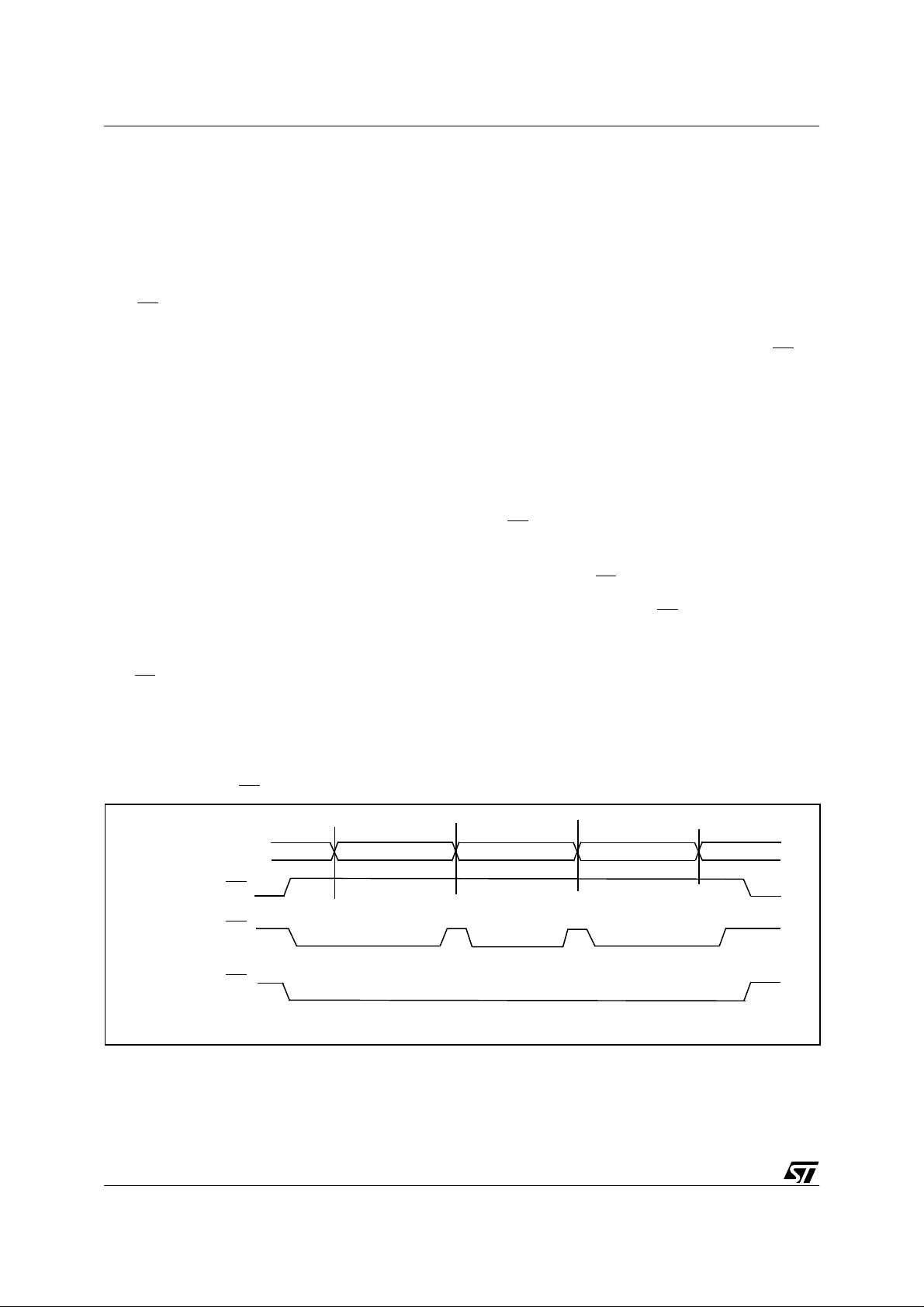
ST72E331 ST72T331
SERIAL PERIPHERAL INTERFACE (Cont’d)
5.6.4.3 Data Transfer Format
During an SPI transfer, data is simultaneously
transmitted (shifted out serially) and received
(shifted in serially). The serial clock is used to synchronize the data transfer during a sequence of
eight clock pulses.
The SS
device; the other slave devices that are not selected do not interfere with the SPI transfer.
Clock Phase and Clock Polarity
Four possible timing relationships may be chose n
by software, using the CPOL and CPHA bits.
The CPOL (clock polarity) bit cont rols the steady
state value of the clock when no data is being
transferred. This bit affects both m as ter and sl av e
modes.
The combination between the CPOL and CPHA
(clock phase) bits selects the data capture clock
edge.
Figure 4, shows an SPI transfer with the four com-
binations of the CPHA and CPOL bits. The diagram may be interpreted as a master or slave timing diagram where the SCK pin, the MISO pin, the
MOSI pin are directly connected between the master and the slave device.
The SS
be driven by the master device.
pin allows individual selection of a slave
pin is the slave device select input and can
The master device applies data to its MOSI pinclock edge before the capture clock edge.
CPHA bit is set
The second edge on the SCK pin (falling edg e if
the CPOL bit is reset, rising edge if the CPOL bit is
set) is the MSBit capture strobe. Data is latched on
the occurrence of the second clock transition.
No write collision should occur even if the SS
pin
stays low during a transfer of s everal bytes (see
Figure 3).
CPHA bit is reset
The first edge on the SCK pin (falling edge if CPOL
bit is set, rising ed ge if CPOL bit is reset ) is the
MSBit capture strobe. Data is latched on the oc currence of the first clock transition.
The SS
pin must be toggled high and low between
each byte transmitted (see Figure 3).
To protect the transmission from a write collision a
low value on the SS
pin of a slave device freezes
the data in its DR register and does not allow it to
be altered. Therefore the SS
pin must be high to
write a new data byte in the DR without producing
a write coll is ion .
Figure 42. CPHA / SS
MOSI/MISO
Master
SS
Slave SS
(CPHA=0)
Slave
SS
(CPHA=1)
74/107
74
Timing Dia gram
Byte 1 Byte 2
Byte 3
VR02131A
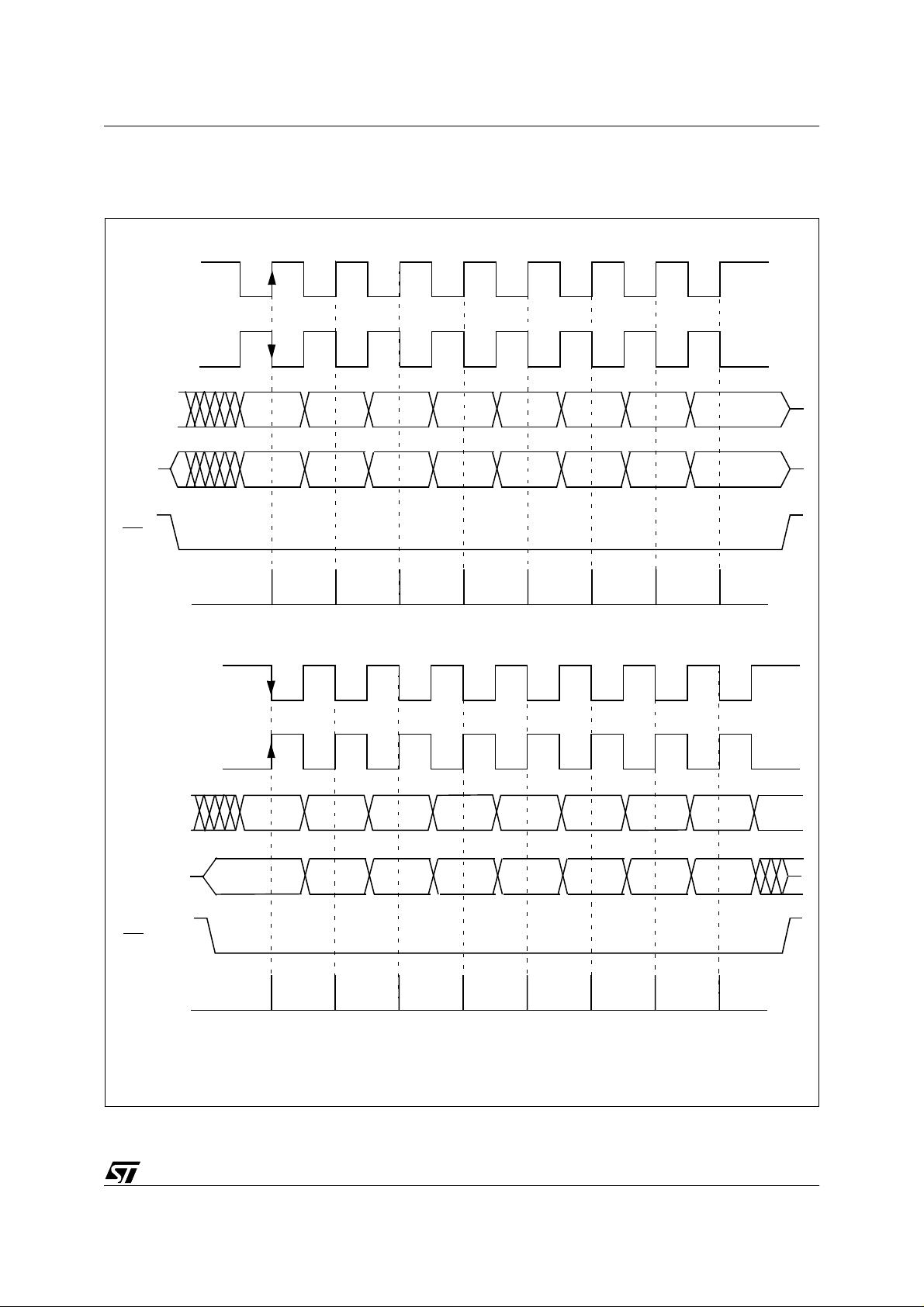
SERIAL PERIPHERAL INTERFACE (Cont’d)
Figure 43. D at a C lo ck Ti m in g D i agram
SCLK ( w ith
CPOL = 1)
SCLK ( w ith
CPOL = 0)
ST72E331 ST72T331
CPHA =1
MISO
(from master)
MOSI
(from slave)
SS
(to slave)
CAPTURE STROBE
CPOL = 1
CPOL = 0
MISO
(from master)
MSBit Bit 6 Bit 5
MSBit Bit 6 Bit 5
MSBit Bit 6 Bit 5
Bit 4 Bit3 Bit 2 Bit 1 LSBit
Bit 4 Bit3 Bit 2 Bit 1 LSBit
CPHA =0
Bit 4 Bit3 Bit 2 Bit 1 LSBit
MOSI
(from slave)
SS
(to slave)
CAPTURE STROBE
Note: This figure should not be used as a replacement for parametric information.
Refer to the Electrical Characteristics chapter.
MSBit Bit 6 Bit 5 Bit 4 Bit3 Bit 2 Bit 1 LSBit
VR02131B
75/107
75

ST72E331 ST72T331
SERIAL PERIPHERAL INTERFACE (Cont’d)
5.6.4.4 Write Collision Error
A write collision occurs when the software tries to
write to the DR register while a data transfer is taking place with an external dev ice. When t his happens, the transfer continues uninterrupted; and
the software w rit e w ill be uns u c c es s ful.
Write collisions can occur both in master and slave
mode.
Note: a "read collision" will never occur since the
received data byte is placed in a buffer in which
access is always synchronous with the MCU operation.
In Slave mode
When the CPHA bit is set:
The slav e device will re ceive a clock (S CK) ed ge
prior to the latch of the first data transfer. This first
clock edge will freeze t he d ata in the slave device
DR register and output the MSBit on to the external MISO pin of the slave device.
The SS
the output of the MSBit onto the MISO pin does
not take place until the first data transfer clock
edge.
pin low state enables the slave device but
When the CPHA bit is reset:
Data is latched on the occurrence of the first clock
transition. The slave device does not have any
way of knowing when that transition will occur;
therefore, the slave device collision occurs when
software attempts to write the DR register after its
pin has been pulled low.
SS
For this reason, the SS
pin must be high, between
each data byte transfer, to allow the CPU to write
in the DR register without generating a write collision.
In Master mode
Collision in the master device is defined as a write
of the DR register while the internal serial clock
(SCK) is in the process of transfer.
The SS
pin signal must be always high on the
master device.
WCOL bit
The WCOL bit in the SR register is set if a write
collision occurs.
No SPI interrupt is generated when the WCOL bit
is set (the WCOL bit is a status flag only).
Clearing the WCOL bit is done through a software
sequence (see Figure 5).
Figure 44. Clearing the WCOL bit (Write Collision Flag) Software Sequence
Clearing sequence after SPIF = 1 (end of a data byte transfer)
1st Step
2nd Step
Read SR
OR
THEN
Read DR Write D R
SPIF =0
WCOL=0
Read SR
THEN
SPIF =0
WCOL=0
WCOL=1 if a transfer has started
before the 2nd step
Clearing sequence before SPIF = 1 (during a data byte transfer)
1st Step
2nd Step
Read SR
Read DR
THEN
WCOL=0
Note: Writing in DR register instead of reading in it do not reset
WCOL bit
76/107
76
if no transfer has started

SERIAL PERIPHERAL INTERFACE (Cont’d)
5.6.4.5 Master Mode Fault
Master mode fault occurs when the master device
has its SS
pin pulled low, then the MODF bit is set.
Master mode fault affects the SPI peripheral in the
following ways:
– The MODF bit is set and an SPI interrupt is
generated if the SPIE bit is set.
– The SPE bit is reset. This blocks all output
from the device and disables the SPI peripheral.
– The MSTR bit is reset, thus forcing the device
into slave mode.
ST72E331 ST72T331
may be restored to their original state during or after this clearing sequence.
Hardware does not allow the user to set the SPE
and MSTR bits while the MODF bit is set except in
the MODF bit clearing sequence.
In a slave device the MODF bit can not be set, but
in a multi master configuration the device can be in
slave mode with this MODF bit set.
The MODF bit indicates that there might have
been a multi-master conflict for system control and
allows a proper exit from system operation to a reset or default system state using an interrupt routine.
Clearing the MODF bit is done through a software
sequence:
1. A read or write access to the SR register while
the MODF bit is set.
2. A write to the CR register.
Notes: To avoid any multiple slave conflicts in the
case of a system comprising several MCUs, the
SS
pin must be pulled high during the clearing se-
quence of the MODF bit. The SPE and MSTR bits
5.6.4.6 Overrun Condition
An overrun condition occurs w hen the mas ter device has sent several data bytes and the slave device has not cleared the S PIF bit issuing from the
previous data byte transmitted.
In this case, the rec eiver buffer contains the b yte
sent after the SPIF bit was last cleared. A read to
the DR register returns this byte. All other bytes
are lost.
This condition is not detected by the SPI peripheral.
77/107
77
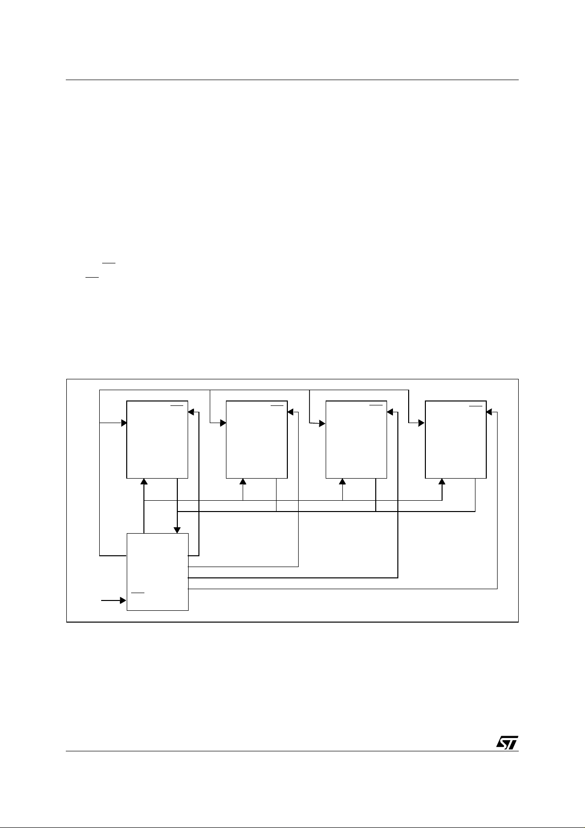
ST72E331 ST72T331
SERIAL PERIPHERAL INTERFACE (Cont’d)
5.6.4.7 Single Master and Multimaster Configura tions
There are two types of SPI systems:
– Single Master Syste m
– Multimaster System
Single Master System
A typical single master system may be configured,
using an MCU as the master and four MCUs as
slaves (see Figure 6).
The master device selects the individual slave devices by using four pins of a parallel port to control
the four SS
The SS
pins of the slave devices.
pins are pulled high during reset since the
master device ports will be forced to be inputs at
that time, thus disabling the slave devices.
Note: T o prevent a b us conflict on the MISO line
the master allows only one active slave device
during a transmission.
For more security, the slave device may respond
to the master with the received data byte. Then the
master will receive the previous byte back from the
slave device if all MISO and MOSI pins are connected and the slave has not written its DR register.
Other transmission security methods can use
ports for handshake lines or data by tes with command fields.
Multi-master System
A multi-master system may al so be configured by
the user. Transfer of master control could be implemented using a handshake method through the
I/O ports or by an exchange of code messages
through the serial peripheral interface system.
The multi-master system is principally handled by
the MSTR bit in the CR register and the MODF bit
in the SR register.
Fig u re 45. Singl e Master Co nfiguration
SS
SCK
SCK
Slave
MCU
MOSI
MOSI
MISO
MOSI MOSI MOSIMISO MISO MISOMISO
SCK
Master
5V
MCU
SS
Ports
Slave
MCU
SS
SS
SCK SCK
Slave
MCU
SS
Slave
MCU
78/107
78
ST72E331 ST72T331
SERIAL PERIPHERAL INTERFACE (Cont’d)
5.6.5 Low Power Modes
Mode Description
WAIT
HALT
5.6.6 Interrupts
No effect on SPI.
SPI interrupt events cause the device to exit from WAIT mode.
SPI registers are frozen.
In HALT mode, the SPI is inactive. SPI operation resumes when the MCU is woken up by an interrupt with
“exit from HALT mode” capability.
Interrupt Event
SPI End of Transfer Event SPIF
Master Mode Fault Event MODF Yes No
Event
Flag
Enable
Control
Bit
SPIE
Exit
from
Wait
Yes No
Note: The SPI interrupt even ts are connected to
the same interrupt vector (see Interrupts chapter).
They generate an interrupt if the corresponding
Enable Control Bit is set and the interrupt ma sk in
the CC register is reset (RIM instruction).
Exit
from
Halt
79/107
79

ST72E331 ST72T331
SERIAL PERIPHERAL INTERFACE (Cont’d)
5.6.7 Register Description
CONTROL REGISTER (CR)
Read/Write
Reset Value: 0000xxxx (0xh)
70
SPIE SPE SPR2 MSTR CPOL CPHA SPR1 SPR0
Bit 7 = SPIE
Serial peripheral interrupt enable.
This bit is set and cleared by software.
0: Interrupt is inhibited
1: An SPI interrupt is generated whenever SPIF=1
or MODF=1 in the SR register
Bit 6 = SPE
Serial peripheral output enable.
This bit is set and cleared by software. It is also
cleared by hardware when, in master mode, SS
=0
(see Section 0.1.4.5 Master Mode Fault).
0: I/O port connected to pins
1: SPI alternate functions connected to pins
The SPE bit is cleared by reset, so the SPI peripheral is not initially connected to the external pins.
Bit 3 = CPOL
Clock polarity.
This bit is set and cleared by software. This bit determines the steady state of the serial Clock. The
CPOL bit affects both the master and slave
modes.
0: The steady state is a low value at the SCK pin.
1: The steady state is a high value at the SCK pin.
Bit 2 = CPHA
Clock phase.
This bit is set and cleared by software.
0: The first clock transition is the first data capture
edge.
1: The second clock transition is the first capture
edge.
Bit 1:0 = SPR[1:0]
Serial peripheral rate.
These bits are set and c leared by software.Used
with the SPR2 bit, they select one of six baud rates
to be used as the serial clock when the device is a
master.
These 2 bits have no effect in slave mode.
Bit 5 = SPR2
Divider Enable
.
this bit is set and cleared by software and it is
cleared by reset. It is used with the SPR[1:0] bits to
set the baud rate. Refer to Table 1.
0: Divider by 2 enabled
1: Divider by 2 disabled
Bit 4 = MSTR
Master.
This bit is set and cleared by software. It is also
cleared by hardware when, in master mode, SS
=0
(see Section 0.1.4.5 Master Mode Fault).
0: Slave mode is selected
1: Master mode is selected, the function of the
SCK pin changes from an input to an output and
the functions of the MISO and MOSI pins are reversed.
Table 18. Serial P eri pheral Baud Rat e
Serial Clock SPR2 SPR1 SPR0
f
/4 1 0 0
CPU
/8 0 0 0
f
CPU
/16 0 0 1
f
CPU
/32 1 1 0
f
CPU
f
/64 0 1 0
CPU
/128 0 1 1
f
CPU
80/107
80

SERIAL PERIPHERAL INTERFACE (Cont’d)
STATUS REGISTER (SR)
Read Only
Reset Value: 0000 0000 (00h)
ST72E331 ST72T331
DATA I/O REGISTER (DR)
Read/Write
Reset Value: Undefined
70
SPIFWCOL-MODF----
Bit 7 = SPIF
Serial Peripheral data transfer flag.
This bit is set by hardware when a transfer has
been completed. An interrupt is generated if
SPIE=1 in the CR register. It is cleared by a software sequence (an access to the SR register followed by a read or write to the DR register).
0: Data transfer is in progress or has been ap-
proved by a clearing sequence.
1: Data transfer between the device and an exter-
nal device has been completed.
Note: While the SPIF bit is set, all writes to the DR
register are inhibited.
Bit 6 = WCOL
Write Collision status.
This bit is set by hardware when a write to the DR
70
D7 D6 D5 D4 D3 D2 D1 D0
The DR register is used to transmit and receive
data on the serial bus. In the master device only a
write to this register will initiate transmission/reception of another byte.
Notes: During the last clock cycle t he SPIF bit is
set, a copy of the received data byte in the shift
register is moved to a buffer. When the user reads
the serial peripheral data I/O register, the buffer is
actually being read.
Warning:
A write to the DR regis ter places da ta directly into
the shift reg ister for transmission.
A write to the the DR register returns the valu e located in the buffer and not the contents of the shift
register (See Figure 2 ).
register is done during a transmit sequence. It is
cleared by a software sequence (see Figure 5).
0: No write collision occurred
1: A write collision has been detected
Bit 5 = Unused.
Bit 4 = MODF
Mode Fau lt fl ag.
This bit is set by hardware when the SS pin is
pulled low in master mode (see Section 0.1.4.5
Master Mode Fault). An SPI interrupt can be gen-
erated if SPIE=1 in the CR register. This bit is
cleared by a software sequence (An access to the
SR register while MODF=1 followed by a write to
the CR register).
0: No master mode fault detected
1: A fault in master mode has been detected
Bits 3-0 = Unused.
81/107
81

ST72E331 ST72T331
Table 19. SPI Register Map and Reset Values
Address
(Hex.)
21
22
23
Register
Name
DR
Reset Value
CR
Reset Value
SR
Reset Value
76543210
D7
x
SPIE
0
SPIF
0
D6
x
SPE
0
WCOL
0
D5
x
SPR20MSTR0CPOL
-
0
D4
x
MODF
0
D3
x
x
-
0
D2
x
CPHAxSPR1
-
0
D1
x
x
-
0
D0
x
SPR0
x
-
0
82/107
82

5.7 8-BIT A/D CONVERTER (ADC)
ST72E331 ST72T331
5.7.1 Introd uction
The on-chip Analog to Digital Converter ( ADC) peripheral is a 8-bit, successive approximation converter with internal sample and hold circuitry. This
peripheral has up to 8 multiplexed analog input
channels (refer to device pin out description) that
allow the peripheral to convert the analog vol tage
levels from up to 8 different sources.
The result of the conversion is stored in a 8-bit
Data Register. The A/D converter is controlled
through a Control/Status Register.
Figure 46. ADC Block Diagram
AIN0
AIN1
AIN2
AIN3
AIN4
AIN5
AIN6
AIN7
ANALOG
MUX
SAMPLE
&
HOLD
5.7.2 Main Features
■ 8-bit conversion
■ Up to 8 channels with multiplexed input
■ Linear successive approximation
■ Data register (DR) which contains the results
■ Conversion complete status flag
■ On/Off bit (to reduce consumption)
The block diagram is shown in Figure 1.
COCO
0CH0CH1CH2--ADON
(Control Status Register) CSR
ANALOG TO
DIGITAL
CONVERTER
f
CPU
AD7
AD4 AD0AD1AD2AD3AD6 AD5
(Data Register) DR
83/107
83

ST72E331 ST72T331
8-BIT A/D CONVERTER (ADC) (Cont’d)
5.7.3 Functional Description
The high level reference voltage V
connected externally to the V
reference voltage V
nally to the V
pin. In some devices (refer to de-
SS
must be connected exter-
SSA
pin. The low level
DD
vice pin out description) high and low level reference voltages are internally c onnected to the V
and VSS pins.
Conversion accuracy may therefore be degraded
by voltage drops and noise in the event of hea vily
loaded or badly decoupled power supply lines.
Figure 47. Recommended Ext. Connections
V
DD
V
AIN
R
AIN
0.1µF
Characteristics:
The conversion is monotonic, meaning the result
never decreases if the analog input does not an d
never increases if the analog input does not.
If input voltage is greater than or equal to V
(voltage reference high) then results = FFh (full
scale) without overflow indication.
If input voltage ≤ V
(vol tage refe rence low) t hen
SS
the results = 00h.
The conversion time is 64 CPU clock cycles in-
cluding a sampling time of 31.5 CPU clock cycles.
is the maximum recommended impedance
R
AIN
for an analog input signal. If the impedance is too
high, this will result in a loss of accuracy due to
leakage and sampling not being completed in the
alloted time.
The A/D converter is linear and the digital result of
the conversion is given by the formula:
Digital res ult =
255 x Input Voltage
Reference Voltage
must be
DDA
V
DDA
V
SSA
ST7
Px.x/AINx
DD
DD
The accuracy of the conversion is described in the
Electrical Characteristics Section.
Procedure:
Refer to the CSR and DR register description section for the bit definitions.
Each analog input pin must be configured as input,
no pull-up, no interrupt. Refer to the “I/O Ports”
chapter. Using these p ins as analog inputs does
not affect the ability of the port to be r ead as a logic
input.
In the CSR register:
– Select the CH2 to CH0 bits to assign the ana-
log channel to convert. Refer to Table 1.
– Set the ADON bit. Then the A /D converter is
enabled after a stabilization time (typically 30
µs). It then performs a c ontinuou s conv ersion
of the selected channel.
When a conversion is complete
– The COCO bit is set by hardware.
– No interrupt is generated.
– The result is in the DR register.
A write to the CSR register aborts the current conversion, resets the COCO bit and starts a new
conversion.
5.7.4 Low Power Modes
Note: The A/D converter may be disabled by re-
setting the ADON bit. This feature allows reduced
power consumption when no conversion is needed.
Mode Description
WAIT No effect on A/D Converter
A/D Converter disabled.
After wakeup from Halt mode, the A/D
HALT
Converter requires a stabilisation time
before accurate conversions can be
performed.
5.7.5 Interrupts
None.
Where Reference Voltage is V
84/107
84
DD
- VSS.
ST72E331 ST72T331
8-BIT A/D CONVERTER (ADC) (Cont’d)
5.7.6 Register Description
CONTROL/STATUS REGISTER (CSR)
Read/Write
Reset Value: 0000 0000 (00h)
70
COCO - ADON 0 - CH2 CH1 CH0
Bit 7 = COCO
Conversion Complete
This bit is set by hardware. It is cleared by software reading the result in the DR register or writing
to the CSR register.
0: Conversion is not complete.
1: Conversion can be read from the DR register.
These bits are set and cleared by so ftware. They
select the analog input to convert.
Table 20. Channel Selection
Pin* CH2 CH1 C H0
AIN0 000
AIN1 001
AIN2 010
AIN3 011
AIN4 100
AIN5 101
AIN6 110
AIN7 111
Bit 6 = R eserved . Must always be cleared.
Bit 5 = ADON
A/D converter On
This bit is set and cleared by software.
0: A/D converter is switched off.
1: A/D converter is switched on.
Note: A typical 30 µs delay time is necessary for
the ADC to stabilize when the ADO N b it is set.
Bit 4 = R eserved . Forced by hardware to 0.
Bit 3 = R eserved . Must always be cleared.
Bits 2:0: CH[2:0]
Channel Selection
Table 21. ADC Register Map
Address
(Hex.)
70
Reset Value
71
Reset Value
Register
Name
DR
CSR
76543210
AD7
0
COCO
0
AD6
0
-
0
ADON
*IMPORTANT NOTE:
The number of pins AND
the channel selection vary according to the device.
REFER TO THE DEVICE PINOUT).
DATA REGISTER (DR)
Read Only
Reset Value: 0000 0000 (00h)
70
AD7AD6AD5AD4AD3AD2AD1AD0
Bit 7:0 = AD[7:0]
Analog Converted Value
This register contains the converted analog value
in the range 00h to FFh.
Reading this register resets the COCO flag.
AD5
0
0
AD4
0
0
0
AD3
0
-
0
AD2
0
CH2
0
AD1
0
CH1
0
AD0
0
CH0
0
85/107
85

ST72E331 ST72T331
6 INSTRUCTION SET
6.1 ST7 ADDRESSING MODES
The ST7 Core features 17 different addressing
modes which can be classified in 7 main groups:
Addressing Mode Example
Inherent nop
Immediate ld A,#$55
Direct ld A,$55
Indexed ld A,($55,X)
Indirect ld A,([$55],X)
Relative jrne loop
Bit operation bset byte,#5
so, most of the ad dressing modes may be subdivided in two sub-modes called long and short:
– Long addressing mode is more powerful be-
cause it can use the full 64 Kbyte address space,
however it uses more bytes and more CPU cycles.
– Short addressing mode is less powerful because
it can generally only access page zero (0000h 00FFh range), but the instruction size is more
compact, and faster. All memory to memory instructions use short addressing modes only
(CLR, CPL, NEG, BSET, BRES, BTJT, BTJF,
INC, DEC, RLC, RRC, SLL, SRL, SRA, SWAP)
The ST7 Assembler optimizes the use of long and
short addressing modes.
The ST7 Instruction set is designed to minimize
the number of bytes required per instruction: To do
Table 22. ST7 Addressing Mode Overview
Mode Syntax
Inherent nop + 0
Immediate ld A,#$55 + 1
Short Direct ld A,$10 00..FF + 1
Long Direct ld A,$1000 0000..FFFF + 2
No Offset Direct Indexed ld A,(X) 00..FF
Short Direct Indexed ld A,($10,X) 00..1FE + 1
Long Direct Indexed ld A,($1000,X) 0000..FFFF + 2
Short Indirect ld A,[$10] 00..FF 00..FF byte + 2
Long Indirect ld A,[$10.w] 0000..FFFF 00..FF word + 2
Short Indirect Indexed ld A,([$10],X) 00..1FE 00..FF byte + 2
Long Indirect Indexed ld A,([$10.w],X) 0000..FFFF 00..FF word + 2
Relative Direct jrne loop PC-128/PC+1 27
Relative Indirect jrne [$10] PC -128 /PC+1 27
Bit Direct bset $10,#7 00..FF + 1
Bit Indirect bset [$10],#7 00..FF 00..FF byte + 2
Bit Direct Relative btjt $10,#7,skip 00..FF + 2
Bit Indirect Relative btjt [$10],#7,skip 00..FF 00..FF byte + 3
Destination/
Source
Pointer
Address
(Hex.)
1)
1)
00..FF byte + 2
Pointer
Size
(Hex.)
Length
(Bytes)
+ 0 (with X register)
+ 1 (with Y register)
+ 1
Note 1. At the time the instruction is executed, the Program Counter (PC) points to the instruction following JRxx.
86/107
86
ST7 ADDRESSING MODES (Cont’d)
6.1.1 Inherent
All Inherent instructions consist of a single byte.
The opcode fully specifies all the required information for the CPU to process the operation.
Inherent Instruction Function
NOP No operation
TRAP S/W Interrupt
WFI
HALT
RET Sub-routine Return
IRET Interrupt Sub-routine Return
SIM Set Interrupt Mask
RIM Reset Interrupt Mask
SCF Set Carry Flag
RCF Reset Carry Flag
RSP Reset Stack Pointer
LD Load
CLR Clear
PUSH/POP Push/Pop to/from the stack
INC/DEC Increment/Decrement
TNZ Test Negative or Zero
CPL, NEG 1 or 2 Complement
MUL Byte Multiplication
SLL, SRL, SRA, RLC,
RRC
SWAP Swap Nibbles
Wait For Interrupt (Low Power
Mode)
Halt Oscillator (Lowest Power
Mode)
Shift and Rotate Operations
6.1.2 Immediate
Immediate instructions have two bytes, the first
byte contains the opcode, the second byte contains the operand value.
Immediate Instruction Function
LD Load
CP Compare
BCP Bit Compare
AND, OR, XOR Logical Operations
ADC, ADD, SUB, SBC Arithmetic Operations
ST72E331 ST72T331
6.1.3 Direct
In Direct instructions, the operands are referenced
by their memory address.
The direct addressing m ode consists of two submodes:
Direct (short)
The address is a byte, thus requires only one byte
after the opcode, but only allows 00 - FF addressing space.
Direct (lon g)
The address is a word, thus allowing 64 Kbyte addressing space, but requires 2 bytes after the opcode.
6.1.4 Indexed (No Offset, Short, Long)
In this mode, the operand is referenced by its
memory address, which is defined by the unsigned
addition of an index register (X or Y) with an offset.
The indirect addressing mode consists of three
sub-modes:
Indexed (No Offset)
There is no offset, (no extra byte after the opcode),
and allows 00 - FF addressing space.
Indexed (Short)
The offset is a byte, thus requires only one byte after the opcode and allows 00 - 1FE addressing
space.
Indexed (long)
The offset is a word, thus allowing 64 Kbyte addressing space and requires 2 byt es after the opcode.
6.1.5 Indirect (Short, Long)
The required data byte to do the operation is found
by its memory address, located in memory (pointer).
The pointer address follows th e op co de. Th e i ndirect addressing mode consists of two sub-modes:
Indirect (short)
The pointer address is a byte, the pointer size is a
byte, thus allowing 00 - FF addressing space, and
requires 1 byte after the opcode.
Indirect (lon g)
The pointer address is a byte, the pointer size is a
word, thus allowing 64 Kbyte addressing space,
and requires 1 byte after the opcode.
87/107
87

ST72E331 ST72T331
ST7 ADDRESSING MODES (Cont’d)
6.1.6 Indi re ct In dexed (Shor t, Long)
This is a combination of indirect and short indexed
addressing modes. The operand is referenced by
its memory address, which is defined by the unsigned addition of an index register value (X or Y)
with a pointer value located in memory. The pointer address follows the opcode.
The indirect indexed addressing mode consists of
two sub-modes:
Indirect Indexed (Short)
The pointer address is a byte, the pointer size is a
byte, thus allowing 00 - 1FE addressing space,
and requires 1 byte after the opcode.
Indirect Inde xed (Long)
The pointer address is a byte, the pointer size is a
word, thus allowing 64 Kbyte addressing space,
and requires 1 byte after the opcode.
Table 23. Instructions Supporting Direct,
Indexed, Indirect and Indirect Indexed
Addressing Modes
SWAP Swap Nibbles
CALL, JP Call or Jump subroutine
6.1.7 Relative Mode (Direct, Indirect)
This addressing mode is used to m odify the PC
register value by adding an 8-bit signed offset to it.
Available Relative Direct/
Indirect Instructions
JRxx Conditional Jump
CALLR Call Relative
Function
The relative addressing mode consists of two submodes:
Relative (Direct)
The offset follows the opcode.
Relative (Indirect)
The offset is defined in memory, of which t he address follows the opcode.
Long and Short
Instructions
LD Load
CP Compare
AND, OR, XOR Logical Operations
ADC, ADD, SUB, SBC
BCP Bit Compare
Short Instructions Only Function
CLR Clear
INC, DEC Increment/Decrement
TNZ Test Negative or Zero
CPL, NEG 1 or 2 Complement
BSET, BRES Bit Operations
BTJT, BTJF
SLL, SRL, SRA, RLC,
RRC
Arithmetic Addition/subtraction operations
Bit Test and Jump Operations
Shift and Rotate Operations
Function
88/107
88

6.2 INSTRUCTION GROUPS
ST72E331 ST72T331
The ST7 family devices use an Instruction Set
consisting of 63 instructions. The instructions may
Load and Transfer LD CLR
Stack operation PUSH POP RSP
Increment/Decrement INC DEC
Compare and Tests CP TNZ BCP
Logical operations AND OR XO R CPL NEG
Bit Operation BSET BRES
Conditional Bit Test and Branch BTJT BTJF
Arithmetic operations ADC ADD SUB SBC MUL
Shift and Rotates SLL SRL SRA RLC RRC SWAP SLA
Unconditional Jump or Call JRA JRT JRF JP CALL CALLR NOP RET
Conditional Branch JRxx
Interruption management TRAP WFI HALT IRET
Code Condition Flag modification SIM RIM SCF RCF
be subdivided into 13 main groups as illustrated in
the following table:
Using a pre-b y te
The instructions are described with one to four
bytes.
In order to extend the number of available opcodes for an 8-bit CPU (256 opcodes), three different prebyte opcodes a re defined . These prebytes
modify the meaning of the instruction they precede.
The whole instruction becomes:
PC-2 End of previous instruction
PC-1 Prebyte
PC Opcode
PC+1 Addi tional word (0 to 2) according to the
number of bytes required to compute the
effective address
These prebytes enable instruction in Y as well as
indirect addressing modes to be implemented.
They precede the opcode of the instruction in X or
the instruction using direct addres sing mode . The
prebytes are:
PDY 90 Replace an X based instruction using
immediate, direct, indexed, or inherent
addressing mode by a Y one.
PIX 92 Replace an instruction using direct, di-
rect bit, or direct relative addressing
mode to an instruction using the corresponding indirect addressing mode.
It also changes an instruction using X
indexed addressing mode to an instruction using indirect X indexed addressing
mode.
PIY 91 Repla ce an instruction using X indirect
indexed addressing mode by a Y one.
89/107
89
ST72E331 ST72T331
INSTRUCTION GROUPS (Cont’d)
Mnemo Description Function/Example Dst Src H I N Z C
ADC Add with Carry A = A + M + C A M H N Z C
ADD Addition A = A + M A M H N Z C
AND Logical And A = A . M A M N Z
BCP Bit compare A, Memory tst (A . M) A M N Z
BRES Bit Reset bres Byte, #3 M
BSET Bit Set bset Byte, #3 M
BTJF Jump if bit is false (0) btjf Byte, #3, Jmp1 M C
BTJT Jump if bit is true (1) btjt Byte, #3, Jmp1 M C
CALL Call subroutine
CALLR Call subro utine relative
CLR Clear reg, M 0 1
CP Arithmetic Compare tst(Reg - M) reg M N Z C
CPL One Complement A = FFH-A reg, M N Z 1
DEC Decrement dec Y reg, M N Z
HALT Halt 0
IRET Interrupt routine return Pop CC, A, X, PC H I N Z C
INC Increment inc X reg, M N Z
JP Abs olute Jump jp [TBL.w]
JRA Jump relative always
JRT Jump relative
JRF Never jump jrf *
JRIH Jump if ext. interrupt = 1
JRIL Jump if ext. interrupt = 0
JRH Jump if H = 1 H = 1 ?
JRNH Jump if H = 0 H = 0 ?
JRM Jump if I = 1 I = 1 ?
JRNM Jump if I = 0 I = 0 ?
JRMI Jump if N = 1 (minus) N = 1 ?
JRPL Jump if N = 0 (plus) N = 0 ?
JREQ Jump if Z = 1 (equal) Z = 1 ?
JRNE Jump if Z = 0 (not equal) Z = 0 ?
JRC Jump if C = 1 C = 1 ?
JRNC Jump if C = 0 C = 0 ?
JRULT Jump if C = 1 Unsigned <
JRUGE Jump if C = 0 Jmp if unsigned >=
JRUGT Jump if (C + Z = 0) Unsigned >
90/107
90

ST72E331 ST72T331
INSTRUCTION GROUPS (Cont’d)
Mnemo Description Function/Example Dst Src H I N Z C
JRULE Jump if (C + Z = 1) Unsigned <=
LD Load dst <= src reg, M M, reg N Z
MUL Multiply X,A = X * A A, X, Y X, Y, A 0 0
NEG Negate (2’s compl) neg $10 reg, M N Z C
NOP No Operation
OR OR operation A = A + M A M N Z
POP Pop from the Stack pop reg reg M
pop CC CC M H I N Z C
PUSH Push onto the Stack push Y M reg, CC
RCF Reset carry flag C = 0 0
RET Subroutine Return
RIM Enable Interrupts I = 0 0
RLC Rotate left true C C <= Dst <= C reg, M N Z C
RRC Rotate right true C C => Dst => C reg, M N Z C
RSP Reset Stack Pointer S = Max allowed
SBC Subtract with Carry A = A - M - C A M N Z C
SCF Set carry flag C = 1 1
SIM Disable Interrupts I = 1 1
SLA Shift left Arithmetic C <= Dst <= 0 reg, M N Z C
SLL Shift left Logic C <= Dst <= 0 reg, M N Z C
SRL Shift right Logic 0 => Dst => C reg, M 0 Z C
SRA Shift right Arithmetic Dst7 => Dst => C reg, M N Z C
SUB Subtraction A = A - M A M N Z C
SWAP SWAP nibbles Dst[7..4] <=> Dst[3..0] reg, M N Z
TNZ Test for Neg & Zero tnz lbl1 N Z
TRAP S/W trap S/W interrupt 1
WFI Wait for Interrupt 0
XOR Exclusive OR A = A XOR M A M N Z
91/107
91

ST72E331 ST72T331
7 ELECTRIC AL CHARACTERI S TI CS
7.1 ABSOLUTE MAXIMUM RATINGS
This product contains devices to protect the inputs
against damage due to high static voltages , however it is advisable to take normal precaution to
avoid application of any voltage higher than the
specified maximum rated voltages.
For proper operation it is recommended that V
and VO be higher t han VSS and lower than VDD.
Reliability is enhanc ed if unused inputs are connected to an appropriate logic vol tage level (V
or VSS).
DD
Power Considerations.The average chip-junction temperature, T
from:
Where: T
I
T
=TA + PD x RthJA
J
= Ambient Temperature.
A
RthJA = Package thermal resistanc e
, in Celsius can be obtained
J
(junction-to ambient).
= P
P
D
P
=IDD x VDD (chip internal power).
INT
P
PORT
INT
+ P
PORT
.
=Port power dissipation
determined by the user)
Symbol Parameter Value Unit
Digital Supply Voltage -0.3 to 6.0 V
Analog Supply and Reference Voltage VDD - 0.3 to VDD + 0.3 V
Input Voltage VSS - 0.3 to VDD + 0.3 V
- 0.3 to VDD + 0.3
V
Analog Input Voltage (A/D Converter)
Output Voltage VSS - 0.3 to VDD + 0.3 V
Total Current into VDD (source) 100 mA
Total Current out of VSS (sink) 100 mA
Junction Temperature 150 °C
Storage Temperature -60 to 150 °C
V
SS
SSA
-0.3 to V
DDA
+0.3
V
IV
IV
T
V
V
DD
DDA
V
AI
V
O
DD
SS
T
STG
I
J
V
Note: Stresses above those listed as “absolute maximum ratings” may cause permanent damage to the device. This is
a stress rating only and functional operation of the device at these conditions is not implied. Exposure to maximum
rating conditions for extended periods may affect device reliability.
92/107
92
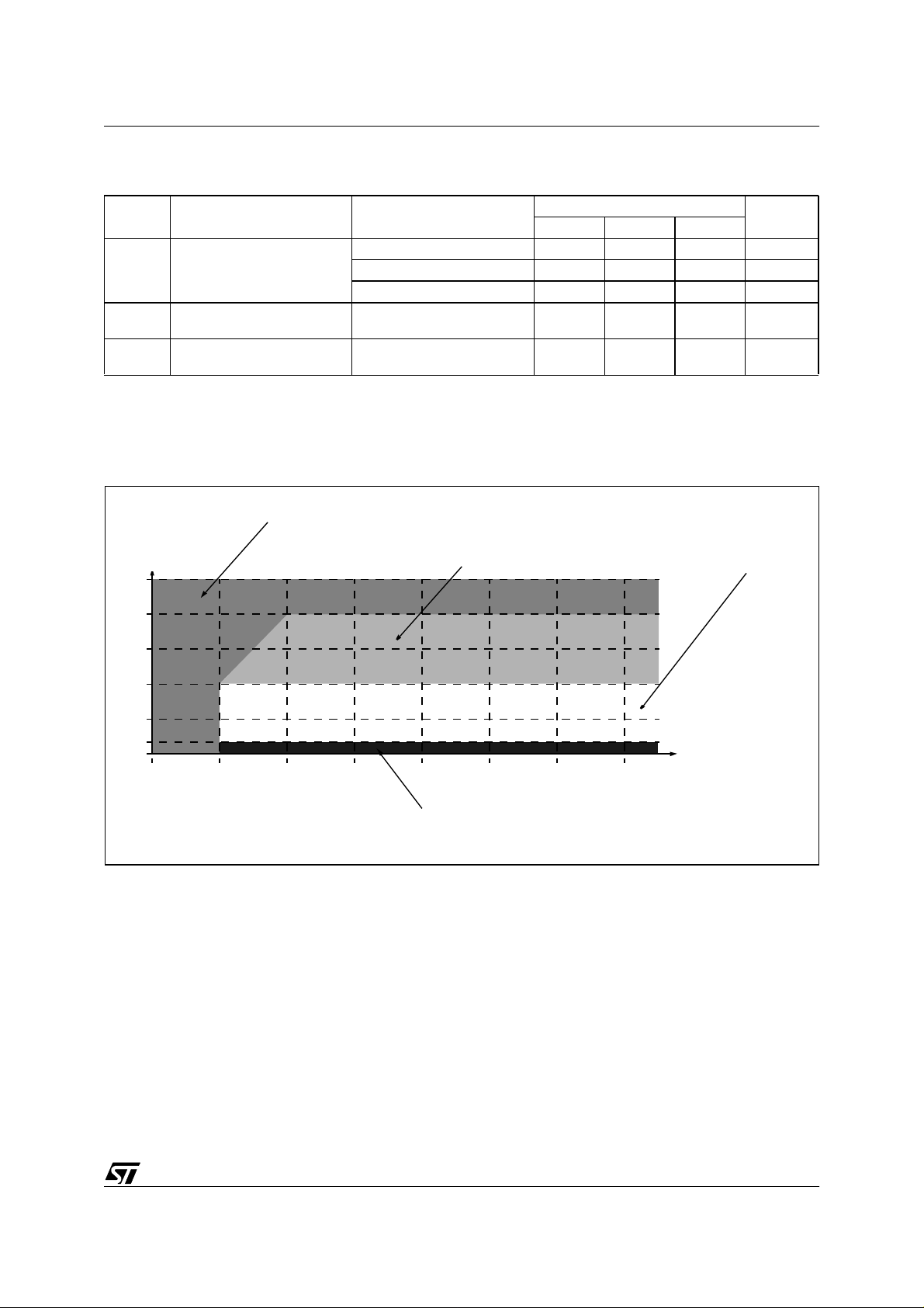
7.2 RECOMMENDED OPERATING CONDITIONS
ST72E331 ST72T331
Symbol Parameter Test Conditions
Min. Typ. Max.
1 Suffix Version 0 70 °C
T
Operating Temperature
A
6 Suffix Version -40 85 °C
3 Suffix Version -40 125 °C
V
f
OSC
Operating Supply Voltage
DD
Oscillator Frequency
16 MHz (1 & 6 Suffix)
OSC =
f
8 MHz
OSC =
V
= 3.0V
DD
V
= 3.5V (1 & 6 Suffix)
DD
3.5
3.0
0
0
2)
2)
f
Note
1) A safe reset (with Low Voltage Detector option) is not guaranteed at 16 MHz.
2) A/D operation and Oscillator start-up are not guaranteed below 1MHz.
Figure 48. Maximum Operating Frequency (f
FUNCTIONALITY NOT GUARANTEED IN THIS AREA
FUNCTIONALITY NOT GUARANTEED IN THIS AREA
FOR TEMPERATURE HIGHER THAN 85°C
16
f
OSC
[MHz]
) Versus Supply Voltage (VDD)
OSC
Value
1)
5.5
5.5
8
16
FUNCTIONALITY GUARANTEED IN THIS AREA
Unit
V
MHz
8
4
1
0
2.5 3 3.5 4 4.5 5 5.5 6
FUNCTIONALITY NOT GUARANTEED IN THIS AREA WITH RESONATOR
Supplly Voltage
[V]
93/107
93
ST72E331 ST72T331
7.3 RESET CHARACTERISTICS
(T
=-40...+125oC and VDD=5V±10% unless otherwise specified.
A
Symbol Parameter Conditions Min Typ
VIN > V
R
t
RESET
t
PULSE
Reset Weak Pull-up R
ON
Pulse duration generated by watchdog and POR reset
Minimum pulse duration to be applied on external RESET
ON
pin
VIN < V
IH
IL
Note:
1) These values given only as design guidelines and are not tested.
7.4 OSCILLATOR CHARACTERISTICS
(T
= -40°C to +125°C unless otherwise specified)
A
Symbol Paramete r Test Conditions
g
f
OSC
t
start
Oscillator transconductance 2 9 mA/V
m
Crystal frequ ency 1 16 MHz
Osc. start up time VDD = 5V±10% 50 ms
Min. Typ. Max.
10
20
60
1)
Value
40
120
1
1)
Max Unit
80
240
k
Ω
s
µ
ns
Unit
94/107
94
ST72E331 ST72T331
7.5 DC ELECTRICAL CHARACTERISTICS
(T
= -40°C to +125°C and VDD = 5V unless otherwise specified)
A
Symbol Parameter Test Conditions
V
Input Low Level Voltage
V
IL
All Input pins
Input High Level Voltage
V
IH
All Input pins
Hysteresis Voltage
HYS
All Input pins
Low Level Output Voltage
All Output pins
V
OL
Low Level Output Voltage
High Sink I/O pins
High Level Output Voltage
V
OH
All Output pins
Input Leakage Current
I
IL
All Input pins but RESET
I
IH
Input Leakage Current
I
IH
RESET pin
Reset Weak Pull-up R
R
ON
R
I/O Weak Pull-up R
PU
Supply Current in
RUN Mode
Supply Current in SLOW
2)
Mode
Supply Current in WAIT
I
DD
Mode
3)
Supply Current in WAITMINIMUM Mode
Supply Current in HALT
Mode
1)
PU
2)
5)
3V < V
3V < V
I
OL
I
OL
I
OL
I
OL
I
OL
I
OL
I
OH
I
OH
VIN = VSS (No Pull-up configured)
4)
V
IN
V
IN
VIN > V
ON
VIN < V
VIN < V
f
OSC
f
OSC
f
OSC
f
OSC
f
OSC
f
OSC
f
OSC
f
OSC
f
OSC
f
OSC
f
OSC
f
OSC
I
LOAD
I
LOAD
I
LOAD
< 5.5V VDD x 0.3 V
DD
< 5.5V VDD x 0.7 V
DD
= +10µA
= + 2mA
= +10µA
= +10mA
= + 15mA
= + 20mA, TA = 85°C max
= - 10µA
= - 2mA
= V
DD
= V
DD
IH
IL
IL
= 4 MHz, f
= 8 MHz, f
= 16 MHz, f
= 4 MHz, f
= 8 MHz, f
= 16 MHz, f
= 4MHz, f
= 8MHz, f
= 16MHz, f
= 4 MHz, f
= 8 MHz, f
= 16 MHz, f
CPU
CPU
CPU
CPU
CPU
CPU
CPU
CPU
CPU
CPU
CPU
CPU
= 2 MHz
= 4 MHz
= 125 kHz
= 250 kHz
= 2MHz
= 4 MHz
= 125 kHz
= 250 kHz
= 0mA without LVD, TA = 85°C max
= 0mA without LVD
= 0mA with LVD
= 8 MHz
= 500 kHz
= 8 MHz
= 500 kHz
Min. Typ. Max.
4.9
4.2
20
60
Notes:
1. Hysteresis voltage between switching levels. Based on characterisation results, not tested.
2. CPU running with memory access, no DC load or activity on I/O’s; clock input (OSCIN) driven by external square wave.
3. No DC load or activity on I/O’s; clock input (OSCIN) driven by external square wave.
4. Except OSCIN and OSCOUT
5. WAIT Mode with SLOW Mode selected. Based on characterisation results, not tested.
Value
400 mV
0.1
0.4
0.1
1.5
3.0
3.0
0.1 1.0
0.1 1.0
40
120
80
240
100 k
3.5
6
11
1.5
2.5
4.5
2
4
6.5
0.8
1
1.6
1
5
70
7
12
20
3
5
9
4
8
12
1.5
2
3.5
10
20
100
Unit
V
V
µ
k
Ω
Ω
mA
mA
mA
mA
µ
A
A
95/107
95

ST72E331 ST72T331
7.6 PERIPHERAL CHARACTERISTICS
Low Voltage Detection Reset Electrical Specifications (Option)
Symbol Parameter Conditions Min. Typ. Max. Unit
2)
V
LVDUP
V
LVDDOWN
V
LVDHYS
LVD Reset Trigger, VDD rising edge
LVD Reset Trigger, VDD falling edge 3.35 3.6 3.85 V
LVD Reset Trigger, hysteresis
2)
= 8 MHz max1).
f
OSC
Notes:
1. The safe reset cannot be guaranted by the LVD when fosc is greater than 8MHz.
2. Based on characterisation results, not tested.
EEPROM Specifications
Parameter Conditions Min Max Unit
25°C; 3.5V to 5.5V @ f
≤
T
A
85°C; 3.5V to 5.5V @ f
Write Time
≤
A
125°C; 3V to 5.5V @ f
≤
T
A
Write Erase Cycles T
Data Retention T
= 16 MHz, 3V to 5.5V @ f
OSC
= 16 MHz, 3V to 5.5V @ f
OSC
= 8 MHz 20
OSC
25°C 300,000 Cycles
=
A
55°C 10 Years
=
A
Note 1: Based on characterisation results, not tested
3.6
3.85 4.1 V
250 mV
= 8 MHz 10
OSC
= 8 MHz 15
OSC
1)
ms T
96/107
96
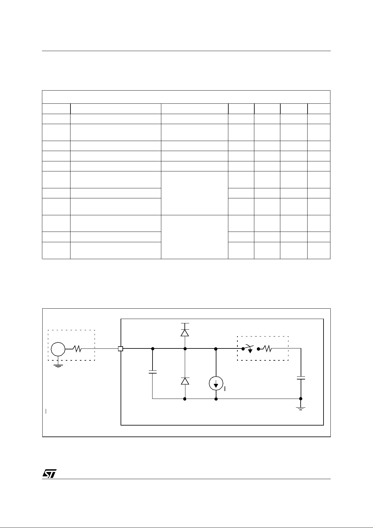
ST72E331 ST72T331
PERIPHERAL CHARACTERISTICS (Cont’d)
= -40°C to +125°C and VDD = 5V±10% unless otherwise specified )
(T
A
A/D Converter Specifications
Symbol Parameter Conditions Min Typ Max Unit
T
SAMPLE
Res ADC Resolution
DLE Differential Linearity Error* ±0.6 ±1
ILE Integral Linearity Error* ±2
V
AIN
I
ADC
t
STAB
t
CONV
R
AIN
C
HOLD
R
SS
Sample Duration 31.5 1/f
=8MHz
f
CPU
V
DD=VDDA
Analog Input Voltage V
=5V
SSA
Supply current rise
during A/D conversion
f
=8MHz
Stabilization time after ADC enable 30 µs
CPU
V
DD=VDDA
=5V
Conversion Time
Resistance of analog sources
(V
AIN)
Hold Capacitance 22 pF
f
=8MHz, T=25°C,
CPU
V
DD=VDDA
=5V
Resistance of sampling switch and
internal trace
8 bit
V
DDA
V
1mA
8
64
µs
1/f
15 K
2K
CPU
CPU
Ω
Ω
*Note:
For I
a loss of 1 LSB by 10K
ADC Accuracy vs. Negative Injection Current
=0.8mA, the typical leakage induced inside the die is 1.6µA and the effect on the ADC accuracy is
inj-
Ω increase of the external analog source impedance.
:
These measurements results and recommendat ions take worst case injection condi tions into account :
- negative injection
- injection to an Input with analog capability, adjacent to the enabled Analog Input
- at 5V V
V
C
pin
V
T
SS
C
hold
leakage
supply, and worst case temperature.
DD
R
AIN
AIN
Px.x/AINx
C
= input capacitance
5pF
= threshold voltage
= sampling switch
= sample/hold
capacitance
= leakage current
at the pin due
to various junctions
pin
V
DD
VT = 0.6V
= 0.6V
V
T
Sampling
SS
leakage max.
±1µA
Switch
2K
Ω
R
SS
C
hold
22 pF
V
SS
97/107
97

ST72E331 ST72T331
PERIPHERAL CHARACTERISTICS (Cont’d)
Figure 49. ADC Conversion characteristics
255
254
253
252
251
250
code
out
7
6
5
4
3
2
1
0
Offset Error OSE
Offset Error OSE
(2)
1LSB
1)
(
(5)
(4)
(3)
1 LSB (ideal)
1 2 3 4 5 6 7 250 251 252 253 254 255 256
(1) Example of an actual transfer curve
(2) The ideal transfer curve
(3) Differential non-linearity error (DLE)
(4) Integral non-linearity error (ILE)
(5) Center of a step of the actual transfer curve
V
in(A)
(LSB
ideal
)
Gain Error GE
V
refPVrefM
ideal
--------------------------------------- -=
–
256
VR02133A
98/107
PERIPHERAL CHARACTERISTICS (Cont’d)
Serial Peripheral Interface
ST72E331 ST72T331
Ref. Symbol Parameter Condition
f
SPI
1t
2t
3t
4t
5t
6t
7t
8t
9t
10 t
11 t
12 t
13 t
SPI
Lead
Lag
SPI_H
SPI_L
SU
H
A
Dis
V
Hold
Rise
Fall
SPI frequency
SPI clock period
Enable lead time Slave 120 ns
Enable lag time Slave 120 ns
Clock (SCK) high time
Clock (SCK) low time
Data set-up time
Data hold time (inputs)
Access time (time to data active
from high impedance state)
Disable time (hold time to high im-
pedance state)
Data valid
Data hold time (outputs)
Rise time
(20% V
to 70% VDD, CL = 200pF)
DD
Fall time
(70% V
to 20% VDD, CL = 200pF)
DD
Master
Slave
Master
Slave
Master
Slave
Master
Slave
Master
Slave
Master
Slave
Slave
Master (before capture edge)
Slave (after enable edge)
Master (before capture edge)
Slave (after enable edge)
Outputs: SCK,MOSI,MISO
Inputs: SCK,MOSI,MISO,SS
Outputs: SCK,MOSI,MISO
Inputs: SCK,MOSI,MISO,SS
Value
Min. Max.
1/128
dc
1/4
1/2
4
2
100
90
100
90
100
100
100
100
0 120 ns
240 ns
0.25
120
0.25
0
100
100
100
100
Unit
f
CPU
t
CPU
ns
ns
ns
ns
t
CPU
ns
t
CPU
ns
ns
µ
ns
µ
s
s
Measurement points are V
, VOH, VIL and VIH in the SPI Timing Diagram
OL
Figure 50. SPI Master Timing Diagram CPHA=0, CPOL=0
SS
(INPUT)
SCK
(OUTPUT)
MISO
(INPUT)
MOSI
(OUTPUT)
4
D7-IN D6-IN
6
10 11
7
D7-OUT D6-OUT D0-OUT
1
5
13
12
D0-IN
VR000109
99/107

ST72E331 ST72T331
PERIPHERAL CHARACTERISTICS (Cont’d)
Measurement points are V
, VOH, VIL and VIH in the SPI Timing Diagram
OL
Figure 51. SPI Master Timing Diagram CPHA=0, CPOL=1
SS
(INPUT)
SCK
(OUTPUT)
MISO
(INPUT)
MOSI
(OUTPUT)
D7-IN D6-IN
6
D7-OUT D6-OUT D0-OUT
10 11
1
45
7
Figure 52. SPI Master Timing Diagram CPHA=1, CPOL=0
SS
(INPUT)
SCK
(OUTPUT)
MISO
(INPUT)
MOSI
(OUTPUT)
6
D7-IN
10 11
1
54
D7-OUT D6-OUT
7
D6-IN D0-IN
1213
D0-IN
VR000110
1213
D0-OUT
VR000107
Figure 53. SPI Master Timing Diagram CPHA=1, CPOL=1
SS
(INPUT)
SCK
(OUTPUT)
MISO
(INPUT)
MOSI
(OUTPUT)
5
D7-IN D6-IN
6
D7-OUT D6-OUT D0-OUT
10 11
1
4
7
12
13
D0-IN
VR000108
100/107
 Loading...