

查询ST72734供应商
ST72774/ST72754/ST72734
8-BIT USB MCU FOR MONITORS, WITH UP TO 60K OTP, 1K RAM,
ADC, TIMER, SYNC, TMU, PWM/BRM, H/W DDC & I
■ User ROM/OTP/EPROM : up to 60 Kbytes
■ Data RAM: up to 1 Kbytes (256 bytes stack)
■ 8 MHz Internal Clock Frequency in fast mode,
4 MHz in normal mode
■ Run and Wait CPU modes
■ System protection against illegal address jumps
and illegal opcode execution
■ Sync Processor for Mode Recognition, power
management and composite video blanking,
clamping and free-running frequency
generation
– Corrector mode
– Analyzer mode
■ USB (Universal Serial Bus) for monitor function
– Three endpoints
– Integrated 3.3V voltage regulator
– Transceiver
– Suspend and Resume operations
■ Timing Measurement Unit (TMU) for
autoposition and autosize
■ Fast I
■ DDC Bus Interface with:
2
C Single Master Interface
1
– DDC1/2B protocol implemented in hardware
– Programmable DDC CI modes
– Enhanced DDC (EDDC) address decoding
■ 31 I/O lines
■ 2 lines programmable as interrupt inputs
■ 16-bit timer with 2 input captures and 2 output
■ 8-bit Analog to Digital Converter with 4 channels
1
■ 8 10-bit PWM/BRM Digital to Analog outputs
■ Master Reset and Low Voltage Detector (LVD)
■ Programmable Watchdog for system reliability
■ Fully static operation
■ 63 basic instructions / 17 main addressing
■ 8x8 unsigned multiply instruction
■ True bit manipulation
■ Complete development support on PC/DOS-
■ Full software package (assembler, linker, C-
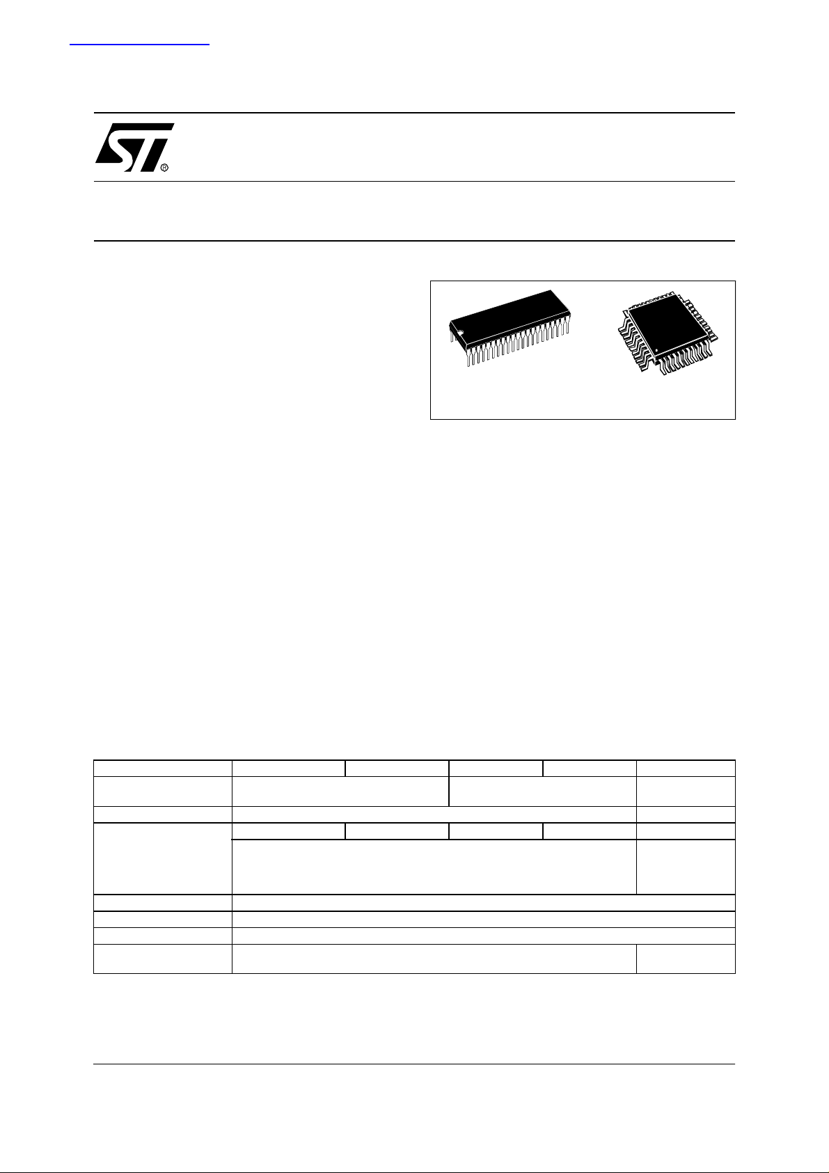
PSDIP42
compare functions
on port B
reset
modes
Windows: Real-Time Emulator, EPROM
Programming Board and Gang Programmer
compiler, source level debugger)
Device Summary
Features ST72(T/E)774 (J/S)9 ST72(T)754(J /S)9 ST72774(J/S)7 ST72754(J/S )7 ST72(T/E)734J6
Program Memory Bytes
RAM (stack) - Bytes 1K (256) 512 (256)
USB No USB USB No USB No USB
Peripherals
Operating Supply 4.0V to 5.5V supply operating range
Oscillator Frequency 12 or 24 MHz
Operating Temperature 0 to +70°C
Package CSDIP42 or PSDIP42 or TQFP44
(1) On some devices only, refer to Device Summ ary; (2) Contact Sales office for availability
(3) 8-bit ±2 LSB A/D converter ; (4) 8-bit ±4 LSB A/D converter.
ADC
3
60K 48K 32K
, 16-bit timer, I2C, DDC, TMU,Sync, PWM, LVD, Watchdog
TQFP44
10 x 10
4
, I2C,LVD,
ADC
DDC,Sync,
16-bit timer,
PWM, Watchdog
PSDIP42
CSDIP42
2
C
October 2003 1/144
1

Table of Contents
1 GENERAL DESCRIPTION . . . . . . . . . . . . . . . . . . . . . . . . . . . . . . . . . . . . . . . . . . . . . . . . . . . . . . 6
1.1 INTRODUCTION . . . . . . . . . . . . . . . . . . . . . . . . . . . . . . . . . . . . . . . . . . . . . . . . . . . . . . . . . 6
1.2 PIN DESCRIPTION . . . . . . . . . . . . . . . . . . . . . . . . . . . . . . . . . . . . . . . . . . . . . . . . . . . . . . . 7
1.3 MEMORY MAP . . . . . . . . . . . . . . . . . . . . . . . . . . . . . . . . . . . . . . . . . . . . . . . . . . . . . . . . . 10
1.4 EXTERNAL CONNECTIONS . . . . . . . . . . . . . . . . . . . . . . . . . . . . . . . . . . . . . . . . . . . . . . . 14
2 CENTRAL PROCESSING UNIT . . . . . . . . . . . . . . . . . . . . . . . . . . . . . . . . . . . . . . . . . . . . . . . . . 15
2.1 INTRODUCTION . . . . . . . . . . . . . . . . . . . . . . . . . . . . . . . . . . . . . . . . . . . . . . . . . . . . . . . . 15
2.2 MAIN FEATURES . . . . . . . . . . . . . . . . . . . . . . . . . . . . . . . . . . . . . . . . . . . . . . . . . . . . . . . 15
2.3 CPU REGISTERS . . . . . . . . . . . . . . . . . . . . . . . . . . . . . . . . . . . . . . . . . . . . . . . . . . . . . . . 15
3 CLOCKS, RESET, INTERRUPTS & LOW POWER MODES . . . . . . . . . . . . . . . . . . . . . . . . . . . 18
3.1 CLOCK SYSTEM . . . . . . . . . . . . . . . . . . . . . . . . . . . . . . . . . . . . . . . . . . . . . . . . . . . . . . . . 18
3.1.1 General Description . . . . . . . . . . . . . . . . . . . . . . . . . . . . . . . . . . . . . . . . . . . . . . . . . 18
3.1.2 Crystal Resonator . . . . . . . . . . . . . . . . . . . . . . . . . . . . . . . . . . . . . . . . . . . . . . . . . . 19
3.1.3 External Clock . . . . . . . . . . . . . . . . . . . . . . . . . . . . . . . . . . . . . . . . . . . . . . . . . . . . . 19
3.2 RESET . . . . . . . . . . . . . . . . . . . . . . . . . . . . . . . . . . . . . . . . . . . . . . . . . . . . . . . . . . . . . . . . 20
3.2.1 LVD and Watchdog Reset . . . . . . . . . . . . . . . . . . . . . . . . . . . . . . . . . . . . . . . . . . . . 20
3.2.2 External Reset . . . . . . . . . . . . . . . . . . . . . . . . . . . . . . . . . . . . . . . . . . . . . . . . . . . . . 20
3.2.3 Illegal Address Detection . . . . . . . . . . . . . . . . . . . . . . . . . . . . . . . . . . . . . . . . . . . . . 20
3.2.4 Illegal Opcode Detection . . . . . . . . . . . . . . . . . . . . . . . . . . . . . . . . . . . . . . . . . . . . . 20
3.3 INTERRUPTS . . . . . . . . . . . . . . . . . . . . . . . . . . . . . . . . . . . . . . . . . . . . . . . . . . . . . . . . . . 22
3.4 POWER SAVING MODES . . . . . . . . . . . . . . . . . . . . . . . . . . . . . . . . . . . . . . . . . . . . . . . . . 25
3.4.1 WAIT Mode . . . . . . . . . . . . . . . . . . . . . . . . . . . . . . . . . . . . . . . . . . . . . . . . . . . . . . . 25
3.4.2 HALT Mode . . . . . . . . . . . . . . . . . . . . . . . . . . . . . . . . . . . . . . . . . . . . . . . . . . . . . . . 25
3.5 MISCELLANEOUS REGISTER . . . . . . . . . . . . . . . . . . . . . . . . . . . . . . . . . . . . . . . . . . . . . 26
4 ON-CHIP PERIPHERALS . . . . . . . . . . . . . . . . . . . . . . . . . . . . . . . . . . . . . . . . . . . . . . . . . . . . . . 2 7
4.1 I/O PORTS . . . . . . . . . . . . . . . . . . . . . . . . . . . . . . . . . . . . . . . . . . . . . . . . . . . . . . . . . . . . . 27
4.1.1 Introduction . . . . . . . . . . . . . . . . . . . . . . . . . . . . . . . . . . . . . . . . . . . . . . . . . . . . . . . 27
4.1.2 Common Functional Description . . . . . . . . . . . . . . . . . . . . . . . . . . . . . . . . . . . . . . . 28
4.1.3 Port A . . . . . . . . . . . . . . . . . . . . . . . . . . . . . . . . . . . . . . . . . . . . . . . . . . . . . . . . . . . . 29
4.1.4 Port B . . . . . . . . . . . . . . . . . . . . . . . . . . . . . . . . . . . . . . . . . . . . . . . . . . . . . . . . . . . . 31
4.1.5 Port C . . . . . . . . . . . . . . . . . . . . . . . . . . . . . . . . . . . . . . . . . . . . . . . . . . . . . . . . . . . . 33
4.1.6 Port D . . . . . . . . . . . . . . . . . . . . . . . . . . . . . . . . . . . . . . . . . . . . . . . . . . . . . . . . . . . . 35
4.1.7 Register Description . . . . . . . . . . . . . . . . . . . . . . . . . . . . . . . . . . . . . . . . . . . . . . . . . 38
4.2 WATCHDOG TIMER (WDG) . . . . . . . . . . . . . . . . . . . . . . . . . . . . . . . . . . . . . . . . . . . . . . . 39
4.2.1 Introduction . . . . . . . . . . . . . . . . . . . . . . . . . . . . . . . . . . . . . . . . . . . . . . . . . . . . . . . 39
4.2.2 Main Features . . . . . . . . . . . . . . . . . . . . . . . . . . . . . . . . . . . . . . . . . . . . . . . . . . . . . 39
4.2.3 Functional Description . . . . . . . . . . . . . . . . . . . . . . . . . . . . . . . . . . . . . . . . . . . . . . . 39
4.2.4 Interrupts . . . . . . . . . . . . . . . . . . . . . . . . . . . . . . . . . . . . . . . . . . . . . . . . . . . . . . . . . 40
4.2.5 Register Description . . . . . . . . . . . . . . . . . . . . . . . . . . . . . . . . . . . . . . . . . . . . . . . . . 40
4.3 16-BIT TIMER (TIM) . . . . . . . . . . . . . . . . . . . . . . . . . . . . . . . . . . . . . . . . . . . . . . . . . . . . . . 41
4.3.1 Introduction . . . . . . . . . . . . . . . . . . . . . . . . . . . . . . . . . . . . . . . . . . . . . . . . . . . . . . . 41
4.3.2 Main Features . . . . . . . . . . . . . . . . . . . . . . . . . . . . . . . . . . . . . . . . . . . . . . . . . . . . . 41
4.3.3 Functional Description . . . . . . . . . . . . . . . . . . . . . . . . . . . . . . . . . . . . . . . . . . . . . . . 41
4.3.4 Register Description . . . . . . . . . . . . . . . . . . . . . . . . . . . . . . . . . . . . . . . . . . . . . . . . . 51
4
4.4 SYNC PROCESSOR (SYNC) . . . . . . . . . . . . . . . . . . . . . . . . . . . . . . . . . . . . . . . . . . . . . . 56
2/144
2

ST72774/ST727754/ST72734
4.4.1 Introduction . . . . . . . . . . . . . . . . . . . . . . . . . . . . . . . . . . . . . . . . . . . . . . . . . . . . . . . 56
4.4.2 Main Features . . . . . . . . . . . . . . . . . . . . . . . . . . . . . . . . . . . . . . . . . . . . . . . . . . . . . 56
4.4.3 Input Signals . . . . . . . . . . . . . . . . . . . . . . . . . . . . . . . . . . . . . . . . . . . . . . . . . . . . . . 57
4.4.4 Input Signal Waveforms . . . . . . . . . . . . . . . . . . . . . . . . . . . . . . . . . . . . . . . . . . . . . . 57
4.4.5 Output Signals . . . . . . . . . . . . . . . . . . . . . . . . . . . . . . . . . . . . . . . . . . . . . . . . . . . . . 57
4.4.6 Input Processing . . . . . . . . . . . . . . . . . . . . . . . . . . . . . . . . . . . . . . . . . . . . . . . . . . . 61
4.4.7 Output Processing . . . . . . . . . . . . . . . . . . . . . . . . . . . . . . . . . . . . . . . . . . . . . . . . . . 64
4.4.8 Analyzer Mode . . . . . . . . . . . . . . . . . . . . . . . . . . . . . . . . . . . . . . . . . . . . . . . . . . . . . 65
4.4.9 Corrector Mode . . . . . . . . . . . . . . . . . . . . . . . . . . . . . . . . . . . . . . . . . . . . . . . . . . . . 67
4.4.10Register Description . . . . . . . . . . . . . . . . . . . . . . . . . . . . . . . . . . . . . . . . . . . . . . . . . 68
4.5 TIMING MEASUREMENT UNIT (TMU) . . . . . . . . . . . . . . . . . . . . . . . . . . . . . . . . . . . . . . . 75
4.5.1 Introduction . . . . . . . . . . . . . . . . . . . . . . . . . . . . . . . . . . . . . . . . . . . . . . . . . . . . . . . 75
4.5.2 Main Features . . . . . . . . . . . . . . . . . . . . . . . . . . . . . . . . . . . . . . . . . . . . . . . . . . . . . 75
4.5.3 Functional Description . . . . . . . . . . . . . . . . . . . . . . . . . . . . . . . . . . . . . . . . . . . . . . . 75
4.5.4 Register Description . . . . . . . . . . . . . . . . . . . . . . . . . . . . . . . . . . . . . . . . . . . . . . . . . 77
4.6 USB INTERFACE (USB) . . . . . . . . . . . . . . . . . . . . . . . . . . . . . . . . . . . . . . . . . . . . . . . . . . 79
4.6.1 Introduction . . . . . . . . . . . . . . . . . . . . . . . . . . . . . . . . . . . . . . . . . . . . . . . . . . . . . . . 79
4.6.2 Main Features . . . . . . . . . . . . . . . . . . . . . . . . . . . . . . . . . . . . . . . . . . . . . . . . . . . . . 79
4.6.3 Functional Description . . . . . . . . . . . . . . . . . . . . . . . . . . . . . . . . . . . . . . . . . . . . . . . 79
4.6.4 Register Description . . . . . . . . . . . . . . . . . . . . . . . . . . . . . . . . . . . . . . . . . . . . . . . . . 80
4.6.5 Programming Considerations . . . . . . . . . . . . . . . . . . . . . . . . . . . . . . . . . . . . . . . . . 85
4.7 I²C SINGLE MASTER BUS INTERFACE (I2C) . . . . . . . . . . . . . . . . . . . . . . . . . . . . . . . . . 87
4.7.1 Introduction . . . . . . . . . . . . . . . . . . . . . . . . . . . . . . . . . . . . . . . . . . . . . . . . . . . . . . . 87
4.7.2 Main Features . . . . . . . . . . . . . . . . . . . . . . . . . . . . . . . . . . . . . . . . . . . . . . . . . . . . . 87
4.7.3 General Description . . . . . . . . . . . . . . . . . . . . . . . . . . . . . . . . . . . . . . . . . . . . . . . . . 87
4.7.4 Functional Description (Master Mode) . . . . . . . . . . . . . . . . . . . . . . . . . . . . . . . . . . . 89
4.7.5 Register Description . . . . . . . . . . . . . . . . . . . . . . . . . . . . . . . . . . . . . . . . . . . . . . . . . 91
4.8 DDC INTERFACE (DDC) . . . . . . . . . . . . . . . . . . . . . . . . . . . . . . . . . . . . . . . . . . . . . . . . . . 95
4.8.1 Introduction . . . . . . . . . . . . . . . . . . . . . . . . . . . . . . . . . . . . . . . . . . . . . . . . . . . . . . . 95
4.8.2 DDC Interface Features . . . . . . . . . . . . . . . . . . . . . . . . . . . . . . . . . . . . . . . . . . . . . . 95
4.8.3 Sig nal Description . . . . . . . . . . . . . . . . . . . . . . . . . . . . . . . . . . . . . . . . . . . . . . . . . . 97
4.8.4 I2C BUS Protocol . . . . . . . . . . . . . . . . . . . . . . . . . . . . . . . . . . . . . . . . . . . . . . . . . . . 98
4.8.5 DDC Standard . . . . . . . . . . . . . . . . . . . . . . . . . . . . . . . . . . . . . . . . . . . . . . . . . . . . . 99
4.8.6 Register Description . . . . . . . . . . . . . . . . . . . . . . . . . . . . . . . . . . . . . . . . . . . . . . . . 110
4.9 PWM/BRM GENERATOR (DAC) . . . . . . . . . . . . . . . . . . . . . . . . . . . . . . . . . . . . . . . . . . . 116
4.9.1 Introduction . . . . . . . . . . . . . . . . . . . . . . . . . . . . . . . . . . . . . . . . . . . . . . . . . . . . . . 116
4.9.2 Main Features . . . . . . . . . . . . . . . . . . . . . . . . . . . . . . . . . . . . . . . . . . . . . . . . . . . . 116
4.9.3 Functional Description . . . . . . . . . . . . . . . . . . . . . . . . . . . . . . . . . . . . . . . . . . . . . . 116
4.9.4 Register Description . . . . . . . . . . . . . . . . . . . . . . . . . . . . . . . . . . . . . . . . . . . . . . . . 121
4.108-BIT A/D CONVERTER (ADC) . . . . . . . . . . . . . . . . . . . . . . . . . . . . . . . . . . . . . . . . . . . . 123
4.10.1 Int roducti on . . . . . . . . . . . . . . . . . . . . . . . . . . . . . . . . . . . . . . . . . . . . . . . . . . . . . . 123
4.10.2Main Features . . . . . . . . . . . . . . . . . . . . . . . . . . . . . . . . . . . . . . . . . . . . . . . . . . . . 123
4.10.3 F unct ional Description . . . . . . . . . . . . . . . . . . . . . . . . . . . . . . . . . . . . . . . . . . . . . . 123
4.10.4Low Power Mode . . . . . . . . . . . . . . . . . . . . . . . . . . . . . . . . . . . . . . . . . . . . . . . . . 124
4.10.5Interrupts . . . . . . . . . . . . . . . . . . . . . . . . . . . . . . . . . . . . . . . . . . . . . . . . . . . . . . . . 124
4.10.6Register Description . . . . . . . . . . . . . . . . . . . . . . . . . . . . . . . . . . . . . . . . . . . . . . . . 125
5 INSTRUCTION SET . . . . . . . . . . . . . . . . . . . . . . . . . . . . . . . . . . . . . . . . . . . . . . . . . . . . . . . . . 126
5.1 ST7 ADDRESSING MODES . . . . . . . . . . . . . . . . . . . . . . . . . . . . . . . . . . . . . . . . . . . . . . 126
3/144

ST72774/ST727754/ST72734
5.1.1 Inherent . . . . . . . . . . . . . . . . . . . . . . . . . . . . . . . . . . . . . . . . . . . . . . . . . . . . . . . . . 127
5.1.2 Imme diate . . . . . . . . . . . . . . . . . . . . . . . . . . . . . . . . . . . . . . . . . . . . . . . . . . . . . . . 127
5.1.3 Direct . . . . . . . . . . . . . . . . . . . . . . . . . . . . . . . . . . . . . . . . . . . . . . . . . . . . . . . . . . . 127
5.1.4 Indexed (No Offset, Short, Long) . . . . . . . . . . . . . . . . . . . . . . . . . . . . . . . . . . . . . . 127
5.1.5 Indirect (Short, Long) . . . . . . . . . . . . . . . . . . . . . . . . . . . . . . . . . . . . . . . . . . . . . . . 127
5.1.6 Indirect Indexed (Short, Long) . . . . . . . . . . . . . . . . . . . . . . . . . . . . . . . . . . . . . . . . 128
5.1.7 Relative mode (Direct, Indirect) . . . . . . . . . . . . . . . . . . . . . . . . . . . . . . . . . . . . . . . 128
5.2 INSTRUCTION GROUPS . . . . . . . . . . . . . . . . . . . . . . . . . . . . . . . . . . . . . . . . . . . . . . . . 129
6 ELECTRICAL CHARACTERISTICS . . . . . . . . . . . . . . . . . . . . . . . . . . . . . . . . . . . . . . . . . . . . . 132
6.1 POWER CONSIDERATIONS . . . . . . . . . . . . . . . . . . . . . . . . . . . . . . . . . . . . . . . . . . . . . 133
6.2 AC/DC ELECTRICAL CHARACTERISTICS . . . . . . . . . . . . . . . . . . . . . . . . . . . . . . . . . . 134
7 GENERAL INFORMATION . . . . . . . . . . . . . . . . . . . . . . . . . . . . . . . . . . . . . . . . . . . . . . . . . . . . 139
7.1 PACKAGE MECHANICAL DATA . . . . . . . . . . . . . . . . . . . . . . . . . . . . . . . . . . . . . . . . . . . 139
8 ORDERING INFORMATION . . . . . . . . . . . . . . . . . . . . . . . . . . . . . . . . . . . . . . . . . . . . . . . . . . . 141
8.1 TRANSFER OF CUSTOMER CODE . . . . . . . . . . . . . . . . . . . . . . . . . . . . . . . . . . . . . . . . 141
4/144

Revision follow-up
Changes applied since version 4.0
Version 4.0 March 2001
Page 1:Addition of 72T774 (32KOTP).
Addition of 60K/48K ROM for ST72754
Deletion of table “ device summary”, replaced with cross reference to table 36 on page 147.
page 13 - addition of section 1.4. external connections
Version 4.1 July 2001
Initial format reapplied, text and related figures in the same page.
Table “Device summary” reinserted in cover page and updated.
Update of table 36: ordering information (p143)
Version 4.2 July 2001
Cover - addition of feature about system protection added,
table for device summary: addition of stack values
page 9 - figure 3: replaced 1KByte with 512 Bytes + notes about opcode fetch and HALT
mode
page 10 - table: CR replaced by WDGCR
TIM replaced with Timer and WDG replaced with Watchdog
page 115 - EDF register: addition of “read from RAM”, EDE: few changes
page 135 - Note 1 replaced, note 2 added SUSpend mode limitation..
Whole document: all mentions of HALT mode either deleted or rewritten.
Version 4.3 October 2001
p140, chapter 8, section 8.1code for unused bytes ( FFh) replaced with
page 141- update of table 36 “Ordering information”
page 142 - list of available devices updated
page 114 - DDC DCR register: bit 5 = 1, text “or read from RAM” deleted
Version 4.3 November 2001
page 10, one adddress corrected in the figure 3 “memory map”: 0400h
page 14: addition of mandatory 1K resistor (text and figure)
ST72774/ST727754/ST72734
9Dh (opcode for NOP)
5/144
3
ST72774/ST727754/ST72734
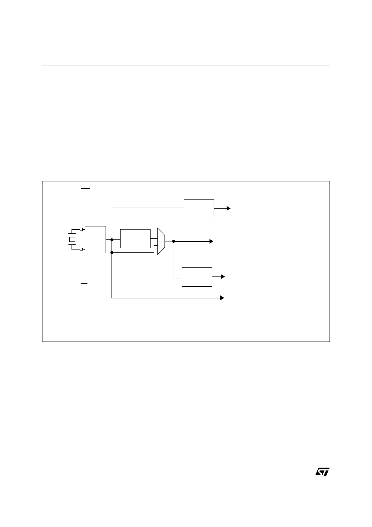
1 GENERAL DESCRIPTION
1.1 INTRODUCTION
The ST72774, ST72754 and ST72734 are
HCMOS microcontroller units (MCU) from the
ST727x4 family with dedicated peripherals for
Monitor applications.
They are based around an industry standard 8-bit
core and offer an enhanced instruction set. The
processor runs with an external clock at 12 or 24
MHz with a 5V supply. Due to the fully static design
of this device, operation do wn to DC is possible.
Under software control the ST727x4 can be placed
in WAIT mode thus reducing p ower consumpt ion.
The HALT mode is no longer available.
The enhanced instruction set and addressing
modes afford real programming potential. Illegal
opcodes are patched and lead to a reset.
Figure 1. ST727x4 Block Diagram
Up to 60K Bytes
ROM/OTP/EPROM
Up to 1K Bytes
RAM
In addition to standard 8-bit data management the
ST7 features true bit manipulation, 8x8 unsigned
multiplication and indirect addressing modes.
The device includes an on-chip oscillator, CPU,
System protection aga inst illeg al add re ss j umps,
Sync Processor for video timing & Vfback analysis,
up to 60K Program Mem ory, up to 1K RAM, US B/
DMA, a Timing Measurement Unit, I/O, a timer with
2 input captures and 2 output compares, a 4channel Analog to Digital Converter, DDC, I
Single Master, W atchdog Reset, and ei ght 10-bit
PWM/BRM outputs for analog DC control of
external functions.
PA0/OCMP1
PA1
PORT A
PORT B
ADC
I2C
PA2/VSYNCI2
PA3-PA6
PA7/BLANKOUT
PB6-PB7/AIN2-AIN 3/ PWM1- PWM2
PB4-PB5/AIN0-AIN1
PB3/SDAI
PB2/SCLI
2
C
RESET
OSCIN
OSCOUT
V
V
6/144
DD
SS
CONTROL
8-BIT CO RE
ALU
WATCHDOG
Mode
3
:
OSC
Selection
POWER SUPPLY
DDC
ADDRESS AND DATA BUS
USB
PORT D
TIMER
SYNC
PROCESSOR
TMU
PORT C
DAC (PWM)
PB1/SDAD
PB0/SCLD
USBVCC
USBDP
USBDM
PD0/VSYNCO
PD1/HSYNCO
PD2/CSYNCI
PD3/ITA/VFBACK
PD4/ITB
PD5/HFBACK
PD6/CLAMPOUT
VSYNCI
HSYNCI
PC0/HSYNCDIV
PC1/AV
PC2-PC7/PWM3-PWM8
3
1.2 PIN DESCRI PTION
Figure 2. 44-pin TQFP and 42-Pin SDIP Package Pinouts
PC1 / AV
PC0 / HSYNCDIV
PA0 / O C MP1
PWM7 / PC6
PWM8 / PC7
PWM2 / AIN3 / PB7
PWM1 / AIN2 / PB6
AIN1 / PB5
AIN0 / PB4
NC
V
DD
USBVCC
USBDM
USBDP
PC5 / PWM6
PC4 / PWM5
PC3 / PWM4
PC2 / PWM3
44 43 42 41 40 39 38 37 36 35 34
1
2
3
4
5
6
7
8
9
10
11
12 13 14 15 16 17 18 19 20 21 22
ss
V
TEST / VPPRESET
PA1
ST72774/ST727754/ST72734
PA2/VSYNCI2
PA3
33
PA4
32
PA5
31
PA6
30
OSCIN
29
OSCOUT
28
PA7 / BLANKO UT
27
PB3 / SDAI
26
PB2 / SCLI
25
PB1 / SDAD
24
NC
23
HSYNCDIV / PC0
AV / PC1
PWM3 / PC2
PWM4 / PC3
PWM5 / PC4
PWM6 / PC5
PWM7 / PC6
PWM8 / PC7
PWM2 / AIN3 / PB7
PWM1 / AIN2 / PB6
AIN1 / PB5
AIN0 / PB4
V
DD
USBVCC
USBDM
USBDP
V
SS
HSYNCI
VSYNCI
VSYNCO / PD0
HSYNCO / PD1
VSYNCI
HSYNCI
VSYNCO / PD0
HSYNCO / PD1
1
2
3
4
5
6
7
8
9
10
11
12
13
14
15
16
17
18
19
20
21
ITB / PD4
CSYNCI / PD2
VFBACK / IT A /PD3
42
41
40
39
38
37
36
35
34
33
32
31
30
29
28
27
26
25
24
23
22
SCLD / PB0
HFBACK / PD5
CLAMPOUT / PD6
PA0 / OCMP1
TEST / V
RESET
PA1
PA2/VSYNCI2
PA3
PA4
PA5
PA6
OSCIN
OSCOUT
PA7 / BLANKOUT
PB3 / SDAI
PB2 / SCLI
PB1 / SDAD
PB0 / SCLD
PD6 / CLAMPOUT
PD5 / HFBACK
PD4 / ITB
PD3 / ITA / VFBACK
PD2 / CSYNCI
PP
NC = Not connected
7/144
3
ST72774/ST727754/ST72734
PIN DESCRIPTION (Cont’d)
RESET:
Bidirectional. This active low signal forces
the initialization of the MCU. This event is the top
priority non maskable interrupt. This pin is
switched low when the Watchdog has triggered or
V
is low. It can be used to reset external
DD
peripherals.
OSCIN/OSCOUT: Input/Output Oscillator pin.
These pins connect a pa rallel-resonant crystal, or
an external sou rc e to the on -c h ip o s cilla t o r.
TEST/V
: Input. EPROM programming voltage.
PP
This pin must be held low during normal operating
modes.
V
: Power supply voltage (4.0V-5.5V)
DD
V
: Digital Ground.
SS
Alter nate Funct ions: several pins of the I/O ports
assume software programmable alternate
functions as shown in the pin description
Table 1. ST727x4 Pin Description
Pin No.
Pin Name
SDIP42
TQFP44
39 1 PC0/HSYNCDIV I/O Port C0 or HSYNCDIV output (HSYNCO divided by 2)
40 2 PC1/AV I/O Port C1 or “Active Video” input
41 3 PC2/PWM3 I/O Port C2 or 10-bit PWM/BRM output 3
42 4 PC3/PWM4 I/O Port C3 or 10-bit PWM/BRM output 4
43 5 PC4/PWM5 I/O Port C4 or 10-bit PWM/BRM output5
44 6 PC5/PWM6 I/O Port C5 or 10-bit PWM/BRM output 6
1 7 PC6/PWM7 I/O Port C6 or 10-bit PWM/BRM output 7
2 8 PC7/PWM8 I/O Port C7 or 10-bit PWM/BRM output 8
3 9 PB7/AIN3/PWM2 I/O
4 10 PB6/AIN2/PWM1 I/O
5 11 PB5/AIN1 I/O Port B5 or ADC analog input 1
6 12 PB4/AIN0 I/O Port B4 or ADC analog input 0
813V
9 14 USBVCC S USB power supply (output 3.3V +/- 10%)
10 15 USBDM I/O USB bidirectional data Must be tied to ground
11 16 USBDP I/O USB bidirectional data
12 17 V
13 18 HSYNCI I SYNC horizontal synchronisation input
14 19 VSYNCI I SYN C vertical synch ronis ation input
15 20 PD0/VSYNCO I/O Port D0 or SYNC vertical synchronisation output
16 21 PD1/HSYNCO I/O Port D1 or SYNC horizontal synchronisation output
17 22 PD2/CSYNCI I/O Port D2 or SYNC composite synchronisation input
DD
SS
Type
Port B7 or ADC analog input 3 or 10-bit PWM/BRM
output 2
Port B6 or ADC analog input 2 or 10-bit PWM/BRM
output 1
S Supply (4.0V - 5.5V)
S Ground 0V
Description Remarks
For analog controls,
after external filtering
for devices without
USB peripheral
TTL levels
Refer to Figure 16
TTL levels with pull-up
(SYNC input)
8/144
3
Pin No.
ST72774/ST727754/ST72734
Pin Name
SDIP42
TQFP44
18 23 PD3/VFBACK/ITA I/O
19 24 PD4/ITB I/O Port D4 or Interrupt falling edge detector input B
20 25 PD5/HFBACK I/O Port D5 or SYNC horizontal flyback input
21 26 PD6/CLAMPOUT I/O Port D6 or SYNC clamping/ MOIRE output
22 27 PB0/SCLD I/O Port B0 or DDC serial clock
24 28 PB1/SDAD I/O Port B1 or DDC serial data
25 29 PB2/SCLI I/O Port B2 or I2C serial clock
26 30 PB3/SDAI I/O Port B3 or I2C serial data
27 31 PA7/BLANKOUT I/O Port A7 or SYNC blanking output
28 32 OSCOUT O Oscillator output
29 33 OSCIN I Oscillator input
30 34 PA6 I/O Port A6
31 35 PA5 I/O Port A5
32 36 PA4 I/O Port A4
33 37 PA3 I/O Port A3
34 38 PA2/VSYNCI2 I/O Port A2 or SYNC vertical synchronisation input 2 DDC1 only
35 39 PA1 I/O Port A1
36 40 RESET
37 41 TEST/V
38 42 PA0/OCMP1 I/O Port A0 or TIMER output compare 1
PP
Type
Port D3 or SYNC Vertical flyback input or interrupt falling edge detector input A
I/O Reset pin Active low
Test mode pin or EPROM programming voltage. This
S
pin should be tied low in user mode.
Description Remarks
Refer to Figure 16 and
Table 11 Port D Description
Refer to Table 11 Port
D Description
TTL levels with pull-up
(SYNC input)
9/144
ST72774/ST727754/ST72734
1.3 MEMORY MA P
Figure 3. Me m ory Map
0000h
005Fh
0060h
03FFh
0400h
0FFFh
1000h
4000h
8000h
FFDFh
FFE0h
FFFFh
HW Registers
(see Table 2)
512 Bytes RAM
1 Kbyte RAM
Reserved
60 Kbytes
ROM/EPROM
48 Kbytes
32 Kbytes
Interrupt & Reset Vectors *
(see Table 3)
0060h
0100h
01FFh
0060h
0100h
01FFh
0200h
03FFh
Short Addressing
RAM (zero page)
256 Bytes Stack/
16-bit Addressing RAM
Short Addressing
RAM (zero page)
256 Bytes Stack/
16-bit Addressing RAM
16-bit Addressing
RAM
512 Bytes
any opcode fetch in those areas is considered as illegal and generates a reset
(*) this block only contains addresses of interrupts and reset routines, no opcode is run from this block
10/144
MEMORY MAP (Cont’d)
Table 2. Hardware Register Mem ory Map
ST72774/ST727754/ST72734
Address Block Register Label Register Name
0000h
0001h
0002h
0003h
0004h
0005h
0006h
0007h
0008h Watchdog WDGCR Watchdog Control Register 7Fh R/W
0009h MISCR Miscellaneous Register 10h R/W
000Ah
000Bh
000Ch
000Dh
000Eh
000Fh
00010h
0011h
0012h
0013h
0014h
0015h
0016h
0017h
0018h
0019h
001Ah
001Bh
001Ch
001Dh
001Eh
001Fh
0020h
to
0024h
ADC
DDC1/2B
TMU
Timer
PADR
PADDR
PBDR
PBDDR
PCDR
PCDDR
PDDR
PDDDR
ADCDR
ADCCSR
DDCDCR
DDCAHR
TMUCSR
TMUT1CR
TMUT2CR
TIMCR2
TIMCR1
TIMSR
TIMIC1HR
TIMIC1LR
TIMOC1HR
TIMOC1LR
TIMCHR
TIMCLR
TIMACHR
TIMACLR
TIMIC2HR
TIMIC2LR
TIMOC2HR
TIMOC2LR
Port A Data Register
Port A Data Direction Register
Port B Data Register
Port B Data Direction Register
Port C Data Register
Port C Data Direction Register
Port D Data Register
Port D Data Direction Register
ADC Data Register
ADC Control Status register
DDC1/2B Control Register
DDC1/2B Address Pointer High Register
TMU control status register
TMU T1 counter register
TMU T2 counter register
Timer Control Register 2
Timer Control Register 1
Timer Status Register
Timer Input Capture 1 High Register
Timer Input Capture 1 Low Register
Timer Output Compare 1 High Register
Timer Output Compare 1 Low Register
Timer Counter High Register
Timer Counter Low Register
Timer Alternate Counter High Register
Timer Alternate Counter Low Register
Timer Input Capture 2 High Register
Timer Input Capture 2 Low Register
Timer Output Compare 2 High Register
Timer Output Compare 2 Low Register
Reserved Area (5 bytes)
Status
00h
00h
00h
00h
00h
00h
00h
00h
00h
00h
00h
xxh
FCh
FFh
FFh
00h
00h
00h
xxh
xxh
80h
00h
FFh
FCh
FFh
FCh
xxh
xxh
80h
00h
Reset
R/W
R/W
R/W
R/W
R/W
R/W
R/W
R/W
Read only
R/W
R/W
R/W
R/W
Read only
Read only
R/W
R/W
Read only
Read only
Read only
R/W
R/W
Read only
R/W
Read only
R/W
Read only
Read only
R/W
R/W
Remarks
11/144
ST72774/ST727754/ST72734
Address Block Register Label Register Name
0025h
0026h
0027h
0028h
0029h
002Ah
002Bh
002Ch
002Dh
002Eh
002Fh
0030h
0031h
0032h
0033h
0034h
0035h
0036h
0037h
0038h
0039h
003Ah
003Bh
003Ch
003Dh
003Eh
003Fh Reserved Area (1 byte)
0040h
0041h
0042h
0043h
0044h
0045h
0046h
0047h
0048h
to
004Fh
USB
PWM
SYNC
USBPIDR
USBDMAR
USBIDR
USBISTR
USBIMR
USBCTLR
USBDADDR
USBEP0RA
USBEP0RB
USBEP1RA
USBEP1RB
USBEP2RA
USBEP2RB
PWM1
BRM21
PWM2
PWM3
BRM43
PWM4
PWM5
BRM65
PWM6
PWM7
BRM87
PWM8
PWMCR
SYNCCFGR
SYNCMCR
SYNCCCR
SYNCPOLR
SYNCLATR
SYNCHGENR
SYNCVGENR
SYNCENR
USB PID Register
USB DMA address Register
USB Interrupt/DMA Register
USB Interrupt Status Register
USB Interrupt Mask Register
USB Control Register
USB Device Address Register
USB Endpoint 0 Register A
USB Endpoint 0 Register B
USB Endpoint 1 Register A
USB Endpoint 1 Register B
USB Endpoint 2 Register A
USB Endpoint2 Register B
10 BIT PWM / BRM
PWM output enable register
SYNC Configuration Register
SYNC Multiplexer Register
SYNC Counter Register
SYNC Polarity Register
SYNC Latch Register
SYNC H Sync Generator Register
SYNC V Sync Generator Register
SYNC Processor Enable Register
Reserved Area (8 bytes)
Reset
Status
XXh
XXh
XXh
00h
00h
xxxx 0110
00h
0000 xxxx
80h
0000 xxxx
0000
xxxx0000
0000
xxxx0000
80h
00h
80h
80h
00h
80h
80h
00h
80h
80h
00h
80h
00h
00h
20h
00h
08h
00h
00h
00h
C3h
Remarks
Read only
R/W
R/W
R/W
R/W
R/W
R/W
R/W
R/W
R/W
R/W
R/W
R/W
R/W
R/W
R/W
R/W
R/W
R/W
R/W
R/W
R/W
R/W
R/W
R/W
R/W
R/W
R/W
R/W
R/W
R/W
R/W
R/W
R/W
12/144
ST72774/ST727754/ST72734
Address Block Register Label Register Name
0050h
0051h
0052h
0053h
0054h
0055h
0056h
0057h
0058h
0059h
005Ah
005Bh
005Ch
005Dh
005Eh
005Fh
DDC/CI
I2C
DDCCR
DDCSR1
DDCSR2
DDCOAR
DDCDR
I2CDR
I2CCCR
I2CSR2
I2CSR1
I2CCR
DDC/CI Control Register
DDC/CI Status Register 1
DDC/CI Status Register 2
Reserved
DDC/CI (7 Bits) Slave address Register
Reserved
DDC/CI Data Register
Reserved Area (2 bytes)
I2C Data Register
Reserved
Reserved
2
C Clock Control Register
I
2
C Status Register 2
I
2
C Status Register 1
I
2
C Control Register
I
Reset
Status
00h
00h
00h
00h
00h
00h
00h
00h
00h
00h
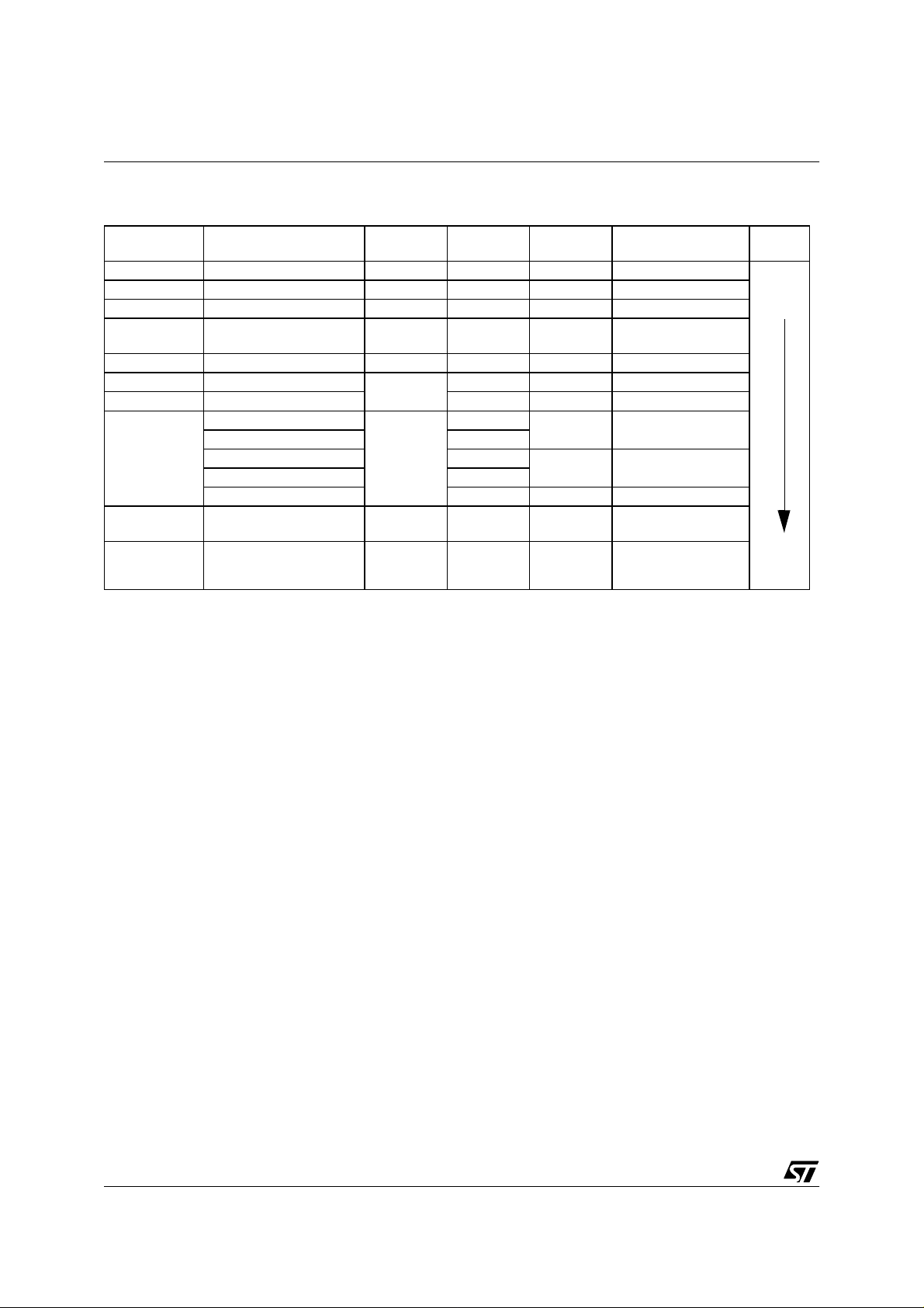
Table 3. Interrupt Vector Map
Vector Address Description Remarks
FFE0-FFE1h
FFE2-FFE3h
FFE4-FFE5h
FFE6-FFE7h
FFE8-FFE9h
FFEA-FFEBh
FFEC-FFEDh
FFEE-FFEFh
FFF0-FFF1h
FFF2-FFF3h
FFF4-FFF5h
FFF6-FFF7h
FFF8-FFF9h
FFFA-FFFBh
FFFC-FFFDh
FFFE-FFFFh
Timer Overflow interrupt vector
Timer Output Compare interrupt vector
Timer Input Capture interrupt vector
ITA falling edge interrupt vector
ITB falling edge interrupt vector
DDC1/2B interrupt vector
USB End Suspend interrupt vector
TRAP (software) interrupt vector
Not used
Not used
Not used
USB interrupt vector
Not used
I2C interrupt vector
DDC/CI interrupt vector
RESET vector
Internal Interrupts
External Interrupts
Internal Interrupt
CPU Interrupt
Remarks
R/W
Read only
Read only
R/W
R/W
R/W
R/W
Read only
Read only
R/W
13/144
ST72774/ST727754/ST72734
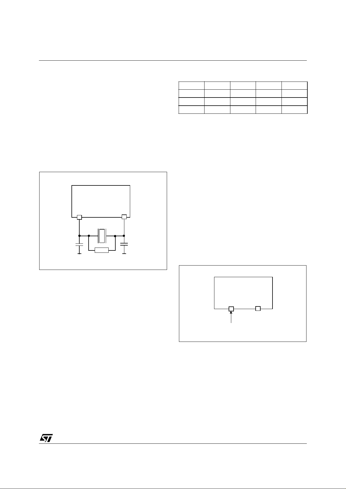
1.4 External connections
The following figure shows the recom mended external connections for the device.
The V
pin is only used for programming OTP
PP
and EPROM devices and must be tied to ground in
user mode.
The 10 nF and 0. 1 µF decoupling capacitors on
the power supply lines are a suggested EMC performance/cost tradeoff.
Figure 4. Recommended Extern al Connec tions
V
DD
EXTERNAL RESET CIRCUIT
10nF
V
DD
0.1µF
0.1µF
+
4.7K
The external reset network (including the mandatory 1K serial resistor) is inten ded to protect the
device against parasitic resets, espec ially in noisy
environments.
Unused I/Os shoul d be t ied hi gh to av oid any unnecessary power consumption on floating lines.
An alternative solution is to program the unused
ports as inputs with pull-up.
V
PP
V
0.1µF
1K
DD
V
SS
RESET
14/144
See
Clocks
Section
Or configure unused I/O ports
by software as input with pull-up
V
10K
DD
OSCIN
OSCOUT
Unused I/O
2 CENTRAL PRO CESSING UNIT
ST72774/ST727754/ST72734
2.1 INTRODUCTION
This CPU has a full 8-bit architecture and contains
six internal registers allowing efficient 8-bit data
manipulation.
2.2 MAIN FEATURES
■ 63 basic instructions
■ Fast 8-bit by 8-bit multiply
■ 17 main addressing modes
■ Two 8-bit index registers
■ 16-bit stack pointer
■ Low power modes
■ Maskable hardware interrupts
■ Non-maskable software interrupt
2.3 CPU REGISTERS
The 6 CPU registers shown in Figure 5 are not
present in the memory mapping and are accessed
by specific instructions.
Accumulator (A)
Figure 5. CPU Registers
70
RESET VALUE = XXh
70
RESET VALUE = XXh
70
RESET VALUE = XXh
The Accumulator is an 8-bit general purpose
register used to hold operands and the results of
the arithmetic and logic calculations and to
manipulate data.
Index Registers (X and Y)
In indexed addressing modes, these 8-bit registers
are used to create either effective addresses or
temporary storage areas for data manipulation.
(The Cross-Assembler generates a precede
instruction (PRE) to indicate that the following
instruction refers to the Y register.)
The Y register is not affected by the interrupt
automatic procedures (not pushed to and pop ped
from the stack).
Program Cou nt er (P C )
The program counter is a 16-bit register containing
the address of the next instruction to be executed
by the CPU. It is made of two 8-bit registers PCL
(Program Counter Low which is the LSB) and PCH
(Program Counter High which is the MSB).
ACCUMULATOR
X INDEX REGISTER
Y INDEX REGISTER
15 8
RESET VALUE = RESET VECTOR @ FFFEh-FFFFh
15
RESET VALUE = STACK HIGHER ADDRESS
PCH
RESET VALUE =
7
70
1C11HI NZ
1X11X1XX
70
8
PCL
0
PROGRAM COUNTER
CONDITION CODE REGISTER
STACK POINTER
X = Undefined Value
15/144

ST72774/ST727754/ST72734
CPU REGISTERS (Cont’d)
CONDITION CODE REGISTER (CC)
Read/Write
Reset Value: 111x1xxx
70
enter it and reset by the IRET instruction at the end
of the interrupt routine. If the I bit is cleared by
software in the interrupt routine, pending interrupts
are serviced regardless of the pri ority level of the
current interrupt routine.
111HINZC
The 8-bit Condition Code register contains the
interrupt mask and four flags representative of the
result of the instruction just executed. This register
can also be handled by the PUSH and POP
instructions.
These bits can be individually tested and/or
controlled by specific instructions.
Bit 4 = H
Half carry
.
This bit is set by hardware when a carry occurs
between bits 3 and 4 of the ALU during an ADD or
ADC instruction. It is reset by hardware during the
same instructions.
0: No half carry has occurred.
1: A half carry has occurred.
This bit is tested using the JRH or JRNH
instruction. The H bit is useful in B CD arithmetic
subroutines.
Bit 2 = N
Negative
.
This bit is set and cleared by hardware. It is
representative of the result sign of the last
arithmetic, logical or data manipulation. It is a copy
of the 7
th
bit of the result.
0: The result of the last operation is positive or null.
1: The result of the last operation is negative
(i.e. the most significant bit is a logic 1).
This bit is accessed by the JRMI and JRPL
instructions.
Bit 1 = Z
Zero
.
This bit is set and cleared by hardware. This bit
indicates that the result of the last arithmetic,
logical or data manipulation is zero.
0: The result of the last operation is different from
zero.
1: The result of the last operation is zero.
This bit is accessed by the JREQ and JRNE test
instructions.
Bit 3 = I
Interrupt mask
.
This bit is set by hardware when entering in
interrupt or by software to disable all interrupts
except the TRAP software interrupt. This bit is
cleared by software.
0: Interrupts are enabled.
1: Interrupts are disabled.
This bit is controlled by the RIM, SIM and IRET
instructions and is tested by the JRM and JRNM
instructions.
Note: Interrupts requested while I is set are
latched and can be processed whe n I is cleared.
By default an interrupt routine is not in terruptable
because the I bit is set by hardware when you
16/144
Bit 0 = C
Carry/borrow.
This bit is set and cleared by hardware and
software. It indicates an overflow or an underflow
has occurred during the last arithmetic operation.
0: No overflow or underflow has occurred.
1: An overflow or underflow has occurred.
This bit is driven by th e SCF and RCF instructions
and tested by the JRC and JRNC instructions. It is
also affected by the “bit test and branch”, shift and
rotate instructions.
ST72774/ST727754/ST72734
CPU REGISTERS (Cont’d)
Stack Pointer (SP)
Read/Write
Reset Value: 01 FFh
15 8
00000001
70
The least significant byte of the Stack Pointer
(called S) can be directly accessed by a LD
instruction.
Note: When the lower limit is exceeded, the Stack
Pointer wraps around to the stack upper limit,
without indicating the stack overflow. The
previously stored information is then overwritten
and therefore lost. The stack also wraps in case of
an underflow.
SP7 SP6 SP5 SP4 SP3 SP2 SP1 SP0
The Stack Pointer is a 16-bit register which is
always pointing to the next free location in the
stack. It is then decremented after data has been
pushed onto the stack and incremented before
data is popped from the stack (see Figure 6).
Since the stack is 256 bytes deep, the most
significant byte is forced by ha rd ware. Fol lowing
an MCU Reset, or after a Reset Stack Pointer
instruction (RSP), the Stack Pointer contains its
reset value (the SP7 to SP0 bits are set) which is
the stack higher address.
Figure 6. Stack Manipulation Example
@ 0100h
SP
@ 01FFh
CALL
Subroutine
PCH
PCL
Interrupt
event
SP
SP
CC
A
X
PCH
PCL
PCH
PCL
PUSH Y POP Y IRET
Y
CC
A
X
PCH
PCL
PCH
PCL
The stack is used to save the return address
during a subroutine call and the CPU context
during an interrupt. The user may also directly
manipulate the stack b y means of the PU SH and
POP instructions. In the case of an in terrupt, the
PCL is stored at the first location pointed to by the
SP. Then the other registers are stored in the next
locations as shown in Figure 6.
– When an interrupt is received, the SP is decre-
mented and the context is pushed on the stack.
– On return from interrupt, the SP is incremented
and the context is popped from the stack.
A subroutine call occupies two locations and an
interrupt five locations in the stack area.
RET
or RSP
SP
CC
A
X
PCH
PCL
PCH
PCL
SP
PCH
PCL
SP
Stack Higher Address = 01FFh
Stack Lower Address =
0100h
17/144
ST72774/ST727754/ST72734
3 CLOCKS, RESET, INTERRUPTS & LOW POWER MODES
3.1 CLOCK SYSTEM
3.1.1 General Description
The MCU accepts either a cry stal or an external
clock signal to drive the internal oscillator. The
internal clock (CPU CLK running at f
CPU
) is
derived from the external oscillator frequency
), which is divided by 3. Depending on the
(f
OSC
external quartz or clock frequency, a division factor
of 2 is optionally added to generate the 12 MHz
clock for the Sync Processor (clamp function) as
Figure 7. Clock divider chain
OSC
12 MHz
or
%2
FAST
24MHz
shown in Figure 7 and a second divider by 2 for the
6MHz USB clock.
The CPU clock is used also as clock for the
ST727x4 peripherals.
Note: In the Sync processor, an additional divider
by two is added in fast mode (same external timing
for this peripheral).
f
: 4 or 8 MHz
%3
CPU
(CPU and peripherals)
12 MHz
(Sync processor Clampout signal)
%2
6 MHz
(USB)
FAST=1 for 24 M H Z os c illator FAST=0 for 12 MHz osc il lat o r
18/144
12 MHz
or
24MHz
(TMU)
4
CLOCK SYSTEM (Cont’d)
3.1.2 Crystal Resonator
The internal oscillat or is designed to operate with
an AT-cut parallel resonant quartz crystal
resonator in the frequency range specified for f
osc
The circuit shown in Figure 8 is recommended
when using a crystal, and Table 4, “.
Recommended Crystal Values,” on page 19 lists
the recommended capacitance and feedback
resistance values. The crystal and associated
components should be mounted as close as
possible to the input pins in order to minimize
output distortion and start-up stabilization time.
Figure 8. Crystal/Ceramic Resonator
CRYSTAL CLOCK
OSCIN OSCOUT
C
L1
C
L2
ST72774/ST727754/ST72734
Table 4
.
Legend:
C
OSCIN and OSCOUT (the value includes the
external capacitance tied to the pin plus the
parasitic capacitance of the board and of the
device).
R
the quartz allowed.
Note: The tables are relative t o the quart z crystal
only (not ceramic resonator).
3.1.3 External Clock
An external clock should be appli ed to t he O SCIN
input with the OSCOUT pin not connected as
shown in Figure 9. The Crystal clock specifications
do not apply when using an external clock input.
The equivalent spe cification of the external clock
source should be used.
. Recomm en de d Crystal Values
24 Mhz Unit
R
SMAX
C
L1
C
L2
, CL2 = Maximum total capacitance on pins
L1
= Maximum series parasitic resistance of
SMAX
70 25 20 Ohms
22 47 56 pf
22 47 56 pf
*Recommended for oscillator stability
1M*
Figure 9. External Clock Source Connections
OSCIN
EXTERNAL
CLOCK
OSCOUT
NC
19/144
ST72774/ST727754/ST72734
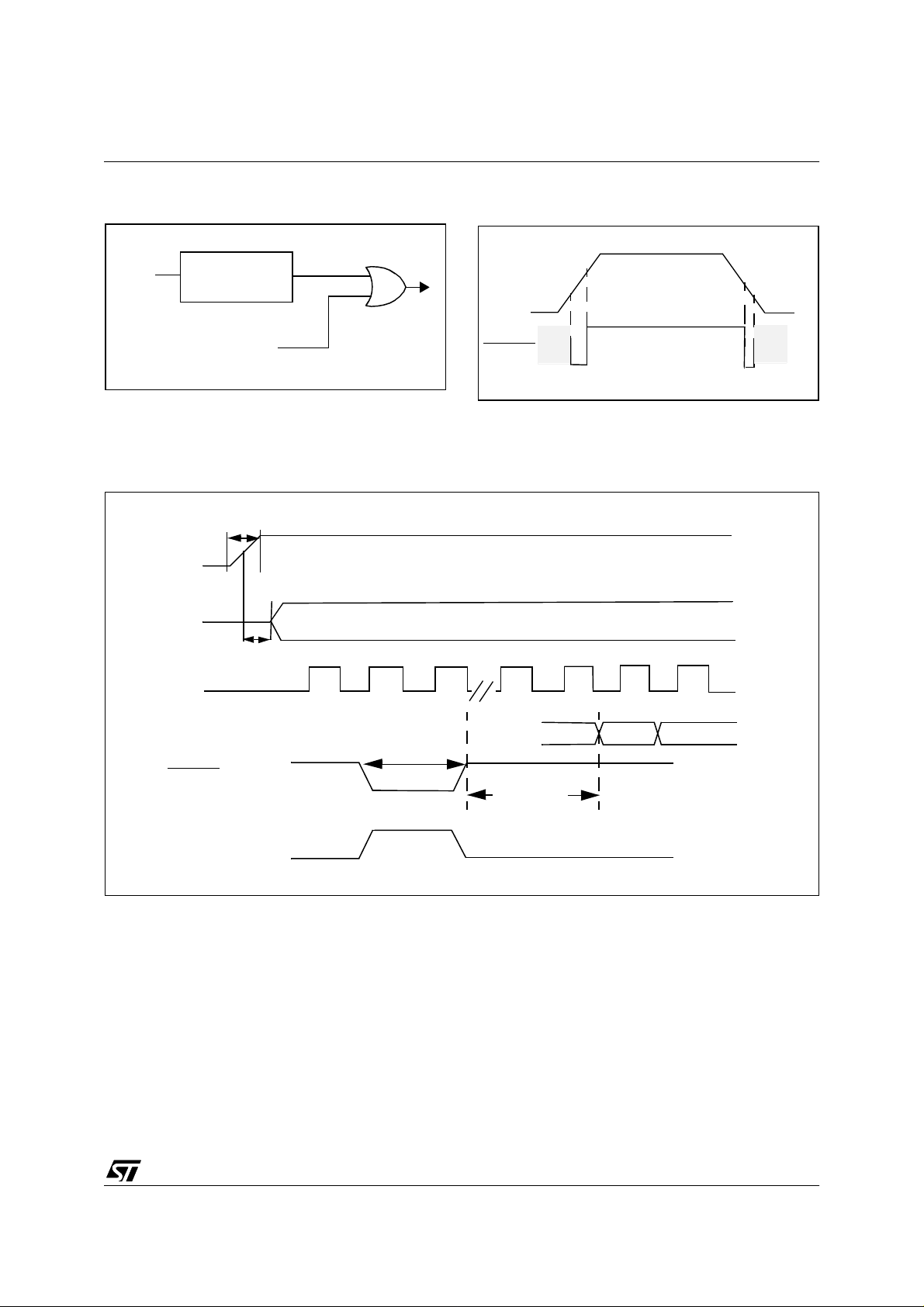
3.2 RESET
The Reset procedure is used to provide an orderly
software start-up or to quit low powe r modes.
Five conditions generate a reset:
■ LVD,
■ watchdog,
■ external pulse at the RESET pin,
■ illegal address,
■ illegal opcode.
A reset causes the reset vector to be fetched from
addresses FFFEh and FFFFh in order to be loaded
into the PC and with program execution starting
from this point.
An internal circuitry provides a 4096 CPU clock
cycle delay from the time that the oscillator
becomes active.
3.2.1 LVD and Watchdog Reset
The Low Voltage Detector (LVD) generates a reset
when V
when
is active only when V
is below V
DD
is falling (refer to Figure 11). This circuitry
VDD
when VDD is ri sing or V
TRH
is above V
DD
TRM.
TRL
During LVD Reset, the RESET pin is held low, thus
permitting the MCU to reset other devices.
When a watchdog reset occurs, the RESET
pin is
pulled low permitting the MCU to reset other
devices as when Power on/off (Figure 10).
3.2.2 External Reset
The external reset is an active low input signal
applied to the RESET pin of the MCU.
As shown in Figure 12, the RESET
signal must
remain low for 1000ns.
An internal Schmitt trigger at the RESET
pin is
provided to improve noise immunity.
3.2.3 Illegal Address Detection
An opcode fetch from an illegal address (refer to
Figure 3) generates an illegal address reset.
Program execution at those addresses is
forbidden (especially to protect page 0 registers
against spurious accesses).
3.2.4 Illegal Opcode Detection
Illegal instructions corresponding to no valid
opcode generate a reset. Refer to ST7
Programming Manual.
Table 5. List of sections affected by RESET and WAIT (Refer to 3.6 for Wait Mo de)
Section RESET WAIT
Fast bit of the miscellaneous register set to one (24 MHz as external clock) X
Timer Prescaler reset to zero X
Timer Counter set to FFFCh X
All Timer enable bits set to 0 (disabled) X
Data Direction Registers set to 0 (as Inputs) X
Set Stack Pointer to 01FFh X
Force Internal Address Bus to restart vector FFFEh, FFFFh X
Set Interrupt Mask Bit (I-Bit, CC) to 1 (Interrupt disable) X
Set Interrupt Mask Bit (I-Bit, CC) to 0 (Interrupt enable) X
Reset WAIT latch X
Disable Oscillator (for 4096 cycles) X
Set Timer Clock to 0 X
Watchdog counter reset X
Watchdog register reset X
Port data registers reset X
Other on-chip peripherals: registers reset X
20/144
RESET (Cont’d)
ST72774/ST727754/ST72734
Figure 10. Low Voltage Detector Functional Diagram
V
DD
LVD
RESET
FROM
WATCHDOG
RESET
RESPOF
INTERNAL
RESET
Figure 11. LVD Reset Signal Output
Note: See electrical characteristics section for
values of V
Figure 12. Reset Timing Diagram
t
DDR
V
DD
OSCIN
t
OXOV
V
V
DD
RESET
TRM
V
TRH
TRH, VTRL
and V
TRM
V
TRL
V
TRM
f
CPU
PC
t
RL
RESET
WATCHDOG RESET
Note: Refer to Electrical Characteristics for values of t
4096 CPU
CLOCK
CYCLES
DELAY
, t
OXOV and
DDR
FFFE
t
FFFF
RL
21/144

ST72774/ST727754/ST72734
3.3 INTERRUPTS
The ST727x4 may be interrupted by one of two
different methods: maskable hardware interrupts
as listed in T able 6 and a non-maskab le software
interrupt (TRAP). The Interrupt processing
flowchart is shown in Figure 13.
The maskable interrupts must be enabled in order
to be serviced. However, disabled interrupts can
be latched and processed when they are enabled.
When an interrupt has to be serviced, the PC, X, A
and CC registers are saved onto the stack and the
interrupt mask (I bit of the Condition Code
Register) is set to prevent additional interrupts.
The Y register is not automatically saved.
The PC is then load ed with the interrupt vector of
the interrupt to service and the interrupt service
routine runs (refer to Table 6, “Interrupt Mapping,”
on page 24 for vector addresses). The interrupt
service routine should finish with the IRET
instruction which causes the contents of the
registers to be recovered from the stack and
normal processing to resume. Note that the I bit is
then cleared if and only if the corresponding bit
stored in the stack is zero.
Though many interrupts can be simultaneously
pending, a priority order is defined (see Table 6,
“Interrupt Mapping,” on page 24). The RESET
pin
has the highest priority.
If the I bit is set, only the TRAP interrupt is enabled.
All interrupts allow the processor to leave the
WAIT low power mode.
Software Interrupt. The software interrupt is the
executable instruction TRAP. The interrupt is
recognized when the TRAP instruction is
executed, regardless of the state of the I bit. When
the interrupt is recognized, it is serviced according
to the flowchart on Figure 13.
ITA, ITB interrupts. The ITA (PD3), ITB (PD4),
pins can generate an interrupt when a falling edge
occurs on these pins, if these interrupts are
enabled with the ITAITE, ITBITE bits respectively
in the miscellaneous register and the I bit of the CC
register is reset. When an enabled interrupt
occurs, normal processing is suspended at the
end of the current instruct ion execution. It is then
serviced according to the flowchart on Figure 13.
Software in the ITA or ITB service routine must
reset the cause of this interrupt by clearing the
ITALAT, ITBLAT or ITAITE, ITBITE bits in the
miscellaneous register.
Peripheral Interrupts. Different peripheral
interrupt flags are able to cause an interrupt when
they are active if both the I bit of the CC register is
reset and if the corresponding enable bit is set. If
either of these conditions is false , the interrupt is
latched and thus remains pending.
The interrupt flags are located in the status
register. The Enable bits are in the control register.
When an enabled interrupt occurs, normal
processing is suspended at the end of the current
instruction execution. It is then serviced according
to the flowchart on Figure 13.
The general sequence for clearing an interrupt is
an access to the status register while the flag is set
followed by a read or write of an associated
register. Note that the clearing sequence resets
the internal latch. A pending interrupt (i.e. waiting
for being ena b led ) w ill therefore be los t if the clea r
sequence is executed.
22/144
INTERRUPTS (Cont’d)
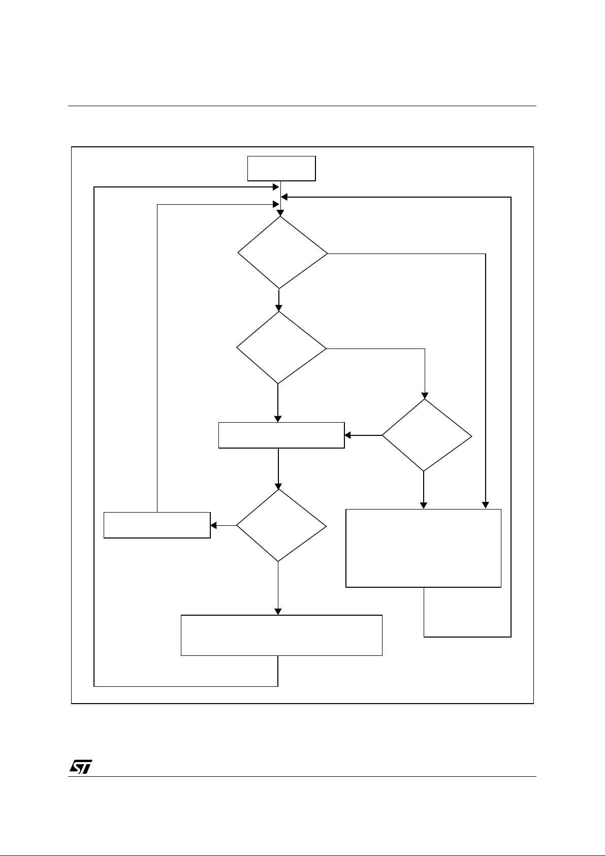
Figure 13. I nt errupt Processin g Fl owchart
FROM RESET
ST72774/ST727754/ST72734
EXECUTE INSTRUCTION
TRAP?
N
N
I BIT SET?
Y
FETCH NEXT INSTRUCTION
N
IRET?
Y
N
INTERRUPT?
Y
STACK PC, X, A, CC
SET I BIT
LOAD PC FROM INTERRUPT VECTOR
Y
RESTORE PC, X, A, CC FROM STACK
THIS CLEARS I BIT BY DEFAULT
VR01172D
23/144
ST72774/ST727754/ST72734
INTERRUPTS (Cont’d)
Table 6. Int errupt Mappin g
Source
Block
RESET Reset N/A N/A no FFFEh-FFFFh
TRAP Software N/A N/A no FFFCh-FFFDh
USB End Suspend Interrupt USBISTR ESUSP yes FFFAh-FFFBh
DDC/CI DDC/CI Interrupt
DDC1/2B DDC1/2B Interrupt DDCDCR EDF yes FFF6h-FFF7h
Port D bit 4 External Interrupt ITB
Port D bit 3 External Interrupt ITA ITALAT yes FFF2h-FFF3h
TIM
I2C
USB USB Interrupt USBISTR ** yes FFE6h-FFE7h
Description
Input Capture 1
Input Capture 2 ICF2
Output Compare 1 OCF1
Output Compare 2 OCF2
Timer Overflow TOF yes FFECh-FFEDh
I2C Peripheral Inter-
rupts
Register
Label
DDCSR1
DDCSR2
MISCR
TIMSR
I2CSR1
I2CSR2
Flag
** yes FFF8h-FFF9h
ITBLAT yes FFF4h-FFF5h
ICF1
** yes FFEAh-FFEBh
Maskable
by I-bit
yes FFF0h-FFF1h
yes FFEEh-FFEFh
Vector Address
Priority
Order
Highest
Priority
Lowest
Priority
** Many flags can cause an interrupt, see peripheral interrupt status register description.
24/144
3.4 POWER SAVI NG MO DE S
ST72774/ST727754/ST72734
3.4.1 WAIT Mode
This mode is a low power consumption mode. The
WFI instruction places the MCU in WAIT mode:
The internal clock remains active but all CPU
processing is stopped; however, all other
peripherals are still running.
Note: In WAIT mode, DMA accesses (DDC, USB)
are possible.
During WAIT mode, the I bit in the condition code
register is cleared to enable all interrupts, whi ch
causes the MCU to exit WAIT mode, causes the
corresponding interrupt vector to be fetched, th e
interrupt routine to be executed and normal
processing to resume. A reset causes the program
counter to fetch the reset vector and processing
starts as for a normal reset.
Table 5 gives a list of the different sections
affected by the low power modes. For detailed
information on a particular device, please refer to
the corresponding part.
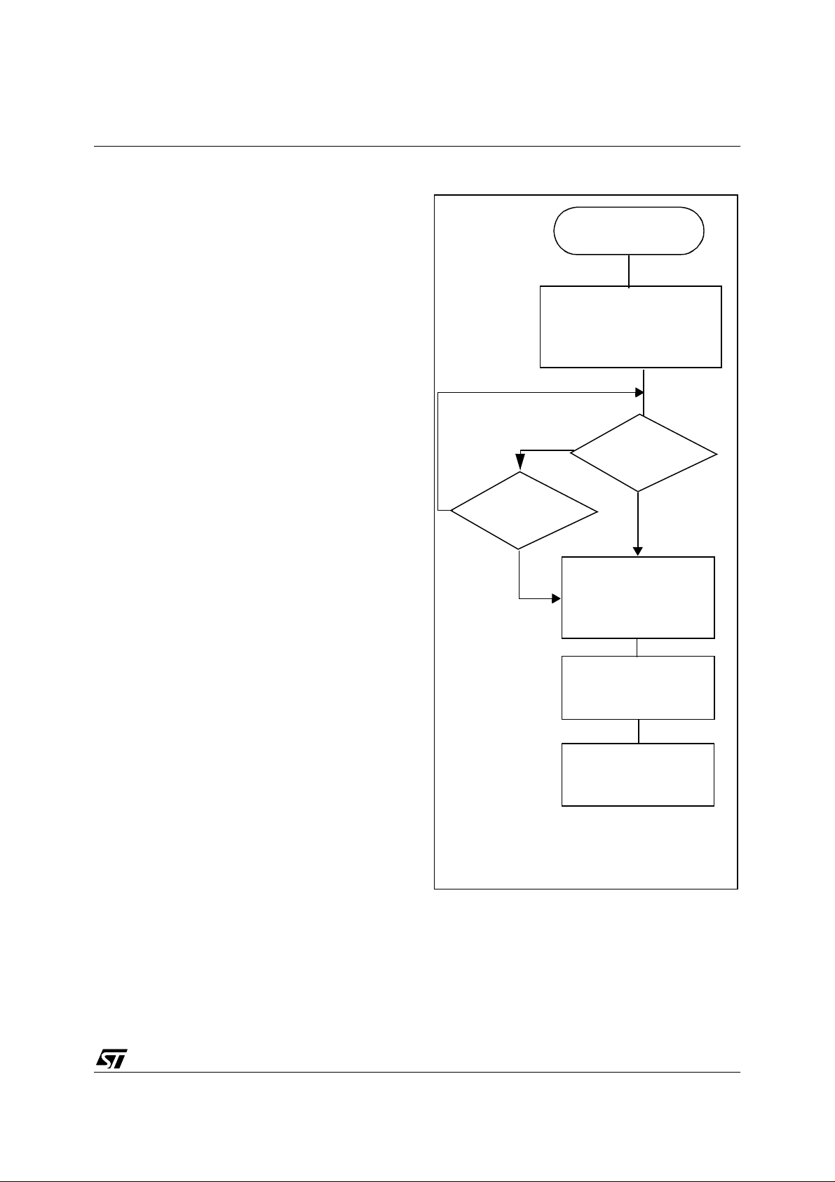
Figure 14. WAIT Flow Chart
WFI INSTRUCTION
OSCILLATOR
PERIPH. CLOCK
CPU CLOCK
I-BIT
N
N
INTERRUPT
Y
OSCILLATOR
PERIPH. CLOCK
CPU CLOCK
I-BIT
ON
ON
OFF
CLEARED
RESET
Y
ON
ON
ON
SET
3.4.2 HALT Mode
The HALT mode is the MCU lowest power
consumption mode. Meanwhile, the HALT mode
also stops the oscillator stage comple tely which is
the most critical condition in CRT monitors.
For this reason, the HALT mode has been disabled
and its associated HALT instruction is now
considered as illegal and will generate a reset.
IF RESET
4096 CPU CLOCK
CYCLES DELAY
FETCH RESET VECTOR
OR SERVICE INTERRUPT
Note: Before servicing an interrupt, the CC register is
pushed on the sta ck. T he I-Bit is s et d uring the inte rrupt routine and cleared when the CC register is
popped.
25/144

ST72774/ST727754/ST72734
3.5 MISCELLANEOUS REGISTER
MISCELLANEOUS REGISTER (MISCR)
Address: 0009h — R ea d/W rite
Reset Value: 0001 0000 (10h)
70
VSYNC
FLY_SYNHSYNC
SEL
FAST ITBLAT ITALAT ITBITE ITAITE
DIVEN
Bit 4= FAST
Fast Mode.
This bit is set and cleared by software. It is used to
select the external cloc k frequ ency . If th e exte rnal
clock frequency is 12 M Hz, this bit must be at 0,
else if the external frequency is 24 MHz, this bit
must be at 1.
Bit 7= VSYNCSEL
DDC1 VSYNC Selection.
This bit is set and cleared by software. It is used to
choose the VSYNC signal in DDC1 mode.
0: VSYNCI selected
1: VSYNCI2 selected
Note: VSYNCI 2 is only available for the DDC cell,
not for the SYNC processor cell.
Bit 6= FL Y _SY N
Flyback or Synchro Switch.
This bit is set and cleared by software. It is used to
choose the signals the Timing Measureme nt Unit
(TMU) will analyse.
0: horizontal and vertical synchro outputs analysis
1: horizontal and vertical Flyback inputs analysis
Bit 5= HS YNCDIVEN
HSYNCDIV Enable.
This bit is set and cleared by software. It is used to
enable the output of the HSYNCO output on PC0.
0: HSYNCDIV disabled
1:HSYNCDIV enabled
Bit 3= ITBLAT
Falling Edge Detector Latch.
This bit is set by hardware when a falling edge
occurs on pin ITB/PD4 in Port D. An interrupt is
generated if ITBITE=1and the I bit in the CC
register = 0. It is cleared by software.
0: No falling edge detected on ITB
1: Falling edge detected on ITB
Bit 2= ITALAT
Falling Edge Detector Latch.
This bit is set by hardware when a falling edge
occurs on pin ITA/PD3 in Port D. An interrupt is
generated if ITAITE=1and the I bit in the CC
register = 0. It is cleared by software.
0: No falling edge detected on ITA
1: Falling edge detected on ITA
Bit 1= ITBITE
ITB Interrupt Enable
.
This bit is set and cleared by software.
0: ITB interrupt disabled
1: ITB interrupt enabled
Bit 0= ITAITE
ITA Interrupt Enable
.
This bit is set and cleared by software.
26/144
0: ITA interrupt disabled
1: ITA interrupt enabled
4 ON-CHIP PERIPHERALS
4.1 I/O PORTS
ST72774/ST727754/ST72734
4.1.1 Introd uct i on
The I/O ports allow the transfer of data through
digital inputs and outputs, and, for specific pins,
the input of analog s ignals or the Input/Output of
alternate signals for on-chip peripherals (DDC,
TIMER...).
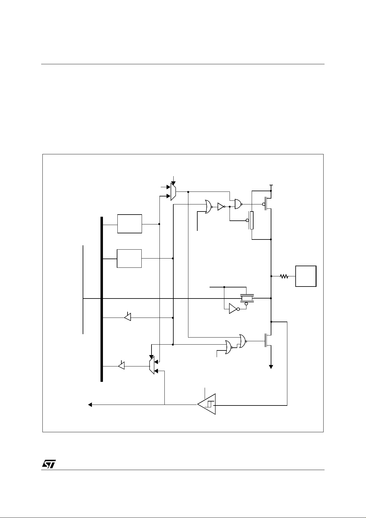
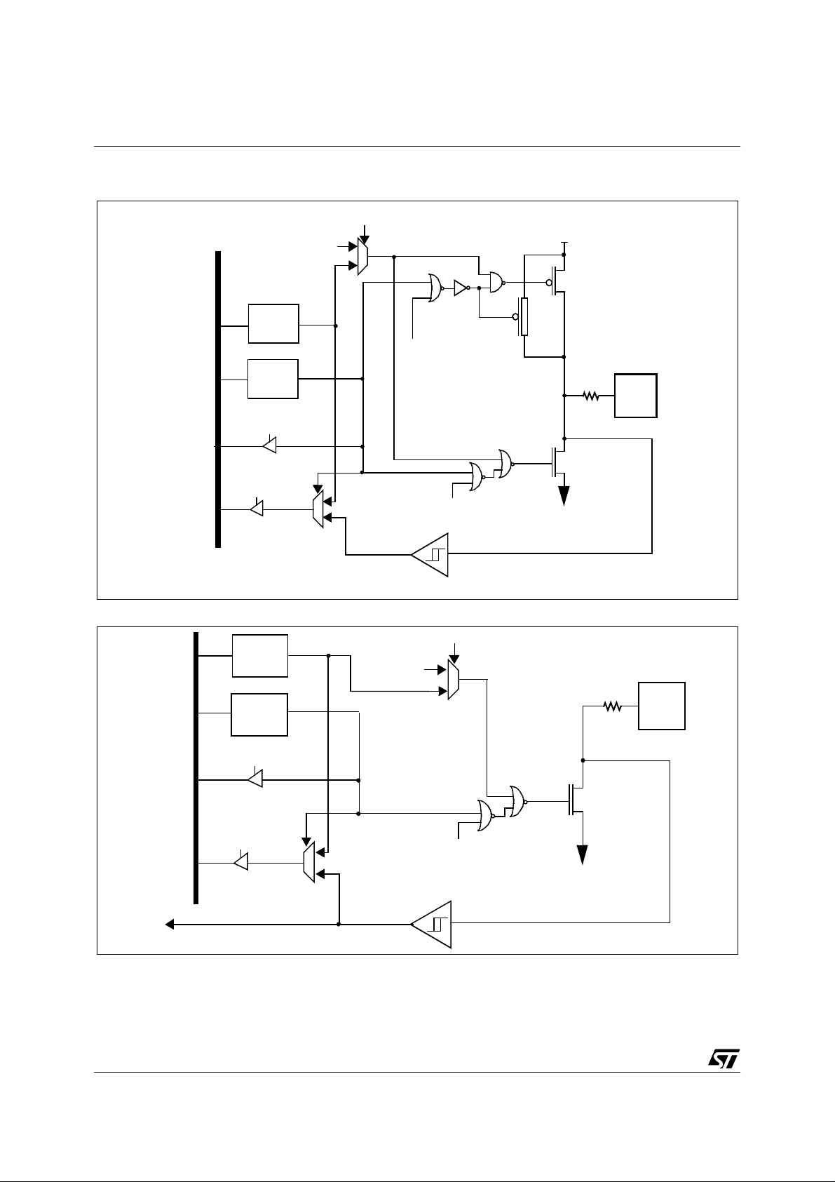
Figure 15. I/O Pin Typical Cir cuit
Alternate enable
Alternate
1
output
0
DR
latch
Data Bus
DDR
latch
Each pin can be programmed independently as
digital input or digital output. E ach pin can be an
analog input when an analog switch is connected
to the Analog to Digital Converter (ADC).
V
DD
P-BUFFER
(if required)
PULL-UP (if required)
Alternate enable
PAD
Analog Enable
(ADC)
Common Analog Rail
DDR SEL
Analog
Switch (if required)
N-BUFFER
DR SEL
1
Alternate Enable
0
Digital Enable
V
SS
Alternate Input
Note: This is the typical I/O pin configuration. For cost optimization, each port is customized with a specific configuration.
27/144
5

ST72774/ST727754/ST72734
I/O PORTS (Cont’d)
Table 7. I/O Pin Functions
DDR MODE
0 Input
1 Output
4.1.2 Common Functional Description
Each port pin of the I/O Ports can be individual ly
configured under software control as either i nput
or output.
Each bit of a Data Direction Register (DDR)
corresponds to an I/O pin of the associated p ort.
This corresponding bit must be set to configure its
associated pin as output and must be cleared to
configure its associated pin as input (Table 7, “. I/O
Pin Functions,” on page 28). The Data Direction
Registers can be read and written.
The typical I/O circuit is shown on Figure 15. Any
write to an I/O port updates the port data register
even if it is configured as input. Any read of an I/O
port returns either the data latched in the port data
register (pins configured as output) or the value of
the I/O pins (pins configured as input).
Remark: when an I/O pin does not exist inside an
I/O port, the returned value is a logic one (pin
configured as input).
At reset, all DDR registers are cleared, which
configures all port’s I/Os as inputs with or without
pull-ups (see Table 8 to Table 12 I/O Ports
Register Map). The Data Registers (DR) are also
initialized at reset.
4.1.2.1 Input mode
When DDR=0, the corresponding I/O is configured
in Input mode.
In this case, the output buffer is switched off, the
state of the I/O is readable through the Data
Register address, but the I/O state comes directly
from the CMOS Schmitt Trigger output and not
from the Data Register output.
4.1.2.2 Output mode
When DDR=1, the corresponding I/O is configured
in Output mode.
In this case, the output buffer is activated
according to the Data Register’s content.
A read operation is directly performed from the
Data Register output.
4.1.2.3 Analog input
Each I/O can be used as analog input by adding an
analog switch driven by the ADC.
The I/O must be configured in Input before using it
as analog input.
The CMOS Schmitt trigger is OFF and the analog
value directly input through an analog switch to the
Analog to Digital Converter, when the analog
channel is selected by the ADC.
4.1.2.4 Alternate mode
A signal coming from a on-chip peripheral can be
output on the I/O.
In this case, the I/O is automaticall y configured in
output mode.
This must be controlled directly by the peripheral
with a signal coming from the peripheral which
enables the alternate signal to be output.
A signal coming from an I/O can be inpu t in a onchip peripheral.
Before using an I/O as Alternate Input, it must be
configured in Input mode (DDR=0). So both
Alternate Input configuration and I/O Input
configuration are the same (with or without pullup). The signal to be input in the peripheral is taken
after the CMOS Schmitt trigger or TTL Schmitt
trigger for SYNC.
The I/O state is readable as in Input mode by
addressing the corresponding I/O Data Register.
28/144
ST72774/ST727754/ST72734
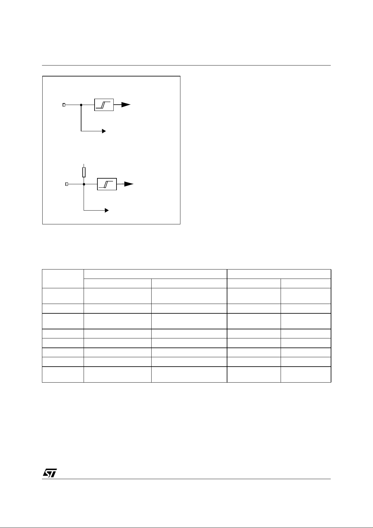
Figure 16. Input Structure for SYNC signals
TTL trigger
Pin
HSYNCI Input
VSYNCI Input
(no pull-up)
I/O logic (if existing)
V
DD
TTL trigg erpull-up
CSYNCI Input
Pin
HFBACK Input
VFBACK Input
I/O logic (if existing)
4.1.3 Port A
PA7 and PA[2:0] can be defined as Input lines
(with pull-up) or as Push-pull Outputs.
PA [6:3] can be defined as Input lines (without pullup) or as Output Open drain lines.
PA7 and PA[2:0] can be defined as Input lines
(with pull-up) or as Push-pull Outputs.
PA [6:3] can be defined as Input lines (without pullup) or as Output Open drain lines.
Table 8. Port A Description
PORT A
PA0 With pull-up push-pull OCMP1
PA1 With pull-up push-pull - PA2 With pull-up push-pull VSYNCI2
PA3 Without pull-up open-drain - -
PA4 Without pull-up open-drain - PA5 Without pull-up open-drain - PA6 Without pull-up open-drain - -
PA7 With pull-up push-pull BLANKOUT
*Reset State
Input* Output Signal Condition
I / O Alternate Function
OC1E =1
(CR2[TIMER])
VSYNCSEL=1
(MISCR)
BLKEN = 1
(ENR[SYNC])
29/144
ST72774/ST727754/ST72734
I/O PORTS (Cont’d)
Figure 17. PA0 to PA2, PA7
Alternate
output
Alternate enable
1
V
DD
DATA BUS
Figure 18. PA3 to PA6
DR
latch
DDR
latch
DDR SEL
DR SEL
DR
latch
DDR
latch
0
PULL-UP
OC1E
P-BUFFER
N-BUFFER
PAD
1
OC1E
V
SS
0
CMOS Schmitt Trigger
Alternate enable
Alternate
output
1
0
PAD
30/144
DATA BUS
Alternate input
DDR SEL
DR SEL
N-BUFFER
1
0
Alternate enable
CMOS Schmitt Trigger
V
SS
 Loading...