How it Works
Log In / Sign Up
Buy Points
How it Works
FAQ
Contact Us
Questions and Suggestions
Users
ST
Loading...
S
ST72361AR4
ST72361AR6
ST72361AR7
ST72361AR9
ST72361J4
ST72361J6
ST72361J7
ST72361J9
ST72361K4
ST72361K6
ST72361K7
ST72361K9
ST72511R
2
ST72512R
ST72521AR9
ST72521B
ST72521M9
ST72521R6
ST72521R9
ST72532R
2
ST72561
ST72561AR4
ST72561AR6
ST72561AR7
ST72561AR9
ST72561J4
ST72561J6
ST72561J7
ST72561J9
ST72561K4
ST72561K6
ST72561K7
ST72561K9
ST72561R4
ST72561R6
ST72561R7
ST72561R9
ST7260E1
ST7260E2
2
ST7260K1
ST7260K2
ST7261
ST72621J4
ST72621K4
ST72621L4
ST72622L2
ST72623F2
ST7263
ST7263B
ST72651AR6
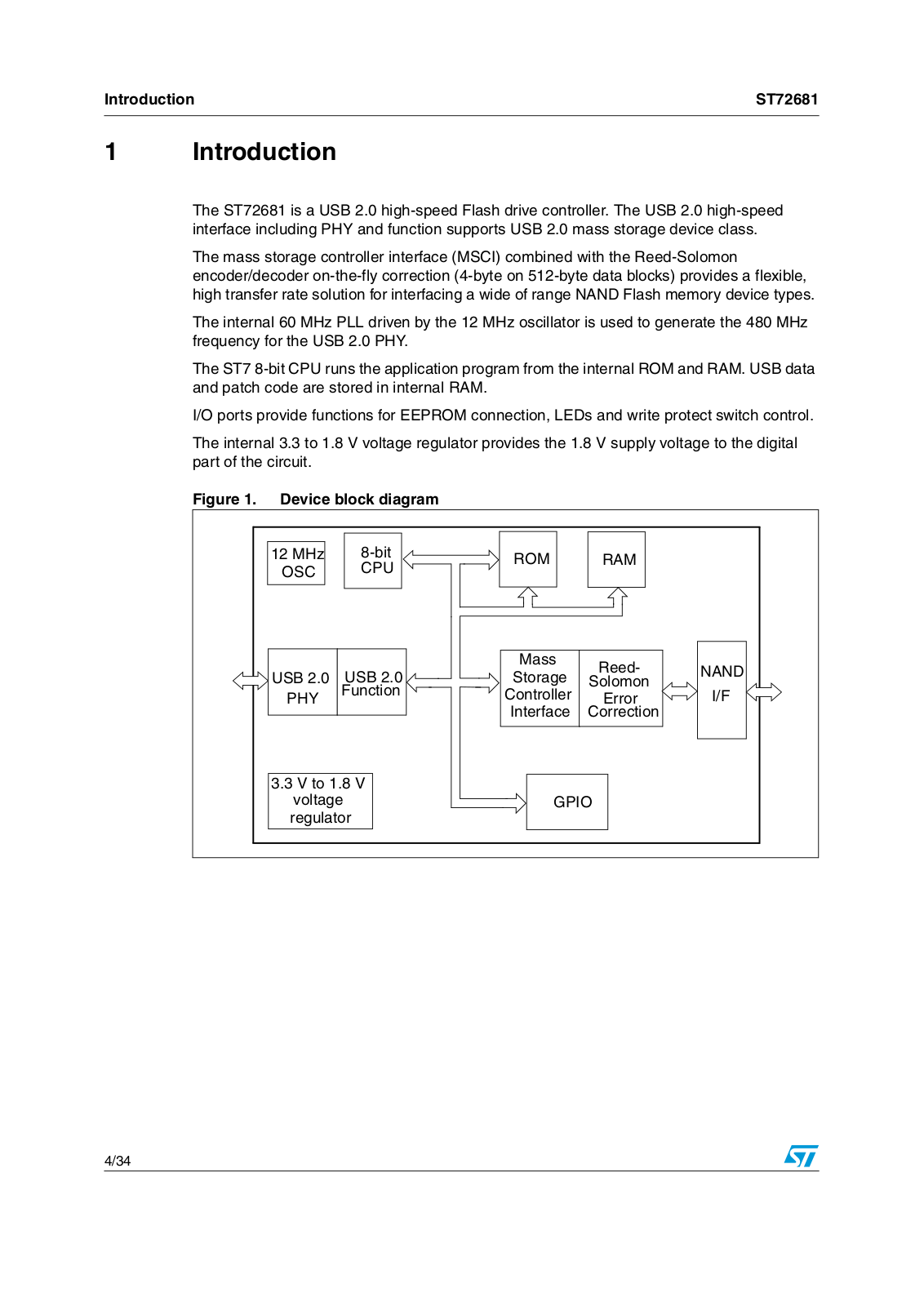
ST72681
ST72734
ST72754
ST72774
ST7291L
ST72C171
ST72E121
ST72E311
ST72E331
ST72F521
ST72F61
ST72F62
ST72F63B
ST72T121
ST72T311
ST72T331
ST75185C
ST7538Q
ST7540
2
ST7570
2
ST7580
2
ST7590
2
ST75 Series
ST763A
ST7920
ST7DALI
ST7DALIF2
ST7FLI49
ST7FLI49M
ST7FLIT1B
ST7FLITU0
ST7FLITUS
ST7FOXA0
ST7FOXF1
ST7FOXK1
ST7FOXK2
2
ST7GEME4
ST7LCRDIE6
ST7LCRE4U1
ST7LIT15BY0
ST7LITE02Y0
ST7LITE05Y0
ST7LITE09Y0
ST7LITE1
ST7LITE10B
ST7LITE15B
ST7LITE19B
ST7LITE2
ST7LITE30F2
ST7LITE35F2
Loading...
Loading...
Nothing found
ST72681
User Manual
34 pgs
601.92 Kb
0
Table of contents
Loading...
ST ST72681 User Manual
...
ST User Manual
Download
Specifications and Main Features
Frequently Asked Questions
User Manual
Download
Loading...
+
hidden pages
Unhide
You need points to download manuals.
1 point = 1 manual.
You can buy points or you can get point for every manual you upload.
Buy points
Upload your manuals
 Loading...