

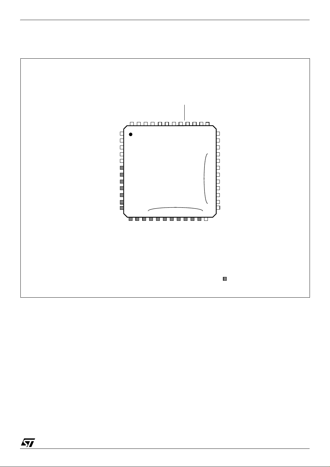
ST72651AR6
LQFP64 10x10
Low-power, full-speed USB 8-bit MCU with 32 KB Flash, 5 KB
RAM, Flash card interface, timer, PWM, ADC,
■ Memories
I2C, SPI
– Up to 32 KB of High Density Flash (HDFlash)
program memory with read/write protection
– For HDFlash devices, In-Application Pro-
gramming (IAP) via USB and In-Circuit programming (ICP)
– Up to 5 KB of RAM with up to 256 B stack
■ Clock, Reset and Supply Management
– PLL for generating 48 MHz USB clock using a
12 MHz crystal
– Low Voltage Reset (except on E suffix devic-
es)
– Dual supply management: analog voltage de-
tector on the USB power line to enable smart
power switching from USB power to battery
(on E suffix devices).
– Programmable Internal Voltage Regulator for
Memory cards (2.8V to 3.5V) supplying:
Flash Card I/O lines (voltage shifting)
Up to 50 mA for Flash card supply
– Clock-out capability
■ 47 programmable I/O lines
– 15 high sink I/Os (8mA@0.6V / 20mA@1.3V)
– 5 true open drain outputs
– 24 lines programmable as interrupt inputs
■ USB (Universal Serial Bus) Interface
– with DMA for full speed bulk applications com-
pliant with USB 12 Mbs specification (version
2.0 compliant)
– On-Chip 3.3V USB voltage regulator and
transceivers with software power-down
– 5 USB endpoints:
1 control endpoint
2 IN endpoints supporting interrupt and bulk
2 OUT endpoints supporting interrupt and
bulk
– Hardware conversion between USB bulk
packets and 512-byte blocks
■ Mass Storage Interface
– DTC (Data Transfer Coprocessor): Universal
Serial/Parallel communications interface, with
software plug-ins for current and future protocol standards:
Compact Flash - Multimedia Card -
Secure Digital Card - SmartMediaCard Sony Memory Stick - NAND Flash ATA Peripherals
■ 2 Timers
– Configurable Watchdog for system reliability
– 16-bit Timer with 2 output compare functions.
■ 2 Communication Interfaces
– SPI synchronous serial interface
2
C Single Master Interface up to 400 KHz
–I
■ D/A and A/D Peripherals
– PWM/BRM Generator (with 2 10-bit PWM/
BRM outputs)
– 8-bit A/D Converter (ADC) with 8 channels
■ Instruction Set
– 8-bit data manipulation
– 63 basic instructions
– 17 main addressing modes
– 8 x 8 unsigned multiply instruction
– True bit manipulation
■ Development Tools
– Full hardware/software development package
Device Summary
Features ST72651AR6
Program memory 32 Kbytes of Flash program memory
User RAM (stack) - bytes 5 Kbyte (256)
Peripherals USB, DTC, Timer, ADC, SPI, I
Operating Supply 4.0 to 5.5 V (for USB) Dual 3.0 to 5.5 V or 4.0 to 5.5 V (for USB)
Package LQFP64 (10 x10)
Operating Temperature 0 to +70 °C
2
C, PWM, WDT
June 2009 1/161
Doc ID 7215 Rev 4
1

Table of Contents
1 INTRODUCTION . . . . . . . . . . . . . . . . . . . . . . . . . . . . . . . . . . . . . . . . . . . . . . . . . . . . . . . . . . . . . . 4
2 PIN DESCRIPTION . . . . . . . . . . . . . . . . . . . . . . . . . . . . . . . . . . . . . . . . . . . . . . . . . . . . . . . . . . . . 7
3 REGISTER & MEMORY MAP . . . . . . . . . . . . . . . . . . . . . . . . . . . . . . . . . . . . . . . . . . . . . . . . . . . 16
4 FLASH PROGRAM MEMORY . . . . . . . . . . . . . . . . . . . . . . . . . . . . . . . . . . . . . . . . . . . . . . . . . . 20
4.1 INTRODUCTION . . . . . . . . . . . . . . . . . . . . . . . . . . . . . . . . . . . . . . . . . . . . . . . . . . . . . . . . 20
4.2 MAIN FEATURES . . . . . . . . . . . . . . . . . . . . . . . . . . . . . . . . . . . . . . . . . . . . . . . . . . . . . . . 20
4.3 STRUCTURE . . . . . . . . . . . . . . . . . . . . . . . . . . . . . . . . . . . . . . . . . . . . . . . . . . . . . . . . . . . 20
4.4 READ-OUT PROTECTION . . . . . . . . . . . . . . . . . . . . . . . . . . . . . . . . . . . . . . . . . . . . . . . . 20
4.5 ICC INTERFACE . . . . . . . . . . . . . . . . . . . . . . . . . . . . . . . . . . . . . . . . . . . . . . . . . . . . . . . . 21
4.6 ICP (IN-CIRCUIT PROGRAMMING) . . . . . . . . . . . . . . . . . . . . . . . . . . . . . . . . . . . . . . . . . 22
4.7 IAP (IN-APPLICATION PROGRAMMING) . . . . . . . . . . . . . . . . . . . . . . . . . . . . . . . . . . . . . 22
4.8 RELATED DOCUMENTATION . . . . . . . . . . . . . . . . . . . . . . . . . . . . . . . . . . . . . . . . . . . . . 22
4.9 REGISTER DESCRIPTION . . . . . . . . . . . . . . . . . . . . . . . . . . . . . . . . . . . . . . . . . . . . . . . . 22
5 CENTRAL PROCESSING UNIT . . . . . . . . . . . . . . . . . . . . . . . . . . . . . . . . . . . . . . . . . . . . . . . . . 23
5.1 INTRODUCTION . . . . . . . . . . . . . . . . . . . . . . . . . . . . . . . . . . . . . . . . . . . . . . . . . . . . . . . . 23
5.2 MAIN FEATURES . . . . . . . . . . . . . . . . . . . . . . . . . . . . . . . . . . . . . . . . . . . . . . . . . . . . . . . 23
5.3 CPU REGISTERS . . . . . . . . . . . . . . . . . . . . . . . . . . . . . . . . . . . . . . . . . . . . . . . . . . . . . . . 23
6 SUPPLY, RESET AND CLOCK MANAGEMENT . . . . . . . . . . . . . . . . . . . . . . . . . . . . . . . . . . . . 26
6.1 CLOCK SYSTEM . . . . . . . . . . . . . . . . . . . . . . . . . . . . . . . . . . . . . . . . . . . . . . . . . . . . . . . . 26
6.2 RESET SEQUENCE MANAGER (RSM) . . . . . . . . . . . . . . . . . . . . . . . . . . . . . . . . . . . . . . 27
6.3 LOW VOLTAGE DETECTOR (LVD) . . . . . . . . . . . . . . . . . . . . . . . . . . . . . . . . . . . . . . . . . 30
6.4 POWER SUPPLY MANAGEMENT . . . . . . . . . . . . . . . . . . . . . . . . . . . . . . . . . . . . . . . . . . 31
7 INTERRUPTS . . . . . . . . . . . . . . . . . . . . . . . . . . . . . . . . . . . . . . . . . . . . . . . . . . . . . . . . . . . . . . . 37
7.1 INTRODUCTION . . . . . . . . . . . . . . . . . . . . . . . . . . . . . . . . . . . . . . . . . . . . . . . . . . . . . . . . 37
7.2 MASKING AND PROCESSING FLOW . . . . . . . . . . . . . . . . . . . . . . . . . . . . . . . . . . . . . . . 37
7.3 INTERRUPTS AND LOW POWER MODES . . . . . . . . . . . . . . . . . . . . . . . . . . . . . . . . . . . 39
7.4 CONCURRENT & NESTED MANAGEMENT . . . . . . . . . . . . . . . . . . . . . . . . . . . . . . . . . . 39
7.5 INTERRUPT REGISTER DESCRIPTION . . . . . . . . . . . . . . . . . . . . . . . . . . . . . . . . . . . . . 40
8 POWER SAVING MODES . . . . . . . . . . . . . . . . . . . . . . . . . . . . . . . . . . . . . . . . . . . . . . . . . . . . . 43
8.1 INTRODUCTION . . . . . . . . . . . . . . . . . . . . . . . . . . . . . . . . . . . . . . . . . . . . . . . . . . . . . . . . 43
8.2 WAIT MODE . . . . . . . . . . . . . . . . . . . . . . . . . . . . . . . . . . . . . . . . . . . . . . . . . . . . . . . . . . . 43
-
8.3 HALT MODE . . . . . . . . . . . . . . . . . . . . . . . . . . . . . . . . . . . . . . . . . . . . . . . . . . . . . . . . . . . 44
9 I/O PORTS . . . . . . . . . . . . . . . . . . . . . . . . . . . . . . . . . . . . . . . . . . . . . . . . . . . . . . . . . . . . . . . . . . 45
9.1 INTRODUCTION . . . . . . . . . . . . . . . . . . . . . . . . . . . . . . . . . . . . . . . . . . . . . . . . . . . . . . . . 45
9.2 FUNCTIONAL DESCRIPTION . . . . . . . . . . . . . . . . . . . . . . . . . . . . . . . . . . . . . . . . . . . . . . 45
9.3 I/O PORT IMPLEMENTATION . . . . . . . . . . . . . . . . . . . . . . . . . . . . . . . . . . . . . . . . . . . . . . 49
9.4 REGISTER DESCRIPTION . . . . . . . . . . . . . . . . . . . . . . . . . . . . . . . . . . . . . . . . . . . . . . . . 50
10 MISCELLANEOUS REGISTERS . . . . . . . . . . . . . . . . . . . . . . . . . . . . . . . . . . . . . . . . . . . . . . . 52
11 ON-CHIP PERIPHERALS . . . . . . . . . . . . . . . . . . . . . . . . . . . . . . . . . . . . . . . . . . . . . . . . . . . . . 54
11.1 WATCHDOG TIMER (WDG) . . . . . . . . . . . . . . . . . . . . . . . . . . . . . . . . . . . . . . . . . . . . . . . 54
11.2 DATA TRANSFER COPROCESSOR (DTC) . . . . . . . . . . . . . . . . . . . . . . . . . . . . . . . . . . . 57
11.3 USB INTERFACE (USB) . . . . . . . . . . . . . . . . . . . . . . . . . . . . . . . . . . . . . . . . . . . . . . . . . . 61
2/161
1
Doc ID 7215 Rev 4

Table of Contents
11.4 16-BIT TIMER . . . . . . . . . . . . . . . . . . . . . . . . . . . . . . . . . . . . . . . . . . . . . . . . . . . . . . . . . . 76
11.5 PWM/BRM GENERATOR (DAC) . . . . . . . . . . . . . . . . . . . . . . . . . . . . . . . . . . . . . . . . . . . . 88
11.6 SERIAL PERIPHERAL INTERFACE (SPI) . . . . . . . . . . . . . . . . . . . . . . . . . . . . . . . . . . . . 94
11.7 I²C SINGLE MASTER BUS INTERFACE (I2C) . . . . . . . . . . . . . . . . . . . . . . . . . . . . . . . . 105
11.8 8-BIT A/D CONVERTER (ADC) . . . . . . . . . . . . . . . . . . . . . . . . . . . . . . . . . . . . . . . . . . . . 114
12 INSTRUCTION SET . . . . . . . . . . . . . . . . . . . . . . . . . . . . . . . . . . . . . . . . . . . . . . . . . . . . . . . . 118
12.1 CPU ADDRESSING MODES . . . . . . . . . . . . . . . . . . . . . . . . . . . . . . . . . . . . . . . . . . . . . . 118
12.2 INSTRUCTION GROUPS . . . . . . . . . . . . . . . . . . . . . . . . . . . . . . . . . . . . . . . . . . . . . . . . 121
13 ELECTRICAL CHARACTERISTICS . . . . . . . . . . . . . . . . . . . . . . . . . . . . . . . . . . . . . . . . . . . . 124
13.1 PARAMETER CONDITIONS . . . . . . . . . . . . . . . . . . . . . . . . . . . . . . . . . . . . . . . . . . . . . . 124
13.2 ABSOLUTE MAXIMUM RATINGS . . . . . . . . . . . . . . . . . . . . . . . . . . . . . . . . . . . . . . . . . . 125
13.3 OPERATING CONDITIONS . . . . . . . . . . . . . . . . . . . . . . . . . . . . . . . . . . . . . . . . . . . . . . . 126
13.4 SUPPLY CURRENT CHARACTERISTICS . . . . . . . . . . . . . . . . . . . . . . . . . . . . . . . . . . . 128
13.5 CLOCK AND TIMING CHARACTERISTICS . . . . . . . . . . . . . . . . . . . . . . . . . . . . . . . . . . 131
13.6 MEMORY CHARACTERISTICS . . . . . . . . . . . . . . . . . . . . . . . . . . . . . . . . . . . . . . . . . . . 132
13.7 EMC CHARACTERISTICS . . . . . . . . . . . . . . . . . . . . . . . . . . . . . . . . . . . . . . . . . . . . . . . 133
13.8 I/O PORT PIN CHARACTERISTICS . . . . . . . . . . . . . . . . . . . . . . . . . . . . . . . . . . . . . . . . 135
13.9 CONTROL PIN CHARACTERISTICS . . . . . . . . . . . . . . . . . . . . . . . . . . . . . . . . . . . . . . . 139
13.10TIMER PERIPHERAL CHARACTERISTICS . . . . . . . . . . . . . . . . . . . . . . . . . . . . . . . . . 142
13.11COMMUNICATION INTERFACE CHARACTERISTICS . . . . . . . . . . . . . . . . . . . . . . . . 143
13.128-BIT ADC CHARACTERISTICS . . . . . . . . . . . . . . . . . . . . . . . . . . . . . . . . . . . . . . . . . . 148
14 PACKAGE CHARACTERISTICS . . . . . . . . . . . . . . . . . . . . . . . . . . . . . . . . . . . . . . . . . . . . . . 150
14.1 PACKAGE MECHANICAL DATA . . . . . . . . . . . . . . . . . . . . . . . . . . . . . . . . . . . . . . . . . . . 150
14.2 THERMAL CHARACTERISTICS . . . . . . . . . . . . . . . . . . . . . . . . . . . . . . . . . . . . . . . . . . 152
15 DEVICE CONFIGURATION AND ORDERING INFORMATION . . . . . . . . . . . . . . . . . . . . . . . 153
15.1 OPTION BYTE . . . . . . . . . . . . . . . . . . . . . . . . . . . . . . . . . . . . . . . . . . . . . . . . . . . . . . . . . 153
15.2 DEVICE ORDERING INFORMATION . . . . . . . . . . . . . . . . . . . . . . . . . . . . . . . . . . . . . . . 154
15.3 DEVELOPMENT TOOLS . . . . . . . . . . . . . . . . . . . . . . . . . . . . . . . . . . . . . . . . . . . . . . . . . 155
15.4 ST7 APPLICATION NOTES . . . . . . . . . . . . . . . . . . . . . . . . . . . . . . . . . . . . . . . . . . . . . . 156
16 IMPORTANT NOTES . . . . . . . . . . . . . . . . . . . . . . . . . . . . . . . . . . . . . . . . . . . . . . . . . . . . . . . 159
16.1 SPI MULTIMASTER MODE . . . . . . . . . . . . . . . . . . . . . . . . . . . . . . . . . . . . . . . . . . . . . . . 159
16.2 IN-CIRCUIT PROGRAMMING OF DEVICES PREVIOUSLY PROGRAMMED WITH HARD-
WARE WATCHDOG OPTION . . . . . . . . . . . . . . . . . . . . . . . . . . . . . . . . . . . . . . . . . . . . . 159
16.3 UNEXPECTED RESET FETCH . . . . . . . . . . . . . . . . . . . . . . . . . . . . . . . . . . . . . . . . . . . . 159
16.4 I2C MULTIMASTER . . . . . . . . . . . . . . . . . . . . . . . . . . . . . . . . . . . . . . . . . . . . . . . . . . . . . 159
17 SUMMARY OF CHANGES . . . . . . . . . . . . . . . . . . . . . . . . . . . . . . . . . . . . . . . . . . . . . . . . . . . 160
Doc ID 7215 Rev 4
3/161
1
ST72651AR6
512-byte RAM
Buffer
512-byte RAM
Buffer
DATA
COPROCESSOR
DATA TRANSFER
BUFFER
LEVEL
SHIFTERS
MASS
DEVICE
USB
SIE
ST7 CORE
STORAGE
TRANSFER
(DTC)
ARBITRATION
USB DATA
TRANSFER
BUFFER ACCESS
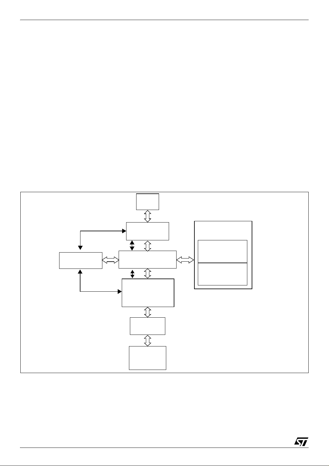
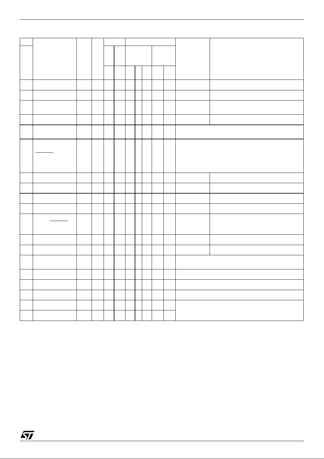
1 INTRODUCTION
The ST7265x MCU supports volume data exchange with a host (computer or kiosk) via a full
speed USB interface. The MCU is capable of handling various transfer protocols, with a particular
emphasis on mass storage applications.
ST7265x is compliant with the USB Mass Storage
Class specifications, and supports related protocols such as BOT (Bulk Only Transfer) and CBI
(Control, Bulk, Interrupt).
It is based on the ST7 standard 8-bit core, with
specific peripherals for managing USB full speed
data transfer between the host and most types of
FLASH media card:
– A full speed USB interface with Serial Interface
Engine, and on-chip 3.3V regulator and transceivers.
– A dedicated 24 MHz Data Buffer Manager state
machine for handling 512-byte data blocks (this
Figure 1. USB Data Transfer Block Diagram
size corresponds to a sector both on computers
and FLASH media cards).
– A Data Transfer Coprocessor (DTC), able to
handle fast data transfer with external devices.
This DTC also computes the CRC or ECC required to handle Mass storage media.
– An Arbitration block gives the ST7 core priority
over the USB and DTC when accessing the Data
Buffer. In USB mode, the USB interface is serviced before the DTC.
– A FLASH Supply Block able to provide program-
mable supply voltage and I/O electrical levels to
the FLASH media.
Related Documentation
AN1475: Developing an ST7265x Mass Storage
Application
4/161
1
Doc ID 7215 Rev 4
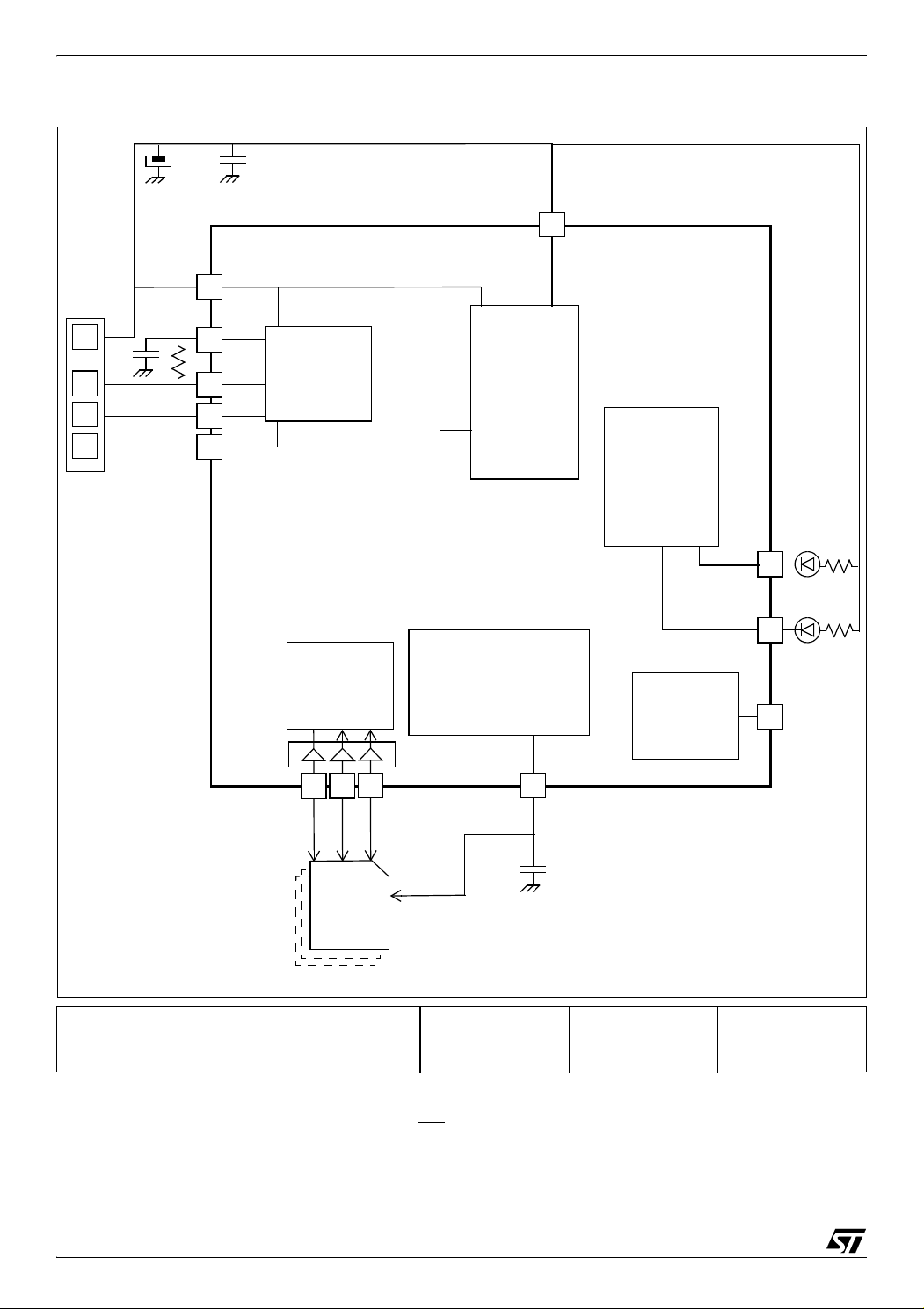
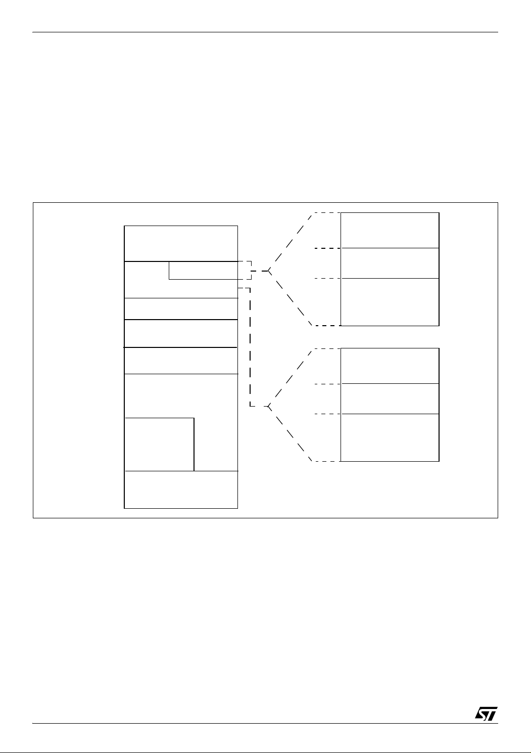
INTRODUCTION (Cont’d)
512-byte RAM
Buffer
512-byte RAM
Buffer
DATA
COPROCESSOR
DATA TRANSFER
BUFFER
LEVEL SHIFTERS
MASS
DEVICE
ST7 CORE
STORAGE
TRANSFER
(DTC)
ARBITRATION
BUFFER ACCESS
DIGITAL
AUDIO DEVICE
I2C
In addition to the peripherals for USB full speed
data transfer, the ST7265x includes all the necessary features for stand-alone applications with
FLASH mass storage.
– Low voltage reset ensuring proper power-on or
power-off of the device (not on all products)
– Digital Watchdog
– 16-bit Timer with 2 output compare functions (not
on all products - see device summary).
– Serial Peripheral interface (not on all products -
see device summary)
2
– Fast I
C Single Master interface (not on all prod-
ucts - see device summary)
– 8-bit Analog-to-Digital converter (ADC) with 8
multiplexed analog inputs (not on all products see device summary)
The ST72F65x are the Flash versions of the
ST7265x in a LQFP64 package.
– Two 10-bit PWM outputs (not on all products -
see device summary)
Figure 2. Digital Audio Player Application Example in Play Mode
ST72651AR6
Doc ID 7215 Rev 4
5/161
1
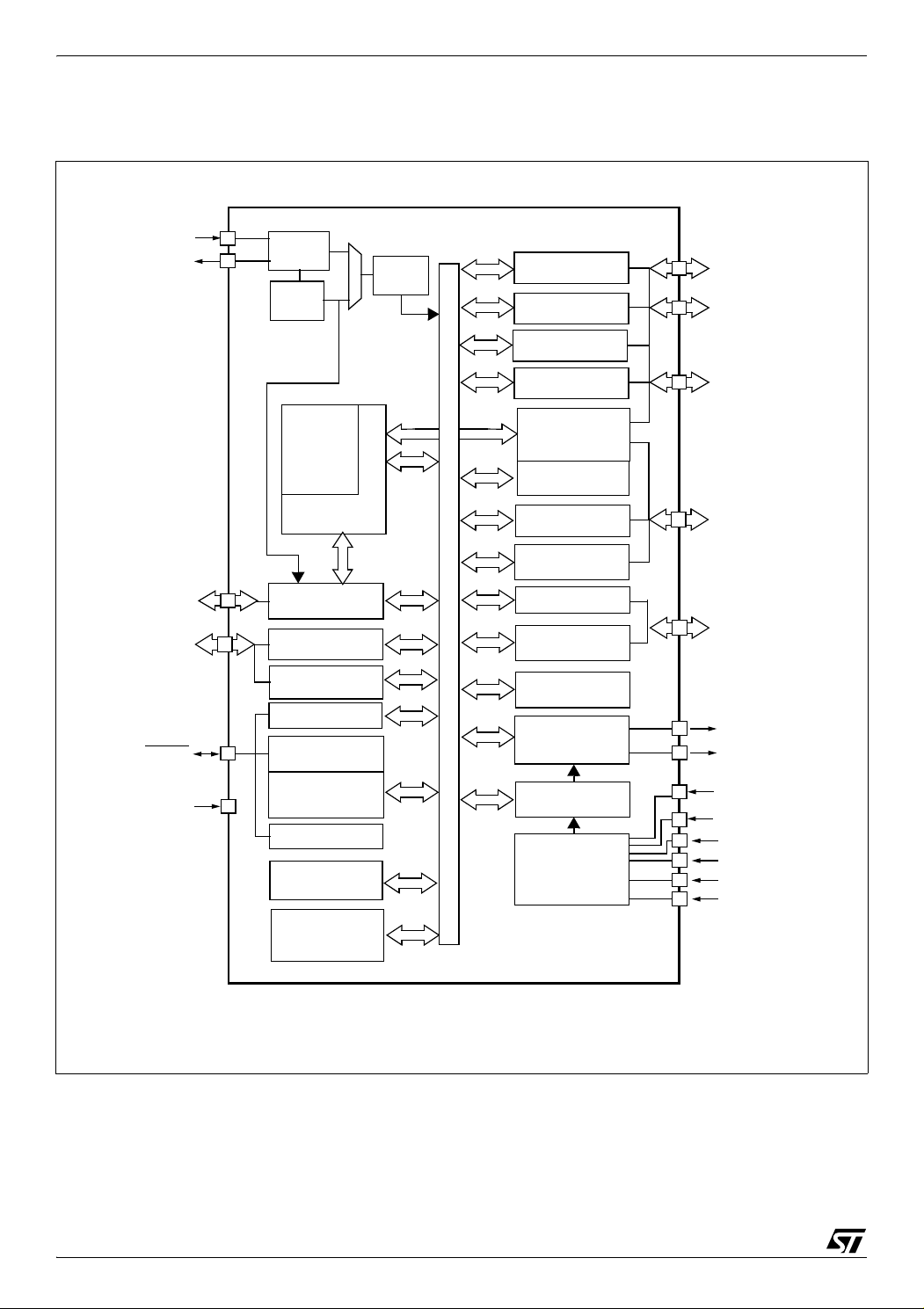
ST72651AR6
8-BIT CORE
ALU
ADDRESS AND DATA BUS
OSCIN
OSCOUT
RESET
DATA
PD[7:0]
(8 bits)
12MHz
f
CPU
CONTROL
RAM
(0.5/5 KBytes)
PROGRAM
(16/32 Kbytes)
MEMORY
16-BIT TIMER*
LVD*
WATCHDOG
V
DDA
V
PP
USBDP
USBDM
USBVCC
* not available on all products (refer to Table 1: Device Summary)
TRANSFER
COPROCESSOR
PORT C
PORT E
PORT D
PE[7:0]
(8 bits)
PC[7:0]
(8 bits)
PB[7:0]
(8 bits)
PA[7:0]
(8 bits)
PORT F
PF[6:0]
(7 bits)
8-BIT ADC*
I2C*
FLASH SUPPLY
V
DDF
V
SSA
POWER SUPPLY
DUAL SUPPLY
USBVSS
MANAGER *
BLOCK
48MHz
PLL
CLOCK
DIVIDER
OSC
USB
V
SSF
USBVDD
V
SS1, VSS2
V
DD1,VDD2
PWM*
PORT B
PORT A
DATA
TRANSFER
BUFFER
(1280 bytes)
DTC S/W RAM
(256 Bytes)
REGULATOR
ARBITRATION
SPI *
INTRODUCTION (Cont’d)
Figure 3. ST7265x Block Diagram
6/161
1
Doc ID 7215 Rev 4
2 PIN DESCRIPTION
44 43 42 41 40 39 38 37
36
35
34
33
32
31
30
29
28
27
26
25
24
23
12
13 14 15 16 17 18 19 20 21 22
1
2
3
4
5
6
7
8
9
10
11
48 47 46 45
V
DDAVDD2
PF6 (HS) / ICCDATA
PF5 (HS)/ICCCLK
RESET
V
PP/
ICCSEL
PE4
OSCOUT
OSCIN
V
SS2VSSA
USBV
DD
V
DDF
V
SSF
DTC/PB0
DTC/PB1
DTC/PB3
USBV
SS
USBDM
USBDP
USBVCC
DTC / PA0
DTC / PA1
DTC / PA2
DTC / PA3
DTC / PA4
DTC / PA5
DTC / PA6
DTC / PA7
DTC/PB5
DTC/PB6
DTC/PB7
PE2 (HS) / DTC
PE1 (HS) / DTC
PE0 (HS) / DTC
PD7
V
SS1
V
DD1
PD0
PD1
PD2
PD3
PD5
PD6
PD4
PE3/DTC
DTC/PB2
DTC/PB4
(HS) high sink capability
eixassociated external interrupt vector
I/O pin supplied by V
DDF
/ V
SSF
ei1
ei0
Figure 4. 48-Pin LQFP Package Pinout
ST72651AR6
Doc ID 7215 Rev 4
7/161
1
ST72651AR6
DTC / PA2
DTC / PA3
DTC / PA4
DTC / PA5
DTC / PA6
DTC / PA7
SS
/ MCO / (HS) PC0
MISO / DTC / (HS) PC1
MOSI / DTC / (HS) PC2
SCK / DTC / (HS) PC3
V
DD1
V
SS1
DTC / PB6
DTC / PB7
DTC / PA0
DTC / PA1
64 63 62 61 60 59 58 57 56 55 54 53 52 51 50 49
48
47
46
45
44
43
42
41
40
39
38
37
36
35
34
33
17 18 19 20 21 22 23 24 29 30 31 3225 26 27 28
1
2
3
4
5
6
7
8
9
10
11
12
13
14
15
16
ei1
ei0
USBV
DD
V
DDF
V
SSF
DTC / PE5 (HS)
DTC / PE6 (HS)
DTC / PE7 (HS)
DTC / PB0
DTC / PB1
DTC / PB2
DTC / PB3
DTC / PB4
DTC / PB5
USBV
SS
USBDM
USBDP
USBVCC
PD7 / AIN3
PD6 / AIN2
PD5/OCMP2
PD4/OCMP1
PD3
PD2
PD1
PD0
PC7
PC6
PC5
PC4
PE3 / PWM0 / AIN7 / DTC
PE2 (HS) / AIN6 / DTC
PE1 (HS) / AIN5 / DTC
PE0 (HS) / AIN4 / DTC
V
DDAVDD2
PF6 (HS)/ICCDATA
PF5 (HS)/ICCCLK
PF4 (HS) / USBEN
PF3 / AIN1
PF2 / AIN0
PF1 (HS) / SDA
PF0 (HS) / SCL
RESET
V
PP
/ICCSEL
PE4 / PWM1
OSCOUT
OSCIN
V
SS2VSSA
(HS) high sink capability
ei
x
associated external interrupt vector
I/O pin supplied by V
DDF
/ V
SSF
ei2
ei2
PIN DESCRIPTION (Cont’d)
Figure 5. 64-Pin LQFP Package Pinout
8/161
1
Doc ID 7215 Rev 4
PIN DESCRIPTION (Cont’d)
Legend / Abbreviations:
Type: I = input, O = output, S = supply
V
powered: I/O powered by the alternate sup-
DDF
ply rail, supplied by V
In/Output level: C
T
DDF
and V
SSF
.
= CMOS 0.3VDD/0.7VDD with
input trigger
Output level: HS = High Sink (on N-buffer only)
Port and control configuration:
– Input:float = floating, wpu = weak pull-up, int = in-
terrupt
– Output: OD = open drain, T = true open drain, PP
= push-pull, OP = pull-up enabled by option byte.
Refer to “I/O PORTS” on page 45 for more details
on the software configuration of the I/O ports.
The RESET configuration of each pin is shown in
bold.
Table 1. Device Pin Description
Pin
Pin Name
LQFP64
1USBV
2 USBDM I/O USB bidirectional data (data -)
3 USBDP I/O USB bidirectional data (data +)
4 USBVCC O
5USBV
6V
7V
8 PE5/DTC I/O X C
9 PE6/DTC I/O X C
10 PE7/DTC I/O X C
11 PB0/DTC I/O X CT X X Port B0 DTC
12 PB1/DTC I/O X CT X X Port B1 DTC
13 PB2/DTC I/O X CT X X Port B2 DTC
14 PB3/
SS
DD
DDF
SSF
DTC I/O X CT X X Port B3 DTC
Type
S USB Digital ground
S
SX
SX
Level Port / Control
Input Output
Output
int
wpu
float
2)
HS X
HS X X X Port E6
HS X X X Port E7
X2)XPort E5
Powered
DDF
V
Input
T
T
T
OD
Main
Function
(after reset)
PP
USB power supply, output by the on-chip USB 3.3V
linear regulator.
Note: An external decoupling capacitor (typ. 100nF,
min 47nF) must be connected between this pin and
SS
.
DTC I/O with serial capability
(MMC_CMD)
DTC I/O with serial capability
(MMC_DAT)
DTC I/O with serial capability
(MMC_CLK)
USBV
USB Power supply voltage (4V - 5.5V) also used by
the regulator and PLL
Note: External decoupling capacitors (typ.
4.7µF+100nF, min 2.2µF+100nFmust be connected
between this pin and USBV
Power Line for alternate supply rail. Can be used as
input (with external supply) or output (when using the
on-chip voltage regulator). Note: An external decoupling capacitor (min. 20nF) must be connected to this
pin to stabilize the regulator.
Ground Line for alternate supply rail. Can be used as
input (with external supply) or output (when using the
on-chip voltage regulator)
Alternate Function
ST72651AR6
.
SS
Doc ID 7215 Rev 4
9/161
1
ST72651AR6
Pin
Pin Name
LQFP64
15 PB4/DTC I/O X CT X X Port B4 DTC
16 PB5/DTC I/O X CT X X Port B5 DTC
17 PB6/DTC I/O X CT X X Port B6 DTC
18 PB7/DTC I/O X CT X X Port B7 DTC
19 PA0/DTC I/O X CT X
20 PA1/DTC I/O X CT X X X Port A1 DTC
21 PA2/DTC I/O X CT X X X Port A2 DTC
22 PA3/DTC I/O X CT X X X Port A3 DTC
23 PA4/DTC I/O X CT X X X Port A4 DTC
24 PA5/DTC I/O X CT X X X Port A5 DTC
25 PA6/DTC I/O X CT X X X Port A6 DTC
26 PA7/DTC I/O X CT X X X Port A7 DTC
27 PC0/MCO/SS
28 PC1/DTC/MIS0 I/O X CTHS X X Port C1
29 PC2/DTC/MOSI I/O X CTHS X X Port C2
30 PC3/DTC/SCK I/O X CTHS X X Port C3
31 V
DD1
32 V
SS1
33 PC4/DTC I/O C
34 PC5/DTC I/O C
35 PC6/DTC I/O C
36 PC7/DTC I/O C
37 PD0 I/O CT X
38 PD1 I/O CT X X X Port D1
39 PD2 I/O CT X X X Port D2
40 PD3 I/O CT X X X Port D3
41 PD4/OCMP1 I/O CT X X X Port D4 Timer Output Compare 1
42 PD5/OCMP2 I/O CT X X X Port D5 Timer Output Compare 2
43 PD6/AIN2 I/O CT X X X Port D6 Analog Input 2
44 PD7/AIN3 I/O CT X X X Port D7 Analog Input 3
45 PE0/DTC/AIN4 I/O CT HS X X X Port E0 Analog Input 4
Type
I/O X CT HS X
S Power supply voltage (3V - 5.5V)
S Digital ground
Level Port / Control
Input Output
Output
wpu
float
ei0
ei2
X
X X Port C5 DTC
ei2
X X Port C6 DTC
X X Port C7 DTC
ei1
Powered
DDF
V
Input
T
T
T
T
Main
Function
(after reset)
int
PP
OD
X X Port A0 DTC
XPort C0
X Port C4 DTC
XXPort D0
Alternate Function
Main Clock Output / SPI Slave
1)
Select
DTC I/O with serial capability (DA-
TARQ) / SPI Master In Slave Out
DTC I/O with serial capability (SDAT) /
SPI Master Out Slave In
DTC I/O with serial capability (SCLK) /
SPI Serial Clock
1)
1)
1)
1)
/ DTC
1)
1)
1)
1)
10/161
1
Doc ID 7215 Rev 4
ST72651AR6
Pin
Pin Name
Type
LQFP64
Level Port / Control
Input Output
Input
Powered
DDF
V
Output
float
wpu
int
OD
Main
Function
(after reset)
PP
Alternate Function
46 PE1/DTC/AIN5 I/O CTHS X X X Port E1 Analog Input 5
47 PE2/DTC/AIN6 I/O C
PE3/AIN7/DTC/
48
PWM0
I/O C
49 PE4/PWM1 I/O C
50 VPP /ICCSEL S
HS X X X Port E2 Analog Input 6
T
T
T
XXXPort E3
X X X Port E4 PWM Output 1
Analog Input 7
1)
0
Flash programming voltage. Must be held low in normal operating mode.
Bidirectional. This active low signal forces the initialization of the MCU. This event is the top priority non
51 RESET
I/O X X
maskable interrupt. This pin is switched low when the
Watchdog has triggered or V
to reset external peripherals.
52 PF0 / SCL I/O C
HS X T Port F0 I2C Serial Clock
T
53 PF1 / SDA I/O CTHS X T Port F1 I2C Serial Data
54 PF2 / AIN0 I/O C
55 PF3 / AIN1 I/O C
T
T
X X Port F2 Analog Input 0
X X Port F3 Analog Input 1
USB Power Management USB Enable
56 PF4 / USBEN I/O CTHS X T Port F4
(alternate function selected by option
bit)
57 PF5 / ICCCLK I/O C
58 PF6 / ICCDATA I/O C
59 V
60 V
61 V
62 V
DD2
DDA
SSA
SS2
S
S Analog supply voltage
S Analog ground
S Digital ground
63 OSCIN I
HS X T Port F5 ICC Clock Output
T
HS X T Port F6 ICC Data Input
T
Main Power supply voltage (3V - 5.5V on devices
without LVD, otherwise 4V - 5.5V).
Input/Output Oscillator pins. These pins connect a 12
MHz parallel-resonant crystal, or an external source
64 OSCOUT O
to the on-chip oscillator.
1)
/ DTC
1)
/ DTC
1)
/ DTC / PWM Output
1)
is low. It can be used
DD
1)
1)
1)
1)
Notes:
1. If the peripheral is present on the device (see Device Summary on page 1)
2. A weak pull-up can be enabled on PE5 input and open drain output by configuring the PEOR register
and depending on the PE5PU bit in the option byte.
Doc ID 7215 Rev 4
11/161
1
ST72651AR6
VCC
USB
DP
DM
USBV
DD
DTC
USB Port
FLASH
V
DDF
VPP
GND
USB
4.7μF
V
DD
USBVDD
POWER
USB
MANAGEMENT
5V
DP
DM
GND
100nF
12V for
LED2
level translator
Flash prog.
REGULATOR
I/O
LOGIC
=4.0-5.5V
UP TO 5
MULTIMEDIA
OR SD CARDS
CLK DAT CMD
PE7
PE6
V
DD
PE5
(2)
100nF
100nF
1.5KΩ
LED1
(connect to
GND if
not used)
Figure 6. Multimedia Card Or Secure Digital Card Writer Application Example
ST72F65 pin PE5 PE6 PE7
ST7 / DTC
(1) This line shows if the ST72F65 pin is controlled by the
ST7 core or by the DTC.
MultiMedia Card Pin CMD DAT CLK
(1)
DTC DTC DTC
used as a normal I/O by configuring it as such by the option byte.
(2) As this is a single power supply application, the USBEN function in not needed. Thus PF4/USBEN pin can be
12/161
1
Doc ID 7215 Rev 4
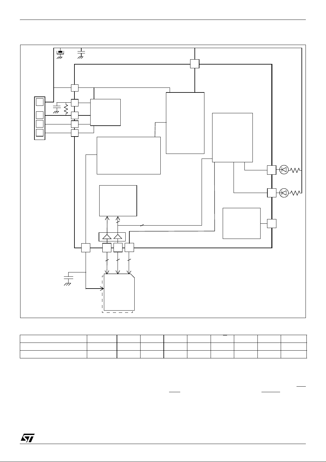
Figure 7. Smartmedia Card Writer Or Flash Drive Application Example
DTC
FLASH
V
DDF
VPP
V
DD
POWER
MANAGEMENT
100nF
12V for
level translator
Flash prog.
REGULATOR
I/O
LOGIC
UP TO 2
SMARTMEDIA
CARDS
PA
PB
V
DD
8
6
I/O
0~7
CTRL
(4)
2
PE
VCC
USB
DP
DM
USBV
DD
USB Port
GND
USB
4.7μF
USBVDD
USB
5V
DP
DM
GND
=4.0-5.5V
100nF
100nF
1.5K
Ω
LED2
LED1
(connect to
GND if
not used)
5
1
ST72651AR6
Table 2. SmartMedia Interface Pin Assignment
SmartMedia Pin I/O0~7 CLE WE ALE RE R/B WP
ST72F65 pin PB0-7 PA0 PA1 PA2 PA3 PA4 PA7 PE1 PE0
ST7 / DTC
(1)
(1): This line shows if the ST72F65 pin is controlled by the
ST7 core or the DTC.
(2): These lines are not controlled by the DTC but by the
user software running on the ST7 core. The ST72F65 pin
choice is at customer discretion. The pins shown here are
only shown as an example.
(3): When a single card is to be handled, PA7 is free for
other functions. When 2 Smartmedia are to be handled,
pins from both cards should be tied together (i.e. CLE1
DTC DTC DTC DTC DTC DTC ST7 ST7 ST7
with CLE2...) except for the CE pins. CE pin from card 1
should be connected to PA6 and CE pin from card 2
should be connect to PA7. Selection of the operating card
is done by ST7 software.
(4) As this is a single power supply application, the USBEN function in not needed. Thus PF4/USBEN pin can be
used as a normal I/O by configuring it as such by the option byte.
Doc ID 7215 Rev 4
(2)
(2)
CE1
CE2
(2)(3)
13/161
1
ST72651AR6
DTC
FLASH
V
DDF
VPP
V
DD
POWER
MANAGEMENT
3)
100nF
level
REGULATOR
I/O
LOGIC
PA
PB
CF
8-BIT MEMORY
MODE
6
8
PE
[2]
translator
LED1
VCC
USB
DP
DM
USBV
DD
USB Port
GND
USB
4.7μF
USBVDD
USB
5V
DP
DM
GND
=4.0-5.5V
100nF
100nF
1.5K
Ω
4.7µF
LED2
12V for
Flash prog.
(connect to
GND if
not used)
5
1
4.7K
Ω
Figure 8. Compact Flash Card Writer Application Example
Table 3. Compact Flash Card Writer Pin Assignment
Compact Flash
Card Pin
D0-7 D8-15
, VS2, WAIT,
VS1
, INPACK,
CS1
BVD1
, BVD2
IORD,
IOWR
CE2
ST72F65 pin PB0-7 NC NC V
1)
ST7 / DTC
Notes:
1. This line shows if the ST72F65 pin is controlled by the
ST7 core or by the DTC.
2. These lines are not controlled by the DTC but by the
DTC - - Power Power DTC ST7 DTC DTC ST7 -
user software running on the ST7 core. The choice of
14/161
1
Doc ID 7215 Rev 4
, REG,
, V
CC
DDF
CSEL,
RESET,
GND,
A3-10
V
ST72F65 pin is at the customer’s discretion. The pins
shown here are given only as an example.
3. As this is a single power supply application, the USBEN
function in not needed. Thus PF4/USBEN pin can be
used as a normal I/O by configuring it as such by the op-
SSF
A0-2 CE1
PE2
PA0-2
+pull-up
4.7kΩ
RE WE CD1
PA6
PA3 PA5
+pull-up
100kΩ
RDY/BSY,
tion byte.
CD2,
WP
NC
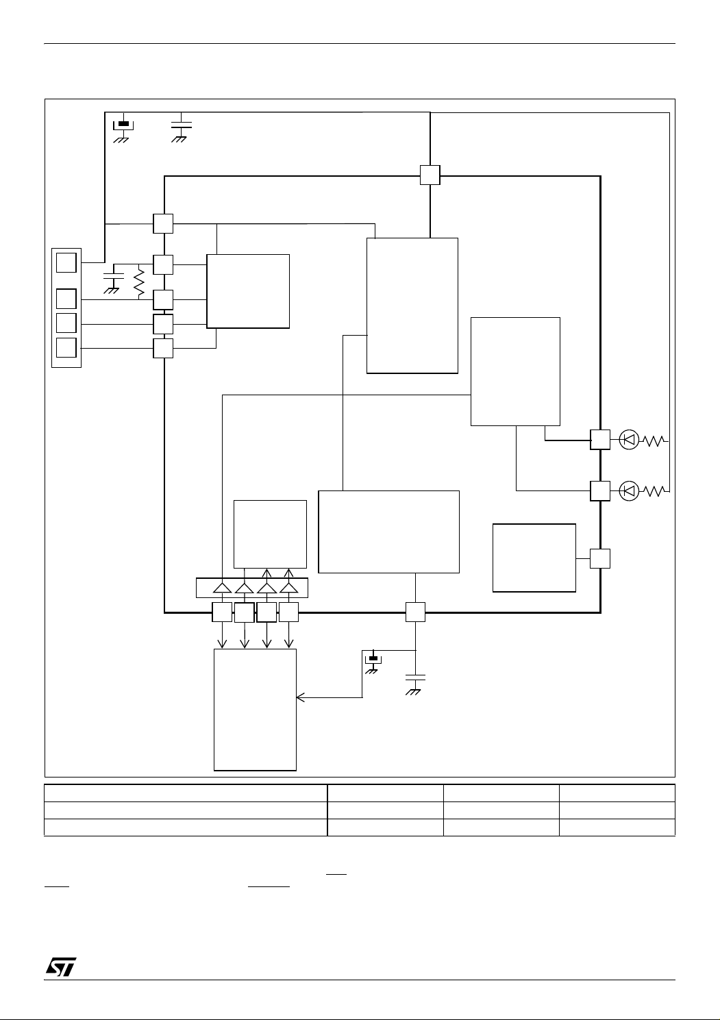
Figure 9. Sony Memory Stick Writer Ap3plication Example
VCC
USB
DP
DM
USBV
DD
DTC
USB Port
FLASH
V
DDF
VPP
GND
USB
4.7μF
V
DD
USBVDD
POWER
USB
MANAGEMENT
2)
5V
DP
DM
GND
100nF
12V for
LED2
level translator
Flash prog.
REGULATOR
I/O
LOGIC
=4.0-5.5V
SONY
MEMORY STICK
PC3
PC1
V
DD
PC2
100nF
100nF
1.5KΩ
LED1
(connect to
GND if
not used)
PC0
CD CLK BS DAT
4.7µF
ST72651AR6
MultiMedia Card Pin CMD DAT CLK
ST72F65 pin PE5 PE6 PE7
ST7 / DTC
(1) This line shows if the ST72F65 pin is controlled by the
(1)
ST7 core or by the DTC.
DTC DTC DTC
used as a normal I/O by configuring it as such by the option byte.
(2) As this is a single power supply application, the USBEN function in not needed. Thus PF4/USBEN pin can be
Doc ID 7215 Rev 4
15/161
1
ST72651AR6
0000h
Interrupt & Reset Vectors
HW Registers
0050h
004Fh
(see Table 4)
FFDFh
FFE0h
FFFFh
(see Table 10)
8000h
7FFFh
Program Memory*
5 KBytes RAM*
16 Kbytes
C000h
Reserved
1450h
144Fh
32 Kbytes
512 Bytes RAM*
Short Addressing
Stack (256 Bytes)
0100h
0200h
144Fh
0050h
00FFh
01FFh
16-bit Addressing RAM
RAM (176 Bytes)
(4688 Bytes)
Short Addressing
Stack (256 Bytes)
0100h
0200h
024Fh
0050h
00FFh
01FFh
16-bit Addressing RAM
RAM (176 Bytes)
(80 Bytes)
154Fh
1A4Fh
256 Bytes
1280 Bytes
USB Data Buffer**
DTC RAM (Write protected)
3 REGISTER & MEMORY MAP
As shown in Figure 10, the MCU is capable of addressing 64 Kbytes of memories and I/O registers.
The available memory locations consist of 80
bytes of register locations, up to 5 Kbytes of RAM
and up to 32 Kbytes of user program memory. The
RAM space includes up to 256 bytes for the stack
from 0100h to 01FFh.
Figure 10. Memory Map
The highest address bytes contain the user reset
and interrupt vectors.
IMPORTANT: Memory locations noted “Reserved” must never be accessed. Accessing a reserved area can have unpredictable effects on the
device.
Related Documentation
AN985: Executing Code in ST7 RAM
* Program memory and RAM sizes are product dependent (see Table –)
** The ST7 core is not able to read or write in the USB data buffer if the ST7265x is running at 6Mz in stan-
dalone mode.
16/161
1
Doc ID 7215 Rev 4

ST72651AR6
Table 4. Hardware Register Memory Map
Address Block Register Label Register name Reset Status Remarks
Port A Data Register
Port A Data Direction Register
Port A Option Register
Port B Data Register
Port B Data Direction Register
Port C Data Register
Port C Data Direction Register
Port C Option Register
Port D Data Register
Port D Data Direction Register
Port D Option Register
Port E Data Register
Port E Data Direction Register
Port E Option Register
Port F Data Register
Port F Data Direction Register
ADC Data Register
ADC Control Status Register
Reserved Area (3 bytes)
SPI Data I/O Register
SPI Control Register
SPI Control/Status Register
DTC Control Register
DTC Status Register
DTC Pointer Register
1
PADR
PADDR
PAOR
PBDR
PBDDR
PCDR
PCDDR
PCOR
PDDR
PDDDR
PDOR
PEDR
PEDDR
PEOR
PFDR
PFDDR
ADCDR
ADCCSR
SPIDR
SPICR
SPICSR
DTCCR
DTCSR
Reserved
DTCPR
0000h
0001h
0002h
0003h
0004h
0005h Reserved Area (1 byte)
0006h
0007h
0008h
0009h
000Ah
000Bh
000Ch
000Dh
000Eh
000Fh
0010h
0011h Reserved Area (1 byte)
0012h
0013h
0014h WDG WDGCR Watchdog Control Register 7Fh R/W
0015h
to
0017h
0018h DSM PCR Power Control Register 00h R/W
0019h
001Ah
001Bh
001Ch
001Dh
001Eh
001Fh
ADC
SPI
DTC
00h
00h
00h
00h
00h
00h
00h
00h
00h
00h
00h
00h
00h
00h
00h
00h
00h
00h
xxh
0xh
00h
00h
00h
00h
R/W
R/W
R/W
R/W
R/W
R/W
R/W
R/W
R/W
R/W
R/W
R/W
R/W
R/W
R/W
R/W
Read only
R/W
R/W
R/W
R/W
R/W
R/W
R/W
Doc ID 7215 Rev 4
17/161
1

ST72651AR6
Address Block Register Label Register name Reset Status Remarks
0020h
0021h
0022h
0023h
0024h
0025h
0026h
0027h
0028h
0029h
002Ah
002Bh Flash Flash Control Status Register 00h R/W
002Ch
002Dh
002Eh
002Fh
0030h
0031h
0032h
0033h
0034h
0035h
0036h
0037h
0038h
0039h
003Ah
003Bh
003Ch
003Dh
003Eh
003Fh
0040h
0041h
0042h
0043h
0044h
0045h
0046h
0047h USB BUFCSR Buffer Control/Status Register 00h R/W
0048h Reserved Area (1 Byte)
0049h MISCR1 Miscellaneous Register 1 00h R/W
004Ah MISCR2 Miscellaneous Register 2 00h R/W
004Bh Reserved Area (1 Byte)
TIM
ITC
USB
2C 1
I
TCR1
TCR2
TSR
CHR
CLR
ACHR
ACLR
OC1HR
OC1LR
OC2HR
OC2LR
ITSPR0
ITSPR1
ITSPR2
ITSPR3
USBISTR
USBIMR
USBCTLR
DADDR
USBSR
EP0R
CNT0RXR
CNT0TXR
EP1RXR
CNT1RXR
EP1TXR
CNT1TXR
EP2RXR
CNT2RXR
EP2TXR
CNT2TXR
I2CCR
I2CSR1
I2CSR2
I2CCCR
Not used
Not used
I2CDR
Timer Control Register 1
Timer Control Register 2
Timer Status Register
Timer Counter High Register
Timer Counter Low Register
Timer Alternate Counter High Register
Timer Alternate Counter Low Register
Timer Output Compare 1 High Register
Timer Output Compare 1 Low Register
Timer Output Compare 2 High Register
Timer Output Compare 2 Low Register
Interrupt Software Priority Register 0
Interrupt Software Priority Register 1
Interrupt Software Priority Register 2
Interrupt Software Priority Register 3
USB Interrupt Status Register
USB Interrupt Mask Register
USB Control Register
Device Address Register
USB Status Register
Endpoint 0 Register
EP 0 Reception Counter Register
EP 0 Transmission Counter Register
Endpoint 1 Register
EP 1 Reception Counter Register
Endpoint 1 Register
EP 1 Transmission Counter Register
Endpoint 2 Register
EP 2 Reception Counter Register
Endpoint 2 Register
EP 2 Transmission Counter Register
2
I
C Control Register
2
I
C Status Register 1
2
I
C Status Register 2
2
I
C Clock Control Register
2
I
C Data Register
00h
00h
00h
FFh
FCh
FFh
FCh
80h
00h
80h
00h
FFh
FFh
FFh
FFh
00h
00h
06h
00h
00h
00h
00h
00h
00h
00h
00h
00h
00h
00h
00h
00h
00h
00h
00h
00h
00h
R/W
R/W
Read Only
Read Only
Read Only
Read Only
Read Only
R/W
R/W
R/W
R/W
R/W
R/W
R/W
R/W
R/W
R/W
R/W
R/W
R/W
R/W
R/W
R/W
R/W
R/W
R/W
R/W
R/W
R/W
R/W
R/W
R/W
Read only
Read only
R/W
R/W
18/161
1
Doc ID 7215 Rev 4

ST72651AR6
Address Block Register Label Register name Reset Status Remarks
004Ch MISCR3 Miscellaneous Register 3 00h R/W
004Dh
004Eh
004Fh
PWM
PWM0
1)
BRM10
PWM1
10-bit PWM/BRM registers
80h
00h
80h
Note 1. If the peripheral is present on the device (see Device Summary on page 1)
R/W
R/W
R/W
Doc ID 7215 Rev 4
19/161
1
ST72651AR6
4 Kbytes
4 Kbytes
2Kbytes
SECTOR 1
SECTOR 0
16 Kbytes
SECTOR 2
8K 16K 32K 60K DV FLASH
FFFFh
EFFFh
DFFFh
3FFFh
7FFFh
1000h
24 Kbytes
MEMORY SIZE
8Kbytes 40 Kbytes
52 Kbytes
9FFFh
BFFFh
D7FFh
4K 10K 24K 48K
4 FLASH PROGRAM MEMORY
4.1 Introduction
The ST7 dual voltage High Density Flash
(HDFlash) is a non-volatile memory that can be
electrically erased as a single block or by individual sectors and programmed on a Byte-by-Byte basis using an external V
supply.
PP
The HDFlash devices can be programmed and
erased off-board (plugged in a programming tool)
or on-board using ICP (In-Circuit Programming) or
IAP (In-Application Programming).
The array matrix organisation allows each sector
to be erased and reprogrammed without affecting
other sectors.
4.2 Main Features
■ Three Flash programming modes:
– Insertion in a programming tool. In this mode,
all sectors including option bytes can be programmed or erased.
– ICP (In-Circuit Programming). In this mode, all
sectors including option bytes can be programmed or erased without removing the device from the application board.
– IAP (In-Application Programming) In this
mode, all sectors except Sector 0, can be programmed or erased without removing the device from the application board and while the
application is running.
■ ICT (In-Circuit Testing) for downloading and
executing user application test patterns in RAM
■ Read-out protection
■ Register Access Security System (RASS) to
prevent accidental programming or erasing
4.3 Structure
Depending on the overall Flash memory size in the
microcontroller device, there are up to three user
sectors (see Table 5). Each of these sectors can
be erased independently to avoid unnecessary
erasing of the whole Flash memory when only a
partial erasing is required.
The first two sectors have a fixed size of 4 Kbytes
(see Figure 11). They are mapped in the upper
part of the ST7 addressing space so the reset and
interrupt vectors are located in Sector 0 (F000hFFFFh).
Table 5. Sectors available in Flash devices
Flash Memory Size
(bytes)
4K Sector 0
8K Sectors 0,1
> 8K Sectors 0,1, 2
Available Sectors
4.4 Read-out Protection
Read-out protection, when selected, provides a
protection against Program Memory content extraction and against write access to Flash memory. Even if no protection can be considered as totally unbreakable, the feature provides a very high
level of protection for a general purpose microcontroller.
In Flash devices, this protection is removed by reprogramming the option. In this case, the entire
program memory is first automatically erased and
the device can be reprogrammed.
Read-out protection selection is enabled and removed through the FMP_R bit in the option byte.
The Flash memory is organised in sectors and can
be used for both code and data storage.
Figure 11. Memory Map and Sector Address
Doc ID 7215 Rev 4
20/161
1
FLASH PROGRAM MEMORY (Cont’d)
ICC CONNECTOR
ICCDATA
ICCCLK
RESET
V
DD
HE10 CONNECTOR TYPE
APPLICATION
POWER SUPPLY
1
246810
975 3
PROGRAMMING TOOL
ICC CONNECTOR
APPLICATION BOARD
ICC Cable
(See Note 3)
10kΩ
V
SS
ICCSEL/VPP
ST7
C
L2
C
L1
OSC1
OSC2
OPTIONAL
See Note 1
See Note 2
APPLICATION
RESET SOURCE
APPLICATION
I/O
(See Note 4)
ST72651AR6
4.5 ICC Interface
ICC needs a minimum of 4 and up to 6 pins to be
connected to the programming tool (see Figure
12). These pins are:
– RESET
–V
: device reset
: device power supply ground
SS
Figure 12. Typical ICC Interface
– ICCCLK: ICC output serial clock pin
– ICCDATA: ICC input/output serial data pin
– ICCSEL/V
: programming voltage
PP
– OSC1(or OSCIN): main clock input for exter-
nal source (optional)
: application board power supply (see Fig-
–V
DD
ure 12, Note 3)
Notes:
1. If the ICCCLK or ICCDATA pins are only used
as outputs in the application, no signal isolation is
necessary. As soon as the Programming Tool is
plugged to the board, even if an ICC session is not
in progress, the ICCCLK and ICCDATA pins are
not available for the application. If they are used as
inputs by the application, isolation such as a serial
resistor has to implemented in case another device forces the signal. Refer to the Programming
Tool documentation for recommended resistor values.
2. During the ICC session, the programming tool
must control the RESET
flicts between the programming tool and the application reset circuit if it drives more than 5mA at
high level (push pull output or pull-up resistor<1K).
A schottky diode can be used to isolate the application RESET circuit in this case. When using a
classical RC network with R>1K or a reset man-
pin. This can lead to con-
agement IC with open drain output and pull-up resistor>1K, no additional components are needed.
In all cases the user must ensure that no external
reset is generated by the application during the
ICC session.
3. The use of Pin 7 of the ICC connector depends
on the Programming Tool architecture. This pin
must be connected when using most ST Programming Tools (it is used to monitor the application
power supply). Please refer to the Programming
Tool manual.
4. Pin 9 has to be connected to the OSC1 or OSCIN pin of the ST7 when the clock is not available
in the application or if the selected clock option is
not programmed in the option byte. ST7 devices
with multioscillator capability need to have OSC2
grounded in this case.
Doc ID 7215 Rev 4
21/161
1

ST72651AR6
FLASH PROGRAM MEMORY (Cont’d)
4.6 ICP (In-Circuit Programming)
To perform ICP the microcontroller must be
switched to ICC (In-Circuit Communication) mode
by an external controller or programming tool.
Depending on the ICP code downloaded in RAM,
Flash memory programming can be fully customized (number of bytes to program, program locations, or selection serial communication interface
for downloading).
When using an STMicroelectronics or third-party
programming tool that supports ICP and the specific microcontroller device, the user needs only to
implement the ICP hardware interface on the application board (see Figure 12). For more details
on the pin locations, refer to the device pinout description.
4.7 IAP (In-Application Programming)
This mode uses a BootLoader program previously
stored in Sector 0 by the user (in ICP mode or by
plugging the device in a programming tool).
This mode is fully controlled by user software. This
allows it to be adapted to the user application, (user-defined strategy for entering programming
mode, choice of communications protocol used to
fetch the data to be stored, etc.). For example, it is
possible to download code from the SPI, SCI, USB
or CAN interface and program it in the Flash. IAP
mode can be used to program any of the Flash
sectors except Sector 0, which is write/erase protected to allow recovery in case errors occur during the programming operation.
4.8 Related Documentation
For details on Flash programming and ICC protocol, refer to the ST7 Flash Programming Reference Manual and to the ST7 ICC Protocol Reference Manual
.
4.9 Register Description
FLASH CONTROL/STATUS REGISTER (FCSR)
Read/Write
Reset Value: 0000 0000 (00h)
70
00000000
This register is reserved for use by Programming
Tool software. It controls the Flash programming
and erasing operations.
Table 6. FLASH Register Map and Reset Values
Address
(Hex.)
002Bh
22/161
Register
Label
FCSR
Reset Value
76543210
00000000
Doc ID 7215 Rev 4
1

5 CENTRAL PROCESSING UNIT
ACCUMULATOR
X INDEX REGISTER
Y INDEX REGISTER
STACK POINTER
CONDITION CODE REGISTER
PROGRAM COUNTER
70
1C1I1HI0NZ
RESET VALUE = RESET VECTOR @ FFFEh-FFFFh
70
70
70
0
7
15 8
PCH
PCL
15
8
70
RESET VALUE = STACK HIGHER ADDRESS
RESET VALUE =
1X11X1XX
RESET VALUE = XXh
RESET VALUE = XXh
RESET VALUE = XXh
X = Undefined Value
ST72651AR6
5.1 INTRODUCTION
This CPU has a full 8-bit architecture and contains
six internal registers allowing efficient 8-bit data
manipulation.
5.2 MAIN FEATURES
■ Enable executing 63 basic instructions
■ Fast 8-bit by 8-bit multiply
■ 17 main addressing modes (with indirect
addressing mode)
■ Two 8-bit index registers
■ 16-bit stack pointer
■ Low power HALT and WAIT modes
■ Priority maskable hardware interrupts
■ Non-maskable software/hardware interrupts
Figure 13. CPU Registers
5.3 CPU REGISTERS
The six CPU registers shown in Figure 13 are not
present in the memory mapping and are accessed
by specific instructions.
Accumulator (A)
The Accumulator is an 8-bit general purpose register used to hold operands and the results of the
arithmetic and logic calculations and to manipulate
data.
Index Registers (X and Y)
These 8-bit registers are used to create effective
addresses or as temporary storage areas for data
manipulation. (The Cross-Assembler generates a
precede instruction (PRE) to indicate that the following instruction refers to the Y register.)
The Y register is not affected by the interrupt automatic procedures.
Program Counter (PC)
The program counter is a 16-bit register containing
the address of the next instruction to be executed
by the CPU. It is made of two 8-bit registers PCL
(Program Counter Low which is the LSB) and PCH
(Program Counter High which is the MSB).
Doc ID 7215 Rev 4
23/161
1

ST72651AR6
CENTRAL PROCESSING UNIT (Cont’d)
Condition Code Register (CC)
Read/Write
Reset Value: 111x1xxx
70
11I1HI0NZ
C
The 8-bit Condition Code register contains the interrupt masks and four flags representative of the
result of the instruction just executed. This register
can also be handled by the PUSH and POP instructions.
These bits can be individually tested and/or controlled by specific instructions.
Arithmetic Management Bits
Bit 4 = H Half carry.
This bit is set by hardware when a carry occurs be-
tween bits 3 and 4 of the ALU during an ADD or
ADC instructions. It is reset by hardware during
the same instructions.
0: No half carry has occurred.
1: A half carry has occurred.
This bit is tested using the JRH or JRNH instruction. The H bit is useful in BCD arithmetic subroutines.
Bit 2 = N Negative.
This bit is set and cleared by hardware. It is repre-
sentative of the result sign of the last arithmetic,
logical or data manipulation. It’s a copy of the re-
th
sult 7
bit.
0: The result of the last operation is positive or null.
1: The result of the last operation is negative
(that is, the most significant bit is a logic 1).
This bit is accessed by the JRMI and JRPL instructions.
Bit 1 = Z Zero.
This bit is set and cleared by hardware. This bit in-
dicates that the result of the last arithmetic, logical
or data manipulation is zero.
0: The result of the last operation is different from
zero.
1: The result of the last operation is zero.
This bit is accessed by the JREQ and JRNE test
instructions.
Bit 0 = C Carry/borrow.
This bit is set and cleared by hardware and software. It indicates an overflow or an underflow has
occurred during the last arithmetic operation.
0: No overflow or underflow has occurred.
1: An overflow or underflow has occurred.
This bit is driven by the SCF and RCF instructions
and tested by the JRC and JRNC instructions. It is
also affected by the “bit test and branch”, shift and
rotate instructions.
Interrupt Management Bits
Bit 5,3 = I1, I0 Interrupt
The combination of the I1 and I0 bits gives the cur-
rent interrupt software priority.
Interrupt Software Priority I1 I0
Level 0 (main) 1 0
Level 1 0 1
Level 2 0 0
Level 3 (= interrupt disable) 1 1
These two bits are set/cleared by hardware when
entering in interrupt. The loaded value is given by
the corresponding bits in the interrupt software priority registers (IxSPR). They can be also set/
cleared by software with the RIM, SIM, IRET,
HALT, WFI and PUSH/POP instructions.
See the interrupt management chapter for more
details.
24/161
1
Doc ID 7215 Rev 4
CENTRAL PROCESSING UNIT (Cont’d)
PCH
PCL
SP
PCH
PCL
SP
PCL
PCH
X
A
CC
PCH
PCL
SP
PCL
PCH
X
A
CC
PCH
PCL
SP
PCL
PCH
X
A
CC
PCH
PCL
SP
SP
Y
CALL
Subroutine
Interrupt
Event
PUSH Y POP Y IRET
RET
or RSP
@ 01FFh
@ 0100h
Stack Higher Address = 01FFh
Stack Lower Address =
0100h
ST72651AR6
Stack Pointer (SP)
Read/Write
Reset Value: 01 FFh
15 8
00000001
The least significant byte of the Stack Pointer
(called S) can be directly accessed by a LD instruction.
Note: When the lower limit is exceeded, the Stack
Pointer wraps around to the stack upper limit, without indicating the stack overflow. The previously
stored information is then overwritten and therefore lost. The stack also wraps in case of an underflow.
70
SP7 SP6 SP5 SP4 SP3 SP2 SP1
SP0
The stack is used to save the return address during a subroutine call and the CPU context during
an interrupt. The user may also directly manipulate
the stack by means of the PUSH and POP instruc-
The Stack Pointer is a 16-bit register which is always pointing to the next free location in the stack.
It is then decremented after data has been pushed
onto the stack and incremented before data is
popped from the stack (see Figure 14).
Since the stack is 256 bytes deep, the 8 most significant bits are forced by hardware. Following an
MCU Reset, or after a Reset Stack Pointer instruction (RSP), the Stack Pointer contains its reset value (the SP7 to SP0 bits are set) which is the stack
tions. In the case of an interrupt, the PCL is stored
at the first location pointed to by the SP. Then the
other registers are stored in the next locations as
shown in Figure 14.
– When an interrupt is received, the SP is decre-
mented and the context is pushed on the stack.
– On return from interrupt, the SP is incremented
and the context is popped from the stack.
A subroutine call occupies two locations and an interrupt five locations in the stack area.
higher address.
Figure 14. Stack Manipulation Example
Doc ID 7215 Rev 4
25/161
1
ST72651AR6
OSCIN
OSCOUT
EXTERNAL
CLOCK
NC
OSCIN
OSCOUT
C
OSCIN
C
OSCOUT
6 SUPPLY, RESET AND CLOCK MANAGEMENT
6.1 CLOCK SYSTEM
6.1.1 General Description
The MCU accepts either a 12 MHz crystal or an
external clock signal to drive the internal oscillator.
The internal clock (f
nal oscillator frequency (f
) is derived from the inter-
CPU
), which is 12 Mhz in
OSC
Stand-alone mode and 48Mhz in USB mode.
The internal clock (f
) is software selectable us-
CPU
ing the CP[1:0] and CPEN bits in the MISCR1 register.
In USBV
power supply mode, the PLL is active,
DD
generating a 48MHz clock to the USB. In this
mode, f
In V
DD
bled, and the maximum frequency of f
can be configured to be up to 8 MHz.
CPU
mode the PLL and the USB clock are disa-
is 6
CPU
MHz.
The internal clock signal (f
) is also routed to
CPU
the on-chip peripherals. The CPU clock signal
consists of a square wave with a duty cycle of
50%.
The internal oscillator is designed to operate with
an AT-cut parallel resonant quartz in the frequency
range specified for f
. The circuit shown in Fig-
osc
ure 16 is recommended when using a crystal, and
Table 7 lists the recommended capacitance. The
crystal and associated components should be
mounted as close as possible to the input pins in
order to minimize output distortion and start-up
stabilisation time.
6.1.2 External Clock
An external clock may be applied to the OSCIN input with the OSCOUT pin not connected, as
shown on Figure 15. The t
specifications
OXOV
does not apply when using an external clock input.
The equivalent specification of the external clock
source should be used instead of t
OXOV
(see Sec-
tion 6.5 CONTROL TIMING).
Figure 15. External Clock Source Connections
Figure 16. Crystal Resonator
Table 7. Recommended Values for 12-MHz
Crystal Resonator
R
SMAX
C
OSCIN
C
OSCOUT
Note: R
crystal (see crystal specification).
26/161
SMAX
1
20 Ω 25 Ω 70 Ω
56pF 47pF 22pF
56pF 47pF 22pF
is the equivalent serial resistor of the
Doc ID 7215 Rev 4
6.2 RESET SEQUENCE MANAGER (RSM)
V
DD
RUN
RESET PIN
EXTERNAL
WATCHDOG
ACTIVE PHASE
V
IT+(LVD)
V
IT-(LVD)
t
h(RSTL)in
t
w(RSTL)out
RUN
t
h(RSTL)in
ACTIVE
WATCHDOG UNDERFLOW
t
w(RSTL)out
RUN RUN RUN
RESET
RESET
SOURCE
SHORT EXT.
RESET
LVD
RESET
LONG EXT.
RESET
WATCHDOG
RESET
INTERNAL RESET (min 512 T
CPU
)
VECTOR FETCH
t
w(RSTL)out
PHASE
ACTIVE
PHASE
ACTIVE
PHASE
DELAY
ST72651AR6
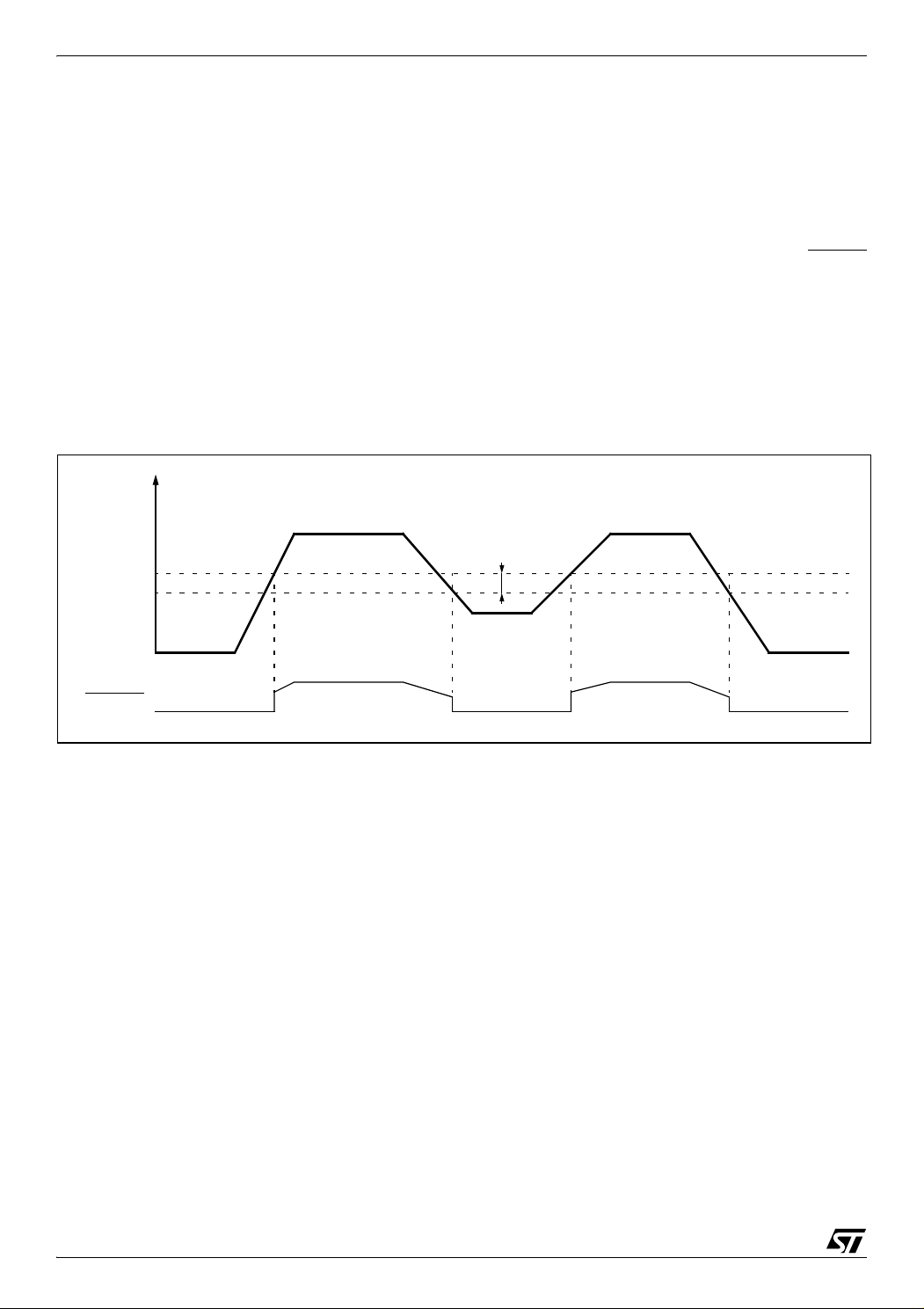
6.2.1 Introduction
The reset sequence manager includes three RESET sources as shown in Figure 6.2.2:
■ External RESET source pulse
■ Internal LVD RESET (Low Voltage Detection)
■ Internal WATCHDOG RESET
These sources act on the RESET
pin and it is al-
ways kept low during the delay phase.
The RESET service routine vector is fixed at ad-
dresses FFFEh-FFFFh in the ST7 memory map.
Figure 17. RESET Sequences
The basic RESET sequence consists of 3 phases
as shown in Figure 17:
■ Active Phase depending on the RESET source
■ Min 512 CPU clock cycle delay (see Figure 19
and Figure 20
■ RESET vector fetch
Caution: When the ST7 is unprogrammed or fully
erased, the Flash is blank and the RESET vector
is not programmed. For this reason, it is recommended to keep the RESET pin in low state until
programming mode is entered, in order to avoid
unwanted behaviour.
Doc ID 7215 Rev 4
27/161
1
ST72651AR6
f
CPU
COUNTER
RESET
R
ON
V
DD
WATCHDOG RESET
LVD RESET
INTERNAL
RESET
PULSE
GENERATOR
RESET SEQUENCE MANAGER (Cont’d)
6.2.2 Asynchronous External RESET
The RESET
output with integrated R
pin is both an input and an open-drain
weak pull-up resistor.
ON
pin
This pull-up has no fixed value but varies in accordance with the input voltage. It
can be pulled
low by external circuitry to reset the device. See
electrical characteristics section for more details.
A RESET signal originating from an external
source must have a duration of at least t
h(RSTL)in
in
order to be recognized. This detection is asynchronous and therefore the MCU can enter reset state
even in HALT mode.
The RESET
pin is an asynchronous signal which
plays a major role in EMS performance. In a noisy
environment, it is recommended to follow the
guidelines mentioned in the electrical characteristics section.
If the external RESET
t
w(RSTL)out
(see short ext. Reset in Figure 17), the
signal on the RESET
pulse is shorter than
pin will be stretched. Otherwise the delay will not be applied (see long ext.
Reset in Figure 17).
Figure 18. Reset Block Diagram
Starting from the external RESET pulse recognition, the device RESET
is pulled low during at least t
pin acts as an output that
w(RSTL)out
.
6.2.3 Internal Low Voltage Detection RESET
Two different RESET sequences caused by the internal LVD circuitry can be distinguished:
■
Power-On RESET
■ Voltage Drop RESET
The device RESET
pulled low when V
V
DD<VIT-
(falling edge) as shown in Figure 17.
The LVD filters spikes on V
pin acts as an output that is
DD<VIT+
(rising edge) or
shorter than t
DD
g(VDD)
to avoid parasitic resets.
6.2.4 Internal Watchdog RESET
The RESET sequence generated by a internal
Watchdog counter overflow is shown in Figure 17.
Starting from the Watchdog counter underflow, the
device RESET
low during at least t
pin acts as an output that is pulled
w(RSTL)out
.
28/161
1
Doc ID 7215 Rev 4
RESET SEQUENCE MANAGER (Cont’d)
512 x t
CPU(STAND-ALONE)
RESET
FETCH VECTOR
DELAY
FETCH VECTOR
256 x t
CPU(STAND-ALONE)
256 x t
CPU(USB)
PLL Startup
RESET
time (undefined)
DELAY
400 µs typ.
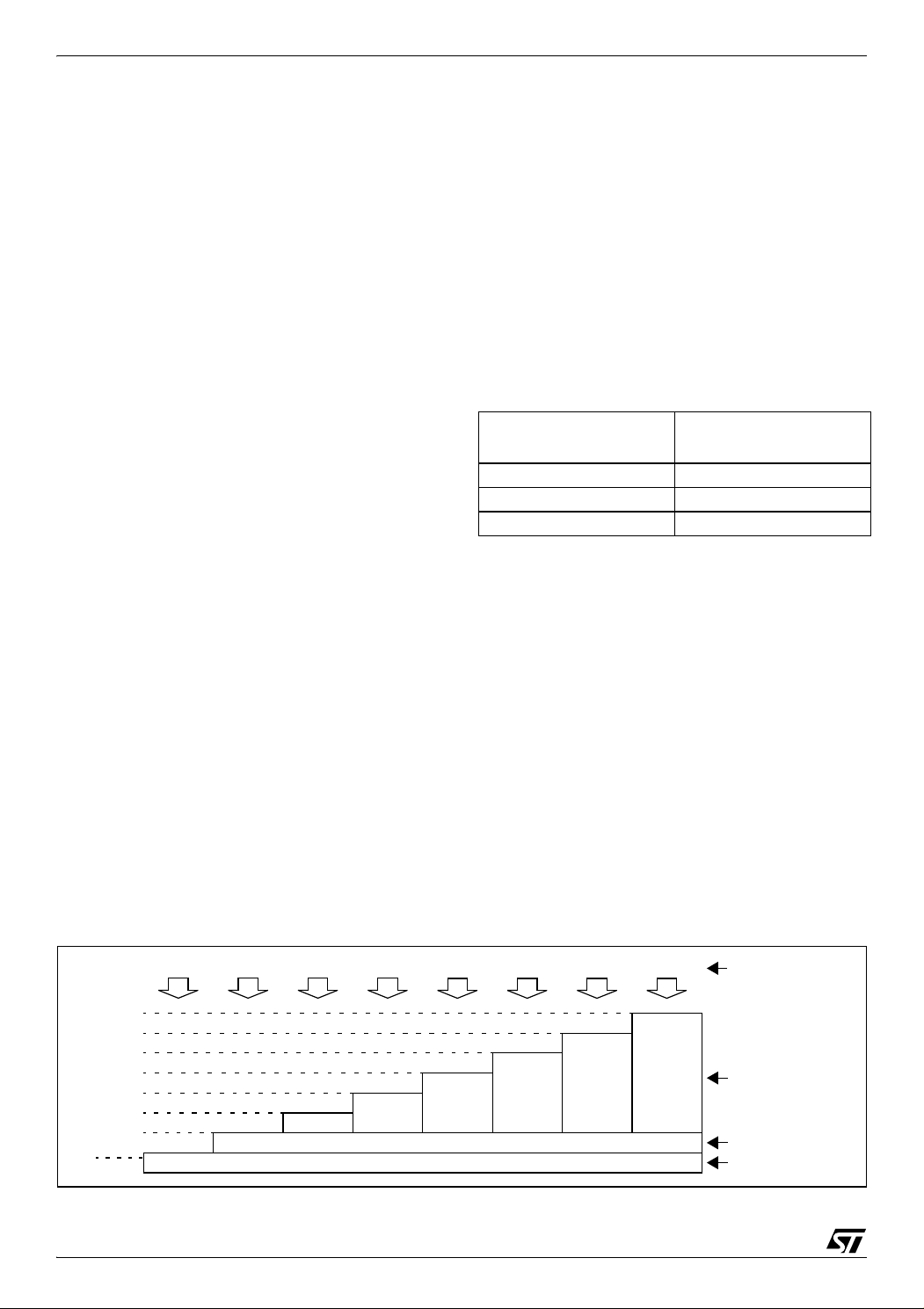
In stand-alone mode, the 512 CPU clock cycle delay allows the oscillator to stabilize and ensures
that recovery has taken place from the Reset
state.
Figure 19. Reset Delay in Stand-alone Mode
Figure 20. Reset Delay in USB Mode
ST72651AR6
In USB mode the delay is 256 clock cycles counted from when the PLL LOCK signal goes high.
The RESET vector fetch phase duration is 2 clock
cycles.
Note: For a description of Stand-alone mode and USB mode refer to Section 6.4.
Doc ID 7215 Rev 4
29/161
1
ST72651AR6
V
DDA
V
IT+(LVD)
RESET
V
IT-(LVD)
V
hyst
6.3 LOW VOLTAGE DETECTOR (LVD)
To allow the integration of power management
features in the application, the Low Voltage Detector function (LVD) generates a static reset when
the V
supply voltage is below a V
DDA
reference
IT-
value. This means that it secures the power-up as
well as the power-down, keeping the ST7 in reset.
The V
than the V
reference value for a voltage drop is lower
IT-
reference value for power-on in order
IT+
to avoid a parasitic reset when the MCU starts running and sinks current on the supply (hysteresis).
Figure 21. Low Voltage Detector vs Reset
The LVD Reset circuitry generates a reset when
is below:
V
DDA
–V
–V
when V
IT+
when V
IT-
DDA
is falling
DDA
is rising
The LVD function is illustrated in Figure 21.
During a Low Voltage Detector Reset, the RESET
pin is held low, thus permitting the MCU to reset
other devices.
Note: It is recommended to make sure that the
supply voltage rises monotonously when the
V
DDA
device is exiting from Reset, to ensure the application functions properly.
30/161
1
Doc ID 7215 Rev 4

6.4 POWER SUPPLY MANAGEMENT
V
DD1
V
DD2
V
DDA
USBV
DD
ST7
4.0 - 5.5 V
Note: Ground lines not shown
ST72651AR6
6.4.1 Single Power Supply Management
In applications operating only when connected to
the USB (Flash writers, Backup systems), the microcontroller must operate from a single power
supply (i.e. USB bus power supply or the local
power source in the case of self-powered devices). Devices with LVD (no E suffix) or without LVD
(E suffix) can support this configuration.
In order to enable the Single Power Supply Management, the PLGIE bit in the PCR register should
kept cleared by software (reset default value).
In this case, pin V
and USBVDD of the micro-
DD
controller must be connected together and supplied by a 4.0 to 5.5V voltage supply, either from
the USB cable or from the local power source. See
Figure 22.
Figure 22. Single Power Supply Mode
.
In this mode:
– The PLL is running at 48 MHz
– The on-chip USB interface is enabled
– The core can run at up to 8MHz internal frequen-
cy
– The microcontroller can be either USB bus pow-
ered or supplied by the local power source (self
powered)
– The USBEN
function is not used. The PF4 pin
can be configured to work as a normal I/O by programming the Option Byte.
6.4.2 Dual Power Supply Management
In case of a device that can be used both when
powered by the USB or from a battery (Digital Audio Player, Digital Camera, PDA), the microcontroller can operate in two power supply modes:
Stand-alone Mode and USB Mode. This configuration is only available on devices without LVD (E
suffix). Devices with LVD are kept under reset
when the power supply drops below the LVD
threshold voltage and thus Stand-Alone mode can
not be entered.
In order to enable Dual Power Supply Management:
– the USBEN
pin function must be selected by pro-
gramming the option byte.
– the user software must set the PLGIE bit in the
PCR register in the initialization routine.
Stand-Alone Mode
This mode is to be used when no USB communication is needed. The microcontroller in this mode
can run at very low voltage, making the design of
low power / battery supplied systems easy. In this
mode:
– The USB cable is unplugged (no voltage input on
DD
pin)
USBV
– The PLL is off
– The on-chip USB interface is disabled
– The core can run at up to 6 MHz internal frequen-
cy
– The DTC operates at a frequency of 6MHz
– USBEN
– The microcontroller is supplied through the V
is kept floating by H/W.
DD
pin
USB Mode
When connected to the USB, the microcontroller
can run at full speed, still saving battery power by
using USB power or self power source. To go into
USB mode, a voltage from 4.0V to 5.5V must be
provided to the USBV
pin. In this mode:
DD
– The USB cable is plugged in
– USBV
pin is supplied by a 4.0 to 5.5V supply
DD
voltage, either from the USB cable or from the
self powering source
– The PLL is running at 48 MHz
– The on-chip USB interface is enabled
– The core can run at up to 8 MHz internal frequen-
cy
– The DTC operates at a frequency of 24MHz
– USBEN
is set to output low level by hardware.
This signal can be used to control an external
transistor (USB SWITCH) to change the power
supply configuration (see Figure 23).
– The microcontroller can be USB bus powered
Doc ID 7215 Rev 4
31/161
1

ST72651AR6
V
DD1
USB SWITCH
V
DD2
V
DDA
USBV
DD
USBEN
ST7
(True OD, H/W ctrl)
Step-up converter (Note 3)
4V min. from USB
Note 1: Ground lines not shown
PCR REGISTER
PLG
General Purpose I/O (I/O port DR, DDR)
Option bit
USBEN H/W
CONTROL
USBV
IT-
USBV
IT+
USBV
IT-
PLG bit
USBV
DD
Alternate Function (USBEN)
VITPF
USBV
IT+
VITMF Bit
VITPF Bit
PLGIE
VITMF
Interrupt Request
RESET
LOGIC
S/W RESET
EDGE DETECTOR
USB VOLTAGE
DETECTOR
WITH LATCH
DETEN
Note 2: Suggested device: STN3PF06 (STMicroelectronics)
V
DDF
PLL
REGULATOR
Note 3: To allow USB cable unplug detection, output voltage of step-up converter should be low
enough to not enduce (through PMOS substrate diode) voltage greater than USBV
IT-
on USBV
DD
pin
PMOS
(Note 2)
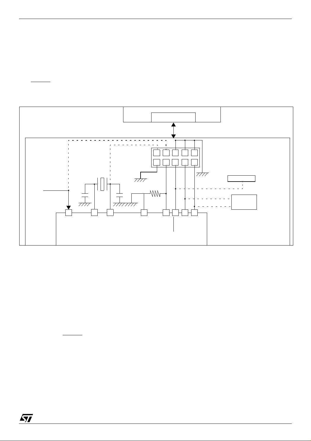
POWER SUPPLY MANAGEMENT (Cont’d)
6.4.2.1 Switching from Stand-Alone Mode to
USB Mode
In Stand-Alone Mode, when the user plugs in the
USB cable, 4V min. is input to USBV
chip power Supply Manager generates an internal
interrupt when USBV
reaches USBV
DD
PLGIE bit in the PCR register is set). The user program then can finish the current processing, and
MUST generate a software RESET
This puts the microcontroller into reset state and
all I/O ports go into input high impedance mode.
Figure 23. External Power Supply Switch
. The on-
DD
(if the
IT+
afterwards.
During and after this (software induced) reset
phase, the USBEN
pin is set to output low level by
hardware. This causes the USB SWITCH to be
turned ON. Consequently, V
USBV
supply. See Figure 23.
DD
pin is powered by
DD
Once in USB mode, no power is drawn from the
step-up converter output.
For more details, refer to Figure 24.
32/161
1
Doc ID 7215 Rev 4

POWER SUPPLY MANAGEMENT (Cont’d)
6.4.2.2 Switching from USB Mode to StandAlone Mode
In USB Mode, when the user unplugs the USB cable, the voltage level drops on the USBV
DD
line.
The on-chip Power Supply Manager generates a
PLG interrupt when USBV
reaches USBV
DD
IT-
The user program then can finish the current
processing, and MUST generate a software RESET.
Caution: Care should be taken as during this period the microcontroller clock is provided from the
PLL output. Functionality in this mode is not guaranteed for voltages below V
Caution: When the V
is supplied externally by
DDF
PLLmin
.
a voltage higher than the detector thresholds, the
USBV
tection diode between V
voltage continues to be driven by the pro-
DD
and USBVDD. In this
DDF
configuration, the detector will not detect a voltage
drop and can not be used.
Software must ensure that the software RESET
generated before V
. drops below V
DD
PLLmin
is
. Failing to do this will cause the clock circuitry to stop,
freezing the microcontroller operations.
ST72651AR6
Once the user program has executed the software
reset, the microcontroller goes into reset state and
all I/O ports go into floating input mode.
During and after this (software induced) reset
phase, the USBEN
.
hardware. It causes the USB SWITCH to be
turned OFF, so USBV
. The PLL is automatically stopped and the in-
V
DD
ternal frequency is provided by a division of the
crystal frequency. Refer to Figure 24.
The microcontroller is still powered by the residual
USBV
voltage (higher than step-up converter
DD
set output level). This V
ing the reset phase until it reaches the step-up
converter set output voltage. At that time, step-up
converter resumes operation, and powers the application.
Caution: In order to avoid applying excessive voltage to the Storage Media, a minimum delay must
be ensured during (and after if needed) the reset
phase, prior to switching ON the external STORAGE switch.
pin is put in high impedance by
is disconnected from
DD
voltage decreases dur-
DD
Doc ID 7215 Rev 4
33/161
1

ST72651AR6
USB MODE
STAND-ALONE STAND-ALONE
RESET
S/W
STAND-ALONE
USBV
DD
V
DD
pin
PLL
48 MHz
CLOCK
CRYSTAL (12MHz)
PLL
CRYSTAL (12MHz)
S/W Reset
PLG INTERRUPT
ON
SUPPLY
USBV
IT+
REQUEST
USBV
IT-
STATUS
PROCESSING
12
1. Interrupt processing
2. Finish current processing
PROCESS.
STAND-ALONE
1
2
S/W Reset
PROCESSING
STAND-ALONE MODE
USBEN
HI-Z HI-Z
voltage
SUPPLY
VOLTAGES
SOURCE
PLL OFF PLL ON PLL OFF
STABLE 48 MHz
UNDE
SIGNAL
ON/OFF
FINED
3
NO CLOCK
3. PLL start-up time (automatically controlled by hardware following a software reset)
USB MODE
NO CLOCK
V
PLLmin48
RESET
RESET
RESET
V
IT+(LVD)
V
IT-(LVD)
RST
4
4. PLL running with frequency in the range of 48 to 24 MHz (see section 13.3.3 on page 127)
POWER SUPPLY MANAGEMENT (Cont’d)
Figure 24. Power Supply Management: Dual Power Supply
34/161
1
Doc ID 7215 Rev 4

POWER SUPPLY MANAGEMENT (Cont’d)
6.4.3 Storage Media Interface I/Os
The microcontroller is able to drive Storage Media
through an interface operating at a different voltage from the rest of the circuit.
This is achieved by powering the Storage Media
interface I/O circuitry through a specific supply rail
connected to V
pin. The V
DDF
pin can be used
DDF
either as an input or output.
If the on-chip voltage regulator is off, power to the
interface I/Os should be provided externally to the
pin. This should be the case when in Stand-
V
DDF
Alone Mode, or in USB mode when the current required to power the Storage Media is above the
current capacity of the on-chip regulator.
If the on-chip voltage regulator is on, it powers the
interface I/Os, and V
pin can supply the Stor-
DDF
age Media. This is recommended in USB Mode,
when the current required to power the Storage
Media is within the capacity of the on-chip regulator.
Caution: If VDDF is supplied externally, the regulator must not be enabled.
Important Note:
If V
is not present, all V
DDF
-driven I/Os cannot
DDF
be used and are tied to ground. Refer to Section
9.2.4 for more details.
Application Example:
Stand-Alone Mode
– The Storage Media interface supply is powered
by V
nects V
enabled by an external switch which con-
DD
DD
to V
. This switch can be driven by
DDF
any True Open Drain I/O pin and controlled by
user software.
ST72651AR6
– The on-chip voltage regulator must be disabled
to avoid any conflict and to decrease consumption (reset the REGEN bit in the PCR register).
USB Mode
– In this case the core of the microcontroller is run-
ning from the USB bus power or the self power
supply. V
a voltage from 4.0 to 5.5V.
– The Storage Media Interface can be powered
through the on-chip regulator (providing power to
the I/O pins and output on pin V
requirement is within the output capacity of the
on chip regulator.
– The regulator output voltage can be pro-
grammed to 2.8V, 3.3V, 3.4V or 3.5 Volts, depending on the Storage Media specifications.
(see VSET[1:0] bits in PCR register description)
– Should the current requirement for the Storage
Media be higher than the current capacity of the
on chip regulator, an external regulator should be
used. Thus the on-chip voltage regulator must be
disabled to avoid any conflict (reset the REGEN
bit in the PCR register).
Caution: The user should ensure that V
not exceed the maximum rating specified for the
Storage Media V
AGE switch on.
and USBVDD pins are supplied with
DD
) if the current
DDF
DD
max when switching STOR-
DDF
does
Doc ID 7215 Rev 4
35/161
1

ST72651AR6
POWER SUPPLY MANAGEMENT (Cont’d)
6.4.4 Register Description
POWER CONTROL REGISTER (PCR)
Reset Value: 0000 0000 (00h)
70
ITPF
ITM
F
PLG IEVSET1VSET0DET
PLG
EN
REG
EN
Bit 7 = ITPF Voltage Input Threshold Plus Flag
This bit is set by hardware when USBV
over USBV
drops below USBV
BV
DD
0: USBV
1:USBVDD > USBV
and cleared by hardware when US-
IT+
< USBV
DD
IT+
IT+
IT+
.
DD
rises
Bit 6 = ITMF Voltage Input Threshold Minus Flag
This bit is set by hardware when USBV
over USBV
drops below USBV
BV
DD
0: USBV
1:USBVDD > USBV
and cleared by hardware when US-
IT-
< USBV
DD
IT-
IT-
IT-
.
DD
rises
Bit 5 = PLG USB Plug/Unplug detection.
This bit is set by hardware when it detects that the
USB cable has been plugged in. It is cleared by
hardware when the USB cable is unplugged. (Detection happens when USBV
or when USBV
V
IT+
drops below USBV
DD
rises over USB-
DD
IT-
). If
the PLGIE bit is set, the rising/falling edge of the
PLG bit also generates an interrupt request. This
interrupt is able to wake up the ST7 core from Halt
mode.
0: USB cable unplugged
1: USB cable plugged in
Bit 3:2 = VSET[1:0] Voltage Regulator Output
Voltage.
These bits are set and cleared by software to select the output voltage of the on-chip voltage regulator (for the V
VSET1VSE
T0
0 0 3.5V
0 1 3.4V
1 0 3.3V
1 1 2.8V
Bit 1 = DETEN
output).
DDF
Voltage output of the regulator
USB Voltage Detector Enable.
This bit is set and cleared by software. It is used to
power-off the USB voltage detector in Stand-alone
mode to reduce unnecessary power consumption,
especially in HALT mode.
0: The USB voltage detector is enabled.
1: The USB voltage detector disabled (ITPF, ITMF
and PLG bits are forced high)
Bit 0 = REGEN Voltage Regulator Enable.
This bit is set and cleared by software.
0: The regulator is completely shutdown and no
current is drawn from the power supply by the
voltage reference.
1: The on-chip voltage regulator is powered-on.
Related Documentation
AN1529: Extending the current & voltage capability on the ST7265 VDDF Supply
Bit 4 = PLGIE USB Plug/Unplug Interrupt Enable.
This bit is set and cleared by software.
0: Single supply mode: PLG interrupt disabled.
1: Dual supply mode: PLG interrupt enabled (gen-
erates an interrupt on the rising/falling edge of
PLG).
36/161
Doc ID 7215 Rev 4
1

7 INTERRUPTS
“IRET”
RESTORE PC, X, A, CC
STACK PC, X, A, CC
LOAD I1:0 FROM INTERRUPT SW REG.
FETCH NEXT
RESET
TLI
PENDING
INSTRUCTION
I1:0
FROM STACK
LOAD PC FROM INTERRUPT VECTOR
Y
N
Y
N
Y
N
Interrupt has the same or a
lower software priority
THE INTERRUPT
STAYS PENDING
than current one
Interrupt has a higher
software priority
than current one
EXECUTE
INSTRUCTION
INTERRUPT
ST72651AR6
7.1 INTRODUCTION
The CPU enhanced interrupt management provides the following features:
■ Hardware interrupts
■ Software interrupt (TRAP)
■ Nested or concurrent interrupt management
with flexible interrupt priority and level
management:
– Up to 4 software programmable nesting levels
– Up to 16 interrupt vectors fixed by hardware
– 3 non maskable events: RESET, TRAP, TLI
This interrupt management is based on:
– Bit 5 and bit 3 of the CPU CC register (I1:0),
– Interrupt software priority registers (ISPRx),
– Fixed interrupt vector addresses located at the
high addresses of the memory map (FFE0h to
FFFFh) sorted by hardware priority order.
This enhanced interrupt controller guarantees full
upward compatibility with the standard (not nested) CPU interrupt controller.
7.2 MASKING AND PROCESSING FLOW
The interrupt masking is managed by the I1 and I0
bits of the CC register and the ISPRx registers
which give the interrupt software priority level of
each interrupt vector (see Table 8). The processing flow is shown in Figure 25.
When an interrupt request has to be serviced:
– Normal processing is suspended at the end of
the current instruction execution.
– The PC, X, A and CC registers are saved onto
the stack.
– I1 and I0 bits of CC register are set according to
the corresponding values in the ISPRx registers
of the serviced interrupt vector.
– The PC is then loaded with the interrupt vector of
the interrupt to service and the first instruction of
the interrupt service routine is fetched (refer to
“Interrupt Mapping” table for vector addresses).
The interrupt service routine should end with the
IRET instruction which causes the contents of the
saved registers to be recovered from the stack.
Note: As a consequence of the IRET instruction,
the I1 and I0 bits will be restored from the stack
and the program in the previous level will resume.
Table 8. Interrupt Software Priority Levels
Interrupt software priority Level I1 I0
Level 0 (main)
Level 1 0 1
Level 2 0 0
Level 3 (= interrupt disable) 1 1
Low
High
10
Figure 25. Interrupt Processing Flowchart
Doc ID 7215 Rev 4
37/161
1

ST72651AR6
PENDING
SOFTWARE
Different
INTERRUPTS
Same
HIGHEST HARDWARE
PRIORITY SERVICED
PRIORITY
HIGHEST SOFTWARE
PRIORITY SERVICED
INTERRUPTS (Cont’d)
Servicing Pending Interrupts
As several interrupts can be pending at the same
time, the interrupt to be taken into account is determined by the following two-step process:
– the highest software priority interrupt is serviced,
– if several interrupts have the same software pri-
ority then the interrupt with the highest hardware
priority is serviced first.
Figure 26 describes this decision process.
Figure 26. Priority Decision Process
When an interrupt request is not serviced immediately, it is latched and then processed when its
software priority combined with the hardware priority becomes the highest one.
Note 1: The hardware priority is exclusive while
the software one is not. This allows the previous
process to succeed with only one interrupt.
Note 2: RESET, TRAP and TLI can be considered
as having the highest software priority in the decision process.
Different Interrupt Vector Sources
Two interrupt source types are managed by the
CPU interrupt controller: the non-maskable type
(RESET, TRAP, TLI) and the maskable type (external or from internal peripherals).
Non-Maskable Sources
These sources are processed regardless of the
state of the I1 and I0 bits of the CC register (see
Figure 25). After stacking the PC, X, A and CC
registers (except for RESET), the corresponding
vector is loaded in the PC register and the I1 and
I0 bits of the CC are set to disable interrupts (level
3). These sources allow the processor to exit
HALT mode.
■ TLI (Top Level Hardware Interrupt)
This hardware interrupt occurs when a specific
edge is detected on the dedicated TLI pin.
Caution: A TRAP instruction must not be used in a
TLI service routine.
■ TRAP (Non Maskable Software Interrupt)
This software interrupt is serviced when the TRAP
instruction is executed. It will be serviced according to the flowchart in Figure 25 as a TLI.
Caution: TRAP can be interrupted by a TLI.
■ RESET
The RESET source has the highest priority in the
CPU. This means that the first current routine has
the highest software priority (level 3) and the highest hardware priority.
See the RESET chapter for more details.
Maskable Sources
Maskable interrupt vector sources can be serviced
if the corresponding interrupt is enabled and if its
own interrupt software priority (in ISPRx registers)
is higher than the one currently being serviced (I1
and I0 in CC register). If any of these two conditions is false, the interrupt is latched and thus remains pending.
■ External Interrupts
External interrupts allow the processor to exit from
HALT low power mode.
External interrupt sensitivity is software selectable
through the ISx bits in the MISCR1 and MISCR3
registers.
External interrupt triggered on edge will be latched
and the interrupt request automatically cleared
upon entering the interrupt service routine.
If several input pins of a group connected to the
same interrupt line are selected simultaneously,
these will be logically NANDed.
■ Peripheral Interrupts
Usually the peripheral interrupts cause the Device
to exit from HALT mode except those mentioned in
the “Interrupt Mapping” table.
A peripheral interrupt occurs when a specific flag
is set in the peripheral status registers and if the
corresponding enable bit is set in the peripheral
control register.
The general sequence for clearing an interrupt is
based on an access to the status register followed
by a read or write to an associated register.
Note: The clearing sequence resets the internal
latch. A pending interrupt (i.e. waiting for being
serviced) will therefore be lost if the clear sequence is executed.
38/161
1
Doc ID 7215 Rev 4

INTERRUPTS (Cont’d)
MAIN
IT4
IT2
IT1
TLI
IT1
MAIN
IT0
I1
HARDWARE PRIORITY
SOFTWARE
3
3
3
3
3
3/0
3
11
11
11
11
11
11 / 10
11
RIM
IT2
IT1
IT4
TLI
IT3
IT0
IT3
I0
10
PRIORITY
LEVEL
USED STACK = 10 BYTES
MAIN
IT2
TLI
MAIN
IT0
IT2
IT1
IT4
TLI
IT3
IT0
HARDWARE PRIORITY
3
2
1
3
3
3/0
3
11
00
01
11
11
11
RIM
IT1
IT4
IT4
IT1
IT2
IT3
I1 I0
11 / 10
10
SOFTWARE
PRIORITY
LEVEL
USED STACK = 20 BYTES
ST72651AR6
7.3 INTERRUPTS AND LOW POWER MODES
All interrupts allow the processor to exit the WAIT
low power mode. On the contrary, only external
and other specified interrupts allow the processor
to exit from the HALT modes (see column “Exit
from HALT” in “Interrupt Mapping” table). When
several pending interrupts are present while exiting HALT mode, the first one serviced can only be
an interrupt with exit from HALT mode capability
and it is selected through the same decision process shown in Figure 26.
Note: If an interrupt, that is not able to Exit from
HALT mode, is pending with the highest priority
when exiting HALT mode, this interrupt is serviced
after the first one serviced.
Figure 27. Concurrent Interrupt Management
7.4 CONCURRENT & NESTED MANAGEMENT
The following Figure 27 and Figure 28 show two
different interrupt management modes. The first is
called concurrent mode and does not allow an interrupt to be interrupted, unlike the nested mode in
Figure 28. The interrupt hardware priority is given
in this order from the lowest to the highest: MAIN,
IT4, IT3, IT2, IT1, IT0, TLI. The software priority is
given for each interrupt.
Warning: A stack overflow may occur without notifying the software of the failure.
Figure 28. Nested Interrupt Management
Doc ID 7215 Rev 4
39/161
1

ST72651AR6
INTERRUPTS (Cont’d)
7.5 INTERRUPT REGISTER DESCRIPTION
INTERRUPT SOFTWARE PRIORITY REGISTERS (ISPRX)
CPU CC REGISTER INTERRUPT BITS
Read/Write
Reset Value: 111x 1010 (xAh)
70
11I1 H I0 NZC
Bit 5, 3 = I1, I0 Software Interrupt Priority
These two bits indicate the current interrupt soft-
ware priority.
Interrupt Software Priority Level I1 I0
Level 0 (main)
Level 1 0 1
Level 2 0 0
Level 3 (= interrupt disable*) 1 1
Low
High
10
These two bits are set/cleared by hardware when
entering in interrupt. The loaded value is given by
the corresponding bits in the interrupt software priority registers (ISPRx).
They can be also set/cleared by software with the
RIM, SIM, HALT, WFI, IRET and PUSH/POP instructions (see “Interrupt Dedicated Instruction
Set” table).
*Note: TLI, TRAP and RESET events can interrupt
a level 3 program.
Read/Write (bit 7:4 of ISPR3 are read only)
Reset Value: 1111 1111 (FFh)
70
ISPR0 I1_3 I0_3 I1_2 I0_2 I1_1 I0_1 I1_0 I0_0
ISPR1 I1_7 I0_7 I1_6 I0_6 I1_5 I0_5 I1_4 I0_4
ISPR2 I1_11 I0_11 I1_10 I0_10 I1_9 I0_9 I1_8 I0_8
ISPR3 1 1 1 1 I1_13 I0_13 I1_12 I0_12
These four registers contain the interrupt software
priority of each interrupt vector.
– Each interrupt vector (except RESET and TRAP)
has corresponding bits in these registers where
its own software priority is stored. This correspondence is shown in the following table.
Vector address ISPRx bits
FFFBh-FFFAh I1_0 and I0_0 bits*
FFF9h-FFF8h I1_1 and I0_1 bits
... ...
FFE1h-FFE0h I1_13 and I0_13 bits
– Each I1_x and I0_x bit value in the ISPRx regis-
ters has the same meaning as the I1 and I0 bits
in the CC register.
– Level 0 can not be written (I1_x=1, I0_x=0). In
this case, the previously stored value is kept. (example: previous=CFh, write=64h, result=44h)
The RESET, TRAP and TLI vectors have no software priorities. When one is serviced, the I1 and I0
bits of the CC register are both set.
*Note: Bits in the ISPRx registers which correspond to the TLI can be read and written but they
are not significant in the interrupt process management.
Caution: If the I1_x and I0_x bits are modified
while the interrupt x is executed the following behaviour has to be considered: If the interrupt x is
still pending (new interrupt or flag not cleared) and
the new software priority is higher than the previous one, the interrupt x is re-entered. Otherwise,
the software priority stays unchanged up to the
next interrupt request (after the IRET of the interrupt x).
40/161
1
Doc ID 7215 Rev 4

ST72651AR6
INTERRUPTS (Cont’d)
Table 9. Dedicated Interrupt Instruction Set
Instruction New Description Function/Example I1 H I0 N Z C
HALT Entering Halt mode 1 0
IRET Interrupt routine return Pop CC, A, X, PC I1 H I0 N Z C
JRM Jump if I1:0=11 I1:0=11 ?
JRNM Jump if I1:0<>11 I1:0<>11 ?
POP CC Pop CC from the Stack Mem => CC I1 H I0 N Z C
RIM Enable interrupt (level 0 set) Load 10 in I1:0 of CC 1 0
SIM Disable interrupt (level 3 set) Load 11 in I1:0 of CC 1 1
TRAP Software trap Software NMI 1 1
WFI Wait for interrupt 1 0
Note: During the execution of an interrupt routine, the HALT, POPCC, RIM, SIM and WFI instructions
change the current software priority up to the next IRET instruction or one of the previously mentioned
instructions.
In order not to lose the current software priority level, the RIM, SIM, HALT, WFI and POP CC instructions
should never be used in an interrupt routine.
Table 10. Interrupt Mapping
N°
0 ICP Flash Start Programming NMI Interrupt (TLI) yes FFFAh-FFFBh
1 PLG Power Management USB Plug/Unplug PCR yes FFF8h-FFF9h
2 EI0 External Interrupt Port A N/A yes FFF6h-FFF7h
3 DTC DTC Peripheral Interrupt DTCSR no FFF4h-FFF5h
4 USB USB Peripheral Interrupt USBISTR no FFF2h-FFF3h
5 ESUSP USB End Suspend Interrupt USBISTR yes FFF0h-FFF1h
6 EI1 External Interrupt Port D N/A yes FFEEh-FFEFh
7I
8 TIM Timer interrupt TSR no FFEAh-FFEBh
9 EI2 External Interrupt Port C N/A yes FFE8h-FFE9h
10 SPI SPI interrupt SPICSR yes FFE6h-FFE7h
Source
Block
RESET Reset
TRAP Software Interrupt no FFFCh-FFFDh
2
CI
2
C Interrupt I2CSRx no FFECh-FFEDh
Description
Register
Label
N/A
Priority
Order
Highest
Priority
Lowest
Priority
Exit
from
HALT
yes FFFEh-FFFFh
Address
Vector
Doc ID 7215 Rev 4
41/161
1

ST72651AR6
INTERRUPTS (Cont’d)
Table 11. Nested Interrupts Register Map and Reset Values
Address
(Hex.)
002Ch
002Dh
002Eh
002Fh
Register
Label
ISPR0
Reset Value
ISPR1
Reset Value
ISPR2
Reset Value
ISPR3
Reset Value1111
76543210
DTC EI0 PLG ISP
I1_3
1
I1_7
1
Not used SPI EI2 TIM
I1_11
1
I0_3
1
2
CEI1ESUSPUSB
I
I0_7
1
I0_11
1
I1_2
1
I1_6
1
I1_10
1
I0_2
1
I0_6
1
I0_10
1
I1_1
1
I1_5
1
I1_9
1
Not used Not used
I1_13
1
I0_1
111
I0_5
1
I0_9
1
I0_13
1
I1_4
1
I1_8
1
I1_12
1
I0_4
1
I0_8
1
I0_12
1
42/161
1
Doc ID 7215 Rev 4

8 POWER SAVING MODES
WFI INSTRUCTION
RESET
INTERRUPT
Y
N
N
Y
CPU CLOCK
OSCILLATOR
PERIPH. CLOCK
I1:0] BITS
ON
ON
CLEARED
OFF
CPU CLOCK
OSCILLATOR
PERIPH. CLOCK
I1:0] BITS
ON
ON
SET
ON
FETCH RESET VECTOR
OR SERVICE INTERRUPT
DELAY
IF RESET
Note: Before servicing an interrupt, the CC
register is pushed on the stack. The
I1:0] bits are
set during the interrupt routine and cleared
when the CC register is popped.
(Refer to Figure 19 and
Figure 20)
ST72651AR6
8.1 INTRODUCTION
To give a large measure of flexibility to the application in terms of power consumption, two main power saving modes are implemented in the ST7.
After a RESET the normal operating mode is selected by default (RUN mode). This mode drives
the device (CPU and embedded peripherals) by
means of a master clock which is based on the
main oscillator frequency divided by 2 (f
From Run mode, the different power saving
modes may be selected by setting the relevant
register bits or by calling the specific ST7 software
instruction whose action depends on the oscillator
status.
The user can also switch off any unused on-chip
peripherals individually by programming the
MISCR2 register.
8.2 WAIT MODE
WAIT mode places the MCU in a low power consumption mode by stopping the CPU.
This power saving mode is selected by calling the
“WFI” ST7 software instruction.
All peripherals remain active. During WAIT mode,
I1:0] bits in the CC register are forced to 0, to
the
enable all interrupts. All other registers and memory remain unchanged. The MCU remains in WAIT
mode until an interrupt or Reset occurs, whereupon the Program Counter branches to the starting
address of the interrupt or Reset service routine.
The MCU will remain in WAIT mode until a Reset
or an Interrupt occurs, causing it to wake up.
Refer to Figure 29.
CPU
Figure 29. WAIT Mode Flow Chart
).
Doc ID 7215 Rev 4
43/161
1

ST72651AR6
N
N
EXTERNAL
INTERRUPT*
RESET
HALT INSTRUCTION
FETCH RESET VECTOR
OR SERVICE INTERRUPT
DELAY
CPU CLOCK
OSCILLATOR
PERIPH. CLOCK
I1:0] BITS
ON
ON
SET
ON
CPU CLOCK
OSCILLATOR
PERIPH. CLOCK
I1:0] BITS
OFF
OFF
CLEARED
OFF
Y
Y
Note: Before servicing an interrupt, the CC
register is pushed on the stack. The
I1:0] bits are
set during the interrupt routine and cleared
when the CC register is popped.
(Refer to Figure 19 and
Figure 20)
POWER SAVING MODES (Cont’d)
8.3 HALT MODE
The HALT mode is the MCU lowest power consumption mode. The HALT mode is entered by executing the HALT instruction. The internal oscillator is then turned off, causing all internal processing to be stopped, including the operation of the
on-chip peripherals.
When entering HALT mode, the
I[1:0] bits in the
Condition Code Register are cleared. Thus, any of
the external interrupts (ITi or USB end suspend
mode), are allowed and if an interrupt occurs, the
CPU clock becomes active.
The MCU can exit HALT mode on reception of either an external interrupt on ITi, a plug/unplug interrupt, an end suspend mode interrupt coming
from USB peripheral, an SPI interrupt or a reset.
The oscillator is then turned on and a stabilization
time is provided before releasing CPU operation.
The stabilization time is 512 CPU clock cycles.
After the start up delay, the CPU continues operation by servicing the interrupt which wakes it up or
by fetching the reset vector if a reset wakes it up.
Related Documentation
AN980: ST7 Keypad Decoding Techniques, Implementing Wake-Up on Keystroke
AN1014: How to Minimize the ST7 Power Consumption
AN1605: Using an active RC to wakeup the
ST7LITE0 from power saving mode
Figure 30. HALT Mode Flow Chart
44/161
1
Doc ID 7215 Rev 4

9 I/O PORTS
ST72651AR6
9.1 INTRODUCTION Important note:
Please note that the I/O port configurations of this
device differ from those of the other ST7 devices.
The I/O ports offer different functional modes:
– transfer of data through digital inputs and outputs
and for specific pins:
– external interrupt generation
– alternate signal input/output for the on-chip pe-
ripherals.
An I/O port contains up to 8 pins. Each pin can be
programmed independently as digital input (with or
without interrupt generation) or digital output.
9.2 FUNCTIONAL DESCRIPTION
Each port has 2 main registers:
– Data Register (DR)
– Data Direction Register (DDR)
and one optional register:
– Option Register (OR)
Each I/O pin may be programmed using the corre-
sponding register bits in the DDR and OR registers: bit X corresponding to pin X of the port. The
same correspondence is used for the DR register.
The following description takes into account the
OR register, (for specific ports which do not provide this register refer to the I/O Port Implementation section). The generic I/O block diagram is
shown in Figure 31
9.2.1 Input Modes
The input configuration is selected by clearing the
corresponding DDR register bit.
In this case, reading the DR register returns the
digital value applied to the external I/O pin.
Different input modes can be selected by software
through the OR register.
Notes:
1. Writing the DR register modifies the latch value
but does not affect the pin status.
2. When switching from input to output mode, the
DR register has to be written first to drive the correct level on the pin as soon as the port is configured as an output.
External interrupt function
When an I/O is configured as Input with Interrupt,
an event on this I/O can generate an external interrupt request to the CPU.
Each pin can independently generate an interrupt
request. The interrupt sensitivity is independently
programmable using the sensitivity bits in the Miscellaneous register.
Each external interrupt vector is linked to a dedicated group of I/O port pins (see pinout description
and interrupt section). If several input pins are selected simultaneously as interrupt source, these
are logically NANDed and inverted. For this reason if one of the interrupt pins is tied low, it masks
the other ones.
In case of a floating input with interrupt configuration, special care must be taken when changing
the configuration (see Figure 32).
When enabling/disabling an external interrupt by
changing port configuration (OR, DDR, control by
DTC), a spurious interrupt is generated if the pin
level is low and its edge sensitivity includes falling/
rising edge. This is due to the edge detector input
which is switched to '1' when the external interrupt
is disabled by port configuration.
To avoid this unwanted interrupt, a "safe" edge
sensitivity (rising edge for enabling and falling
edge for disabling) has to be selected before
changing the port configuration and configuring
the appropriate sensitivity again.
The external interrupts are hardware interrupts,
which means that the request latch (not accessible
directly by the application) is automatically cleared
when the corresponding interrupt vector is
fetched.
Doc ID 7215 Rev 4
45/161
1

ST72651AR6
I/O PORTS (Cont’d)
9.2.2 Output Modes
Two different output modes can be selected by
software through the OR register: Output push-pull
and open-drain.
DR register value and output pin status:
DR Push-pull Open-drain
0V
1V
SS
DD
The output configuration is selected by setting the
corresponding DDR register bit. In this case, writing the DR register applies this digital value to the
I/O pin through the latch. Reading the DR register
returns the digital value present on the external I/O
pin. Consequently even in output mode a value
written to an open drain port may differ from the
value read from the port. For example, if software
writes a ‘1’ in the latch, this value will be applied to
the pin, but the pin may stay at ‘0’ depending on
the state of the external circuitry. For this reason,
bit manipulation even using instructions like BRES
and BSET must not be used on open drain ports
as they work by reading a byte, changing a bit and
writing back a byte. A workaround for applications
requiring bit manipulation on Open Drain I/Os is
given in Section 9.2.5.
9.2.3 Alternate Functions
When an on-chip peripheral is configured to use a
pin, the alternate function is automatically selected. This alternate function takes priority over the
standard I/O programming.
When the signal comes from an on-chip peripheral, the I/O pin is automatically configured in output
mode (push-pull or open drain according to the peripheral).
When the signal goes to an on-chip peripheral, the
I/O pin must be configured in input mode. In this
Vss
Floating
case, the pin state is also digitally readable by addressing the DR register.
Note: Input pull-up configuration can cause unexpected values at the input of the alternate peripheral input. When an on-chip peripheral uses a pin
as input and output, this pin has to be configured
in input floating mode.
CAUTION: The alternate function must not be activated as long as the pin is configured as input
with interrupt, in order to avoid generating spurious
interrupts.
Analog alternate function
When the pin is used as an ADC input, the I/O
must be configured as floating input. The analog
multiplexer (controlled by the ADC registers)
switches the analog voltage present on the selected pin to the common analog rail which is connected to the ADC input.
It is recommended not to change the voltage level
or loading on any port pin while conversion is in
progress. Furthermore it is recommended not to
have clocking pins located close to a selected analog pin.
WARNING: The analog input voltage level must
be within the limits stated in the absolute maximum ratings.
9.2.4 V
-Powered I/Os
DDF
The microcontroller is able to power the I/O pins
from a specific supply rail connected to the V
DDF
pin.
If V
is not present, all V
DDF
-driven I/Os cannot
DDF
be used and are tied to ground. Furthermore, this
is also true in an application where the internal
regulator is used but not yet enabled (this is at
least the case during the reset stage).
46/161
1
Doc ID 7215 Rev 4

I/O PORTS (Cont’d)
DR
DDR
OR
DATA BUS
PAD
VDD/V
DDF
ALTERNATE
ENABLE
ALTERNATE
OUTPUT
1
0
OR SEL
DDR SEL
DR SEL
PULL-UP
CONFIGURATION
P-BUFFER
(see table below)
N-BUFFER
PULL-UP
(see table below)
ANALOG
INPUT
If implemented
ALTERNATE
INPUT
VDD/V
DDF
DIODES
(see table below)
FROM
OTHER
BITS
EXTERNAL
SOURCE (eix)
INTERRUPT
POLARITY
SELECTION
CMOS
SCHMITT
TRIGGER
REGISTER
ACCESS
Figure 31. I/O Port General Block Diagram
ST72651AR6
Table 12. I/O Port Mode Options
Input
Output
Configuration Mode Pull-Up P-Buffer
Floating with/without Interrupt Off
Pull-up with/without Interrupt On
Push-pull
Open Drain (logic level) Off
True Open Drain NI NI NI (see note)
Legend: NI - not implemented
Off - implemented not activated
Note: The diode to V
the pad and V
On - implemented and activated
DD/VDDF
is implemented to protect the device against positive stress.
SS
Off
is not implemented in the true open drain pads. A local protection between
Doc ID 7215 Rev 4
Off
On
Diodes
to V
DD
On
to V
On
SS
47/161
1

ST72651AR6
CONFIGURATION
PAD
VDD/V
DDF
R
PU
EXTERNAL INTERRUPT
POLARITY
DATA B U S
PULL-UP
INTERRUPT
DR REGISTER ACCESS
W
R
FROM
OTHER
PINS
SOURCE (ei
x
)
SELECTION
DR
REGISTER
CONFIGURATION
ALTERNATE INPUT
NOT IMPLEMENTED IN
TRUE OPEN DRAIN
I/O PORTS
ANALOG INPUT
PAD
R
PU
DATA B U S
DR
DR REGISTER ACCESS
W
VDD/V
DDF
ALTERNATEALTERNATE
ENABLE OUTPUT
REGISTER
NOT IMPLEMENTED IN
TRUE OPEN DRAIN
I/O PORTS
R
PAD
R
PU
DATA BUS
DR
DR REGISTER ACCESS
VDD/V
DDF
ALTERNATEALTERNATE
ENABLE OUTPUT
REGISTER
NOT IMPLEMENTED IN
TRUE OPEN DRAIN
I/O PORTS
R
W
I/O PORTS (Cont’d)
Table 13. I/O Port Configurations
1)
INPUT
2)
Hardware Configuration
OPEN-DRAIN OUTPUT
2)
PUSH-PULL OUTPUT
Notes:
1. When the I/O port is in input configuration and the associated alternate function is enabled as an output,
reading the DR register will read the alternate function output status.
2. When the I/O port is in output configuration and the associated alternate function is enabled as an input,
the alternate function reads the pin status given by the DR register content.
48/161
Doc ID 7215 Rev 4
1

I/O PORTS (Cont’d)
01
floating/pull-up
interrupt
INPUT
00
floating
(reset state)
INPUT
10
open-drain
OUTPUT
11
push-pull
OUTPUT
XX
= DDR, OR
9.2.5 Bit manipulation on Open Drain Outputs
As mentioned in Section 9.2.2, software should
avoid using bit manipulation instructions on the DR
register in open drain output mode, but must always access it using byte instructions. If bit manipulation is needed, the solution is to use a copy of
the DR register in RAM, change the bits (using
BRES or BCLR instructions for example) and copy
the whole byte into the DR register each time the
value has to be output on a port. This way, no bit
manipulation is performed on the DR register but
each bit of the DR register can be controlled separately.
9.3 I/O PORT IMPLEMENTATION
The hardware implementation on each I/O port depends on the settings in the DDR and OR registers
and specific feature of the I/O port such as ADC Input or true open drain.
Port B (without Option Register)
PB[7:0]
MODE DDR
floating input 0
push-pull output 1
ST72651AR6
Switching these I/O ports from one state to another should be done in a sequence that prevents unwanted side effects. Recommended safe transitions are illustrated in Figure 32 Other transitions
are potentially risky and should be avoided, since
they are likely to present unwanted side-effects
such as spurious interrupt generation.
Figure 32. Interrupt I/O Port State Transitions
The I/O port register configurations are summarized as follows.
Table 14. Port Configuration (with Option Register)
Port Pin name
Port A PA7:0 floating
PC7:4 floating
Port C
PC3:0 floating
Port D PD7:0 floating
PE7:6 floating open drain push-pull Yes
Port E
Port F
PE5 floating
PE4:3 floating open drain push-pull No
PE2:0 floating open drain push-pull Yes
PF6:4 floating True open drain Yes
PF3:2 floating push-pull No
PF1:0 floating True open drain Yes
OR = 0 OR = 1 OR = 0 OR = 1 High-Sink
Input Output
floating
with interrupt
floating
with interrupt
floating
with interrupt
floating
with interrupt
with pull-up, if se-
lected by option
byte see Section
15.1)
open drain push-pull No
push-pull No
push-pull Yes
open drain push-pull No
open drain (with
pull-up, if select-
ed by option byte
see Section 15.1)
push-pull Yes
Doc ID 7215 Rev 4
49/161
1

ST72651AR6
I/O PORTS (Cont’d)
9.4 Register Description
DATA REGISTER (DR)
Port x Data Register
PxDR with x = A, B, C, D, E or F.
Read/Write
Reset Value: 0000 0000 (00h)
70
D7 D6 D5 D4 D3 D2 D1 D0
Bits 7:0 = D[7:0] Data register 8 bits.
The DR register has a specific behaviour accord-
ing to the selected input/output configuration. Writing the DR register is always taken into account
even if the pin is configured as an input; this allows
to always have the expected level on the pin when
toggling to output mode. Reading the DR register
always returns the digital value applied to the I/O
pin (pin configured as input).
DATA DIRECTION REGISTER (DDR)
Port x Data Direction Register
PxDDR with x = A, B, C, D, E or F.
Read/Write
Reset Value: 0000 0000 (00h)
OPTION REGISTER (OR)
Port x Option Register
PxOR with x = A, C, D, or E
Read/Write
Reset Value: 0000 0000 (00h)
70
O7 O6 O5 O4 O3 O2 O1 O0
Bits 7:0 = O[7:0] Option register 8 bits.
For specific I/O pins, this register is not implement-
ed. In this case the DDR register is enough to select the I/O pin configuration.
The OR register allows to distinguish: in input
mode if the interrupt capability or the basic configuration is selected, in output mode if the push-pull
or open drain configuration is selected.
Each bit is set and cleared by software.
Input mode:
0: Floating input
1: Floating input with interrupt (ports A, C and D).
For port E configuration, refer to Table 14.
Output mode:
0: Output open drain (with P-Buffer deactivated)
1: Output push-pull
70
DD7 DD6 DD5 DD4 DD3 DD2 DD1 DD0
Bits 7:0 = DD[7:0] Data direction register 8 bits.
The DDR register gives the input/output direction
configuration of the pins. Each bit is set and
cleared by software.
0: Input mode
1: Output mode
50/161
Doc ID 7215 Rev 4
1

I/O PORTS (Cont’d)
Table 15. I/O Port Register Map and Reset Values
Address
(Hex.)
Reset Value
of all I/O port registers
0000h PADR
0002h PAOR
0003h PBDR
0004h PBDDR
0005h Unused
0006h PCDR
0008h PCOR
0009h PDDR
000Bh PDOR
000Ch PEDR
000Eh PEOR
000Fh PFDR
0010h PFDDR
Register
Label
76543210
00000000
MSB LSB0001h PADDR
MSB LSB
MSB LSB0007h PCDDR
MSB LSB000Ah PDDDR
MSB LSB000Dh PEDDR
MSB LSB
ST72651AR6
Related Documentation
AN970: SPI Communication between ST7 and
EEPROM
AN1045: S/W implementation of I2C bus master
AN1048: Software LCD driver
Doc ID 7215 Rev 4
51/161
1

ST72651AR6
10 MISCELLANEOUS REGISTERS
MISCELLANEOUS REGISTER 1 (MISCR1)
Read/Write
Reset Value: 0000 0000 (00h)
70
IS11 IS10 MCO IS21 IS20 CP1 CP0 CPEN
Bits 7:6 = IS1[1:0] ei0 Interrupt sensitivity
Interrupt sensitivity, defined using the IS1[1:0] bits,
is applied to the ei0 interrupts (Port A):
IS11 IS10 External Interrupt Sensitivity
0 0 Falling edge & low level
0 1 Rising edge only
1 0 Falling edge only
1 1 Rising and falling edge
Bits 2:1 = CP[1:0] CPU clock prescaler
These bits select the CPU clock prescaler which is
applied in the different slow modes. Their action is
conditioned by the setting of the CPEN bit. These
two bits are set and cleared by software
Operating Mode f
Stand-alone mode
(f
= 12 MHz)
OSC
USB mode
(48 MHz PLL)
CPU
3 MHz x x 0
6 MHz* 0 0 1
1.5 MHz 1 0 1
750 KHz 0 1 1
375 KHz 1 1 1
6 MHz x x 0
8 MHz 0 0 1
2 MHz 1 0 1
1 MHz 0 1 1
250 KHz 1 1 1
CP1 CP0 CPEN
These 2 bits can be written only when I1 and I0 of
the CC register are both set to 1 (level 3).
Bit 5 = MCO Main clock out selection
This bit enables the MCO alternate function on the
I/O port. It is set and cleared by software.
0: MCO alternate function disabled (I/O pin free for
general-purpose I/O)
1: MCO alternate function enabled (f
output on
CPU
I/O port)
Bits 4:3 = IS2[1:0] ei1 Interrupt sensitivity
Interrupt sensitivity, defined using the IS2[1:0] bits,
is applied to the ei1 external interrupts (Port D):
IS21 IS20 External Interrupt Sensitivity
0 0 Falling edge & low level
0 1 Rising edge only
1 0 Falling edge only
1 1 Rising and falling edge
These 2 bits can be written only when I1 and I0 of
the CC register are both set to 1 (level 3).
Caution:
– The ST7 core is not able to read or write in the
USB data buffer if the ST7265x is configured at 6
MHz in standalone mode.
– In USB mode, with f
≤ 2 MHz, if the ST7 core
CPU
accesses the USB data buffer, this may prevent
the USB interface from accessing the buffer, resulting in a USB buffer overrun error. This is because an access to memory lasts one cycle and
the USB has to send/receive at a fixed baud rate.
Note:
– A frequency change of the ST7 core does not af-
fect the frequency of the Data Transfer Coprocessor (DTC).
Bit 0 = CPEN Clock Prescaler Enable
This bit is set and cleared by software. It is used
with the CP[1:0] bits to configure the internal clock
frequency.
0: Default f
1: f
determined by CP[1:0] bits
CPU
used (3 or 6 MHz)
CPU
52/161
1
Doc ID 7215 Rev 4

MISCELLANEOUS REGISTERS (Cont’d)
MISCELLANEOUS REGISTER 2 (MISCR2)
Reset Value: 0000 0000 (00h)
70
In either case, the Watchdog will not reset the
MCU if a HALT instruction is executed while the
USB is in Suspend mode.
0: If the Watchdog is active, it will reset the MCU if
a HALT instruction is executed (unless the USB
is in Suspend mode)
0 0 0 P4P3P2P1P0
1: When a HALT instruction is executed, the MCU
will enter Halt mode (without generating a reset)
Bits 7:5 = Reserved.
even if the Watchdog is active.
Bits 4:0 = P[4:0] Power Management Bits
These bits are set and cleared by software. They
can be used to switch the on-chip peripherals of
Bits 6:4 = Reserved, forced by hardware to 0.
the microcontroller ON or OFF. The registers are
not changed by switching the peripheral OFF and
then ON (contents are frozen while OFF).
0: Peripheral ON (running)
Bits 3:2= IS3[1:0] ei2 Interrupt sensitivity
Interrupt sensitivity, defined using the IS3[1:0] bits,
is applied to the ei2 interrupts (Port C):
1: Peripheral OFF
Bit Peripheral
P0 PWM
P1 Timer
P2 I2C
P3 USB
P4 DTC
IS31 IS30 External Interrupt Sensitivity
0 0 Falling edge & low level
0 1 Rising edge only
1 0 Falling edge only
1 1 Rising and falling edge
These 2 bits must be written only when I1 and I0 of
the CC register are both set to 1 (level 3).
ST72651AR6
MISCELLANEOUS REGISTER 3 (MISCR3)
Read/Write
Reset Value: 0000 0000 (00h)
70
WDG
HALT
0 0 0 IS31 IS30 PWM1 PWM0
Bit 7 = WDGHALT Watchdog and HALT Mode
Bit 1 = PWM1 PWM1 Output Control
0: PWM1 Output alternate function disabled (I/O
pin free for general purpose I/O).
1: PWM1 Output alternate function enabled
Bit 0 = PWM0 PWM0 Output Control
0: Output alternate function disabled (I/O pin free
for general purpose I/O).
1: PWM0 Output alternate function enabled
This bit is set and cleared by software. It determines if a RESET is generated when entering Halt
mode while the Watchdog is active (WDGA bit =1
in the WDGCR register).
Table 16. Miscellaneous Register Map and Reset Values
Address
(Hex.)
49
4A
4C
Register
Label
MISCR1
Reset Value
MISCR2
Reset Value
MISCR3
Reset Value
7 65 4 3210
IS11
0
0
0
WDGHALT
0
IS10
0
0
0
0
0
MCO
0
0
0
0
0
IS21
0
P4
0
0
0
IS20
0
P3
0
IS31
0
CP1
0
P2
0
IS30
0
CP0
0
P1
0
PWM10PWM0
CPEN
0
P0
0
0
Doc ID 7215 Rev 4
53/161
1

ST72651AR6
RESET
WDGA
7-BIT DOWNCOUNTER
f
CPU
T6
T0
CLOCK DIVIDER
WATCHDOG CONTROL REGISTER (CR)
÷65536
T1
T2
T3
T4
T5
11 ON-CHIP PERIPHERALS
11.1 WATCHDOG TIMER (WDG)
11.1.1 Introduction
The Watchdog timer is used to detect the occurrence of a software fault, usually generated by external interference or by unforeseen logical conditions, which causes the application program to
abandon its normal sequence. The Watchdog circuit generates an MCU reset on expiry of a programmed time period, unless the program refreshes the counter’s contents before the T6 bit becomes cleared.
11.1.2 Main Features
■ Programmable free-running downcounter (64
increments of 65536 CPU cycles)
■ Programmable reset
■ Reset (if watchdog activated) when the T6 bit
reaches zero
■ Hardware Watchdog selectable by option byte
11.1.3 Functional Description
The counter value stored in the CR register (bits
T[6:0]), is decremented every 65,536 machine cycles, and the length of the timeout period can be
programmed by the user in 64 increments.
If the watchdog is activated (the WDGA bit is set)
and when the 7-bit timer (bits T[6:0]) rolls over
from 40h to 3Fh (T6 becomes cleared), it initiates
a reset cycle pulling low the reset pin for typically
500ns.
The application program must write in the CR register at regular intervals during normal operation to
prevent an MCU reset. This downcounter is freerunning: it counts down even if the watchdog is
disabled. The value to be stored in the CR register
must be between FFh and C0h (see Table 17):
– The WDGA bit is set (watchdog enabled)
– The T6 bit is set to prevent generating an imme-
diate reset
– The T[5:0] bits contain the number of increments
which represents the time delay before the
watchdog produces a reset.
Table 17.Watchdog Timing (f
CR Register
initial value
Max FFh 524.288
Min C0h 8.192
= 8 MHz)
CPU
WDG timeout period
(ms)
Figure 33. Watchdog Block Diagram
54/161
1
Doc ID 7215 Rev 4

ST72651AR6
WATCHDOG TIMER (Cont’d)
11.1.4 Software Watchdog Option
If Software Watchdog is selected by option byte,
the watchdog is disabled following a reset. Once
activated it cannot be disabled, except by a reset.
The T6 bit can be used to generate a software reset (the WDGA bit is set and the T6 bit is cleared).
11.1.6 Low Power Modes
Mode Description
WAIT
No effect on Watchdog.
If the WDGHALT bit in the MISCR3 register is set, Halt mode can be used when the watchdog
is enabled. When the oscillator is stopped, the WDG stops counting and is no longer able to
HALT
generate a reset until the microcontroller receives an external interrupt or a reset.
If an external interrupt is received, the WDG restarts counting after 514 CPU clocks. In the case
of the Software Watchdog option, if a reset is generated, the WDG is disabled (reset state).
Note: In USB mode, and in Suspend mode, a reset is not generated by entering Halt mode
11.1.5 Hardware Watchdog Option
If Hardware Watchdog is selected by option byte,
the watchdog is always active and the WDGA bit in
the CR is not used.
Recommendations
– Make sure that an external event is available to
wake up the microcontroller from Halt mode.
– Before executing the HALT instruction, refresh
the WDG counter, to avoid an unexpected WDG
reset immediately after waking up the microcontroller.
– When using an external interrupt to wake up the
microcontroller, reinitialize the corresponding I/O
as Input before executing the HALT instruction.
The main reason for this is that the I/O may be
wrongly configured due to external interference
or by an unforeseen logical condition.
11.1.7 Interrupts
None.
– The opcode for the HALT instruction is 0x8E. To
avoid an unexpected HALT instruction due to a
program counter failure, it is advised to clear all
occurrences of the data value 0x8E from memory. For example, avoid defining a constant in
FLASH with the value 0x8E.
– As the HALT instruction clears the I bits in the
CC register to allow interrupts, the user may
choose to clear all pending interrupt bits before
executing the HALT instruction. This avoids entering other peripheral interrupt routines after executing the external interrupt routine
corresponding to the wake-up event (reset or external interrupt).
Doc ID 7215 Rev 4
55/161
1

ST72651AR6
WATCHDOG TIMER (Cont’d)
11.1.8 Register Description
CONTROL REGISTER (CR)
Read/Write
Reset Value: 0111 1111 (7Fh)
70
hardware after a reset. When WDGA = 1, the
watchdog can generate a reset.
0: Watchdog disabled
1: Watchdog enabled
Note: This bit is not used if the hardware watchdog option is enabled by option byte.
WDGA T6 T5 T4 T3 T2 T1 T0
Bits 6:0 = T[6:0] 7-bit timer (MSB to LSB).
These bits contain the decremented value. A reset
Bit 7 = WDGA Activation bit.
This bit is set by software and only cleared by
is produced when it rolls over from 40h to 3Fh (T6
becomes cleared).
Table 18. Watchdog Timer Register Map and Reset Values
Address
(Hex.)
14
Register
Label
WDGCR
Reset Value
765 4 3210
WDGA
0
T6
T5
1
1
T4
1
T3
T2
1
1
T1
1
T0
1
56/161
1
Doc ID 7215 Rev 4

11.2 DATA TRANSFER COPROCESSOR (DTC)
I/O PORTS
DATA
TRANSFER
COPROCESSOR
LOAD INIT
STOP
0 0 0
RUN
DTCCR
ERR
EN
EN
MSB LSB
DTCPR
0 0 0 0 0 0
ERRORSTOP
DTCSR
INTERRUPT REQUEST
TO USB
DATA
BUFFER
DTC RAM
ST7 DATA/ADDRESS BUS
INTERFACE
TRANSFER
ST72651AR6
11.2.1 Introduction
The Data Transfer Coprocessor is a Universal Serial/Parallel Communications Interface. By means
of software plug-ins provided by STMicroelectronics, the user can configure the ST7 to handle a
wide range of protocols and physical interfaces
such as:
– 8 or 16-bit IDE mode Compact Flash
– Multimedia Card (MMC protocol)
– SmartMediaCard
– Secure Digital Card
Support for different devices or future protocol
standards does not require changing the microcontroller hardware, but only installing a different
software plug-in.
Once the plug-in (up to 256 bytes) stored in the
FLASH memory of the ST7 device is loaded in the
DTC RAM, and that the DTC operation is started,
Figure 34. DTC Block Diagram
the I/O ports mapped to the DTC assume specific
alternate functions.
Main Features
■ Full-Speed data transfer from USB to I/O ports
without ST7 core intervention
■ Protocol-independency
■ Support for serial and parallel devices
■ Maskable Interrupts
11.2.2 Functional Description
The block diagram is shown in Figure 34. The
main function of the DTC is to quickly transfer data
between:
■
USB and ST7 I/O ports
■ in between ST7 I/O ports
The protocol used to read or write from the I/O port
is defined by the S/W plug-in in the DTC RAM.
Doc ID 7215 Rev 4
57/161
1

ST72651AR6
DTC
IDLE
POINTER
DTC
RUNNING
LOAD
DTC RAM
CHANGE
POINTER
CHANGE
ON-THE-FLY
INIT=0
INIT=1
LOAD=1
LOAD=0
RUN=1
RUN=0
INIT=1
INIT=0
RUN=0
INIT=1
LOAD=0
RUN=0
INIT=0
LOAD=1
RUN=1
INIT=1
LOAD=0
RUN=1
INIT=0
LOAD=0
RUN=0
INIT=0
LOAD=0
Data Transfer Coprocessor (Cont’d)
When the USB interface is used, data transfer is
typically controlled by a host computer.
The ST7 core can also read from and write to the
data buffer of the DTC. Typically, the ST7 controls
the application when the USB not used (autonomous mode). The buffer can potentially be accessed by any one of three requestors, the ST7,
the DTC and the USB. Mastership of the buffer is
not time limited. While a master is accessing the
buffer, other requests will not be acknowledged
until the buffer is freed by the master. If several requests are pending, when the buffer is free it is
granted to the source with the highest priority in
the daisy-chain (fixed by hardware), first the ST7,
secondly the USB and finally the DTC.
Note: Any access by the ST7 to the buffer requires
more cycles than either a DTC or USB access. For
performance reasons, when the USB interface is
exchanging data with the DTC, ST7 accesses
should be avoided if possible.
11.2.3 Loading the Protocol Software
The DTC must first be initialized by loading the
protocol-specific software plug-in (provided by STMicroelectronics) into the DTC RAM. To do this:
1. Stop the DTC by clearing the RUN bit in the
DTCCR register
2. Remove the write protection by setting the
LOAD bit in the DTCCR register
3. Load the (null-terminated) software plug-in in
the DTC RAM.
4. Restore the write protection by clearing the
LOAD bit in the DTCCR register
The DTC is then ready for operation.
11.2.4 Executing the Protocol Functions
To execute any of the software plug-in functions
follow the procedure below:
1. Clear the RUN bit to stop the DTC
2. Select the function by writing its address in the
DTCPR register (refer to the separate document for address information).
3. Set the INIT bit in the DTCCR register to copy
the DTCPR pointer to the DTC.
4. Clear the INIT bit to return to idle state.
5. Set the RUN bit to start the DTC.
11.2.5 Changing the DTCPR pointer on the fly
As shown in Figure 35, the pointer can be changed
by writing INIT=1 while the DTC is running
(RUN=1), however if the DTC is executing an internal interrupt routine, there will be a delay until
interrupt handling is completed.
11.2.6 Low Power Modes
Mode Description
WAIT No effect on DTC
HALT DTC halted.
Figure 35. State Diagram of DTC Operations
58/161
1
Doc ID 7215 Rev 4

Data Transfer Coprocessor (Cont’d)
11.2.7 Interrupts
Interrupt Event
Error ERROR ERREN Yes No
Stop STOP STOPEN Yes No
Event
Flag
Enable
Control
Bit
Exit
from
Wait
Exit
from
Halt
Note: The DTC interrupt events are connected to
the same interrupt vector (see Interrupts chapter).
They generate an interrupt if the corresponding
Enable Control Bit is set and the I-bit in the CC
register is reset (RIM instruction).
ST72651AR6
Bit 0 = RUN START/STOP Control
This bit is set and cleared by software. It can only
be set while LOAD=0. It is also cleared by hardware when STOP=1
0: Stop DTC
1: Start DTC
DTC STATUS REGISTER (DTCSR)
Read/Write
Reset Value: 0000 0000 (00h)
70
000000ERRORSTOP
11.2.8 Register Description
Bit 7:2 = Reserved. Forced by hardware to 0.
DTC CONTROL REGISTER (DTCCR)
Read/Write
Reset Value: 0000 0000 (00h)
Bit 1 = ERROR Error Flag
This bit is set by hardware and cleared by software
70
reading this register.
0: No Error event occurred
000
ERRENSTOP
EN
LOAD INIT RUN
1: Error event occurred (DTC is running)
Bit 0 = STOP Stop Flag
Bit 7:5 = Reserved. Must be left at reset value.
This bit is set by hardware and cleared by software
reading this register.
0: No Stop event occurred
Bit 4 = ERREN Error Interrupt Enable
This bit is set and cleared by software.
1: Stop event occurred (DTC terminated execution
at the current instruction)
0: Error interrupt disabled
1: Error interrupt enabled
DTC POINTER REGISTER (DTCPR)
Write Only
Bit 3 = STOPEN Stop Interrupt Enable
This bit is set and cleared by software.
0: Stop interrupt disabled
Reset Value: 0000 0000 (00h)
70
1: Stop interrupt enabled
MSB LSB
Bit 2 = LOAD Load Enable
This bit is set and cleared by software. It can only
be set while RUN=0.
0: Write access to DTC RAM disabled
1: Write access DTC RAM enabled
Bit 7:0 = PC[7:0] Pointer Register.
This register is written by software. It gives the ad-
dress of an entry point in the protocol software that
has previously been loaded in the DTC RAM.
Note: To start executing the function, after writing
Bit 1 = INIT Initialization
this address, set the INIT bit.
This bit is set and cleared by software.
0: Do not copy DTCPR to DTC
1: Copy the DTCPR pointer to DTC
Doc ID 7215 Rev 4
59/161
1

ST72651AR6
11.2.8.1 Data Transfer Coprocessor (Cont’d)
Table 19. DTC Register Map and Reset Values
Address
(Hex.)
1C DTCCR
1D DTCSR
1F DTCPR
Register
Label
76543210
0
0
0
0
MSB
0000000
0
0
0
0
0
0
0
0
ERREN0STOPEN0LOAD
0
0
0
0
0
0
0
INIT
0
ERROR0STOP
RUN
0
0
LSB
0
60/161
1
Doc ID 7215 Rev 4

11.3 USB INTERFACE (USB)
CPU
Transceiver
3.3V
Voltage
Regulator
SIE
ENDPOINT
BUFFER
USB
Address,
and interrupts
USBDM
USBDP
USBVCC
48 MHz
REGISTERS
REGISTERS
data busses
USBGND
BUFFER
USB
DATA
INTERFACE
ST72651AR6
11.3.1 Introduction
The USB Interface implements a full-speed function interface between the USB and the ST7 microcontroller. It is a highly integrated circuit which
includes the transceiver, 3.3 voltage regulator, SIE
and USB Data Buffer interface. No external components are needed apart from the external pullup on USBDP for full speed recognition by the
USB host.
11.3.2 Main Features
■ USB Specification Version 2.0 Compliant
■ Supports Full-Speed USB Protocol
■ Five Endpoints (including default endpoint)
■ CRC generation/checking, NRZI encoding/
decoding and bit-stuffing
■ USB Suspend/Resume operations
■ Special Data transfer mode with USB Data
Buffer Memory (2 x 512 bytes for upload or
download) to DTC
■
On-Chip 3.3V Regulator
■ On-Chip USB Transceiver
11.3.3 Functional Description
The block diagram in Figure 36, gives an overview
of the USB interface hardware.
For general information on the USB, refer to the
“Universal Serial Bus Specifications” document
available at http//:www.usb.org.
Serial Interface Engine
The SIE (Serial Interface Engine) interfaces with
the USB, via the transceiver.
The SIE processes tokens, handles data transmission/reception, and handshaking as required by
the USB standard. It also performs frame formatting, including CRC generation and checking.
Endpoints
The Endpoint registers indicate if the microcontroller is ready to transmit/receive, and how many
bytes need to be transmitted.
Data Transfer to/from USB Data Buffer Memory
When a token for a valid Endpoint is recognized by
the USB interface, the related data transfer takes
place to/from the USB data buffer. In normal configuration (MOD[1:0] bits=00 in the CTLR register),
at the end of the transaction, an interrupt is generated.
Interrupts
By reading the Interrupt Status register, application software can know which USB event has occurred.
Figure 36. USB Block Diagram
Doc ID 7215 Rev 4
61/161
1

ST72651AR6
Endpoint 2 Buffer OUT
Endpoint 1 Buffer IN
Endpoint 1 Buffer OUT
Endpoint 0 Buffer IN
Endpoint 0 Buffer OUT
Endpoint 2 Buffer IN
16 Bytes
16 Bytes
16 Bytes
16 Bytes
64 Bytes
64 Bytes
1550h
155Fh
156Fh
157Fh
158Fh
15CFh
160Fh
USB DATA
USB DATA
USB DATA
USB DATA
USB DATA
512-byte buffer
as 64-byte slices
512-byte buffer
as 64-byte slices
64-byte buffer
1650h
1A4Fh
15CFh
Endpoint 2 Buffer IN
Endpoint 2 Buffer OUT
158Fh
1550h
Endpoint 1 Buffer OUT
Endpoint 1 Buffer IN
Endpoint 0 Buffer OUT
Endpoint 0 Buffer IN
1590h
USB INTERFACE (Cont’d)
USB Endpoint RAM Buffers
There are five bidirectional Endpoints including
one control Endpoint 0. Endpoint 1 and Endpoint 2
are counted as 4 bulk or interrupt Endpoints (two
IN and two OUT).
Endpoint 0 and Endpoint 1 are both 2 x 16 bytes in
size. Endpoint 2 is 2 x 64 bytes in size and can be
configured to physically target different USB Data
Buffer areas depending on the MOD[1:0] bits in
Figure 37. Endpoint 2 Normal Mode selected by (MOD[1:0] Bits = 00h)
the CTLR register (see Figure 37, Figure 38 and
Figure 39).
The USB Data Buffer operates as a double buffer;
while one 512-byte block is being read/written by
the DTC, the USB interface reads/writes the other
512-byte block.
The management of the data transfer is performed
in upload and download mode (2 x 512 byte buffers for Endpoint 2) by the USB Data Buffer Manager.
Figure 38. Endpoint 2 Download Mode selected by MOD[1:0] Bits = 10b
62/161
1
Doc ID 7215 Rev 4

USB INTERFACE (Cont’d)
USB DATA
USB DATA
USB DATA
USB DATA
USB DATA
512-byte buffer
as 64-byte slices
512-byte buffer
as 64-byte slices
64-byte buffer
1650h
1A4Fh
15CFh
Endpoint 2 Buffer OUT
Endpoint 2 Buffer IN
158Fh
1550h
Endpoint 1 Buffer OUT
Endpoint 1 Buffer IN
Endpoint 0 Buffer OUT
Endpoint 0 Buffer IN
1590h
Figure 39. Endpoint 2 Upload Mode selected by MOD[1:0] Bits = 01b
ST72651AR6
Doc ID 7215 Rev 4
63/161
1

ST72651AR6
USB INTERFACE (Cont’d)
11.3.4 USB Data Buffer Manager
The USB Data Buffer Manager performs the data
transfer between the USB interface and the two
512 Bytes RAM areas used for Endpoint 2 in both
Upload and Download modes. It also controls the
status of Endpoint 2, by setting the endpoint as
NAK when the current buffer is not yet available for
either transmission (Upload) or reception (Download).
It is based on a stand-alone hardware state-machine that runs in parallel to the ST7 processing
flow. However, at any time, the ST7 software can
initialize the USB Data Buffer Manager state-machine in order to synchronize operations by writing
a ‘1’ to the CLR bit in the BUFCSR register.
Dedicated buffer status flags are defined to synchronize the USB Data Buffer Manager with the
Data Transfer Coprocessor (DTC). These flags
are used by the software plug-ins provided by STMicroelectronics) running on the DTC.
11.3.4.1 Data Transfer Modes
In USB normal mode (MOD[1:0]=00b), the maximum memory size of Endpoint 2 is 64 bytes, and
therefore reception of 512 bytes packets requires
ST7 software intervention every 64 bytes. This
means that after a CTR interrupt the hardware
puts the Endpoint 2 status bits for the current direction (transmit or receive) in NAK status. The
ST7 software must then write the status bits to
VALID when it is ready to transmit or receive new
data.
On the contrary, in Upload or Download mode, the
physical address of Endpoint 2 is automatically incremented every 64 bytes until a 512-byte buffer is
full.
Toggling between the two buffers is automatically
managed as soon as 512 bytes have been transmitted to USB (Upload mode) or received from
USB (Download), if the next buffer is available:
Otherwise, the endpoint is set to invalid until a
buffer has been released by the DTC.
11.3.4.2 Switching back to Normal Mode
The USB interface is reset by hardware in Normal
mode on reception of a packet with a length below
the maximum packet size. In this case, the few
bytes are received into one of the two 512-byte
buffers and the ST7 must process by software the
data received. For this purpose, the information indicating which 512-byte buffer was last addressed
is given to the ST7 by the USB Data Buffer Manager (BUFNUM bit in the BUFCSR register), and the
number of received bytes is obtained by reading
the USB interface registers. With these two items
of information, the ST7 can determine what kind of
data has been received, and what action has to be
taken.
64/161
1
Doc ID 7215 Rev 4

USB INTERFACE (Cont’d)
1650h
1850h
1A4Fh
0 0 0 0
STAT
CLR
B0
STAT
B1
BUF
NUM
512-byte RAM
Buffer
512-byte RAM
Buffer
DATA
COPROCESSOR
DATA TRANSFER
BUFFER
(1280 bytes)
USB
SIE
TRANSFER
(DTC)
ARBITRATION
USB DATA
BUFFER
BUFFER ACCESS
Parameters
USB EP0
USB EP1
USB EP2
BUFCSR Register (19h)
1550h
MANAGER
DTC I/Os
(EXTERNAL
DEVICES)
Figure 40. Overview of USB, DTC and ST7 Interconnections
ST72651AR6
Doc ID 7215 Rev 4
65/161
1

ST72651AR6
USB INTERFACE (Cont’d)
11.3.5 Low Power modes
Mode Description
WAIT
HALT
11.3.6 Interrupts
No effect on USB.
USB interrupt events cause the device to exit from WAIT mode.
USB registers are frozen.
In halt mode, the USB is inactive. USB operations resume when the MCU is woken up by an interrupt with
“exit from halt capability” or by an event on the USB line in case of suspend. This event will generate an
ESUSP interrupt which will wake-up from halt mode.
Interrupt Event Event Flag
Correct TRansfer CTR CTRM Yes No
Setup OVeRrun SOVR SOVRM Yes No
ERROR ERR ERRM Yes No
Suspend Mode Request SUSP SUSPM Yes No
End of SUSPend mode. ESUSP ESUSPM Yes Yes
USB RESET RESET RESETM Yes No
Start Of Frame SOF SOFM Yes No
Enable Con-
trol Bit
Exit From
Wait
Exit
From
Halt
Note: The USB end of suspend interrupt event is connected to a single interrupt vector (USB ESUSP) with
the exit from halt capability (wake-up). All the other interrupt events are connected to another interrupt
vector: USB interrupt (USB). They generate an interrupt if the corresponding enable control bit is set and
the interrupt mask bits (I0, I1) in CC register are reset (RIM instruction).
66/161
1
Doc ID 7215 Rev 4

USB INTERFACE (Cont’d)
11.3.7 Register Description BUFFER CONTROL/STATUS REGISTER
(BUFCSR)
Read Only (except bit 0, read/write)
Reset Value: 0000 0000 (00h)
ST72651AR6
INTERRUPT STATUS REGISTER (ISTR)
Read/Write
Reset Value: 0000 0000 (00h)
70
70
BUF-
000 0
NUM
STATB1STAT
B0
CLR
Bits 7:4 = Reserved, forced by hardware to 0.
CTR 0 SOVR ERROR SUSP ESUSP RESET SOF
These bits cannot be set by software. When an interrupt occurs these bits are set by hardware. Software must read them to determine the interrupt
type and clear them after servicing.
Note: The CTR bit (which is an OR of all the end-
Bit 3 = BUFNUM Current USB Buffer Number
This bit is set and cleared by hardware. When data
are received by Endpoint 2 in normal mode (refer
point CTR flags) cannot be cleared directly, only
by clearing the CTR flags in the Endpoint registers.
to the description of the MOD[1:0] bits in the
EP2RXR register) it indicates which buffer contains the data.
0: Current buffer is Buffer 0
1: Current buffer is Buffer 1
Bit 7 = CTR Correct Transfer.
This bit is set by hardware when a correct transfer
operation is performed. This bit is an OR of all
CTR flags (CTR0 in the EP0R register and
CTR_RX and CTR_TX in the EPnR registers). By
Bits 2:1 = STATB[1:0] Buffer Status Bits
These bits are set and cleared by hardware. When
data are transmitted or received by Endpoint 2 in
upload or download mode (refer to the description
of the MOD[1:0] bits in the EP2RXR register) the
STATB[1:0] bits indicate the status as follows:
STATBn
Value
0
1
0
1
Upload
Mode
Download
Mode
Meaning
Buffer n not full (USB waiting to
read Buffer n)
Buffer n full (USB can upload this
buffer)
Buffer n empty (Can be written to
by USB)
Buffer n not empty (USB waiting
to write to this buffer)
looking in the USBSR register, the type of transfer
can be determined from the PID[1:0] bits for Endpoint 0. For the other Endpoints, the Endpoint
number on which the transfer was made is identified by the EP[1:0] bits and the type of transfer by
the IN/OUT bit.
0: No Correct Transfer detected
1: Correct Transfer detected
Note: A transfer where the device sent a NAK or
STALL handshake is considered not correct (the
host only sends ACK handshakes). A transfer is
considered correct if there are no errors in the PID
and CRC fields, if the DATA0/DATA1 PID is sent
as expected, if there were no data overruns, bit
stuffing or framing errors.
Bit 6 = Reserved, forced by hardware to 0.
Bit 0 = CLR Clear Buffer Status
This bit is written by software to clear the BUFNUM and STATB[1:0] bits (it also resets the packet counter of the Buffer Manager state machine). It
can be used to re-initialize the upload/download
flow (refer to the description of the MOD[1:0] bits in
the EP2RXR register).
0: No effect
1: Clear BUFNUM and STATB[1:0] bits
Doc ID 7215 Rev 4
Bit 5 = SOVR Setup Overrun.
This bit is set by hardware when a correct Setup
transfer operation is performed while the software
is servicing an interrupt which occurred on the
same Endpoint (CTR0 bit in the EP0R register is
still set when SETUP correct transfer occurs).
0: No SETUP overrun detected
1: SETUP overrun detected
When this event occurs, the USBSR register is not
updated because the only source of the SOVR
event is the SETUP token reception on the Control
Endpoint (EP0).
67/161
1

ST72651AR6
USB INTERFACE (Cont’d)
Bit 4 = ERR Error.
This bit is set by hardware whenever one of the errors listed below has occurred:
0: No error detected
1: Timeout, CRC, bit stuffing, nonstandard
framing or buffer overrun error detected
Note: Refer to the ERR[2:0] bits in the USBSR
register to determine the error type.
INTERRUPT MASK REGISTER (IMR)
Read/Write
Reset Value: 0000 0000 (00h)
70
CTRM 0
SOVR
M
SUSPMESUSPMRESET
ERRM
SOFM
M
Bit 3 = SUSP Suspend mode request.
This bit is set by hardware when a constant idle
state is present on the bus line for more than 3 ms,
indicating a suspend mode request from the USB.
The suspend request check is active immediately
after each USB reset event and is disabled by
hardware when suspend mode is forced (FSUSP
bit in the CTLR register) until the end of resume
sequence.
Bit 2 = ESUSP End Suspend mode.
This bit is set by hardware when, during suspend
mode, activity is detected that wakes the USB interface up from suspend mode.
This interrupt is serviced by a specific vector, in order to wake up the ST7 from HALT mode.
0: No End Suspend detected
1: End Suspend detected
Bit 1 = RESET USB reset.
This bit is set by hardware when the USB reset sequence is detected on the bus.
0: No USB reset signal detected
1: USB reset signal detected
Note: The DADDR, EP0R, EP1RXR, EP1TXR
and EP2RXR, EP2TXR registers are reset by a
USB reset.
Bit 0 = SOF Start of frame.
This bit is set by hardware when a SOF token is received on the USB.
0: No SOF received
1: SOF received
Note: To avoid spurious clearing of some bits, it is
recommended to clear them using a load instruction where all bits which must not be altered are
set, and all bits to be cleared are reset. Avoid readmodify-write instructions like AND, XOR.
These bits are mask bits for all the interrupt condition bits included in the ISTR register. Whenever
one of the IMR bits is set, if the corresponding
ISTR bit is set, and the I- bit in the CC register is
cleared, an interrupt request is generated. For an
explanation of each bit, please refer to the description of the ISTR register.
CONTROL REGISTER (CTLR)
Read/Write
Reset value: 0000 0110 (06h)
70
RSM
USB_
RST
00
RESU
PDWN FSUSP FRES
ME
Bit 7 = RSM Resume Detected
This bit shows when a resume sequence has started on the USB port, requesting the USB interface
to wake-up from suspend state. It can be used to
determine the cause of an ESUSP event.
0: No resume sequence detected on USB
1: Resume sequence detected on USB
Bit 6 = USB_RST USB Reset detected.
This bit shows that a reset sequence has started
on the USB. It can be used to determine the cause
of an ESUSP event (Reset sequence).
0: No reset sequence detected on USB
1: Reset sequence detected on USB
Bits 5:4 Reserved, forced by hardware to 0.
Bit 3 = RESUME Resume.
This bit is set by software to wake-up the Host
when the ST7 is in suspend mode.
0: Resume signal not forced
1: Resume signal forced on the USB bus.
Software should clear this bit after the appropriate
delay.
68/161
1
Doc ID 7215 Rev 4

USB INTERFACE (Cont’d)
Bit 2 = PDWN Power down.
This bit is set by software to turn off the 3.3V onchip voltage regulator that supplies the external
Note: This register is also reset when a USB reset
is received or forced through bit FRES in the CTLR
register.
pull-up resistor and the transceiver.
0: Voltage regulator on
1: Voltage regulator off
Note: After turning on the voltage regulator, software should allow at least 3 μs for stabilisation of
USB STATUS REGISTER (USBSR)
Read only
Reset Value: 0000 0000 (00h)
the power supply before using the USB interface.
70
Bit 1 = FSUSP Force suspend mode.
This bit is set by software to enter Suspend mode.
The ST7 should also be put in Halt mode to reduce
power consumption.
0: Suspend mode inactive
1: Suspend mode active
When the hardware detects USB activity, it resets
this bit (it can also be reset by software).
PID1 PID0
Bits 7:6 = PID[1:0] Token PID bits 1 & 0 for End-
point 0 Control.
USB token PIDs are encoded in four bits. PID[1:0]
correspond to the most significant bits of the PID
field of the last token PID received by Endpoint 0.
IN/
EP1 EP0 ERR2 ERR1 ERR0
OUT
Note: The least significant PID bits have a fixed
Bit 0 = FRES Force reset.
This bit is set by software to force a reset of the
USB interface, just as if a RESET sequence came
from the USB.
0: Reset not forced
1: USB interface reset forced.
The USB interface is held in RESET state until
software clears this bit, at which point a “USB-RESET” interrupt will be generated if enabled.
value of 01.
When a CTR interrupt occurs on Endpoint 0 (see
register ISTR) the software should read the
PID[1:0] bits to retrieve the PID name of the token
received.
The USB specification defines PID bits as:
PID1 PID0 PID Name
00 OUT
10 IN
11 SETUP
DEVICE ADDRESS REGISTER (DADDR)
Read/Write
Reset Value: 0000 0000 (00h)
70
0 ADD6 ADD5 ADD4 ADD3 ADD2 ADD1 ADD0
Bit 5 = IN/OUT Last transaction direction for End-
point 1 or 2.
This bit is set by hardware when a CTR interrupt
occurs on Endpoint 1 or Endpoint 2.
0: OUT transaction
1: IN transaction
ST72651AR6
Bit 7 Reserved, forced by hardware to 0.
Bits 6:0 = ADD[6:0] Device address, 7 bits.
Software must write into this register the address
sent by the host during enumeration.
Doc ID 7215 Rev 4
Bits 4:3 = EP[1:0] Endpoint number.
These bits identify the endpoint which required at-
tention.
00 = Endpoint 0
01 = Endpoint 1
10 = Endpoint 2
69/161
1

ST72651AR6
USB INTERFACE (Cont’d)
Bits 2:0 = ERR[2:0] Error type.
These bits identify the type of error which oc-
curred:
ERR2 ERR1 ERR0 Meaning
0 0 0 No error
0 0 1 Bitstuffing error
0 1 0 CRC error
EOP error (unexpected end of
011
100
101
111
packet or SE0 not followed by
J-state)
PID error (PID encoding error,
unexpected or unknown PID)
Memory over / underrun (memory controller has not answered in time to a memory
data request)
Other error (wrong packet, timeout error)
Note: These bits are set by hardware when an error interrupt occurs and are reset automatically
when the error bit (ISTR bit 4) is cleared by software.
ENDPOINT 0 REGISTER (EP0R)
Read/Write
Reset value: 0000 0000 (00h)
70
STAT_
CTR0
DTOG
_TX
TX1
STAT_
TX0
0
DTOG
_RX
STAT_
RX1
STAT_
RX0
This register is used for controlling Endpoint 0. Bits
6:4 and bits 2:0 are also reset by a USB reset, either received from the USB or forced through the
FRES bit in CTLR.
Bit 7 = CTR0 Correct Transfer.
This bit is set by hardware when a correct transfer
operation is performed on Endpoint 0. This bit
must be cleared after the corresponding interrupt
has been serviced.
0: No CTR on Endpoint 0
1: Correct transfer on Endpoint 0
Bit 6 = DTOG_TX Data Toggle, for transmission
transfers.
It contains the required value of the toggle bit
(0=DATA0, 1=DATA1) for the next transmitted
data packet. This bit is set by hardware on recep-
tion of a SETUP PID. DTOG_TX toggles only
when the transmitter has received the ACK signal
from the USB host. DTOG_TX and also
DTOG_RX are normally updated by hardware, on
receipt of a relevant PID. They can be also written
by the user, both for testing purposes and to force
a specific (DATA0 or DATA1) token.
Bits 5:4 = STAT_TX [1:0] Status bits, for transmis-
sion transfers.
These bits contain the information about the end-
point status, as listed below:
Table 20. Transmission Status
STAT_TX1 STAT_TX0 Meaning
DISABLED: no function can be
00
01
10
11
executed on this endpoint and
messages related to this endpoint are ignored.
STALL: the endpoint is stalled
and all transmission requests
result in a STALL handshake.
NAK: the endpoint is NAKed
and all transmission requests
result in a NAK handshake.
VALID: this endpoint is enabled
(if an address match occurs, the
USB interface handles the
transaction).
These bits are written by software. Hardware sets
the STAT_TX and STAT_RX bits to NAK when a
correct transfer has occurred (CTR=1) addressed
to this endpoint; this allows software to prepare the
next set of data to be transmitted.
Bit 3 = Reserved, forced by hardware to 0.
Bit 2 = DTOG_RX Data Toggle, for reception
transfers.
It contains the expected value of the toggle bit
(0=DATA0, 1=DATA1) for the next data packet.
This bit is cleared by hardware in the first stage
(Setup Stage) of a control transfer (SETUP trans-
actions start always with DATA0 PID). The receiv-
er toggles DTOG_RX only if it receives a correct
data packet and the packet’s data PID matches
the receiver sequence bit.
Encoding
70/161
1
Doc ID 7215 Rev 4

USB INTERFACE (Cont’d)
Bits 1:0 = STAT_RX [1:0] Status bits, for reception
transfers.
These bits contain the information about the endpoint status, as listed below:
ST72651AR6
This register is used for controlling Endpoint 1 re-
ception. Bits 2:0 are also reset by a USB reset, ei-
ther received from the USB or forced through the
FRES bit in the CTLR register.
Table 21. Reception Status Encoding
STAT_RX1 STAT_RX0 Meaning
DISABLED: no function can be
00
01
10
11
executed on this endpoint and
messages related to this endpoint are ignored.
STALL: the endpoint is stalled
and all reception requests result in a STALL handshake.
NAK: the endpoint is NAKed
and all reception requests result in a NAK handshake.
VALID: this endpoint is enabled (if an address match occurs, the USB interface
handles the transaction).
These bits are written by software. Hardware sets
the STAT_RX and STAT_TX bits to NAK when a
correct transfer has occurred (CTR=1) addressed
to this endpoint, so the software has the time to examine the received data before acknowledging a
new transaction.
Notes:
If a SETUP is received while the status is other
than DISABLED, it is acknowledged and the two
directional status bits are set to NAK by hardware.
When a STALL is answered by the USB device,
the two directional status bits are set to STALL by
hardware.
ENDPOINT 1 RECEPTION REGISTER
(EP1RXR)
Read/Write
Reset value: 0000 0000 (00h)
70
STAT_
RX1
STAT_
RX0
0000
CTR_RXDTOG
_RX
Bits 7:4 Reserved, forced by hardware to 0.
Bit 3 = CTR_RX Correct Reception Transfer.
This bit is set by hardware when a correct transfer
operation is performed in reception. This bit must
be cleared after the corresponding interrupt has
been serviced.
Bit 2 = DTOG_RX Data Toggle, for reception
transfers.
It contains the expected value of the toggle bit
(0=DATA0, 1=DATA1) for the next data packet.
The receiver toggles DTOG_RX only if it receives
a correct data packet and the packet’s data PID
matches the receiver sequence bit.
Bits 1:0 = STAT_RX [1:0] Status bits, for reception
transfers.
These bits contain the information about the end-
point status, as listed below:
Table 22. Reception Status Encoding:
STAT_RX1 STAT_RX0 Meaning
00
01
10
11
DISABLED: reception transfers cannot be executed.
STALL: the endpoint is stalled
and all reception requests result in a STALL handshake.
NAK: the endpoint is naked
and all reception requests result in a NAK handshake.
VALID: this endpoint is enabled for reception.
These bits are written by software, but hardware
sets the STAT_RX bits to NAK when a correct
transfer has occurred (CTR=1) addressed to this
endpoint, so the software has the time to examine
the received data before acknowledging a new
transaction.
Doc ID 7215 Rev 4
71/161
1

ST72651AR6
USB INTERFACE (Cont’d)
ENDPOINT 1 TRANSMISSION REGISTER
(EP1TXR)
Read/Write
Reset value: 0000 0000 (00h)
70
STAT_
TX1
STAT_
TX0
0000
CTR_TXDTOG
_TX
This register is used for controlling Endpoint 1
transmission. Bits 2:0 are also reset by a USB reset, either received from the USB or forced
through the FRES bit in the CTLR register.
Bit 3 = CTR_TX Correct Transmission Transfer.
This bit is set by hardware when a correct transfer
operation is performed in transmission. This bit
must be cleared after the corresponding interrupt
has been serviced.
0: No CTR in transmission on Endpoint 1
1: Correct transfer in transmission on Endpoint 1
Bit 2 = DTOG_TX Data Toggle, for transmission
transfers.
This bit contains the required value of the toggle
bit (0=DATA0, 1=DATA1) for the next data packet.
DTOG_TX toggles only when the transmitter has
received the ACK signal from the USB host.
DTOG_TX and DTOG_RX are normally updated
by hardware, at the receipt of a relevant PID. They
can be also written by the user, both for testing
purposes and to force a specific (DATA0 or
DATA1) token.
Bits 1:0 = STAT_TX [1:0] Status bits, for transmis-
sion transfers.
These bits contain the information about the endpoint status, which is listed below
Table 23. Transmission Status Encoding
STAT_TX1 STAT_TX0 Meaning
00
01
10
11
DISABLED: transmission
transfers cannot be executed.
STALL: the endpoint is stalled
and all transmission requests
result in a STALL handshake.
NAK: the endpoint is naked
and all transmission requests
result in a NAK handshake.
VALID: this endpoint is enabled for transmission.
These bits are written by software, but hardware
sets the STAT_TX bits to NAK when a correct
transfer has occurred (CTR=1) addressed to this
endpoint. This allows software to prepare the next
set of data to be transmitted.
ENDPOINT 2 RECEPTION REGISTER
(EP2RXR)
Read/Write
Reset value: 0000 0000 (00h)
70
MOD1 MOD0 0 0
CTR_RXDTOG
This register is used for controlling endpoint 2 re-
ception. Bits 2:0 are also reset by a USB reset, ei-
ther received from the USB or forced through the
FRES bit in the CTLR register.
Bits 7:6 = MOD[1:0] Endpoint 2 mode.
These bits are set and cleared by software. They
select the Endpoint 2 mode (See Figure 38 and
Figure 39).
MOD1 MOD0 Mode
00
01
10
Normal mode: Endpoint 2 is managed by
user software
Upload mode to USB data buffer: Bulk
mode IN under hardware control from
1
DTC
Download mode from USB data buffer:
Bulk mode OUT under hardware control
2
to DTC
.
Notes:
1. Before selecting Download mode, software
must write the maximum packet size value (for in-
stance 64) in the CNT2RXR register and write the
STAT_RX bits in the EP2RXR register to VALID.
2. Before selecting Upload mode, software must
write the maximum packet size value (for instance
64) in the CNT2TXR register and write the
STAT_TX bits in the EP2TXR register to NAK.
_RX
STAT_
RX1
STAT_
RX0
72/161
1
Doc ID 7215 Rev 4

USB INTERFACE (Cont’d)
Download Mode
IN transactions are managed the same way as in
normal mode (by software with the help of CTR interrupt) but OUT transactions are managed by
hardware. This means that no CTR interrupt is
generated at the end of an OUT transaction and
the STAT_RX bits are set to valid by hardware
when the buffer is ready to receive new data. This
allows the 512-byte buffer to be written without
software intervention.
If the USB interface receives a packet which has a
length lower than the maximum packet size (written in the CNT2RXR register, see Note below), the
USB interface switches back to normal mode and
generates a CTR interrupt and the STAT_RX bits
of the EP2R register are set to NAK by hardware
as in normal mode.
Upload Mode
OUT transactions are managed in the same way
as normal mode and IN transactions are managed
by hardware in the same way as OUT transactions
in download mode.
Bits 5:4 Reserved, forced by hardware to 0.
Bit 3 = CTR_RX Reception Correct Transfer.
This bit is set by hardware when a correct transfer
operation is performed in reception. This bit must
be cleared after that the corresponding interrupt
has been serviced.
ST72651AR6
Table 24. Reception Status Encoding
STAT_RX1 STAT_RX0 Meaning
00
01
10
11
These bits are written by software, but hardware
sets the STAT_RX bits to NAK when a correct
transfer has occurred (CTR=1) addressed to this
endpoint, so the software has the time to examine
the received data before acknowledging a new
transaction.
Note: These bits are write protected in download
mode (if MOD[1:0] =10b in the EP2RXR register)
ENDPOINT 2 TRANSMISSION REGISTER
(EP2TXR)
Read/Write
Reset value: 0000 0000 (00h)
70
0000
DISABLED: reception transfers cannot be executed.
STALL: the endpoint is stalled
and all reception requests result in a STALL handshake.
NAK: the endpoint is naked
and all reception requests result in a NAK handshake.
VALID: this endpoint is enabled for reception.
STAT_
TX1
STAT_
TX0
CTR_TXDTOG
_TX
Bit 2 = DTOG_RX Data Toggle, for reception
transfers.
It contains the expected value of the toggle bit
(0=DATA0, 1=DATA1) for the next data packet.
USB INTERFACE (Cont’d)
The receiver toggles DTOG_RX only if it receives
a correct data packet and the packet’s data PID
matches the receiver sequence bit.
Bits 1:0 = STAT_RX [1:0] Status bits, for reception
transfers.
These bits contain the information about the endpoint status, which is listed below:
Doc ID 7215 Rev 4
This register is used for controlling Endpoint 2
transmission. Bits 2:0 are also reset by a USB re-
set, either received from the USB or forced
through the FRES bit in the CTLR register.
Bit 3 = CTR_TX Transmission Transfer Correct.
This bit is set by hardware when a correct transfer
operation is performed in transmission. This bit
must be cleared after the corresponding interrupt
has been serviced.
0: No CTR in transmission on Endpoint 2
1: Correct transfer in transmission on Endpoint 2
73/161
1

ST72651AR6
USB INTERFACE (Cont’d)
Bit 2= DTOG_TX Data Toggle, for transmission
transfers.
This bit contains the required value of the toggle
bit (0=DATA0, 1=DATA1) for the next data packet.
DTOG_TX and DTOG_RX are normally updated
by hardware, on receipt of a relevant PID. They
can be also written by the user, both for testing
purposes and to force a specific (DATA0 or
DATA1) token.
Bits 1:0 = STAT_TX [1:0] Status bits, for transmis-
sion transfers.
These bits contain the information about the endpoint status, which is listed below
Table 25. Transmission Status Encoding
STAT_TX1 STAT_TX0 Meaning
00
01
10
11
These bits are written by software, but hardware
sets the STAT_TX bits to NAK when a correct
transfer (CTR=1) addressed to this endpoint has
occurred. This allows software to prepare the next
set of data to be transmitted.
Note: These bits are write protected in upload
mode (MOD[1:0] =01b in the EP2RXR register)
DISABLED: transmission
transfers cannot be executed.
STALL: the endpoint is stalled
and all transmission requests
result in a STALL handshake.
NAK: the endpoint is naked
and all transmission requests
result in a NAK handshake.
VALID: this endpoint is enabled for transmission.
number of bytes received, the software must sub-
tract the content of this register from the allocated
buffer size).
RECEPTION COUNTER REGISTER (CNT2RXR)
Read/Write
Reset Value: 0000 0000 (00h)
70
0 CNT6 CNT5 CNT4 CNT3 CNT2 CNT CNT0
This register contains the allocated buffer size for
endpoint 2 reception, setting the maximum
number of bytes the related endpoint can receive
with the next OUT transaction. At the end of a re-
ception, the value of this register is the maximum
size decremented by the number of bytes received
(to determine the number of bytes received, the
software must subtract the content of this register
from the allocated buffer size).
TRANSMISSION COUNTER REGISTER
(CNT0TXR, CNT1TXR)
Read/Write
Reset Value 0000 0000 (00h)
70
0 0 0 CNT4 CNT3 CNT2 CNT1 CNT0
This register contains the number of bytes to be
transmitted by Endpoint 0 or 1 at the next IN token
addressed to it.
TRANSMISSION COUNTER REGISTER
RECEPTION COUNTER REGISTER (CNT0RXR,
CNT1RXR)
Read/Write
(CNT2TXR)
Read/Write
Reset Value 0000 0000 (00h)
Reset Value: 0000 0000 (00h)
70
70
0 CNT6 CNT5 CNT4 CNT3 CNT2 CNT1 CNT0
0 0 0 CNT4 CNT3 CNT2 CNT1 CNT0
This register contains the number of bytes to be
This register contains the allocated buffer size for
endpoint 0 or 1 reception, setting the maximum
transmitted by Endpoint 2 at the next IN token ad-
dressed to it.
number of bytes the related endpoint can receive
with the next OUT (or SETUP for Endpoint 0)
transaction. At the end of a reception, the value of
this register is the max size decremented by the
number of bytes received (to determine the
74/161
Doc ID 7215 Rev 4
1

Table 26. USB Register Map and Reset values
ST72651AR6
Address
(Hex.)
47
30
31
32
33
34
35
36
37
Register
Name
BUFCSR
Reset Value
USBISTR
Reset Value
USBIMR
Reset Value
USBCTLR
Reset Value
DADDR
Reset Value
USBSR
Reset Value
EP0R
Reset Value
CNT0RXR
Reset Value
CNT0TXR
Reset Value
76543210
0
0
CTR
0
CTRM
0
RSM0USB_RST
0
PID1
0
CTR00DTOG_TX0STAT_TX10STAT_TX0
0
0
0
0
0
0
0
0
0
0
0
ADD6
0
PID0
0
0
0
0
0
0
0
SOVR
0
SOVRM
0
00
ADD5
0
IN /OUT
0
0
0
0
0
0
0
ERR
0
ERRM
0
ADD4
0
EP1
0
0
CNT4
0
CNT4
0
BUFNUM0BUF1ST0BUF0ST0RESETST
SUSP
0
SUSPM0ESUSPM0RESETM
RESUME0PDWN
ADD3
0
EP0
0
0
0
CNT3
0
CNT3
0
ESUSP
0
1
ADD2
0
ERR2
0
DTOG_RX0STAT_RX10STAT_RX0
CNT2
0
CNT2
0
RESET
0
0
FSUSP
1
ADD1
0
ERR1
0
CNT1
0
CNT1
0
0
SOF
0
SOFM
0
FRES
0
ADD0
0
ERR0
0
0
CNT0
0
CNT0
0
38
39
3A
3B
3C
3D
3E
3F
EP1RXR
Reset Value
CNT1RXR
Reset Value
EP1TXR
Reset Value
CNT1TXR
Reset Value
EP2RXR
Reset Value
CNT2RXR
Reset Value
EP2TXR
Reset Value
CNT2TXR
Reset Value
00 0 0
0
0
00 0 0
0
0
MOD10MOD0
0
0
00 0 0
0
0
0
0
0
0
0
CNT6
0
CNT6
0
0
0
0
0
00
CNT5
0
CNT5
0
CNT4
0
CNT4
0
CNT4
0
CNT4
0
CTR_RX0DTOG_RX0STAT_RX10STAT_RX0
0
CNT3
0
CTR_TX0DTOG_TX0STAT_TX10STAT_TX0
CNT3
0
CTR_RX0DTOG_RX0STAT_RX10STAT_RX0
CNT3
0
CTR_TX0DTOG_TX0STAT_TX10STAT_TX0
CNT3
0
CNT2
0
CNT2
0
CNT2
0
CNT2
0
CNT1
0
CNT1
0
CNT1
0
CNT1
0
CNT0
0
0
CNT0
0
0
CNT0
0
0
CNT0
0
Doc ID 7215 Rev 4
75/161
1

ST72651AR6
11.4 16-BIT TIMER
11.4.1 Introduction
The timer consists of a 16-bit free-running counter
driven by a programmable prescaler.
11.4.2 Main Features
■ Programmable prescaler: f
■ Overflow status flag and maskable interrupt
■ Output compare functions with
divided by 2, 4 or 8.
CPU
– 2 dedicated 16-bit registers
– 2 dedicated programmable signals
– 2 dedicated status flags
– 1 dedicated maskable interrupt
■ 2 alternate functions on I/O ports (OCMP1,
OCMP2)
The Block Diagram is shown in Figure 41.
11.4.3 Functional Description
11.4.3.1 Counter
The main block of the Programmable Timer is a
16-bit free running upcounter and its associated
16-bit registers. The 16-bit registers are made up
of two 8-bit registers called high & low.
Counter Register (CR):
– Counter High Register (CHR) is the most sig-
nificant byte (MS Byte).
– Counter Low Register (CLR) is the least sig-
nificant byte (LS Byte).
Alternate Counter Register (ACR)
– Alternate Counter High Register (ACHR) is the
ost significant byte (MS Byte).
m
– Alternate Counter Low Register (ACLR) is the
least significant byte (LS Byte).
These two read-only 16-bit registers contain the
same value but with the difference that reading the
ACLR register does not clear the TOF bit (Timer
overflow flag), located in the Status register, (SR),
(see note at the end of paragraph titled 16-bit read
sequence).
Writing in the CLR register or ACLR register resets
the free running counter to the FFFCh value.
Both counters have a reset value of FFFCh (this is
the only value which is reloaded in the 16-bit tim-
er).
76/161
1
The timer clock depends on the clock control bits
of the CR2 register, as illustrated in Table 27 Clock
Control Bits. The value in the counter register re-
peats every 131.072, 262.144 or 524.288 CPU
clock cycles depending on the CC[1:0] bits.
The timer frequency can be f
CPU
/2, f
CPU
/4, f
CPU
/8
or an external frequency.
Doc ID 7215 Rev 4

16-BIT TIMER (Cont’d)
MCU-PERIPHERAL INTERFACE
COUNTER
ALTERNATE
OUTPUT
COMPARE
REGISTER
OUTPUT COMPARE
OVERFLOW
DETECT
CIRCUIT
1/2
1/4
1/8
8-bit
buffer
ST7 INTERNAL BUS
LATCH1
OCMP1
f
CPU
TIMER INTERRUPT
00 000OCF2OCF1 TOF
0OC1E
0
0CC0CC1
OC2E
0FOLV20 OLVL10OLVL2FOLV1OCIE TOIE
LATCH2
OCMP2
8
8 low
16
8 high
16 16
(Control Register 1) CR1
(Control Register 2) CR2
(Status Register) SR
6
16
88 8
high
low
high
low
EXEDG
TIMER INTERNAL BUS
CIRCUIT
1
OUTPUT
COMPARE
REGISTER
2
CC[1:0]
COUNTER
pin
pin
REGISTER
REGISTER
Figure 41. Timer Block Diagram
ST72651AR6
Doc ID 7215 Rev 4
77/161
1

ST72651AR6
is buffered
Read
At t0
Read
Returns the buffered
LS Byte value at t0
At t0 +Δt
Other
instructions
Beginning of the sequence
Sequence completed
LS Byte
LS Byte
MS Byte
16-BIT TIMER (Cont’d)
16-bit read sequence: (from either the Counter
Register or the Alternate Counter Register).
The user must read the MS Byte first, then the LS
Byte value is buffered automatically.
This buffered value remains unchanged until the
16-bit read sequence is completed, even if the
user reads the MS Byte several times.
After a complete reading sequence, if only the
CLR register or ACLR register are read, they return the LS Byte of the count value at the time of
the read.
Whatever the timer mode used an overflow occurs
when the counter rolls over from FFFFh to 0000h
then:
– The TOF bit of the SR register is set.
– A timer interrupt is generated if:
– TOIE bit of the CR1 register is set and
– I bits of the CC register is cleared.
If one of these conditions is false, the interrupt remains pending to be issued as soon as they are
both true.
Clearing the overflow interrupt request is done in
two steps:
1. Reading the SR register while the TOF bit is set.
2. An access (read or write) to the CLR register.
Notes: The TOF bit is not cleared by accesses to
ACLR register. The advantage of accessing the
ACLR register rather than the CLR register is that
it allows simultaneous use of the overflow function
and reading the free running counter at random
times (for example, to measure elapsed time) without the risk of clearing the TOF bit erroneously.
The timer is not affected by WAIT mode.
In HALT mode, the counter stops counting until the
mode is exited. Counting then resumes from the
previous count (MCU awakened by an interrupt) or
from the reset count (MCU awakened by a Reset).
78/161
1
Doc ID 7215 Rev 4

16-BIT TIMER (Cont’d)
CPU CLOCK
FFFD
FFFE FFFF 0000 0001 0002 0003
INTERNAL RESET
TIMER CLOCK
COUNTER REGISTER
TIMER OVERFLOW FLAG (TOF)
FFFC FFFD 0000 0001
CPU CLOCK
INTERNAL RESET
TIMER CLOCK
COUNTER REGISTER
TIMER OVERFLOW FLAG (TOF)
CPU CLOCK
INTERNAL RESET
TIMER CLOCK
COUNTER REGISTER
TIMER OVERFLOW FLAG (TOF)
FFFC FFFD
0000
Figure 42. Counter Timing Diagram, internal clock divided by 2
Figure 43. Counter Timing Diagram, internal clock divided by 4
ST72651AR6
Figure 44. Counter Timing Diagram, internal clock divided by 8
Note: The MCU is in reset state when the internal reset signal is high, when it is low the MCU is running.
Doc ID 7215 Rev 4
79/161
1

ST72651AR6
Δ OCiR =
Δt * f
CPU
PRESC
Δ OCiR = Δt
* fEXT
16-BIT TIMER (Cont’d)
11.4.3.2 Output Compare
In this section, the index, i, may be 1 or 2 because
there are 2 output compare functions in the 16-bit
timer.
This function can be used to control an output
waveform or indicate when a period of time has
elapsed.
When a match is found between the Output Compare register and the free running counter, the output compare function:
– Assigns pins with a programmable value if the
OCIE bit is set
– Sets a flag in the status register
– Generates an interrupt if enabled
Two 16-bit registers Output Compare Register 1
(OC1R) and Output Compare Register 2 (OC2R)
contain the value to be compared to the counter
register each timer clock cycle.
MS Byte LS Byte
OCiROCiHR OCiLR
These registers are readable and writable and are
not affected by the timer hardware. A reset event
changes the OC
Timing resolution is one count of the free running
counter: (
Procedure:
To use the output compare function, select the following in the CR2 register:
– Set the OCiE bit if an output is needed then the
OCMPi pin is dedicated to the output compare i
signal.
– Select the timer clock (CC[1:0]) (see Table 27
Clock Control Bits).
And select the following in the CR1 register:
– Select the OLVLi bit to applied to the OCMPi pins
after the match occurs.
– Set the OCIE bit to generate an interrupt if it is
needed.
When a match is found between OCRi register
and CR register:
– OCFi bit is set.
f
iR value to 8000h.
CC[1:0]
CPU/
).
– The OCMPi pin takes OLVLi bit value (OCMPi
pin latch is forced low during reset).
– A timer interrupt is generated if the OCIE bit is
set in the CR2 register and the I bits are cleared
in the CC register (CC).
The OC
ing application can be calculated using the following formula:
Where:
iR register value required for a specific tim-
Δt = Output compare period (in seconds)
f
= CPU clock frequency (in hertz)
CPU
PRESC
If the timer clock is an external clock, the formula
is:
Where:
= Timer prescaler factor (2, 4 or 8 de-
pending on CC[1:0] bits, see Table 27
Clock Control Bits)
Δt = Output compare period (in seconds)
f
= External timer clock frequency (in hertz)
EXT
Clearing the output compare interrupt request (i.e.
clearing the OCFi bit) is done by:
1. Reading the SR register while the OCFi bit is
set.
2. An access (read or write) to the OCiLR register.
The following procedure is recommended to prevent the OCFi bit from being set between the time
it is read and the write to the OC
– Write to the OCiHR register (further compares
are inhibited).
– Read the SR register (first step of the clearance
of the OCFi bit, which may be already set).
– Write to the OCiLR register (enables the output
compare function and clears the OCFi bit).
iR register:
80/161
1
Doc ID 7215 Rev 4

16-BIT TIMER (Cont’d)
OUTPUT COMPARE
16-bit
CIRCUIT
OC1R Register
16 BIT FREE RUNNING
COUNTER
OC1E CC0CC1
OC2E
OLVL1OLVL2OCIE
(Control Register 1) CR1
(Control Register 2) CR2
000OCF2OCF1
(Status Register) SR
16-bit
16-bit
OCMP1
OCMP2
Latch
1
Latch
2
OC2R Register
Pin
Pin
FOLV2
FOLV1
Notes:
1. After a processor write cycle to the OCiHR reg-
ister, the output compare function is inhibited
until the OCiLR register is also written.
2. If the OCiE bit is not set, the OCMPi pin is a
general I/O port and the OLVLi bit will not
appear when a match is found but an interrupt
could be generated if the OCIE bit is set.
3. When the timer clock is f
/2, OCFi and
CPU
OCMPi are set while the counter value equals
the OCiR register value (see Figure 46 on
page 82).
When the timer clock is f
CPU
/4, f
CPU
/8 or in
external clock mode, OCFi and OCMPi are set
while the counter value equals the OCiR register value plus 1 (see Figure on page 82).
4. The output compare functions can be used both
for generating external events on the OCMPi
pins even if the input capture mode is also
used.
5. The value in the 16-bit OC
iR register and the
OLVi bit should be changed after each successful comparison in order to control an output
waveform or establish a new timeout period.
ST72651AR6
Forced Compare Output capability
When the FOLVi bit is set by software, the OLVLi
bit is copied to the OCMPi pin. The OLVi bit has to
be toggled in order to toggle the OCMPi pin when
it is enabled (OCiE bit=1). The OCFi bit is then not
set by hardware, and thus no interrupt request is
generated.
Figure 45. Output Compare Block Diagram
Doc ID 7215 Rev 4
81/161
1

ST72651AR6
INTERNAL CPU CLOCK
TIMER CLOCK
COUNTER REGISTER
OUTPUT COMPARE REGISTER i (OCRi)
OUTPUT COMPARE FLAG i (OCFi)
OCMPi PIN (OLVLi=1)
2ED3
2ED0 2ED1 2ED2
2ED3
2ED42ECF
INTERNAL CPU CLOCK
TIMER CLOCK
COUNTER REGISTER
OUTPUT COMPARE REGISTER i (OCRi)
COMPARE REGISTER i LATCH
2ED3
2ED0 2ED1 2ED2
2ED3
2ED42ECF
OCMPi PIN (OLVLi=1)
OUTPUT COMPARE FLAG i (OCFi)
16-BIT TIMER (Cont’d)
Figure 46. Output Compare Timing Diagram, f
Figure 47. Output Compare Timing Diagram, f
TIMER
TIMER
=f
=f
CPU
CPU
/2
/4
82/161
1
Doc ID 7215 Rev 4

ST72651AR6
16-BIT TIMER (Cont’d)
11.4.4 Low Power Modes
Mode Description
WAIT
HALT
11.4.5 Interrupts
Output Compare 1 event OCF1
Output Compare 2 event OCF2 Yes No
Timer Overflow event TOF TOIE Yes No
Note: The 16-bit Timer interrupt events are connected to the same interrupt vector (see Interrupts chapter). These events generate an interrupt if the corresponding Enable Control Bit is set and the interrupt
mask bits in the CC register are reset (RIM instruction).
No effect on 16-bit Timer.
Timer interrupts cause the device to exit from WAIT mode.
16-bit Timer registers are frozen.
In HALT mode, the counter stops counting until Halt mode is exited. Counting resumes from the previous
count when the MCU is woken up by an interrupt with “exit from HALT mode” capability or from the counter
reset value when the MCU is woken up by a RESET.
Interrupt Event
Event
Flag
Enable
Control
Bit
OCIE
Exit
from
Wait
Yes No
Exit
from
Halt
Doc ID 7215 Rev 4
83/161

ST72651AR6
16-BIT TIMER (Cont’d)
11.4.6 Register Description
Each Timer is associated with three control and
status registers, and with six pairs of data registers
(16-bit values) relating to the two input captures,
the two output compares, the counter and the alternate counter.
CONTROL REGISTER 1 (TCR1)
Read/Write
Reset Value: 0000 0000 (00h)
70
0 OCIE TOIE FOLV2 FOLV1 OLVL2 0 OLVL1
Bit 4 = FOLV2 Forced Output Compare 2.
This bit is set and cleared by software.
0: No effect on the OCMP2 pin.
1: Forces the OLVL2 bit to be copied to the
OCMP2 pin, if the OC2E bit is set and even if
there is no successful comparison.
Bit 3 = FOLV1 Forced Output Compare 1.
This bit is set and cleared by software.
0: No effect on the OCMP1 pin.
1: Forces OLVL1 to be copied to the OCMP1 pin, if
the OC1E bit is set and even if there is no successful comparison.
Bit 7 = Reserved, forced by hardware to 0.
Bit 6 = OCIE Output Compare Interrupt Enable.
0: Interrupt is inhibited.
1: A timer interrupt is generated whenever the
OCF1 or OCF2 bit of the SR register is set.
Bit 5 = TOIE Timer Overflow Interrupt Enable.
0: Interrupt is inhibited.
1: A timer interrupt is enabled whenever the TOF
bit of the SR register is set.
Bit 2 = OLVL2 Output Level 2.
This bit is copied to the OCMP2 pin whenever a
successful comparison occurs with the OC2R register and OCxE is set in the CR2 register.
Bit 1 = Reserved, forced by hardware to 0.
Bit 0 = OLVL1 Output Level 1.
The OLVL1 bit is copied to the OCMP1 pin whenever a successful comparison occurs with the
OC1R register and the OC1E bit is set in the CR2
register.
84/161
Doc ID 7215 Rev 4

16-BIT TIMER (Cont’d)
CONTROL REGISTER 2 (TCR2)
Read/Write
Reset Value: 0000 0000 (00h)
70
STATUS REGISTER (TSR)
Read Only
Reset Value: 0000 0000 (00h)
The three least significant bits are not used.
OC1E OC2E 0 0 CC1 CC0 0 0
70
0OCF1TOF 0OCF200 0
Bit 7 = OC1E Output Compare 1 Pin Enable.
This bit is used only to output the signal from the
timer on the OCMP1 pin (OLV1 in Output Com-
Bit 7 = Reserved, forced by hardware to 0.
pare mode). Whatever the value of the OC1E bit,
the internal Output Compare 1 function of the timer
remains active.
0: OCMP1 pin alternate function disabled (I/O pin
free for general-purpose I/O).
1: OCMP1 pin alternate function enabled.
Bit 6 = OCF1 Output Compare Flag 1.
0: No match (reset value).
1: The content of the free running counter has
matched the content of the OC1R register. To
clear this bit, first read the SR register, then read
or write the low byte of the OC1R (OC1LR) reg-
Bit 6 = OC2E Output Compare 2 Pin Enable.
ister.
This bit is used only to output the signal from the
timer on the OCMP2 pin (OLV2 in Output Compare mode). Whatever the value of the OC2E bit,
the internal Output Compare 2 function of the timer
remains active.
0: OCMP2 pin alternate function disabled (I/O pin
free for general-purpose I/O).
1: OCMP2 pin alternate function enabled.
Bits 5:4 = Reserved, forced by hardware to 0.
Bit 5 = TOF Timer Overflow Flag.
0: No timer overflow (reset value).
1: The free running counter rolled over from FFFFh
to 0000h. To clear this bit, first read the SR reg-
ister, then read or write the low byte of the CR
(CLR) register.
Note: Reading or writing the ACLR register does
not clear TOF.
ST72651AR6
Bits 3:2 = CC[1:0] Clock Control.
The timer clock mode depends on these bits:
Table 27. Clock Control Bits
Timer Clock CC1 CC0
f
/ 4 0 0
CPU
f
/ 2 0 1
CPU
f
/ 8 1 0
CPU
Reserved 1 1
Bits 1:0 = Reserved, forced by hardware to 0.
Doc ID 7215 Rev 4
Bit 4 = Reserved, forced by hardware to 0.
Bit 3 = OCF2 Output Compare Flag 2.
0: No match (reset value).
1: The content of the free running counter has
matched the content of the OC2R register. To
clear this bit, first read the SR register, then read
or write the low byte of the OC2R (OC2LR) reg-
ister.
Bits 2:0 = Reserved, forced by hardware to 0.
85/161

ST72651AR6
16-BIT TIMER (Cont’d)
OUTPUT COMPARE 1 HIGH REGISTER
(OC1HR)
Read/Write
Reset Value: 1000 0000 (80h)
This is an 8-bit register that contains the high part
of the value to be compared to the CHR register.
70
MSB LSB
OUTPUT COMPARE 1 LOW REGISTER
(OC1LR)
Read/Write
Reset Value: 0000 0000 (00h)
This is an 8-bit register that contains the low part of
the value to be compared to the CLR register.
COUNTER HIGH REGISTER (CHR)
Read Only
Reset Value: 1111 1111 (FFh)
This is an 8-bit register that contains the high part
of the counter value.
70
MSB LSB
COUNTER LOW REGISTER (CLR)
Read Only
Reset Value: 1111 1100 (FCh)
This is an 8-bit register that contains the low part of
the counter value. A write to this register resets the
counter. An access to this register after accessing
the SR register clears the TOF bit.
70
MSB LSB
OUTPUT COMPARE 2 HIGH REGISTER
(OC2HR)
Read/Write
Reset Value: 1000 0000 (80h)
This is an 8-bit register that contains the high part
of the value to be compared to the CHR register.
70
MSB LSB
70
MSB LSB
ALTERNATE COUNTER HIGH REGISTER
(ACHR)
Read Only
Reset Value: 1111 1111 (FFh)
This is an 8-bit register that contains the high part
of the counter value.
70
MSB LSB
OUTPUT COMPARE 2 LOW REGISTER
(OC2LR)
Read/Write
Reset Value: 0000 0000 (00h)
This is an 8-bit register that contains the low part of
the value to be compared to the CLR register.
70
MSB LSB
ALTERNATE COUNTER LOW REGISTER
(ACLR)
Read Only
Reset Value: 1111 1100 (FCh)
This is an 8-bit register that contains the low part of
the counter value. A write to this register resets the
counter. An access to this register after an access
to SR register does not clear the TOF bit in SR
register.
70
86/161
MSB LSB
Doc ID 7215 Rev 4

16-BIT TIMER (Cont’d)
Table 28. 16-Bit Timer Register Map and Reset Values
ST72651AR6
Address
(Hex.)
20
21
22
23
24
25
26
27
28
29
2A
Register
Name
TCR1
Reset Value
TCR2
Reset Value
TSR
Reset Value
CHR
Reset Value
CLR
Reset Value
ACHR
Reset Value
ACLR
Reset Value
OC1HR
Reset Value
OC1LR
Reset Value
OC2HR
Reset Value
OC2LR
Reset Value
76543210
0
0
OC1E
0
0
0
MSB
1111111
MSB
1111110
MSB
1111111
MSB
1111110
MSB
1000000
MSB
0000000
MSB
1000000
MSB
0000000
OCIE
0
OC2E
0
OCF1
0
TOIE
0
0
0
TOF
0
FOLV20FOLV10OLVL2
0
0
0
0
0
CC1
0
OCF2
0
CC0
0
0
0
0
0
0
0
0
0
OLVL1
0
0
0
0
0
LSB
1
LSB
0
LSB
1
LSB
0
LSB
0
LSB
0
LSB
0
LSB
0
Doc ID 7215 Rev 4
87/161

ST72651AR6
COUNTER
63
COMPARE
VALUE
OVERFLOWOVERFLOW OVERFLOW
000
t
PWM OUTPUT
t
T
CPU
x 64
11.5 PWM/BRM GENERATOR (DAC)
11.5.1 Introduction
This PWM/BRM peripheral includes a 6-bit Pulse
Width Modulator (PWM) and a 4-bit Binary Rate
Multiplier (BRM) Generator. It allows the digital to
analog conversion (DAC) when used with external
filtering.
Note: The number of PWM and BRM channels
available depends on the device. Refer to the device pin description and register map.
11.5.2 Main Features
■ Fixed frequency: f
■ Resolution: T
■ Steps of V
CPU
/210 (5mV if VDD=5V)
DD
CPU
/64
11.5.3 Functional Description
The 10 bits of the 10-bit PWM/BRM are distributed
as 6 PWM bits and 4 BRM bits. The generator consists of a 10-bit counter (common for all channels),
a comparator and the PWM/BRM generation logic.
Figure 48. PWM Generation
PWM Generation
The counter increments continuously, clocked at
internal CPU clock. Whenever the 6 least significant bits of the counter (defined as the PWM counter) overflow, the output level for all active channels is set.
The state of the PWM counter is continuously
compared to the PWM binary weight for each
channel, as defined in the relevant PWM register,
and when a match occurs the output level for that
channel is reset.
This Pulse Width modulated signal must be filtered, using an external RC network placed as
close as possible to the associated pin. This provides an analog voltage proportional to the average charge passed to the external capacitor. Thus
for a higher mark/space ratio (high time much
greater than low time) the average output voltage
is higher. The external components of the RC network should be selected for the filtering level required for control of the system variable.
Each output may individually have its polarity inverted by software, and can also be used as a logical output.
88/161
Doc ID 7215 Rev 4

PWM/BRM GENERATOR (Cont’d)
C
ext
OUTPUT
VOLTAGE
STAGE
OUTPUT
R
ext
V
DD
0V
0V
DD
V
V
ripple
(mV)
V
OUTAVG
"CHARGE" "DISCHARGE" "CHARGE" "DISCHARGE"
0V
V
V
0V
OUTAVG
V
(mV)
ripple
V
"CHARGE" "DISCHARGE" "CHARGE" "DISCHARGE"
PWMOUT
DD
DD
PWMOUT
OUTPUT
VOLTAGE
OUTPUT
VOLTAGE
PWM/BRM Outputs
The PWM/BRM outputs are assigned to dedicated
pins.
The PWM/BRM outputs can be connected to an
Table 29. 6-Bit PWM Ripple After Filtering
Cext (µF) V RIPPLE (mV)
RC filter (see Figure 49 for an example).
The RC filter time must be higher than T
CPU
x64.
Figure 49. Typical PWM Output Filter
With RC filter (R=1KΩ),
= 8 MHz
f
CPU
V
= 5V
DD
PWM Duty Cycle 50%
R=R
Note: after a reset these pins are tied low by de-
fault and are not in a high impedance state.
Figure 50. PWM Simplified Voltage Output After Filtering
ST72651AR6
0.128 78
1.28 7.8
12.8 0.78
ext
Doc ID 7215 Rev 4
89/161

ST72651AR6
T
CPU
x 64 T
CPU
x 64 T
CPU
x 64
T
CPU
x 64 increment
m = 1 m = 0 m = 2
T
CPU
x 64
m = 15
PWM/BRM GENERATOR (Cont’d)
BRM Generation
The BRM bits allow the addition of a pulse to widen a standard PWM pulse for specific PWM cycles. This has the effect of “fine-tuning” the PWM
Duty cycle (without modifying the base duty cycle),
thus, with the external filtering, providing additional
fine voltage steps.
The incremental pulses (with duration of T
added to the beginning of the original PWM pulse.
The PWM intervals which are added to are specified in the 4-bit BRM register and are encoded as
shown in the following table. The BRM values
shown may be combined together to provide a
summation of the incremental pulse intervals
specified.
The pulse increment corresponds to the PWM resolution.
For example, if
– Data 18h is written to the PWM register
– Data 06h (00000110b) is written to the BRM reg-
ister
– with a 8MHz internal clock (125ns resolution)
Then 3.0 μs-long pulse will be output at 8 μs inter-
vals, except for cycles numbered 2,4,6,10,12,14,
where the pulse is broadened to 3.125 μs.
CPU
) are
Note. If 00h is written to both PWM and BRM registers, the generator output will remain at “0”. Conversely, if both registers hold data 3Fh and 0Fh,
respectively, the output will remain at “1” for all intervals 1 to 15, but it will return to zero at interval 0
for an amount of time corresponding to the PWM
resolution (T
CPU
).
An output can be set to a continuous “1” level by
clearing the PWM and BRM values and setting
POL = “1” (inverted polarity) in the PWM register.
This allows a PWM/BRM channel to be used as an
additional I/O pin if the DAC function is not required.
Table 30. Bit BRM Added Pulse Intervals
(Interval #0 not selected).
BRM 4 - Bit Data Incremental Pulse Intervals
0000 none
0001 i = 8
0010 i = 4,12
0100 i = 2,6,10,14
1000 i = 1,3,5,7,9,11,13,15
Figure 51. BRM pulse addition (PWM > 0)
90/161
Doc ID 7215 Rev 4

PWM/BRM GENERATOR (Cont’d)
VDD
PWMOUT
0V
VDD
OUTPUT
VOLTAGE
0V
BRM = 1
BRM = 0
T
CPU
BRM
EXTENDED PULSE
==
0100 bit2=1
1514131211109876543210
PWM Pulse Number (0-15)
BRM VALUE
0001 bit0=1
0010 bit1=1
1000 bit3=1
Examples
0110
1111
Figure 52. Simplified Filtered Voltage Output Schematic with BRM Added
ST72651AR6
Figure 53. Graphical Representation of 4-Bit BRM Added Pulse Positions
Doc ID 7215 Rev 4
91/161

ST72651AR6
PWM/BRM GENERATOR (Cont’d)
Figure 54. Precision for PWM/BRM Tuning for VOUTEFF (After filtering)
11.5.4 Register Description
On a channel basis, the 10 bits are separated into
two data registers:
Note: The number of PWM and BRM channels
available depends on the device. Refer to the device pin description and register map.
PULSE BINARY WEIGHT REGISTERS (PWMi)
Read / Write
Reset Value 1000 0000 (80h)
70
1 POL P5 P4 P3 P2 P1 P0
Bit 7 = Reserved (Forced by hardware to “1”)
Bit 6 = POL Polarity Bit for channel i.
0: The channel i outputs a “1” level during the bina-
ry pulse and a “0” level after.
1: The channel i outputs a “0” level during the bina-
ry pulse and a “1” level after.
BRM REGISTERS
Read / Write
Reset Value: 0000 0000 (00h)
70
B7 B6 B5 B4 B3 B2 B1 B0
These registers define the intervals where an incremental pulse is added to the beginning of the
original PWM pulse. Two BRM channel values
share the same register.
Bit 7:4 = B[7:4] BRM Bits (channel i+1).
Bit 3:0 = B[3:0] BRM Bits (channel i)
Note: From the programmer's point of view, the
PWM and BRM registers can be regarded as being combined to give one data value.
Bit 5:0 = P[5:0] PWM Pulse Binary Weight for
channel i.
This register contains the binary value of the pulse.
For example
1POLPPPPPP+BBBB
Effective (with external RC filtering) DAC value
1POLPPPPPPBBBB
92/161
:
Doc ID 7215 Rev 4

PULSE WIDTH MODULATION (Cont’d)
Table 31. PWM Register Map and Reset Values
ST72651AR6
Address
(Hex.)
4D
4E
4F
Register
Name
PWM0
Reset Value
BRM10
Reset Value
PWM1
Reset Value
76543210
1
1
B7
0
1
1
POL
0
B6
0
POL
0
P5
0
B5
0
P5
0
P4
B4
P4
P3
0
0
0
0
B3
0
P3
0
P2
0
B2
0
P2
0
P1
B1
P1
P0
0
0
0
0
B0
0
P0
0
Doc ID 7215 Rev 4
93/161

ST72651AR6
SPIDR
Read Buffer
8-Bit Shift Register
Write
Read
Data/Address Bus
SPI
SPIE SPE
MSTR
CPHA
SPR0
SPR1
CPOL
SERIAL CLOCK
GENERATOR
MOSI
MISO
SS
SCK
CONTROL
STATE
SPICR
SPICSR
Interrupt
request
MASTER
CONTROL
SPR2
07
07
SPIF WCOL MODF
0
OVR SSISSMSOD
SOD
bit
SS
1
0
11.6 SERIAL PERIPHERAL INTERFACE (SPI)
11.6.1 Introduction
The Serial Peripheral Interface (SPI) allows fullduplex, synchronous, serial communication with
external devices. An SPI system may consist of a
master and one or more slaves however the SPI
interface can not be a master in a multimaster system.
11.6.2 Main Features
■ Full duplex synchronous transfers (on 3 lines)
■ Simplex synchronous transfers (on 2 lines)
■ Master or slave operation
■ Six master mode frequencies (f
■ f
■ SS Management by software or hardware
■ Programmable clock polarity and phase
■ End of transfer interrupt flag
■ Write collision, Master Mode Fault and Overrun
/2 max. slave mode frequency (see note)
CPU
CPU
/2 max.)
flags
Note: In slave mode, continuous transmission is
not possible at maximum frequency due to the
Figure 55. Serial Peripheral Interface Block Diagram
software overhead for clearing status flags and to
initiate the next transmission sequence.
11.6.3 General Description
Figure 55 shows the serial peripheral interface
(SPI) block diagram. There are 3 registers:
– SPI Control Register (SPICR)
– SPI Control/Status Register (SPICSR)
– SPI Data Register (SPIDR)
The SPI is connected to external devices through
3 pins:
– MISO: Master In / Slave Out data
– MOSI: Master Out / Slave In data
– SCK: Serial Clock out by SPI masters and in-
put by SPI slaves
: Slave select:
–SS
This input signal acts as a ‘chip select’ to let
the SPI master communicate with slaves individually and to avoid contention on the data
lines. Slave SS
inputs can be driven by stand-
ard I/O ports on the master MCU.
94/161
Doc ID 7215 Rev 4

SERIAL PERIPHERAL INTERFACE (Cont’d)
8-BIT SHIFT REGISTER
SPI
CLOCK
GENERATOR
8-BIT SHIFT REGISTER
MISO
MOSI
MOSI
MISO
SCK
SCK
SLAVE
MASTER
SS
SS
V
DDF
MSBit LSBit MSBit LSBit
Not used if SS is managed
by software
11.6.3.1 Functional Description
A basic example of interconnections between a
single master and a single slave is illustrated in
Figure 56.
The MOSI pins are connected together and the
MISO pins are connected together. In this way
data is transferred serially between master and
slave (most significant bit first).
The communication is always initiated by the master. When the master device transmits data to a
slave device via MOSI pin, the slave device re-
Figure 56. Single Master/ Single Slave Application
ST72651AR6
sponds by sending data to the master device via
the MISO pin. This implies full duplex communication with both data out and data in synchronized
with the same clock signal (which is provided by
the master device via the SCK pin).
To use a single data line, the MISO and MOSI pins
must be connected at each node (in this case only
simplex communication is possible).
Four possible data/clock timing relationships may
be chosen (see Figure 59) but master and slave
must be programmed with the same timing mode.
Doc ID 7215 Rev 4
95/161

ST72651AR6
MOSI/MISO
Master SS
Slave SS
(if CPHA=0)
Slave SS
(if CPHA=1)
Byte 1 Byte 2
Byte 3
1
0
SS internal
SSM bit
SSI bit
SS
external pin
SERIAL PERIPHERAL INTERFACE (Cont’d)
11.6.3.2 Slave Select Management
As an alternative to using the SS
Slave Select signal, the application can choose to
manage the Slave Select signal by software. This
is configured by the SSM bit in the SPICSR register (see Figure 58)
In software management, the external SS
free for other application uses and the internal SS
signal level is driven by writing to the SSI bit in the
SPICSR register.
In Master mode:
–SS
internal must be held high continuously
pin to control the
pin is
In Slave Mode:
There are two cases depending on the data/clock
timing relationship (see Figure 57):
If CPHA=1 (data latched on 2nd clock edge):
–SS
internal must be held low during the entire
transmission. This implies that in single slave
applications the SS
V
, or made free for standard I/O by manag-
SS
ing the SS
function by software (SSM= 1 and
pin either can be tied to
SSI=0 in the in the SPICSR register)
If CPHA=0 (data latched on 1st clock edge):
–SS
internal must be held low during byte
transmission and pulled high between each
byte to allow the slave to write to the shift register. If SS
is not pulled high, a Write Collision
error will occur when the slave writes to the
shift register (see Section 11.6.5.3).
Figure 57. Generic SS
Timing Diagram
Figure 58. Hardware/Software Slave Select Management
96/161
Doc ID 7215 Rev 4

SERIAL PERIPHERAL INTERFACE (Cont’d)
11.6.3.3 Master Mode Operation
In master mode, the serial clock is output on the
SCK pin. The clock frequency, polarity and phase
are configured by software (refer to the description
of the SPICSR register).
Note: The idle state of SCK must correspond to
the polarity selected in the SPICSR register (by
pulling up SCK if CPOL=1 or pulling down SCK if
CPOL=0).
To operate the SPI in master mode, perform
the following two steps in order (if the SPICSR
register is not written first, the SPICR register
setting (MSTR bit) may be not taken into account):
1. Write to the SPICR register:
– Select the clock frequency by configuring the
SPR[2:0] bits.
– Select the clock polarity and clock phase by
configuring the CPOL and CPHA bits. Figure
59 shows the four possible configurations.
Note: The slave must have the same CPOL
and CPHA settings as the master.
2. Write to the SPICSR register:
– Either set the SSM bit and set the SSI bit or
clear the SSM bit and tie the SS
the complete byte transmit sequence.
3. Write to the SPICR register:
– Set the MSTR and SPE bits
Note: MSTR and SPE bits remain set only if
SS
is high).
The transmit sequence begins when software
writes a byte in the SPIDR register.
11.6.3.4 Master Mode Transmit Sequence
When software writes to the SPIDR register, the
data byte is loaded into the 8-bit shift register and
then shifted out serially to the MOSI pin most significant bit first.
When data transfer is complete:
– The SPIF bit is set by hardware
– An interrupt request is generated if the SPIE
bit is set and the interrupt mask in the CC register is cleared.
Clearing the SPIF bit is performed by the following
software sequence:
1. An access to the SPICSR register while the
SPIF bit is set
2. A read to the SPIDR register.
pin high for
ST72651AR6
Note: While the SPIF bit is set, all writes to the
SPIDR register are inhibited until the SPICSR register is read.
11.6.3.5 Slave Mode Operation
In slave mode, the serial clock is received on the
SCK pin from the master device.
To operate the SPI in slave mode:
1. Write to the SPICSR register to perform the following actions:
– Select the clock polarity and clock phase by
configuring the CPOL and CPHA bits (see
Figure 59).
Note: The slave must have the same CPOL
and CPHA settings as the master.
– Manage the SS
11.6.3.2 and Figure 57. If CPHA=1 SS
be held low continuously. If CPHA=0 SS
be held low during byte transmission and
pulled up between each byte to let the slave
write in the shift register.
2. Write to the SPICR register to clear the MSTR
bit and set the SPE bit to enable the SPI I/O
functions.
11.6.3.6 Slave Mode Transmit Sequence
When software writes to the SPIDR register, the
data byte is loaded into the 8-bit shift register and
then shifted out serially to the MISO pin most significant bit first.
The transmit sequence begins when the slave device receives the clock signal and the most significant bit of the data on its MOSI pin.
When data transfer is complete:
– The SPIF bit is set by hardware
– An interrupt request is generated if SPIE bit is
set and interrupt mask in the CC register is
cleared.
Clearing the SPIF bit is performed by the following
software sequence:
1. An access to the SPICSR register while the
SPIF bit is set.
2. A write or a read to the SPIDR register.
Notes: While the SPIF bit is set, all writes to the
SPIDR register are inhibited until the SPICSR register is read.
The SPIF bit can be cleared during a second
transmission; however, it must be cleared before
the second SPIF bit in order to prevent an Overrun
condition (see Section 11.6.5.2).
pin as described in Section
must
must
Doc ID 7215 Rev 4
97/161

ST72651AR6
SCK
MSBit Bit 6 Bit 5
Bit 4 Bit3 Bit 2 Bit 1 LSBit
MSBit Bit 6 Bit 5
Bit 4 Bit3 Bit 2 Bit 1 LSBit
MISO
(from master)
MOSI
(from slave)
SS
(to slave)
CAPTURE STROBE
CPHA =1
MSBit Bit 6 Bit 5
Bit 4 Bit3 Bit 2 Bit 1 LSBit
MSBit Bit 6 Bit 5
Bit 4 Bit3 Bit 2 Bit 1 LSBit
MISO
(from master)
MOSI
SS
(to slave)
CAPTURE STROBE
CPHA =0
Note:
This figure should not be used as a replacement for parametric information.
Refer to the Electrical Characteristics chapter.
(from slave)
(CPOL = 1)
SCK
(CPOL = 0)
SCK
(CPOL = 1)
SCK
(CPOL = 0)
SERIAL PERIPHERAL INTERFACE (Cont’d)
11.6.4 Clock Phase and Clock Polarity
Four possible timing relationships may be chosen
by software, using the CPOL and CPHA bits (See
Figure 59).
Note: The idle state of SCK must correspond to
the polarity selected in the SPICSR register (by
pulling up SCK if CPOL=1 or pulling down SCK if
CPOL=0).
The combination of the CPOL clock polarity and
CPHA (clock phase) bits selects the data capture
clock edge
Figure 59. Data Clock Timing Diagram
Figure 59, shows an SPI transfer with the four
combinations of the CPHA and CPOL bits. The diagram may be interpreted as a master or slave
timing diagram where the SCK pin, the MISO pin,
the MOSI pin are directly connected between the
master and the slave device.
Note: If CPOL is changed at the communication
byte boundaries, the SPI must be disabled by resetting the SPE bit.
98/161
Doc ID 7215 Rev 4

SERIAL PERIPHERAL INTERFACE (Cont’d)
Clearing sequence after SPIF = 1 (end of a data byte transfer)
1st Step
Read SPICSR
Read SPIDR
2nd Step
SPIF =0
WCOL=0
Clearing sequence before SPIF = 1 (during a data byte transfer)
1st Step
2nd Step
WCOL=0
Read SPICSR
Read SPIDR
Note: Writing to the SPIDR register instead of reading it does not
reset the WCOL bit
RESULT
RESULT
11.6.5 Error Flags
11.6.5.1 Master Mode Fault (MODF)
Master mode fault occurs when the master device
has its SS
pin pulled low.
When a Master mode fault occurs:
– The MODF bit is set and an SPI interrupt re-
quest is generated if the SPIE bit is set.
– The SPE bit is reset. This blocks all output
from the device and disables the SPI peripheral.
– The MSTR bit is reset, thus forcing the device
into slave mode.
Clearing the MODF bit is done through a software
sequence:
1. A read access to the SPICSR register while the
MODF bit is set.
2. A write to the SPICR register.
Notes: To avoid any conflicts in an application
with multiple slaves, the SS
pin must be pulled
high during the MODF bit clearing sequence. The
SPE and MSTR bits may be restored to their original state during or after this clearing sequence.
Hardware does not allow the user to set the SPE
and MSTR bits while the MODF bit is set except in
the MODF bit clearing sequence.
In a slave device, the MODF bit can not be set, but
in a multimaster configuration the device can be in
slave mode with the MODF bit set.
The MODF bit indicates that there might have
been a multimaster conflict and allows software to
handle this using an interrupt routine and either
perform to a reset or return to an application default state.
ST72651AR6
11.6.5.2 Overrun Condition (OVR)
An overrun condition occurs, when the master device has sent a data byte and the slave device has
not cleared the SPIF bit issued from the previously
transmitted byte.
When an Overrun occurs:
– The OVR bit is set and an interrupt request is
generated if the SPIE bit is set.
In this case, the receiver buffer contains the byte
sent after the SPIF bit was last cleared. A read to
the SPIDR register returns this byte. All other
bytes are lost.
The OVR bit is cleared by reading the SPICSR
register.
11.6.5.3 Write Collision Error (WCOL)
A write collision occurs when the software tries to
write to the SPIDR register while a data transfer is
taking place with an external device. When this
happens, the transfer continues uninterrupted;
and the software write will be unsuccessful.
Write collisions can occur both in master and slave
mode. See also Section 11.6.3.2 Slave Select
Management.
Note: a "read collision" will never occur since the
received data byte is placed in a buffer in which
access is always synchronous with the MCU operation.
The WCOL bit in the SPICSR register is set if a
write collision occurs.
No SPI interrupt is generated when the WCOL bit
is set (the WCOL bit is a status flag only).
Clearing the WCOL bit is done through a software
sequence (see Figure 60).
Figure 60. Clearing the WCOL bit (Write Collision Flag) Software Sequence
Doc ID 7215 Rev 4
99/161

ST72651AR6
MISO
MOSI
MOSI
MOSI MOSI MOSIMISO MISO MISOMISO
SS
SS SS
SS
SS
SCK SCK
SCK
SCK
SCK
V
DDF
Ports
Slave
MCU
Slave
MCU
Slave
MCU
Slave
MCU
Master
MCU
SERIAL PERIPHERAL INTERFACE (Cont’d)
11.6.5.4 Single Master System
A typical single master system may be configured,
using an MCU as the master and four MCUs as
slaves (see Figure 61).
The master device selects the individual slave devices by using four pins of a parallel port to control
the four SS
The SS
master device ports will be forced to be inputs at
that time, thus disabling the slave devices.
Figure 61. Single Master / Multiple Slave Configuration
pins of the slave devices.
pins are pulled high during reset since the
Note: To prevent a bus conflict on the MISO line
the master allows only one active slave device
during a transmission.
For more security, the slave device may respond
to the master with the received data byte. Then the
master will receive the previous byte back from the
slave device if all MISO and MOSI pins are connected and the slave has not written to its SPIDR
register.
Other transmission security methods can use
ports for handshake lines or data bytes with command fields.
100/161
Doc ID 7215 Rev 4
 Loading...