

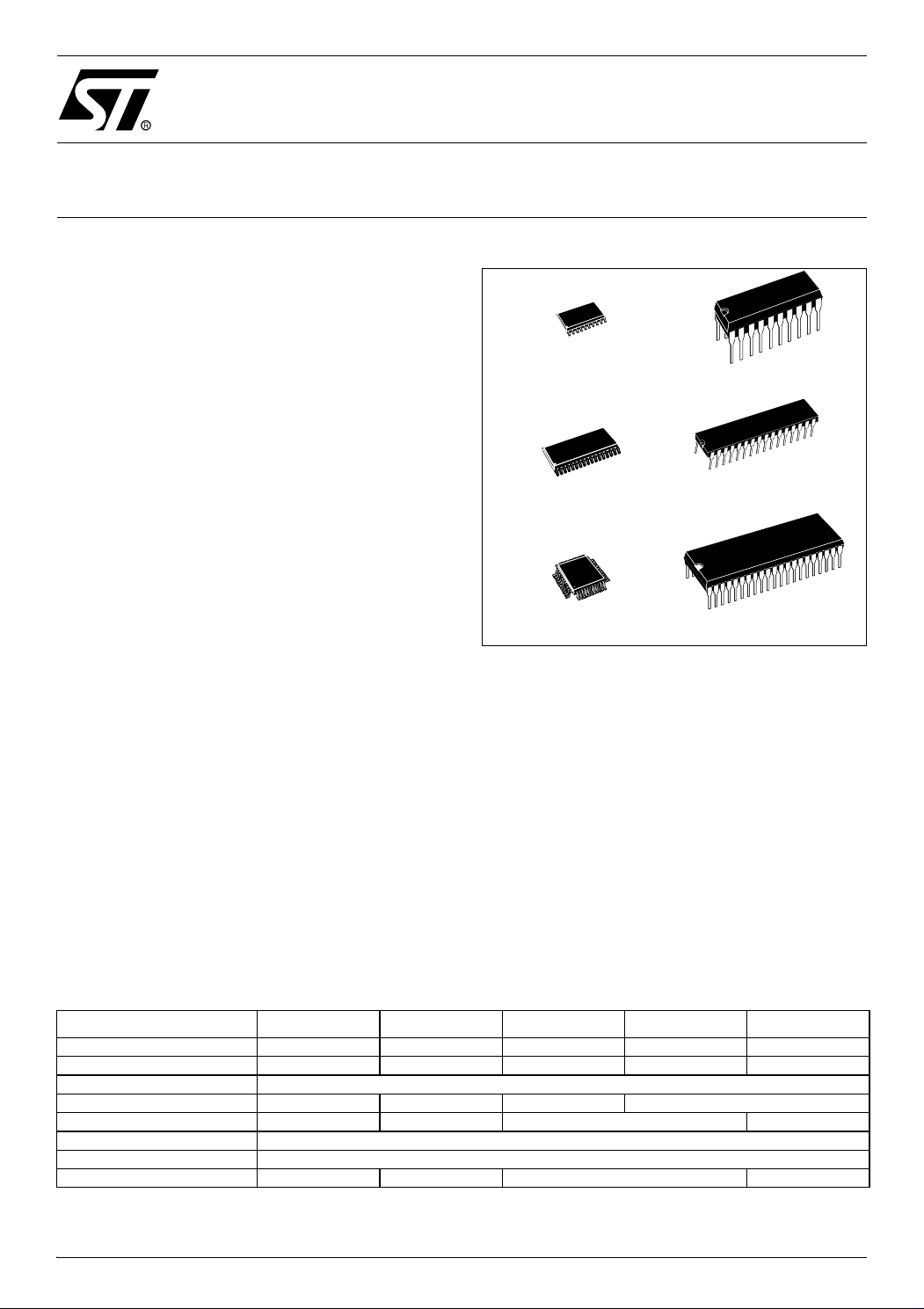
ST7262xxx
PDIP32 shrinkSO34 shrink
LQFP44 PDIP42 shrink
SO20 PDIP20
Low speed USB 8-bit MCU with 3 endpoints, Flash or
ROM memory, LVD, WDG, 10-bit ADC, 2 timers, SCI, SPI
Features
■ Memories
– 8 or 16 Kbyte Program memory
(ROM or Dual voltage FLASH)
with read-write protection
– In-Application and In-Circuit Programming for
FLASH versions
– 384 to 768 bytes RAM (128-byte stack)
■ Clock, Reset and Supply Management
– Enhanced Reset System (Power On Reset)
– Low Voltage Detector (LVD)
– Clock-out capability
– 6 or 12 MHz Oscillator (8, 4, 2, 1 MHz internal
frequencies)
– 3 Power saving modes
■ USB (Universal Serial Bus) Interface
– DMA for low speed applications compliant
with USB specification (version 2.0):
– Integrated 3.3V voltage regulator and trans-
ceivers
– Suspend and Resume operations
– 3 Endpoints
■ Up to 31 I/O Ports
– Up to 31 multifunctional bidirectional I/O lines
– Up to 12 External interrupts (3 vectors)
– 13 alternate function lines
– 8 high sink outputs
(8 mA@0.4 V/20 mA@1.3 V)
– 2 true open drain pins (N buffer 8 mA@0.4 V)
■ 3 Timers
– Configurable watchdog timer (8 to 500 ms
timeout)
– 8-bit Auto Reload Timer (ART) with 2 Input
Captures, 2 PWM outputs and External Clock
– 8-bit Time Base Unit (TBU) for generating pe-
riodic interrupts cascadable with ART
Device Summary
Features ST72623F2 ST72621K4 ST72622L2 ST72621L4 ST72621J4
Program memory - Kbytes 8 16 8 16 16
RAM (stack) - bytes 384 (128) 768 (128) 384 (128) 768 (128) 768 (128)
Peripherals USB, Watchdog, Low Voltage Detector, 8-bit Auto-Reload timer, Timebase unit, A/D Converter
Serial I/O - SPI + SCI SPI SPI + SCI
I/Os 11212331
Operating Supply 4.0V to 5.5V (Low voltage 3.0V to 5.5V ROM versions available)
Operating Temperature 0°C to +70°C
Packages PDIP20/SO20 PDIP32 SO34 PDIP42/LQFP44
■ Analog Peripheral
– 10-bit A/D Converter with up to 8 input pins.
■ 2 Communications Interfaces
– Asynchronous Serial Communication inter-
face
– Synchronous Serial Peripheral Interface
■ Instruction Set
– 8-bit data manipulation
– 63 basic instructions
– 17 main addressing modes
– 8 x 8 unsigned multiply instruction
– True bit manipulation
■ Nested interrupts
■ Development Tools
– Full hardware/software development package
June 2009 1/139
Doc ID 6996 Rev 5
1

Table of Contents
1 INTRODUCTION . . . . . . . . . . . . . . . . . . . . . . . . . . . . . . . . . . . . . . . . . . . . . . . . . . . . . . . . . . . . . . 4
2 PIN DESCRIPTION . . . . . . . . . . . . . . . . . . . . . . . . . . . . . . . . . . . . . . . . . . . . . . . . . . . . . . . . . . . . 5
2.1 PCB LAYOUT RECOMMENDATION . . . . . . . . . . . . . . . . . . . . . . . . . . . . . . . . . . . . . . . . . 10
3 REGISTER & MEMORY MAP . . . . . . . . . . . . . . . . . . . . . . . . . . . . . . . . . . . . . . . . . . . . . . . . . . . 11
4 FLASH PROGRAM MEMORY . . . . . . . . . . . . . . . . . . . . . . . . . . . . . . . . . . . . . . . . . . . . . . . . . . 14
4.1 INTRODUCTION . . . . . . . . . . . . . . . . . . . . . . . . . . . . . . . . . . . . . . . . . . . . . . . . . . . . . . . . 14
4.2 MAIN FEATURES . . . . . . . . . . . . . . . . . . . . . . . . . . . . . . . . . . . . . . . . . . . . . . . . . . . . . . . 14
4.3 STRUCTURE . . . . . . . . . . . . . . . . . . . . . . . . . . . . . . . . . . . . . . . . . . . . . . . . . . . . . . . . . . . 14
4.4 ICC INTERFACE . . . . . . . . . . . . . . . . . . . . . . . . . . . . . . . . . . . . . . . . . . . . . . . . . . . . . . . . 15
4.5 ICP (IN-CIRCUIT PROGRAMMING) . . . . . . . . . . . . . . . . . . . . . . . . . . . . . . . . . . . . . . . . . 16
4.6 IAP (IN-APPLICATION PROGRAMMING) . . . . . . . . . . . . . . . . . . . . . . . . . . . . . . . . . . . . . 16
4.7 RELATED DOCUMENTATION . . . . . . . . . . . . . . . . . . . . . . . . . . . . . . . . . . . . . . . . . . . . . 16
4.8 REGISTER DESCRIPTION . . . . . . . . . . . . . . . . . . . . . . . . . . . . . . . . . . . . . . . . . . . . . . . . 16
5 CENTRAL PROCESSING UNIT . . . . . . . . . . . . . . . . . . . . . . . . . . . . . . . . . . . . . . . . . . . . . . . . . 17
5.1 INTRODUCTION . . . . . . . . . . . . . . . . . . . . . . . . . . . . . . . . . . . . . . . . . . . . . . . . . . . . . . . . 17
5.2 MAIN FEATURES . . . . . . . . . . . . . . . . . . . . . . . . . . . . . . . . . . . . . . . . . . . . . . . . . . . . . . . 17
5.3 CPU REGISTERS . . . . . . . . . . . . . . . . . . . . . . . . . . . . . . . . . . . . . . . . . . . . . . . . . . . . . . . 17
6 CLOCKS AND RESET . . . . . . . . . . . . . . . . . . . . . . . . . . . . . . . . . . . . . . . . . . . . . . . . . . . . . . . . 20
6.1 CLOCK SYSTEM . . . . . . . . . . . . . . . . . . . . . . . . . . . . . . . . . . . . . . . . . . . . . . . . . . . . . . . . 20
6.2 RESET . . . . . . . . . . . . . . . . . . . . . . . . . . . . . . . . . . . . . . . . . . . . . . . . . . . . . . . . . . . . . . . . 21
7 INTERRUPTS . . . . . . . . . . . . . . . . . . . . . . . . . . . . . . . . . . . . . . . . . . . . . . . . . . . . . . . . . . . . . . . 24
7.1 INTRODUCTION . . . . . . . . . . . . . . . . . . . . . . . . . . . . . . . . . . . . . . . . . . . . . . . . . . . . . . . . 24
7.2 MASKING AND PROCESSING FLOW . . . . . . . . . . . . . . . . . . . . . . . . . . . . . . . . . . . . . . . 24
7.3 INTERRUPTS AND LOW POWER MODES . . . . . . . . . . . . . . . . . . . . . . . . . . . . . . . . . . . 26
7.4 CONCURRENT & NESTED MANAGEMENT . . . . . . . . . . . . . . . . . . . . . . . . . . . . . . . . . . 26
7.5 INTERRUPT REGISTER DESCRIPTION . . . . . . . . . . . . . . . . . . . . . . . . . . . . . . . . . . . . . 27
8 POWER SAVING MODES . . . . . . . . . . . . . . . . . . . . . . . . . . . . . . . . . . . . . . . . . . . . . . . . . . . . . 30
8.1 INTRODUCTION . . . . . . . . . . . . . . . . . . . . . . . . . . . . . . . . . . . . . . . . . . . . . . . . . . . . . . . . 30
8.2 WAIT MODE . . . . . . . . . . . . . . . . . . . . . . . . . . . . . . . . . . . . . . . . . . . . . . . . . . . . . . . . . . . 30
8.3 HALT MODE . . . . . . . . . . . . . . . . . . . . . . . . . . . . . . . . . . . . . . . . . . . . . . . . . . . . . . . . . . . 31
9 I/O PORTS . . . . . . . . . . . . . . . . . . . . . . . . . . . . . . . . . . . . . . . . . . . . . . . . . . . . . . . . . . . . . . . . . . 32
9.1 INTRODUCTION . . . . . . . . . . . . . . . . . . . . . . . . . . . . . . . . . . . . . . . . . . . . . . . . . . . . . . . . 32
9.2 FUNCTIONAL DESCRIPTION . . . . . . . . . . . . . . . . . . . . . . . . . . . . . . . . . . . . . . . . . . . . . . 32
9.3 MISCELLANEOUS REGISTER . . . . . . . . . . . . . . . . . . . . . . . . . . . . . . . . . . . . . . . . . . . . . 40
10 ON-CHIP PERIPHERALS . . . . . . . . . . . . . . . . . . . . . . . . . . . . . . . . . . . . . . . . . . . . . . . . . . . . . 41
10.1 WATCHDOG TIMER (WDG) . . . . . . . . . . . . . . . . . . . . . . . . . . . . . . . . . . . . . . . . . . . . . . . 41
10.2 PWM AUTO-RELOAD TIMER (ART) . . . . . . . . . . . . . . . . . . . . . . . . . . . . . . . . . . . . . . . . . 43
10.3 TIMEBASE UNIT (TBU) . . . . . . . . . . . . . . . . . . . . . . . . . . . . . . . . . . . . . . . . . . . . . . . . . . . 53
10.4 SERIAL PERIPHERAL INTERFACE (SPI) . . . . . . . . . . . . . . . . . . . . . . . . . . . . . . . . . . . . 56
10.5 SERIAL COMMUNICATIONS INTERFACE (SCI) . . . . . . . . . . . . . . . . . . . . . . . . . . . . . . . 67
10.6 USB INTERFACE (USB) . . . . . . . . . . . . . . . . . . . . . . . . . . . . . . . . . . . . . . . . . . . . . . . . . . 83
139
2/139
1
Doc ID 6996 Rev 5

Table of Contents
10.7 10-BIT A/D CONVERTER (ADC) . . . . . . . . . . . . . . . . . . . . . . . . . . . . . . . . . . . . . . . . . . . . 91
11 INSTRUCTION SET . . . . . . . . . . . . . . . . . . . . . . . . . . . . . . . . . . . . . . . . . . . . . . . . . . . . . . . . . 95
11.1 CPU ADDRESSING MODES . . . . . . . . . . . . . . . . . . . . . . . . . . . . . . . . . . . . . . . . . . . . . . . 95
11.2 INSTRUCTION GROUPS . . . . . . . . . . . . . . . . . . . . . . . . . . . . . . . . . . . . . . . . . . . . . . . . . 98
12 ELECTRICAL CHARACTERISTICS . . . . . . . . . . . . . . . . . . . . . . . . . . . . . . . . . . . . . . . . . . . . 101
12.1 PARAMETER CONDITIONS . . . . . . . . . . . . . . . . . . . . . . . . . . . . . . . . . . . . . . . . . . . . . . 101
12.2 ABSOLUTE MAXIMUM RATINGS . . . . . . . . . . . . . . . . . . . . . . . . . . . . . . . . . . . . . . . . . . 102
12.3 OPERATING CONDITIONS . . . . . . . . . . . . . . . . . . . . . . . . . . . . . . . . . . . . . . . . . . . . . . . 103
12.4 SUPPLY CURRENT CHARACTERISTICS . . . . . . . . . . . . . . . . . . . . . . . . . . . . . . . . . . . 104
12.5 CLOCK AND TIMING CHARACTERISTICS . . . . . . . . . . . . . . . . . . . . . . . . . . . . . . . . . . 105
12.6 MEMORY CHARACTERISTICS . . . . . . . . . . . . . . . . . . . . . . . . . . . . . . . . . . . . . . . . . . . 107
12.7 EMC CHARACTERISTICS . . . . . . . . . . . . . . . . . . . . . . . . . . . . . . . . . . . . . . . . . . . . . . . 108
12.8 I/O PORT PIN CHARACTERISTICS . . . . . . . . . . . . . . . . . . . . . . . . . . . . . . . . . . . . . . . . 110
12.9 CONTROL PIN CHARACTERISTICS . . . . . . . . . . . . . . . . . . . . . . . . . . . . . . . . . . . . . . . 113
12.10TIMER PERIPHERAL CHARACTERISTICS . . . . . . . . . . . . . . . . . . . . . . . . . . . . . . . . . 116
12.11COMMUNICATION INTERFACE CHARACTERISTICS . . . . . . . . . . . . . . . . . . . . . . . . 117
12.1210-BIT ADC CHARACTERISTICS . . . . . . . . . . . . . . . . . . . . . . . . . . . . . . . . . . . . . . . . . 120
13 PACKAGE CHARACTERISTICS . . . . . . . . . . . . . . . . . . . . . . . . . . . . . . . . . . . . . . . . . . . . . . 124
13.1 PACKAGE MECHANICAL DATA . . . . . . . . . . . . . . . . . . . . . . . . . . . . . . . . . . . . . . . . . . . 124
14 DEVICE CONFIGURATION AND ORDERING INFORMATION . . . . . . . . . . . . . . . . . . . . . . . 128
14.1 OPTION BYTE . . . . . . . . . . . . . . . . . . . . . . . . . . . . . . . . . . . . . . . . . . . . . . . . . . . . . . . . . 128
14.2 DEVICE ORDERING INFORMATION AND TRANSFER OF CUSTOMER CODE . . . . . 128
14.3 DEVELOPMENT TOOLS . . . . . . . . . . . . . . . . . . . . . . . . . . . . . . . . . . . . . . . . . . . . . . . . . 130
14.4 ST7 APPLICATION NOTES . . . . . . . . . . . . . . . . . . . . . . . . . . . . . . . . . . . . . . . . . . . . . . 132
15 IMPORTANT NOTES . . . . . . . . . . . . . . . . . . . . . . . . . . . . . . . . . . . . . . . . . . . . . . . . . . . . . . . 135
15.1 A/ D CONVERTER ACCURACY FOR FIRST CONVERSION . . . . . . . . . . . . . . . . . . . . 135
15.2 A/D CONVERTER CONVERSION SPEED . . . . . . . . . . . . . . . . . . . . . . . . . . . . . . . . . . . 135
15.3 SCI WRONG BREAK DURATION . . . . . . . . . . . . . . . . . . . . . . . . . . . . . . . . . . . . . . . . . . 136
15.4 UNEXPECTED RESET FETCH . . . . . . . . . . . . . . . . . . . . . . . . . . . . . . . . . . . . . . . . . . . . 136
15.5 HALT MODE POWER CONSUMPTION WITH ADC ON . . . . . . . . . . . . . . . . . . . . . . . . . 136
16 REVISION HISTORY . . . . . . . . . . . . . . . . . . . . . . . . . . . . . . . . . . . . . . . . . . . . . . . . . . . . . . . . 138
3/139
139
Doc ID 6996 Rev 5

ST7262xxx
8-BIT CORE
ALU
ADDRESS AND DATA BUS
OSCIN
OSCOUT
RESET
PORT B
USB SIE
PORT A
SCI
PORT C
SPI
PB7:0
(8 bits)
PC7:0
(8 bits)
OSCILLATOR
Internal
CLOCK
CONTROL
RAM
(384,
PA7:0
(8 bits)
V
SS
V
DD
POWER
SUPPLY
PROGRAM
(8 or 16K Bytes)
LVD
10-BIT ADC
MEMORY
WATCHDOG
USBDP
USBDM
USBVCC
PWM ART
USB DMA
V
SSA
V
DDA
PORT D
PD6:0
(7 bits)
TIME BASE UNIT
V
PP
or 768 Bytes)
1 INTRODUCTION
The ST7262 and ST72F62 devices are members
of the ST7 microcontroller family designed for USB
applications.
All devices are based on a common industrystandard 8-bit core, featuring an enhanced instruction set.
The ST7262 devices are ROM versions.
The ST72F62 versions feature dual-voltage
FLASH memory with FLASH Programming capability.
Under software control, all devices can be placed
in WAIT, SLOW, or HALT mode, reducing power
Figure 1. General Block Diagram
consumption when the application is in idle or
standby state.
The enhanced instruction set and addressing
modes of the ST7 offer both power and flexibility to
software developers, enabling the design of highly
efficient and compact application code. In addition
to standard 8-bit data management, all ST7 microcontrollers feature true bit manipulation, 8x8 unsigned multiplication and indirect addressing
modes.
4/139
1
Doc ID 6996 Rev 5

2 PIN DESCRIPTION
44 43 42 41 40 39 38 37 36 35 34
33
32
31
30
29
28
27
26
25
24
23
12 13 14 15 16 17 18
19 20 21 22
1
2
3
4
5
6
7
8
9
10
11
38
37
36
35
34
33
32
31
30
29
28
27
16
15
1
2
3
4
5
6
7
8
9
10
11
12
13
14
39
40
41
42
PD6
PD5
OSCOUT
OSCIN
IT9 / PC2
IT10 / SCK / PC3
IT11 / SS
/ PC4
IT12 / MISO / PC5
MOSI / PC6
PD1
V
PP
PD2
PD3
PD4
PC7
PD0
V
DDA
USBVCC
PB1 (HS) / RDI
PB0 (HS) / MCO
PA7 / AIN7
PA6 / AIN6
PA5 / AIN5
PA4 / AIN4
PA3 / AIN3 / IT4
PA0 / AIN0 / IT1 / USBOE
RESET
V
SSA
USBDM
USBDP
PA1 / AIN1 / IT2
PA2 / AIN2 / IT3
21
20
17
18
19
IT8 / PWM1 / PB7 (HS)
PC0
PC1
V
DD
V
SS
26
25
24
23
22
PB6 (HS) / PWM0 / IT7 / ICCDATA
PB5 (HS) / ARTIC2 / IT6 / ICCCLK
PB4 (HS) / ARTIC1 / IT5
PB3 (HS) / ARTCLK
PB2 (HS) / TDO
OSCOUT
OSCIN
IT9 / PC2
IT10 / SCK / PC3
IT11 / SS
/ PC4
IT12 / MISO / PC5
MOSI / PC6
PD1
V
PP
PC7
PD0
IT8 / PWM1 / PB7
PC0
PC1
V
DD
V
SS
ARTCLK / PB3 (HS)
IT5 / ARTIC1 / PB4 (HS)
ICCCLK / IT6 / ARTIC2 / PB5 (HS)
ICCDATA /IT7 / PWM0 / PB6 (HS)
N.C.
TDO / PB2 (HS)
PB1 (HS) / RDI
PB0 (HS) / MCO
PA7 / AIN7
PA6 / AIN6
PA5 / AIN5
PA4 / AIN4
PA3 / AIN3 / IT4
PA0 / AIN0 / IT1 / USBOE
RESET
PA1 / AIN1 / IT2
PA2 / AIN2 / IT3
V
DDA
USBVCC
V
SSA
USBDM
USBDP
PD3
PD4
Reserved*
PD6
PD5
PD2
* Pin 39 of the LQFP44 package
must be left unconnected.
Figure 2. 44-pin LQFP and 42-Pin SDIP Package Pinouts
ST7262xxx
Doc ID 6996 Rev 5
5/139

ST7262xxx
28
27
26
25
24
23
22
21
20
19
18
29
30
31
32
PC4 / SS / INT11
PC5 / MISO / IT12
PA4 / AIN4
PA3 / AIN3 / IT4
PA2 / AIN2 / IT3
PA1 / AIN1 / IT2
PA0 / AIN0 / IT1 / USBOE
V
SSA
USBDM
USBVCC
V
DDA
V
PP
RESET
PC6 / MOSI
USBDP
PC7
16
15
1
2
3
4
5
6
7
8
9
10
11
12
13
14
IT10 / SCK / PC3
IT9 / PC2
AIN7 / PA7
MCO / PB0 (HS)
RDI / PB1 (HS)
TDO / PB2 (HS)
ARTCLK / PB3 (HS)
IT5 / ARTIC1 / PB4 (HS)
ICCCLK / IT6 /ARTIC2 / PB5 (HS)
IT8 / PWM1 / PB7 (HS)
V
DD
V
SS
OSCOUT
OSCIN
ICCDATA / IT7 / PWM0 / PB6 (HS)
PA5 / AIN5
AIN6 / PA6
33
34
17
28
27
26
25
24
23
22
21
20
19
18
17
16
15
1
2
3
4
5
6
7
8
9
10
11
12
13
14
29
30
31
32
IT10 / SCK / PC3
IT9 / PC2
AIN7 / PA7
MCO / PB0 (HS)
RDI / PB1 (HS)
TDO / PB2 (HS)
ARTCLK / PB3 (HS)
IT5 / ARTIC1 / PB4 (HS)
ICCCLK / IT6 / ARTIC2 / PB5 (HS)
IT8 / PWM1 / PB7 (HS)
V
DD
V
SS
OSCOUT
OSCIN
ICCDATA / IT7 / PWM0 / PB6 (HS)
AIN6 / PA6
PC4 / SS
/ INT11
PC5 / MISO / IT12
PA4 / AIN4
PA3 / AIN3 / IT4
PA2 / AIN2 / IT3
PA1 / AIN1 / IT2
PA0 / AIN0 / IT1 / USBOE
V
SSA
USBDM
USBVCC
V
DDA
V
PP
RESET
PC6 / MOSI
USBDP
PA5 / AIN5
PC1
PIN DESCRIPTION (Cont’d)
Figure 3. 34-Pin SO and 32-Pin SDIP Package Pinouts
6/139
Doc ID 6996 Rev 5

Figure 4. 20-pin SO20 Package Pinout
14
13
12
11
15
16
17
18
OSCIN
OSCOUT
PB7 (HS) / PWM1 / IT8
PB6 (HS) / PWM0 / IT7/ ICCDATA
USBVCC
V
DD
V
PP
USBDP
1
2
3
4
5
6
7
8
9
10
IT3 / AIN2 / PA2
PB0 (HS) / MCO
PB1 (HS)
PB2 (HS)
PB3 (HS) / ARTCLK
PB4 (HS) / ARTIC1 / IT5
RESET
IT2 / AIN1 / PA1
19
20
USBOE/ IT1 / AIN0/ PA0
V
SS
USBDM
PB5 (HS) / ARTIC2 / IT6 / ICCCLK
14
13
12
11
15
16
17
18
OSCIN
OSCOUT
PB7 (HS) / PWM1 / IT8
PB6 (HS) / PWM0 / IT7/ICCDATA
USBVCC
V
DD
V
PP
USBDP
1
2
3
4
5
6
7
8
9
10
IT5 / ARTIC1 / PB4 (HS)
MCO / PB0 (HS)
PB1 (HS)
PB2 (HS)
RESET
IT2 / AIN1/ PA1
19
20
USBOE / IT1 / AIN0 / PA0
V
SS
USBDM
PB5 (HS) / ARTIC2 / IT6 / ICCCLK
IT3 / AIN2 / PA2
ARTCLK / PB3 (HS)
Figure 5. 20-pin DIP20 Package Pinout
ST7262xxx
Doc ID 6996 Rev 5
7/139

ST7262xxx
PIN DESCRIPTION (Cont’d)
Legend / Abbreviations:
Type: I = Input, O = Output, S = Supply
Input level: A = Dedicated analog input
Input level: C = CMOS 0.3V
= CMOS 0.3VDD/0.7VDD with input trigger
C
T
Output level: HS = High Sink (on N-buffer only)
Port configuration capabilities:
– Input:float = floating, wpu = weak pull-up, int = interrupt (\ =falling edge, / =rising edge
ana = analog
– Output: OD = open drain, T = true open drain (N buffer 8mA@0.4 V), PP = push-pull
Table 1. Device Pin Description
/0.7VDD,
DD
),
Pin n°
DIP42
LQFP44
SO34
SO20
DIP32
Pin Name
DIP20
Level Port / Control
Input Output
Type
Input
Output
float
wpu
int
ana
OD
Main
Function
(after
reset)
PP
Alternate Function
FLASH programming voltage
1 6 29 28 9 14 V
PP
Sx
(12V), must be tied low in user
mode.
27----PD1 I/OC
38----PD0 I/OC
4931---PC7 I/OC
5 103230 - - PC6/MOSI I/OC
T
T
T
T
xxPort D1
xxPort D0
xxPort C7
xxPort C6
SPI Master Out /
Slave In
SPI Master In /
6 11 33 31 - - PC5/MISO/IT12 I/O C
T
xx xPort C5
Slave Out 1) /
Interrupt 12 input
SPI Slave Select
7 123432 - - PC4/SS
/IT11 I/O C
T
xx xPort C4
(active low) 1)/
Interrupt 11 input
8 13 1 1 - - PC3/SCK/IT10 I/O C
9142 2 - -PC2/IT9 I/OC
10 15 3 3 11 16 OSCIN
T
T
xx xPort C3
xx xPort C2 Interrupt 9 input
These pins are used connect an
SPI Serial Clock
Interrupt 10 input
external clock source to the on-
11 16 4 4 12 17 OSCOUT
12 17 5 5 4 9 V
13 18 6 6 8 13 V
SS
DD
14 19 7 - - - PC1 I/O C
1520----PC0 I/OC
S Digital Ground Voltage
S
T
T
PB7/PWM1/IT8/
16 21 8 7 13 18
RX_SEZ/DA-
I/O C
T
TAOUT/DA9
xTPort C1
xTPort C0
HS x \ x Port B7
chip main oscillator.
Digital Main Power Supply Voltage
ART PWM output 1/
Interrupt 8 input
17 - - N.C. Not Connected
1)
1)
/
8/139
Doc ID 6996 Rev 5

ST7262xxx
Pin n°
DIP42
LQFP44
SO34
SO20
DIP32
Pin Name
DIP20
Level Port / Control
Input Output
Type
Input
Output
float
wpu
int
ana
OD
Main
Function
(after
reset)
PP
Alternate Function
ART PWM output 0/
18 22 9 8 14 19
PB6/PWM0/IT7/
ICCDATA
I/O C
HS x \ x Port B6
T
Interrupt 7 input/InCircuit Communication Data
ART Input Capture 2/
19 23 10 9 15 20
PB5/ARTIC2/IT6/
ICCCLK
I/O C
HS x / x Port B5
T
Interrupt 6 input/
In-Circuit Communication Clock
20 24 11 10 16 1 PB4/ARTIC1/IT5 I/O C
21 25 12 11 17 2 PB3/ARTCLK I/O C
22 26 13 12 18 3 PB2/TDO I/O C
HS x / x Port B4
T
HS x x Port B3 ART Clock input
T
HS x x Port B2
T
23 27 14 13 19 4 PB1/RDI I/O CTHS x x Port B1
ART Input Capture
1/Interrupt 5 input
SCI Transmit Data
1)
Output
SCI Receive Data
1)
Input
24 28 15 14 20 5 PB0/MCO I/O CTHS x x Port B0 CPU clock output
25 29 16 15 - - PA7/AIN7 I/O C
26 30 17 16 - - PA6/AIN6 I/O C
27 31 18 17 - - PA5/AIN5 I/O C
28 32 19 18 - - PA4/AIN4 I/O C
29 33 20 19 - - PA3/AIN3/IT4 I/O C
30 34 21 20 1 6 PA2/AIN2/IT3 I/O C
31 35 22 21 2 7 PA1/AIN1/IT2 I/O C
32 36 23 22 3 8
33 37 30 29 10 15 RESET
34 38 24 23 - - V
PA0/AIN0/IT1/
USBOE
SSA
I/O C
I/O C
S
T
T
T
T
T
T
T
T
xxxPort A7 ADC Analog Input 7
xxxPort A6 ADC Analog Input 6
xxxPort A5 ADC Analog Input 5
xxxPort A4 ADC Analog Input 4
x\xxPort A3
x\xxPort A2
x\xxPort A1
ADC Analog Input 3/
Interrupt 4 input
ADC Analog Input 2/
Interrupt 3 input
ADC Analog Input 1/
Interrupt 2 input
ADC Analog Input 0/
x\xxPort A0
Interrupt 1 input/
USB Output Enable
Top priority non maskable interrupt (active low)
Analog Ground Voltage, must
be connected externally to V
SS
35 39 25 24 5 10 USBDM I/O USB bidirectional data (data -)
36 40 26 25 6 11 USBDP I/O USB bidirectional data (data +)
37 41 27 26 7 12 USBVCC S USB power supply 3.3V output
Analog Power Supply Voltage,
38 42 28 27 - - V
DDA
S
must be connected externally to
.
V
DD
39-----Reserved Must be left unconnected.
401----PD6 I/OC
412----PD5 I/OC
423----PD4 I/OC
T
T
T
xxPort D6
xxPort D5
xxPort D4
.
Doc ID 6996 Rev 5
9/139

ST7262xxx
14
13
12
11
15
16
17
18
USBVCC
USBDP
1
2
3
4
5
6
7
8
9
10
19
20
USBDM
USB Connector
Ground
Ground
ST7262
1.5KOhm pull-up resistor
Pin n°
Pin Name
DIP42
LQFP44
SO34
SO20
DIP32
DIP20
434----PD3 I/OC
445----PD2 I/OC
Level Port / Control
Input Output
Type
Input
Output
T
T
wpu
float
xxPort D3
xxPort D2
int
ana
OD
Main
Function
(after
reset)
PP
Note 1: Peripheral not present on all devices. Refer to “Device Summary” on page 1.
2.1 PCB LAYOUT RECOMMENDATION
In the case of DIP20 devices the user should layout the PCB so that the DIP20 ST7262 device and
the USB connector are centered on the same axis
ensuring that the D- and D+ lines are of equal
length. Refer to Figure 6
Figure 6. Recommended PCB Layout for USB Interface with DIP20 package
Alternate Function
10/139
Doc ID 6996 Rev 5

3 REGISTER & MEMORY MAP
0000h
Program Memory
Interrupt & Reset Vectors
HW Registers
BFFFh
0040h
003Fh
(see Table 2)
C000h
FFDFh
FFE0h
FFFFh
(see Table 6)
0340h
Reserved
033Fh
Short Addressing
RAM (zero page)
or Stack
017Fh
0040h
00FFh
768 Bytes RAM
E000h
8 KBytes
(128 Bytes)
16 KBytes
384 Bytes RAM
64 Bytes
01BFh
16-bit Addressing
RAM
Short Addressing
RAM (zero page)
017Fh
0040h
00FFh
448 Bytes
033Fh
16-bit Addressing
RAM
16-bit Addressing
RAM
or Stack
(128 Bytes)
16-bit Addressing
RAM
192 Bytes
192 Bytes
ST7262xxx
As shown in the Figure 7, the MCU is capable of
addressing 64K bytes of memories and I/O registers.
The available memory locations consist of 64
bytes of register locations, 768 bytes of RAM and
up to 16 Kbytes of user program memory. The
RAM space includes up to 128 bytes for the stack
from 0100h to 017Fh.
The highest address bytes contain the user reset
and interrupt vectors.
Figure 7. Memory Map
IMPORTANT: Memory locations marked as “Re-
served” must never be accessed. Accessing a reserved area can have unpredictable effects on the
device.
Doc ID 6996 Rev 5
11/139

ST7262xxx
Table 2. Hardware Register Map
Address Block
0000h
0001h
0002h
0003h
0004h
0005h
0006h
0007h
Port A
Port B
Port C
Port D
Register
Label
PADR
PADDR
PBDR
PBDDR
PCDR
PCDDR
PDDR
PDDDR
Register Name
Port A Data Register
Port A Data Direction Register
Port B Data Register
Port B Data Direction Register
Port C Data Register
Port C Data Direction Register
Port D Data Register
Port D Data Direction Register
Reset
Status
1)
00h
00h
1)
00h
00h
1)
00h
00h
1)
00h
00h
0008h ITRFRE1 Interrupt Register 1 00h R/W
0009h MISC Miscellaneous Register 00h R/W
000Ah
000Bh
000Ch
ADC
ADCDRMSB
ADCDRLSB
ADCCSR
ADC Data Register (bit 9:2)
ADC Data Register (bit 1:0)
ADC Control Status Register
00h
00h
00h
000Dh WDG WDGCR Watchdog Control Register 7Fh R/W
000Eh
0010h
0011h
0012h
0013h
SPI
SPIDR
SPICR
SPICSR
SPI Data I/O Register
SPI Control Register
SPI Control Status Register
Reserved Area (3 Bytes)
xxh
0xh
00h
Remarks
2)
R/W
2)
R/W
2)
R/W
2)
R/W
2)
R/W
2)
R/W
2)
R/W
2)
R/W
Read Only
Read Only
R/W
R/W
R/W
Read Only
0014h
0015h
0016h
0017h
0018h
0019h
001Ah
001Bh
001Ch
001Dh
001Eh
001Fh
0020h
0021h
0022h
0023h
0024h
PWM ART
SCI
PWMDCR1
PWMDCR0
PWMCR
ARTCSR
ARTCAR
ARTARR
ARTICCSR
ARTICR1
ARTICR2
SCIERPR
SCIETPR
SCISR
SCIDR
SCIBRR
SCICR1
SCICR2
PWM AR Timer Duty Cycle Register 1
PWM AR Timer Duty Cycle Register 0
PWM AR Timer Control Register
Auto-Reload Timer Control/Status Register
Auto-Reload Timer Counter Access Register
Auto-Reload Timer Auto-Reload Register
ART Input Capture Control/Status Register
ART Input Capture Register 1
ART Input Capture Register 2
SCI Extended Receive Prescaler register
SCI Extended Transmit Prescaler Register
Reserved Area
SCI Status register
SCI Data register
SCI Baud Rate Register
SCI Control Register 1
SCI Control Register 2
00h
00h
00h
00h
00h
00h
00h
00h
00h
00h
00h
--
C0h
xxh
00h
x000 0000b
00h
R/W
R/W
R/W
R/W
R/W
R/W
R/W
Read Only
Read Only
R/W
R/W
Read Only
R/W
R/W
R/W
R/W
12/139
Doc ID 6996 Rev 5

ST7262xxx
Address Block
0025h
0026h
0027h
0028h
0029h
002Ah
002Bh
002Ch
002Dh
002Eh
002Fh
0030h
0031h
0032h
to
0035h
0036h
0037h
0038h FLASH FCSR Flash Control/Status Register 00h R/W
0039h ITRFRE2 Interrupt Register 2 00h R/W
003Ah
to
003Fh
USB
TBU
Register
Label
USBPIDR
USBDMAR
USBIDR
USBISTR
USBIMR
USBCTLR
USBDADDR
USBEP0RA
USBEP0RB
USBEP1RA
USBEP1RB
USBEP2RA
USBEP2RB
TBUCV
TBUCSR
Register Name
USB PID Register
USB DMA Address register
USB Interrupt/DMA Register
USB Interrupt Status Register
USB Interrupt Mask Register
USB Control Register
USB Device Address Register
USB Endpoint 0 Register A
USB Endpoint 0 Register B
USB Endpoint 1 Register A
USB Endpoint 1 Register B
USB Endpoint 2 Register A
USB Endpoint 2 Register B
Reserved Area (4 Bytes)
TBU Counter Value Register
TBU Control/Status Register
Reserved Area (6 Bytes)
Reset
Status
x0h
xxh
x0h
00h
00h
06h
00h
0000 xxxxb
80h
0000 xxxxb
0000 xxxxb
0000 xxxxb
0000 xxxxb
00h
00h
Remarks
Read Only
R/W
R/W
R/W
R/W
R/W
R/W
R/W
R/W
R/W
R/W
R/W
R/W
R/W
R/W
Legend: x=undefined, R/W=read/write
Notes:
1. The contents of the I/O port DR registers are readable only in output configuration. In input configuration, the values of the I/O pins are returned instead of the DR register contents.
2. The bits associated with unavailable pins must always be kept at their reset value.
Doc ID 6996 Rev 5
13/139

ST7262xxx
4 Kbytes
4 Kbytes
2Kbytes
SECTOR 1
SECTOR 0
16 Kbytes
SECTOR 2
8K 16K 32K 60K
FLASH
FFFFh
EFFFh
DFFFh
3FFFh
7FFFh
1000h
24 Kbytes
MEMORY SIZE
8 Kbytes 40 Kbytes
52 Kbytes
9FFFh
BFFFh
D7FFh
4K 10K 24K 48K
4 FLASH PROGRAM MEMORY
4.1 INTRODUCTION
The ST7 dual voltage High Density Flash
(HDFlash) is a non-volatile memory that can be
electrically erased as a single block or by individual sectors and programmed on a Byte-by-Byte basis using an external V
supply.
PP
The HDFlash devices can be programmed and
erased off-board (plugged in a programming tool)
or on-board using ICP (In-Circuit Programming) or
IAP (In-Application Programming).
The array matrix organisation allows each sector
to be erased and reprogrammed without affecting
other sectors.
4.2 MAIN FEATURES
■ 3 Flash programming modes:
– Insertion in a programming tool. In this mode,
all sectors including option bytes can be programmed or erased.
– ICP (In-Circuit Programming). In this mode, all
sectors including option bytes can be programmed or erased without removing the device from the application board.
– IAP (In-Application Programming) In this
mode, all sectors except Sector 0, can be programmed or erased without removing the device from the application board and while the
application is running.
■ ICT (In-Circuit Testing) for downloading and
executing user application test patterns in RAM
■ Read-out protection
■ Register Access Security System (RASS) to
prevent accidental programming or erasing
4.3 STRUCTURE
The Flash memory is organised in sectors and can
be used for both code and data storage.
Depending on the overall Flash memory size in the
microcontroller device, there are up to three user
sectors (see Table 3). Each of these sectors can
be erased independently to avoid unnecessary
erasing of the whole Flash memory when only a
partial erasing is required.
The first two sectors have a fixed size of 4 Kbytes
(see Figure 8). They are mapped in the upper part
of the ST7 addressing space so the reset and interrupt vectors are located in Sector 0 (F000hFFFFh).
Table 3. Sectors available in Flash devices
Flash Size (bytes) Available Sectors
4K Sector 0
8K Sectors 0,1
> 8K Sectors 0,1, 2
4.3.1 Read-out Protection
Read-out protection, when selected, provides a
protection against Program Memory content extraction and against write access to Flash memory. Even if no protection can be considered as totally unbreakable, the feature provides a very high
level of protection for a general purpose microcontroller.
In Flash devices, this protection is removed by reprogramming the option. In this case, the entire
program memory is first automatically erased and
the device can be reprogrammed.
Read-out protection selection depends on the device type:
– In Flash devices it is enabled and removed
through the FMP_R bit in the option byte.
– In ROM devices it is enabled by mask option
specified in the Option List.
Figure 8. Memory Map and Sector Address
14/139
Doc ID 6996 Rev 5

FLASH PROGRAM MEMORY (Cont’d)
ICC CONNECTOR
ICCDATA
ICCCLK
RESET
V
DD
HE10 CONNECTOR TYPE
APPLICATION
POWER SUPPLY
1
246810
975 3
PROGRAMMING TOOL
ICC CONNECTOR
APPLICATION BOARD
ICC Cable
(See Note 3)
10kΩ
V
SS
ICCSEL/VPP
ST7
C
L2
C
L1
OSC1
OSC2
OPTIONAL
See Note 1
See Note 2
APPLICATION
RESET SOURCE
APPLICATION
I/O
(See Note 4)
ST7262xxx
4.4 ICC INTERFACE
ICC (In-Circuit Communication) needs a minimum
of four and up to six pins to be connected to the
programming tool (see Figure 9). These pins are:
– RESET
–V
: device reset
: device power supply ground
SS
Figure 9. Typical ICC Interface
– ICCCLK: ICC output serial clock pin
– ICCDATA: ICC input/output serial data pin
– ICCSEL/V
: programming voltage
PP
– OSC1(or OSCIN): main clock input for exter-
nal source (optional)
: application board power supply (see Fig-
–V
DD
ure 9, Note 3)
Notes:
1. If the ICCCLK or ICCDATA pins are only used
as outputs in the application, no signal isolation is
necessary. As soon as the Programming Tool is
plugged to the board, even if an ICC session is not
in progress, the ICCCLK and ICCDATA pins are
not available for the application. If they are used as
inputs by the application, isolation such as a serial
resistor has to implemented in case another device forces the signal. Refer to the Programming
Tool documentation for recommended resistor values.
2. During the ICC session, the programming tool
must control the RESET
flicts between the programming tool and the application reset circuit if it drives more than 5mA at
high level (push pull output or pull-up resistor<1K).
A schottky diode can be used to isolate the application RESET circuit in this case. When using a
classical RC network with R > 1K or a reset man-
pin. This can lead to con-
Doc ID 6996 Rev 5
agement IC with open drain output and pull-up
resistor > 1K, no additional components are needed. In all cases the user must ensure that no external reset is generated by the application during the
ICC session.
3. The use of Pin 7 of the ICC connector depends
on the Programming Tool architecture. This pin
must be connected when using most ST Programming Tools (it is used to monitor the application
power supply). Please refer to the Programming
Tool manual.
4. Pin 9 has to be connected to the OSC1 or OSCIN pin of the ST7 when the clock is not available
in the application or if the selected clock option is
not programmed in the option byte. ST7 devices
with multioscillator capability need to have OSC2
grounded in this case.
15/139

ST7262xxx
FLASH PROGRAM MEMORY (Cont’d)
4.5 ICP (IN-CIRCUIT PROGRAMMING)
To perform ICP the microcontroller must be
switched to ICC (In-Circuit Communication) mode
by an external controller or programming tool.
Depending on the ICP code downloaded in RAM,
Flash memory programming can be fully customized (number of bytes to program, program locations, or selection serial communication interface
for downloading).
When using an STMicroelectronics or third-party
programming tool that supports ICP and the specific microcontroller device, the user needs only to
implement the ICP hardware interface on the application board (see Figure 9). For more details on
the pin locations, refer to the device pinout description.
4.6 IAP (IN-APPLICATION PROGRAMMING)
This mode uses a BootLoader program previously
stored in Sector 0 by the user (in ICP mode or by
plugging the device in a programming tool).
This mode is fully controlled by user software. This
allows it to be adapted to the user application, (user-defined strategy for entering programming
mode, choice of communications protocol used to
fetch the data to be stored, etc.). For example, it is
possible to download code from the SPI, SCI or
other type of serial interface and program it in the
Flash. IAP mode can be used to program any of
the Flash sectors except Sector 0, which is write/
erase protected to allow recovery in case errors
occur during the programming operation.
4.7 RELATED DOCUMENTATION
For details on Flash programming and ICC protocol, refer to the ST7 Flash Programming Refer-
ence Manual and to the ST7 ICC Protocol Reference Manual
.
4.8 REGISTER DESCRIPTION
FLASH CONTROL/STATUS REGISTER (FCSR)
Read/Write
Reset Value: 0000 0000 (00h)
70
00000000
This register is reserved for use by Programming
Tool software. It controls the Flash programming
and erasing operations.
16/139
Doc ID 6996 Rev 5

5 CENTRAL PROCESSING UNIT
ACCUMULATOR
X INDEX REGISTER
Y INDEX REGISTER
STACK POINTER
CONDITION CODE REGISTER
PROGRAM COUNTER
70
1C1I1HI0NZ
RESET VALUE = RESET VECTOR @ FFFEh-FFFFh
70
70
70
0
7
15 8
PCH
PCL
15
8
70
RESET VALUE = STACK HIGHER ADDRESS
RESET VALUE =
1X11X1XX
RESET VALUE = XXh
RESET VALUE = XXh
RESET VALUE = XXh
X = Undefined Value
ST7262xxx
5.1 INTRODUCTION
This CPU has a full 8-bit architecture and contains
six internal registers allowing efficient 8-bit data
manipulation.
5.2 MAIN FEATURES
■ Enable executing 63 basic instructions
■ Fast 8-bit by 8-bit multiply
■ 17 main addressing modes (with indirect
addressing mode)
■ Two 8-bit index registers
■ 16-bit stack pointer
■ Low power HALT and WAIT modes
■ Priority maskable hardware interrupts
■ Non-maskable software/hardware interrupts
Figure 10. CPU Registers
5.3 CPU REGISTERS
The 6 CPU registers shown in Figure 10 are not
present in the memory mapping and are accessed
by specific instructions.
Accumulator (A)
The Accumulator is an 8-bit general purpose register used to hold operands and the results of the
arithmetic and logic calculations and to manipulate
data.
Index Registers (X and Y)
These 8-bit registers are used to create effective
addresses or as temporary storage areas for data
manipulation. (The Cross-Assembler generates a
precede instruction (PRE) to indicate that the following instruction refers to the Y register.)
The Y register is not affected by the interrupt automatic procedures.
Program Counter (PC)
The program counter is a 16-bit register containing
the address of the next instruction to be executed
by the CPU. It is made of two 8-bit registers PCL
(Program Counter Low which is the LSB) and PCH
(Program Counter High which is the MSB).
Doc ID 6996 Rev 5
17/139

ST7262xxx
CENTRAL PROCESSING UNIT (Cont’d)
Condition Code Register (CC)
Read/Write
Reset Value: 111x1xxx
70
11I1HI0NZ
C
The 8-bit Condition Code register contains the interrupt masks and four flags representative of the
result of the instruction just executed. This register
can also be handled by the PUSH and POP instructions.
These bits can be individually tested and/or controlled by specific instructions.
Arithmetic Management Bits
Bit 4 = H Half carry.
This bit is set by hardware when a carry occurs be-
tween bits 3 and 4 of the ALU during an ADD or
ADC instructions. It is reset by hardware during
the same instructions.
0: No half carry has occurred.
1: A half carry has occurred.
This bit is tested using the JRH or JRNH instruction. The H bit is useful in BCD arithmetic subroutines.
Bit 2 = N Negative.
This bit is set and cleared by hardware. It is repre-
sentative of the result sign of the last arithmetic,
logical or data manipulation. It’s a copy of the re-
th
sult 7
bit.
0: The result of the last operation is positive or null.
1: The result of the last operation is negative
(i.e. the most significant bit is a logic 1).
This bit is accessed by the JRMI and JRPL instructions.
Bit 1 = Z Zero.
This bit is set and cleared by hardware. This bit indicates that the result of the last arithmetic, logical
or data manipulation is zero.
0: The result of the last operation is different from
zero.
1: The result of the last operation is zero.
This bit is accessed by the JREQ and JRNE test
instructions.
Bit 0 = C Carry/borrow.
This bit is set and cleared by hardware and software. It indicates an overflow or an underflow has
occurred during the last arithmetic operation.
0: No overflow or underflow has occurred.
1: An overflow or underflow has occurred.
This bit is driven by the SCF and RCF instructions
and tested by the JRC and JRNC instructions. It is
also affected by the “bit test and branch”, shift and
rotate instructions.
Interrupt Management Bits
Bit 5,3 = I1, I0 Interrupt
The combination of the I1 and I0 bits gives the cur-
rent interrupt software priority.
Interrupt Software Priority I1 I0
Level 0 (main) 1 0
Level 1 0 1
Level 2 0 0
Level 3 (= interrupt disable) 1 1
These two bits are set/cleared by hardware when
entering in interrupt. The loaded value is given by
the corresponding bits in the interrupt software priority registers (IxSPR). They can be also set/
cleared by software with the RIM, SIM, IRET,
HALT, WFI and PUSH/POP instructions.
See the interrupt management chapter for more
details.
18/139
Doc ID 6996 Rev 5

CPU REGISTERS (Cont’d)
PCH
PCL
SP
PCH
PCL
SP
PCL
PCH
X
A
CC
PCH
PCL
SP
PCL
PCH
X
A
CC
PCH
PCL
SP
PCL
PCH
X
A
CC
PCH
PCL
SP
SP
Y
CALL
Subroutine
Interrupt
Event
PUSH Y POP Y IRET
RET
or RSP
@ 017Fh
@ 0100h
Stack Higher Address = 017Fh
Stack Lower Address =
0100h
STACK POINTER (SP)
Read/Write
Reset Value: 017Fh
15 8
00000001
Note: When the lower limit is exceeded, the Stack
Pointer wraps around to the stack upper limit, without indicating the stack overflow. The previously
stored information is then overwritten and therefore lost. The stack also wraps in case of an underflow.
The stack is used to save the return address during a subroutine call and the CPU context during
70
1 SP6 SP5 SP4 SP3 SP2 SP1 SP0
an interrupt. The user may also directly manipulate
the stack by means of the PUSH and POP instructions. In the case of an interrupt, the PCL is stored
at the first location pointed to by the SP. Then the
other registers are stored in the next locations as
shown in Figure 11.
The Stack Pointer is a 16-bit register which is always pointing to the next free location in the stack.
It is then decremented after data has been pushed
onto the stack and incremented before data is
popped from the stack (see Figure 11).
Since the stack is 128 bytes deep, the 9 most significant bits are forced by hardware. Following an
– When an interrupt is received, the SP is decre-
mented and the context is pushed on the stack.
– On return from interrupt, the SP is incremented
and the context is popped from the stack.
A subroutine call occupies two locations and an interrupt five locations in the stack area.
MCU Reset, or after a Reset Stack Pointer instruction (RSP), the Stack Pointer contains its reset value (the SP6 to SP0 bits are set) which is the stack
higher address.
The least significant byte of the Stack Pointer
(called S) can be directly accessed by a LD instruction.
ST7262xxx
Figure 11. Stack Manipulation Example
Doc ID 6996 Rev 5
19/139

ST7262xxx
OSCIN
OSCOUT
EXTERNAL
CLOCK
NC
OSCIN
OSCOUT
C
OSCIN
C
OSCOUT
6 CLOCKS AND RESET
6.1 CLOCK SYSTEM
6.1.1 General Description
The MCU accepts either a Crystal or Ceramic resonator, or an external clock signal to drive the internal oscillator. The internal clock (f
rived from the external oscillator frequency (f
CPU
) is de-
OSC
by dividing by 3 and multiplying by 2. By setting the
OSC12/6 bit in the option byte, a 12 MHz external
clock can be used giving an internal frequency of 8
MHz while maintaining a 6 MHz clock for USB (refer to Figure 14).
The internal clock signal (f
) consists of a
CPU
square wave with a duty cycle of 50%.
It is further divided by 1, 2, 4 or 8 depending on the
Slow Mode Selection bits in the Miscellaneous
register (SMS[1:0])
The internal oscillator is designed to operate with
an AT-cut parallel resonant quartz or ceramic resonator in the frequency range specified for f
osc
The circuit shown in Figure 13 is recommended
when using a crystal, and Table 4 lists the recommended capacitors. The crystal and associated
components should be mounted as close as possible to the input pins in order to minimize output
distortion and start-up stabilization time.
6.1.2 External Clock input
An external clock may be applied to the OSCIN input with the OSCOUT pin not connected, as
shown on Figure 12. The t
does not apply when using an external clock input.
),
specifications
OXOV
The equivalent specification of the external clock
source should be used instead of t
OXOV
trical Characteristics).
6.1.3 Clock Output Pin (MCO)
The internal clock (f
) can be output on Port B0
CPU
by setting the MCO bit in the Miscellaneous register.
Figure 12. External Clock Source Connections
.
(see Elec-
Table 4. Recommended Values for 12 MHz
Crystal Resonator
R
SMAX
C
OSCIN
C
OSCOUT
R
P
Note: R
crystal (see crystal specification).
SMAX
20 Ω 25 Ω 70 Ω
56pF 47pF 22pF
56pF 47pF 22pF
1-10 MΩ 1-10 MΩ 1-10 MΩ
is the equivalent serial resistor of the
Note: When a crystal is used, and to not overstress the crystal, ST recommends to add a serial
resistor on the OSCOUT pin to limit the drive level
in accordance with the crystal manufacturer’s
specification. Please also refer to Section 12.5.4.
20/139
Figure 13. Crystal/Ceramic Resonator
Doc ID 6996 Rev 5

Figure 14. Clock block diagram
to CPU and
f
CPU
8/4/2/1 MHz
6 MHz (USB)
12 or
peripherals
%2
0
1
OSC12/6
6 MHz
Crystal
x2
Slow
Mode
%
SMS[1:0]
1/2/4/8
%3
(or 4/2/1/0.5 MHz)
MCO pin
LOW VOLTAGE
V
DD
FROM
WATCHDOG
RESET
RESET
INTERNAL
RESET
RESET
6.2 RESET
ST7262xxx
The Reset procedure is used to provide an orderly
software start-up or to exit low power modes.
Three reset modes are provided: a low voltage reset, a watchdog reset and an external reset at the
RESET
pin.
A reset causes the reset vector to be fetched from
addresses FFFEh and FFFFh in order to be loaded
into the PC and with program execution starting
from this point.
An internal circuitry provides a 514 CPU clock cycle delay from the time that the oscillator becomes
active.
Caution: When the ST7 is unprogrammed or fully
erased, the Flash is blank and the RESET vector
is not programmed. For this reason, it is recommended to keep the RESET pin in low state until
programming mode is entered, in order to avoid
unwanted behaviour.
6.2.1 Low Voltage Reset
Low voltage reset circuitry generates a reset when
is:
V
DD
■ below V
■ below V
During low voltage reset, the RESET
when VDD is rising,
IT+
when VDD is falling.
IT-
pin is held low,
thus permitting the MCU to reset other devices.
Notes:
The Low Voltage Detector can be disabled by setting the LVD bit of the Option byte.
It is recommended to make sure that the V
voltage rises monotonously when the device is exiting from Reset, to ensure the application functions
properly.
6.2.2 Watchdog Reset
When a watchdog reset occurs, the RESET
pulled low permitting the MCU to reset other devices as when low voltage reset (Figure 15).
6.2.3 External Reset
The external reset is an active low input signal applied to the RESET
pin of the MCU.
As shown in Figure 18, the RESET
stay low for a minimum of one and a half CPU
clock cycles.
An internal Schmitt trigger at the RESET
vided to improve noise immunity.
Figure 15. Low Voltage Reset functional Diagram
Doc ID 6996 Rev 5
supply
DD
pin is
signal must
pin is pro-
21/139

ST7262xxx
RESET
V
DD
V
IT+
V
IT-
V
DD
Addresses
$FFFE
Temporization
V
IT+
(514 CPU clock cycles)
V
DD
OSCIN
f
CPU
FFFF
FFFE
PC
RESET
t
DDR
t
OXOV
514 CPU
CLOCK
CYCLES
DELAY
Figure 16. Low Voltage Reset Signal Output
Note: Typical hysteresis (V
IT+-VIT-
) of 250 mV is expected.
Figure 17. Temporization Timing Diagram after an internal Reset
Figure 18. Reset Timing Diagram
Note: Refer to Electrical Characteristics for values of t
22/139
Doc ID 6996 Rev 5
DDR
, t
OXOV
, V
IT+
and V
IT-.

ST7262xxx
RESET
R
ON
V
DD
WATCHDOG RESET
LVD RESET
INTERNAL
RESET
PULSE
GENERATOR
200ns
Filter
t
w(RSTL)out
+ 128 f
OSC
delay
Figure 19. Reset Block Diagram
Note: The output of the external reset circuit must have an open-drain output to drive the ST7 reset pad.
Otherwise the device can be damaged when the ST7 generates an internal reset (LVD or watchdog).
Doc ID 6996 Rev 5
23/139
ST7262xxx
“IRET”
RESTORE PC, X, A, CC
STACK PC, X, A, CC
LOAD I1:0 FROM INTERRUPT SW REG.
FETCH NEXT
RESET
TLI
PENDING
INSTRUCTION
I1:0
FROM STACK
LOAD PC FROM INTERRUPT VECTOR
Y
N
Y
N
Y
N
Interrupt has the same or a
lower software priority
THE INTERRUPT
STAYS PENDING
than current one
Interrupt has a higher
software priority
than current one
EXECUTE
INSTRUCTION
INTERRUPT
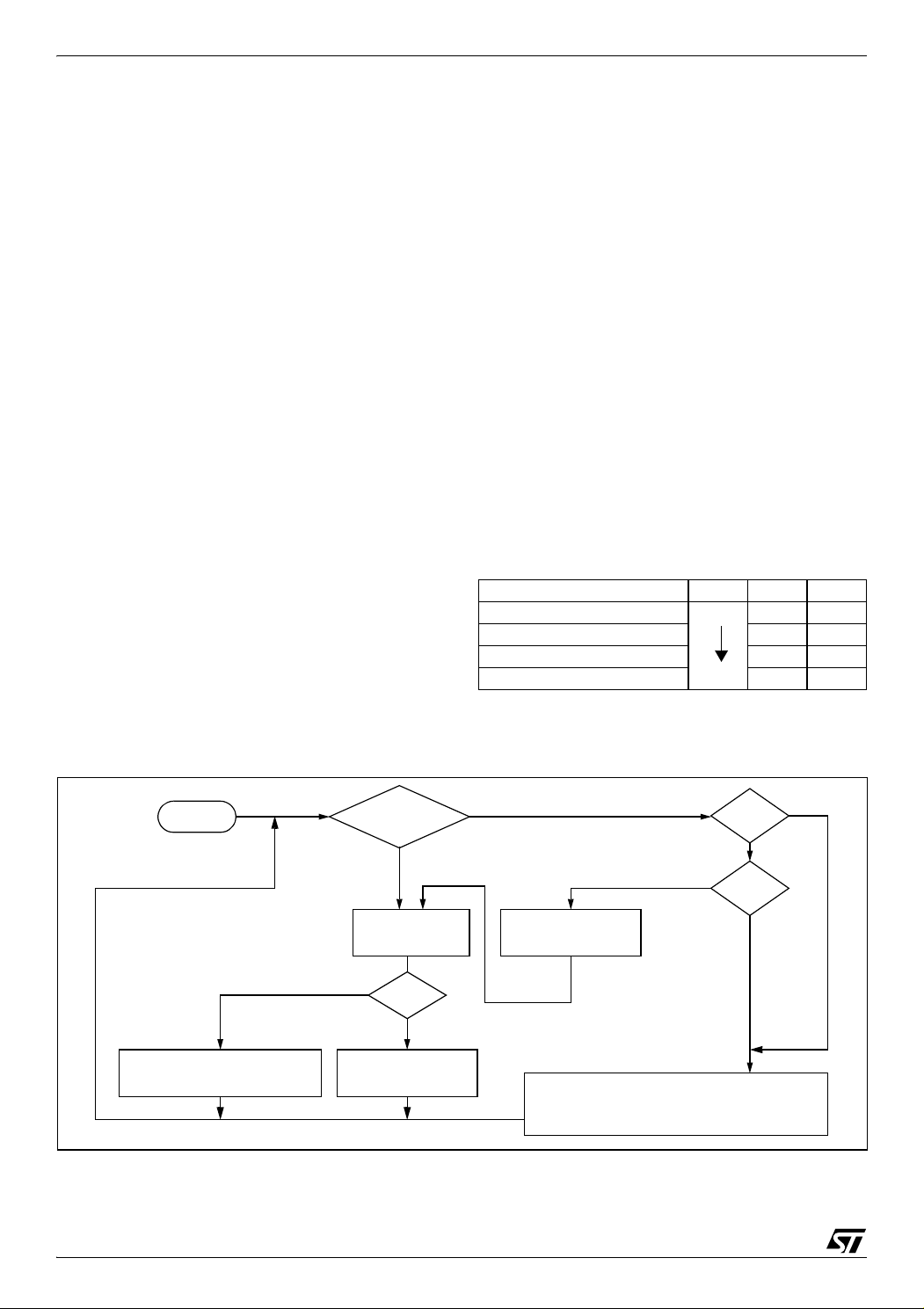
7 INTERRUPTS
7.1 INTRODUCTION
The CPU enhanced interrupt management provides the following features:
■ Hardware interrupts
■ Software interrupt (TRAP)
■ Nested or concurrent interrupt management
with flexible interrupt priority and level
management:
– Up to 4 software programmable nesting levels
– Up to 16 interrupt vectors fixed by hardware
– 3 non maskable events: RESET, TRAP, TLI
This interrupt management is based on:
– Bit 5 and bit 3 of the CPU CC register (I1:0),
– Interrupt software priority registers (ISPRx),
– Fixed interrupt vector addresses located at the
high addresses of the memory map (FFE0h to
FFFFh) sorted by hardware priority order.
This enhanced interrupt controller guarantees full
upward compatibility with the standard (not nested) CPU interrupt controller.
7.2 MASKING AND PROCESSING FLOW
The interrupt masking is managed by the I1 and I0
bits of the CC register and the ISPRx registers
which give the interrupt software priority level of
each interrupt vector (see Table 5). The processing flow is shown in Figure 20.
When an interrupt request has to be serviced:
– Normal processing is suspended at the end of
the current instruction execution.
– The PC, X, A and CC registers are saved onto
the stack.
– I1 and I0 bits of CC register are set according to
the corresponding values in the ISPRx registers
of the serviced interrupt vector.
– The PC is then loaded with the interrupt vector of
the interrupt to service and the first instruction of
the interrupt service routine is fetched (refer to
“Interrupt Mapping” table for vector addresses).
The interrupt service routine should end with the
IRET instruction which causes the contents of the
saved registers to be recovered from the stack.
Note: As a consequence of the IRET instruction,
the I1 and I0 bits will be restored from the stack
and the program in the previous level will resume.
Table 5. Interrupt Software Priority Levels
Interrupt software priority Level I1 I0
Level 0 (main)
Level 1 0 1
Level 2 0 0
Level 3 (= interrupt disable) 1 1
Low
High
10
Figure 20. Interrupt Processing Flowchart
24/139
Doc ID 6996 Rev 5

INTERRUPTS (Cont’d)
PENDING
SOFTWARE
Different
INTERRUPTS
Same
HIGHEST HARDWARE
PRIORITY SERVICED
PRIORITY
HIGHEST SOFTWARE
PRIORITY SERVICED
ST7262xxx
Servicing Pending Interrupts
As several interrupts can be pending at the same
time, the interrupt to be taken into account is determined by the following two-step process:
– the highest software priority interrupt is serviced,
– if several interrupts have the same software pri-
ority then the interrupt with the highest hardware
priority is serviced first.
Figure 21 describes this decision process.
Figure 21. Priority Decision Process
When an interrupt request is not serviced immediately, it is latched and then processed when its
software priority combined with the hardware priority becomes the highest one.
Note 1: The hardware priority is exclusive while
the software one is not. This allows the previous
process to succeed with only one interrupt.
Note 2: RESET, TRAP and TLI can be considered
as having the highest software priority in the decision process.
Different Interrupt Vector Sources
Two interrupt source types are managed by the
CPU interrupt controller: the non-maskable type
(RESET, TLI, TRAP) and the maskable type (external or from internal peripherals).
Non-Maskable Sources
These sources are processed regardless of the
state of the I1 and I0 bits of the CC register (see
Figure 20). After stacking the PC, X, A and CC
registers (except for RESET), the corresponding
vector is loaded in the PC register and the I1 and
I0 bits of the CC are set to disable interrupts (level
3). These sources allow the processor to exit
HALT mode.
■ TLI (Top Level Hardware Interrupt)
This hardware interrupt occurs when a specific
edge is detected on the dedicated TLI pin.
Caution: A TRAP instruction must not be used in a
TLI service routine.
■
TRAP (Non Maskable Software Interrupt)
This software interrupt is serviced when the TRAP
instruction is executed. It will be serviced according to the flowchart in Figure 20 as a TLI.
Caution: TRAP can be interrupted by a TLI.
■ RESET
The RESET source has the highest priority in the
CPU. This means that the first current routine has
the highest software priority (level 3) and the highest hardware priority.
See the RESET chapter for more details.
Maskable Sources
Maskable interrupt vector sources can be serviced
if the corresponding interrupt is enabled and if its
own interrupt software priority (in ISPRx registers)
is higher than the one currently being serviced (I1
and I0 in CC register). If any of these two conditions is false, the interrupt is latched and thus remains pending.
■ External Interrupts
External interrupts allow the processor to exit from
HALT low power mode.
External interrupt sensitivity is software selectable
through the ITRFRE2 register.
External interrupt triggered on edge will be latched
and the interrupt request automatically cleared
upon entering the interrupt service routine.
If several input pins of a group connected to the
same interrupt line are selected simultaneously,
these will be logically NANDed.
■ Peripheral Interrupts
Usually the peripheral interrupts cause the Device
to exit from HALT mode except those mentioned in
the “Interrupt Mapping” table.
A peripheral interrupt occurs when a specific flag
is set in the peripheral status registers and if the
corresponding enable bit is set in the peripheral
control register.
The general sequence for clearing an interrupt is
based on an access to the status register followed
by a read or write to an associated register.
Note: The clearing sequence resets the internal
latch. A pending interrupt (i.e. waiting for being
serviced) will therefore be lost if the clear sequence is executed.
Doc ID 6996 Rev 5
25/139

ST7262xxx
MAIN
IT4
IT2
IT1
TLI
IT1
MAIN
IT0
I1
HARDWARE PRIORITY
SOFTWARE
3
3
3
3
3
3/0
3
11
11
11
11
11
11 / 10
11
RIM
IT2
IT1
IT4
TLI
IT3
IT0
IT3
I0
10
PRIORITY
LEVEL
USED STACK = 10 BYTES
MAIN
IT2
TLI
MAIN
IT0
IT2
IT1
IT4
TLI
IT3
IT0
HARDWARE PRIORITY
3
2
1
3
3
3/0
3
11
00
01
11
11
11
RIM
IT1
IT4
IT4
IT1
IT2
IT3
I1 I0
11 / 10
10
SOFTWARE
PRIORITY
LEVEL
USED STACK = 20 BYTES
INTERRUPTS (Cont’d)
7.3 INTERRUPTS AND LOW POWER MODES
All interrupts allow the processor to exit the WAIT
low power mode. On the contrary, only external
and other specified interrupts allow the processor
to exit from the HALT modes (see column “Exit
from HALT” in “Interrupt Mapping” table). When
several pending interrupts are present while exiting HALT mode, the first one serviced can only be
an interrupt with exit from HALT mode capability
and it is selected through the same decision process shown in Figure 21.
Note: If an interrupt, that is not able to Exit from
HALT mode, is pending with the highest priority
when exiting HALT mode, this interrupt is serviced
after the first one serviced.
Figure 22. Concurrent Interrupt Management
7.4 CONCURRENT & NESTED MANAGEMENT
The following Figure 22 and Figure 23 show two
different interrupt management modes. The first is
called concurrent mode and does not allow an interrupt to be interrupted, unlike the nested mode in
Figure 23. The interrupt hardware priority is given
in this order from the lowest to the highest: MAIN,
IT4, IT3, IT2, IT1, IT0, TLI. The software priority is
given for each interrupt.
Warning: A stack overflow may occur without notifying the software of the failure.
Figure 23. Nested Interrupt Management
26/139
Doc ID 6996 Rev 5
INTERRUPTS (Cont’d)
ST7262xxx
7.5 INTERRUPT REGISTER DESCRIPTION
INTERRUPT SOFTWARE PRIORITY REGISTERS (ISPRX)
CPU CC REGISTER INTERRUPT BITS
Read/Write
Reset Value: 111x 1010 (xAh)
70
11I1 H I0 NZC
Bit 5, 3 = I1, I0 Software Interrupt Priority
These two bits indicate the current interrupt soft-
ware priority.
Interrupt Software Priority Level I1 I0
Level 0 (main)
Level 1 0 1
Level 2 0 0
Level 3 (= interrupt disable*) 1 1
Low
High
10
These two bits are set/cleared by hardware when
entering in interrupt. The loaded value is given by
the corresponding bits in the interrupt software priority registers (ISPRx).
They can be also set/cleared by software with the
RIM, SIM, HALT, WFI, IRET and PUSH/POP instructions (see “Interrupt Dedicated Instruction
Set” table).
*Note: TLI, TRAP and RESET events can interrupt
a level 3 program.
Read/Write (bit 7:4 of ISPR3 are read only)
Reset Value: 1111 1111 (FFh)
70
ISPR0 I1_3 I0_3 I1_2 I0_2 I1_1 I0_1 I1_0 I0_0
ISPR1 I1_7 I0_7 I1_6 I0_6 I1_5 I0_5 I1_4 I0_4
ISPR2 I1_11 I0_11 I1_10 I0_10 I1_9 I0_9 I1_8 I0_8
ISPR3 1 1 1 1 I1_13 I0_13 I1_12 I0_12
These four registers contain the interrupt software
priority of each interrupt vector.
– Each interrupt vector (except RESET and TRAP)
has corresponding bits in these registers where
its own software priority is stored. This correspondence is shown in the following table.
Vector address ISPRx bits
FFFBh-FFFAh I1_0 and I0_0 bits*
FFF9h-FFF8h I1_1 and I0_1 bits
... ...
FFE1h-FFE0h I1_13 and I0_13 bits
– Each I1_x and I0_x bit value in the ISPRx regis-
ters has the same meaning as the I1 and I0 bits
in the CC register.
– Level 0 can not be written (I1_x=1, I0_x=0). In
this case, the previously stored value is kept. (example: previous=CFh, write=64h, result=44h)
The RESET, TRAP and TLI vectors have no software priorities. When one is serviced, the I1 and I0
bits of the CC register are both set.
*Note: Bits in the ISPRx registers which correspond to the TLI can be read and written but they
are not significant in the interrupt process management.
Caution: If the I1_x and I0_x bits are modified
while the interrupt x is executed the following behaviour has to be considered: If the interrupt x is
still pending (new interrupt or flag not cleared) and
the new software priority is higher than the previous one, the interrupt x is re-entered. Otherwise,
the software priority stays unchanged up to the
next interrupt request (after the IRET of the interrupt x).
Doc ID 6996 Rev 5
27/139

ST7262xxx
INTERRUPTS (Cont’d)
INTERRUPT REGISTER 1 (ITRFRE1)
Address: 0008h - Read/Write
Reset Value: 0000 0000 (00h)
70
IT8E IT7E IT6E IT5E IT4E IT3E IT2E IT1E
Bit 7:0 = ITiE Interrupt Enable
0: I/O pin free for general purpose I/O
1: ITi external interrupt enabled.
Note: The corresponding interrupt is generated
when:
– a rising edge occurs on the IT5/IT6 pins
– a falling edge occurs on the IT1, 2, 3, 4, 7 and 8
pins
INTERRUPT REGISTER 2 (ITRFRE2)
Address: 0039h - Read/Write
Reset Value: 0000 0000 (00h)
Bit 5:4 = CTL[1:0] IT[10:9]1nterrupt Sensitivity
These bits are set and cleared by software. They
are used to configure the edge and level sensitivity
of the IT10 and IT9 external interrupt pins (this
means that both must have the same sensitivity).
CTL1 CTL0 IT[10:9] Sensitivity
0 0 Falling edge and low level
0 1 Rising edge only
1 0 Falling edge only
1 1 Rising and falling edge
Bit 3:0 = ITiE Interrupt Enable
0: I/O pin free for general purpose I/O
1: ITi external interrupt enabled.
70
CTL3 CTL2 CTL1 CTL0 IT12E IT11E IT10E IT9E
Bit 7:6 = CTL[3:2] IT[12:11] Interrupt Sensitivity
These bits are set and cleared by software. They
are used to configure the edge and level sensitivity
of the IT12 and IT11 external interrupt pins (this
means that both must have the same sensitivity).
CTL3 CTL2 IT[12:11] Sensitivity
0 0 Falling edge and low level
0 1 Rising edge only
1 0 Falling edge only
1 1 Rising and falling edge
28/139
Doc ID 6996 Rev 5

INTERRUPTS (Cont’d)
Table 6. Interrupt Mapping
ST7262xxx
N°
0 ICP FLASH Start programming NMI interrupt Yes FFFAh-FFFBh
1 USB USB End Suspend interrupt USBISTR Yes FFF8h-FFF9h
2
3 Port B external interrupts IT[8:5] ITRFRE1 Yes FFF4h-FFF5h
4 Port C external interrupts IT[12:9] ITRFRE2 Yes FFF2h-FFF3h
5 TBU Timebase Unit interrupt TBUCSR No FFF0h-FFF1h
6 ART ART/PWM Timer interrupt ICCSR Yes FFEEh-FFEFh
7 SPI SPI interrupt vector SPISR Yes FFECh-FFEDh
8 SCI SCI interrupt vector SCISR No FFEAh-FFEBh
9 USB USB interrupt vector USBISTR No FFE8h-FFE9h
10 ADC A/D End of conversion interrupt ADCCSR No FFE6h-FFE7h
Source
Block
I/O Ports
Description
Reset
TRAP software interrupt No FFFCh-FFFDh
Port A external interrupts IT[4:1] ITRFRE1 Yes FFF6h-FFF7h
Reserved area FFE0h-FFE5h
Register
Label
Priority
Order
Highest
Priority
Lowest
Priority
Exit
from
HALT
Yes FFFEh-FFFFh
Address
Vector
Table 7. Nested Interrupts Register Map and Reset Values
Address
(Hex.)
Register
Label
76543210
0032h
0033h
0034h
0035h
Ext. Interrupt Port B Ext. Interrupt Port A USB END SUSP Not Used
ISPR0
Reset Value
ISPR1
Reset Value
ISPR2
Reset Value
ISPR3
Reset Value1111
I1_3
1
I1_7
1
Not Used ADC USB SCI
I1_11
1
I0_3
1
SPI ART TBU Ext. Interrupt Port C
I0_7
1
I0_11
1
I1_2
1
I1_6
1
I1_10
1
I0_2
1
I0_6
1
I0_10
1
I1_13
I1_1
1
I1_5
1
I1_9
1
Not Used Not Used
1
I0_1
111
I0_5
1
I0_9
1
I0_13
1
I1_4
1
I1_8
1
I1_12
1
I0_4
1
I0_8
1
I0_12
1
Doc ID 6996 Rev 5
29/139

ST7262xxx
WFI INSTRUCTION
RESET
INTERRUPT
Y
N
N
Y
CPU CLOCK
OSCILLATOR
PERIPH. CLOCK
I-BIT
ON
ON
CLEARED
OFF
CPU CLOCK
OSCILLATOR
PERIPH. CLOCK
I-BIT
ON
ON
SET
ON
FETCH RESET VECTOR
OR SERVICE INTERRUPT
514 CPU CLOCK
CYCLES DELAY
IF RESET
Note: Before servicing an interrupt, the CC register is
pushed on the stack. The I-Bit is set during the interrupt routine and cleared when the CC register is
popped.
8 POWER SAVING MODES
8.1 INTRODUCTION
There are three Power Saving modes. Slow Mode
is selected by setting the SMS bits in the Miscellaneous register. Wait and Halt modes may be entered using the WFI and HALT instructions.
After a RESET the normal operating mode is selected by default (RUN mode). This mode drives
the device (CPU and embedded peripherals) by
means of a master clock which is based on the
main oscillator frequency divided by 3 and multiplied by 2 (f
CPU
).
From Run mode, the different power saving
modes may be selected by setting the relevant
register bits or by calling the specific ST7 software
instruction whose action depends on the oscillator
status.
8.1.1 Slow Mode
In Slow mode, the oscillator frequency can be divided by a value defined in the Miscellaneous
Register. The CPU and peripherals are clocked at
this lower frequency. Slow mode is used to reduce
power consumption, and enables the user to adapt
clock frequency to available supply voltage.
Figure 24. WAIT Mode Flow Chart
8.2 WAIT MODE
WAIT mode places the MCU in a low power consumption mode by stopping the CPU.
This power saving mode is selected by calling the
“WFI” ST7 software instruction.
All peripherals remain active. During WAIT mode,
the I bit of the CC register is forced to 0, to enable
all interrupts. All other registers and memory remain unchanged. The MCU remains in WAIT
mode until an interrupt or Reset occurs, whereupon the Program Counter branches to the starting
address of the interrupt or Reset service routine.
The MCU will remain in WAIT mode until a Reset
or an Interrupt occurs, causing it to wake up.
Refer to Figure 24.
30/139
Doc ID 6996 Rev 5

ST7262xxx
N
N
EXTERNAL
INTERRUPT*
RESET
HALT INSTRUCTION
514 CPU CLOCK
FETCH RESET VECTOR
OR SERVICE INTERRUPT
CYCLES DELAY
CPU CLOCK
OSCILLATOR
PERIPH. CLOCK
I-BIT
ON
ON
SET
ON
CPU CLOCK
OSCILLATOR
PERIPH. CLOCK
I-BIT
OFF
OFF
CLEARED
OFF
Y
Y
Note: Before servicing an interrupt, the CC register is
pushed on the stack. The I-Bit is set during the interrupt routine and cleared when the CC register is
popped.
POWER SAVING MODES (Cont’d)
8.3 HALT MODE
The HALT mode is the MCU lowest power consumption mode. The HALT mode is entered by executing the HALT instruction. The internal oscillator is then turned off, causing all internal processing to be stopped, including the operation of the
on-chip peripherals.
When entering HALT mode, the I bit in the Condition Code Register is cleared. Thus, any of the external interrupts (ITi or USB end suspend mode),
are allowed and if an interrupt occurs, the CPU
clock becomes active.
The MCU can exit HALT mode on reception of either an external interrupt on ITi, an end suspend
mode interrupt coming from USB peripheral, or a
reset. The oscillator is then turned on and a stabilization time is provided before releasing CPU operation. The stabilization time is 514 CPU clock cycles.
After the start up delay, the CPU continues operation by servicing the interrupt which wakes it up or
by fetching the reset vector if a reset wakes it up.
Figure 25. HALT Mode Flow Chart
Doc ID 6996 Rev 5
31/139

ST7262xxx
9 I/O PORTS
9.1 INTRODUCTION
The I/O ports offer different functional modes:
transfer of data through digital inputs and outputs
and for specific pins:
– Analog signal input (ADC)
– Alternate signal input/output for the on-chip pe-
ripherals.
– External interrupt generation
An I/O port is composed of up to 8 pins. Each pin
can be programmed independently as digital input
or digital output.
9.2 FUNCTIONAL DESCRIPTION
Each port is associated with 2 main registers:
– Data Register (DR)
– Data Direction Register (DDR)
Each I/O pin may be programmed using the corre-
sponding register bits in DDR register: bit x corresponding to pin x of the port. The same correspondence is used for the DR register.
Table 8. I/O Pin Functions
DDR MODE
0 Input
1 Output
9.2.1 Input Modes
The input configuration is selected by clearing the
corresponding DDR register bit.
In this case, reading the DR register returns the
digital value applied to the external I/O pin.
Notes:
1. All the inputs are triggered by a Schmitt trigger.
2. When switching from input mode to output
mode, the DR register should be written first to
output the correct value as soon as the port is
configured as an output.
Interrupt function
When an external interrupt function of an I/O pin, is
enabled using the ITFRE registers, an event on
this I/O can generate an external Interrupt request
to the CPU. The interrupt sensitivity is programma-
ble, the options are given in the description of the
ITRFRE interrupt registers.
Each pin can independently generate an Interrupt
request.
Each external interrupt vector is linked to a dedicated group of I/O port pins (see Interrupts section). If more than one input pin is selected simultaneously as interrupt source, this is logically ANDed and inverted. For this reason, if an event occurs on one of the interrupt pins, it masks the other
ones.
9.2.2 Output Mode
The pin is configured in output mode by setting the
corresponding DDR register bit (see Table 7).
In this mode, writing “0” or “1” to the DR register
applies this digital value to the I/O pin through the
latch. Then reading the DR register returns the
previously stored value.
Note: In this mode, the interrupt function is disabled.
9.2.3 Alternate Functions
Digital Alternate Functions
When an on-chip peripheral is configured to use a
pin, the alternate function is automatically selected. This alternate function takes priority over
standard I/O programming. When the signal is
coming from an on-chip peripheral, the I/O pin is
automatically configured in output mode (push-pull
or open drain according to the peripheral).
When the signal is going to an on-chip peripheral,
the I/O pin has to be configured in input mode. In
this case, the pin state is also digitally readable by
addressing the DR register.
Notes:
1. Input pull-up configuration can cause an unexpected value at the alternate peripheral input.
2. When the on-chip peripheral uses a pin as input
and output, this pin must be configured as an
input (DDR = 0).
Warning: Alternate functions of peripherals must
must not be activated when the external interrupts
are enabled on the same pin, in order to avoid
generating spurious interrupts.
32/139
Doc ID 6996 Rev 5

I/O PORTS (Cont’d)
Analog Alternate Functions
When the pin is used as an ADC input, the I/O
must be configured as input. The analog multiplexer (controlled by the ADC registers) switches the
analog voltage present on the selected pin to the
common analog rail which is connected to the
ADC input.
It is recommended not to change the voltage level
or loading on any port pin while conversion is in
progress. Furthermore it is recommended not to
ST7262xxx
have clocking pins located close to a selected analog pin.
Warning: The analog input voltage level must be
within the limits stated in the Absolute Maximum
Ratings.
9.2.4 I/O Port Implementation
The hardware implementation on each I/O port depends on the settings in the DDR register and specific features of the I/O port such as ADC Input or
true open drain.
Doc ID 6996 Rev 5
33/139

ST7262xxx
DR
DDR
LATCH
LATCH
DR SEL
DDR SEL
V
DD
PA D
ANALOG
SWITCH
ANALOG ENABLE
(ADC)
ALTERNATE ENABLE
ALTERNATE ENABLE
DIGITAL ENABLE
ALTERNATE ENABLE
ALTERNATE
ALTERNATE INPUT
OUTPUT
P-BUFFER
N-BUFFER
1
0
1
0
V
SS
DATA BUS
COMMON ANALOG RAIL
V
DD
DIODES
I/O PORTS (Cont’d)
9.2.5 Port A
Table 9. Port A Description
PORT A
Input* Output Signal Condition
I/O Alternate Function
USBOE USBOE = 1 (MISC)
PA0 floating push-pull
IT1 Schmitt triggered input IT1E = 1 (ITRFRE1)
AIN0 (ADC) CS[2:0] = 000 (ADCCSR)
PA1 floating push-pull
PA2 floating push-pull
PA3 floating push-pull
IT2 Schmitt triggered input IT2E = 1 (ITRFRE1)
AIN1 (ADC) CS[2:0] = 001 (ADCCSR)
IT3 Schmitt triggered input IT3E = 1 (ITRFRE1)
AIN2 (ADC) CS[2:0] = 010 (ADCCSR)
IT4 Schmitt triggered input IT4E = 1 (ITRFRE1)
AIN3 (ADC) CS[2:0] = 011 (ADCCSR)
PA4 floating push-pull AIN4 (ADC) CS[2:0] = 100 (ADCCSR)
PA5 floating push-pull AIN5 (ADC) CS[2:0] = 101 (ADCCSR)
PA6 floating push-pull AIN6 (ADC) CS[2:0] = 110 (ADCCSR)
PA7 floating push-pull AIN7 (ADC) CS[2:0] = 111 (ADCCSR)
*Reset State
Figure 26. PA[7:0] Configuration
34/139
Doc ID 6996 Rev 5

I/O PORTS (Cont’d)
DR
DDR
LATCH
LATCH
DR SEL
DDR SEL
V
DD
PA D
ALTERNATE ENABLE
ALTERNATE ENABLE
ALTERNATE ENABLE
ALTERNATE
ALTERNATE INPUT
OUTPUT
P-BUFFER
N-BUFFER
1
0
1
0
CMOS SCHMITT TRIGGER
V
SS
V
DD
DIODES
DATA BUS
PULL-UP*
* PULL-UP ON PORT C [7:2] ONLY
9.2.6 Port B
Table 10. Port B Description
ST7262xxx
PORT B
I/O Alternate Function
Input* Output Signal Condition
PB0 floating push-pull (high sink) MCO (Main Clock Output) MCO = 1 (MISCR)
PB1 floating push-pull (high sink) RDI SCI enabled
PB2 floating push-pull (high sink) TDO TE = 1 (SCICR2)
PB3 floating push-pull (high sink) ARTCLK EXCL = 1 (ARTCSR)
ARTIC1 ART Timer enabled
PB4 floating push-pull (high sink)
IT5 Schmitt triggered input IT5E = 1 (ITRFRE1)
ARTIC2 ART Timer enabled
PB5 floating push-pull (high sink)
IT6 Schmitt triggered input IT6E = 1 (ITRFRE1)
PWM1 OE0 = 1 (PWMCR)
PB6 floating push-pull (high sink)
IT7 Schmitt triggered input IT7E = 1 (ITRFRE1)
PWM2 OE1 = 1 (PWMCR)
PB7 floating push-pull (high sink)
IT8 Schmitt triggered input IT8E = 1 (ITRFRE1)
*Reset State
Figure 27. Port B and Port C [7:2] Configuration
Doc ID 6996 Rev 5
35/139

ST7262xxx
DR
DDR
LATCH
LATCH
DR SEL
DDR SEL
PA D
ALTERNATE ENABLE
ALTERNATE ENABLE
ALTERNATE
OUTPUT
N-BUFFER
1
0
1
0
CMOS SCHMITT TRIGGER
V
SS
DIODES
DATA BUS
I/O PORTS (Cont’d)
9.2.7 Port C
Table 11. Port C Description
PORT C
I/O Alternate Function
Input* Output Signal Condition
PC0 floating true open drain
PC1 floating true open drain
PC2 with pull-up push-pull IT9 Schmitt triggered input IT9E = 1 (ITRFRE2)
SCK SPI enabled
PC3 with pull-up push-pull
IT10 Schmitt triggered input IT10E = 1 (ITRFRE2)
SPI enabled
SS
PC4 with pull-up push-pull
IT11 Schmitt triggered input IT11E = 1 (ITRFRE2)
MISO SPI enabled
PC5 with pull-up push-pull
IT12 Schmitt triggered input IT12E = 1 (ITRFRE2)
PC6 with pull-up push-pull MOSI SPI enabled
PC7 with pull-up push-pull
*Reset State
Figure 28. Port C[1:0] Configuration
36/139
Doc ID 6996 Rev 5

I/O PORTS (Cont’d)
DR
DDR
LATCH
LATCH
DR SEL
DDR SEL
V
DD
PA D
ALTERNATE ENABLE
ALTERNATE ENABLE
ALTERNATE ENABLE
ALTERNATE
ALTERNATE INPUT
PULL-UP
OUTPUT
P-BUFFER
N-BUFFER
1
0
1
0
CMOS SCHMITT TRIGGER
V
SS
V
DD
DATA BUS
DIODES
9.2.8 Port D
Table 12. Port D Description
ST7262xxx
PORT D
I/O Alternate Function
Input* Output Signal Condition
PD0 with pull-up push-pull
PD1 with pull-up push-pull
PD2 with pull-up push-pull
PD3 with pull-up push-pull
PD4 with pull-up push-pull
PD5 with pull-up push-pull
PD6 with pull-up push-pull
*Reset State
Figure 29. Port D Configuration
Doc ID 6996 Rev 5
37/139

ST7262xxx
I/O PORTS (Cont’d)
9.2.9 Register Description
DATA REGISTER (DR)
Port x Data Register
PxDR with x = A, B, C or D.
Read/Write
Reset Value: 0000 0000 (00h)
70
D7 D6 D5 D4 D3 D2 D1 D0
DATA DIRECTION REGISTER (DDR)
Port x Data Direction Register
PxDDR with x = A, B, C or D.
Read/Write
Reset Value: 0000 0000 (00h)
70
DD7 DD6 DD5 DD4 DD3 DD2 DD1 DD0
Bits 7:0 = DD[7:0] Data direction register 8 bits.
Bits 7:0 = D[7:0] Data register 8 bits.
The DR register has a specific behaviour accord-
ing to the selected input/output configuration. Writing the DR register is always taken into account
even if the pin is configured as an input; this allows
The DDR register gives the input/output direction
configuration of the pins. Each bit is set and
cleared by software.
0: Input mode
1: Output mode
to always have the expected level on the pin when
toggling to output mode. Reading the DR register
returns either the DR register latch content (pin
configured as output) or the digital value applied to
the I/O pin (pin configured as input).
38/139
Doc ID 6996 Rev 5

I/O PORTS (Cont’d)
Table 13. I/O Port Register Map and Reset Values
ST7262xxx
Address
(Hex.)
Reset Value
of all I/O port registers
0000h PADR
0001h PADDR
0002h PBDR
0003h PBDDR
0004h PCDR
0005h PCDDR
0006h PDDR
0007h PDDDR
Register
Label
76543210
00000000
MSB LSB
MSB LSB
MSB LSB
MSB LSB
Doc ID 6996 Rev 5
39/139

ST7262xxx
9.3 MISCELLANEOUS REGISTER
MISCELLANEOUS REGISTER
Read Write
Reset Value - 0000 0000 (00h)
Bit 1 = USBOE USB Output Enable
0: PA0 port free for general purpose I/O
1: USBOE alternate function enabled. The USB
output enable signal is output on the PA0 port
70
----SMS1SMS0
US-
BOE
MCO
(at “1” when the ST7 USB is transmitting data).
Bit 0 = MCO Main Clock Out
0: PB0 port free for general purpose I/O
Bits 7:4 = Reserved
1: MCO alternate function enabled (f
PB0 I/O port)
Bits 3:2 = SMS[1:0] Slow Mode Selection
These bits select the Slow Mode frequency (depending on the oscillator frequency configured by
option byte).
OSC12/6 SMS1 SMS0
00 4
f
OSC
f
OSC
= 6 MHz.
= 12 MHz.
01 2
10 1
11 0.5
00 8
01 4
10 2
11 1
Slow Mode Frequency
(MHz.)
output on
CPU
40/139
Doc ID 6996 Rev 5

10 ON-CHIP PERIPHERALS
RESET
WDGA
7-BIT DOWNCOUNTER
f
CPU
T6
T0
CLOCK DIVIDER
WATCHDOG CONTROL REGISTER (CR)
÷65536
T1
T2
T3
T4
T5
10.1 WATCHDOG TIMER (WDG)
ST7262xxx
10.1.1 Introduction
The Watchdog timer is used to detect the occurrence of a software fault, usually generated by external interference or by unforeseen logical conditions, which causes the application program to
abandon its normal sequence. The Watchdog circuit generates an MCU reset on expiry of a programmed time period, unless the program refreshes the counter’s contents before the T6 bit becomes cleared.
10.1.2 Main Features
■ Programmable free-running downcounter (64
increments of 65536 CPU cycles)
■ Programmable reset
■ Reset (if watchdog activated) when the T6 bit
reaches zero
■ Hardware Watchdog selectable by option byte
10.1.3 Functional Description
The counter value stored in the CR register (bits
T[6:0]), is decremented every 65,536 machine cycles, and the length of the timeout period can be
programmed by the user in 64 increments.
Figure 30. Watchdog Block Diagram
If the watchdog is activated (the WDGA bit is set)
and when the 7-bit timer (bits T[6:0]) rolls over
from 40h to 3Fh (T6 becomes cleared), it initiates
a reset cycle by driving low the reset pin for 30µs.
The application program must write in the CR register at regular intervals during normal operation to
prevent an MCU reset. This downcounter is freerunning: it counts down even if the watchdog is diabled The value to be stored in the CR register
must be between FFh and C0h (see Table 14):
– The WDGA bit is set (watchdog enabled)
– The T6 bit is set to prevent generating an imme-
diate reset
– The T[5:0] bits contain the number of increments
which represents the time delay before the
watchdog produces a reset.
Table 14.Watchdog Timing (f
CR Register
initial value
Max FFh 524.288
Min C0h 8.192
= 8 MHz)
CPU
WDG timeout period
(ms)
Doc ID 6996 Rev 5
41/139

ST7262xxx
WATCHDOG TIMER (Cont’d)
10.1.4 Software Watchdog Option
If Software Watchdog is selected by option byte,
the watchdog is disabled following a reset. Once
activated it cannot be disabled, except by a reset.
The T6 bit can be used to generate a software reset (the WDGA bit is set and the T6 bit is cleared).
10.1.5 Hardware Watchdog Option
If Hardware Watchdog is selected by option byte,
the watchdog is always active and the WDGA bit in
the CR is not used.
– The opcode for the HALT instruction is 0x8E. To
avoid an unexpected HALT instruction due to a
program counter failure, it is advised to clear all
occurrences of the data value 0x8E from memory. For example, avoid defining a constant in
ROM with the value 0x8E.
– As the HALT instruction clears the I bit in the CC
register to allow interrupts, the user may choose
to clear all pending interrupt bits before executing the HALT instruction. This avoids entering
other peripheral interrupt routines after executing
the external interrupt routine corresponding to
the wake-up event (reset or external interrupt).
10.1.6 Low Power Modes
WAIT Instruction
No effect on Watchdog.
HALT Instruction
Halt mode can be used when the watchdog is enabled. When the oscillator is stopped, the WDG
stops counting and is no longer able to generate a
reset until the microcontroller receives an external
interrupt or a reset.
If an external interrupt is received, the WDG restarts counting after 514 CPU clocks. In the case
of the Software Watchdog option, if a reset is generated, the WDG is disabled (reset state).
Recommendations
– Make sure that an external event is available to
wake up the microcontroller from Halt mode.
– Before executing the HALT instruction, refresh
the WDG counter, to avoid an unexpected WDG
reset immediately after waking up the microcontroller.
– When using an external interrupt to wake up the
microcontroller, reinitialize the corresponding I/O
as Input before executing the HALT instruction.
The main reason for this is that the I/O may be
wrongly configured due to external interference
or by an unforeseen logical condition.
10.1.7 Interrupts
None.
10.1.8 Register Desc4ription
CONTROL REGISTER (CR)
Read/Write
Reset Value: 0111 1111 (7Fh)
70
WDGA T6 T5 T4 T3 T2 T1 T0
Bit 7 = WDGA Activation bit.
This bit is set by software and only cleared by
hardware after a reset. When WDGA = 1, the
watchdog can generate a reset.
0: Watchdog disabled
1: Watchdog enabled
Note: This bit is not used if the hardware watchdog option is enabled by option byte.
Bits 6:0 = T[6:0] 7-bit timer (MSB to LSB).
These bits contain the decremented value. A reset
is produced when it rolls over from 40h to 3Fh (T6
becomes cleared).
Table 15. Watchdog Timer Register Map and Reset Values
Address
(Hex.)
0Dh
42/139
Register
Label
WDGCR
Reset Value
76543210
WDGA
0
T6
T5
1
1
Doc ID 6996 Rev 5
T4
1
T3
T2
1
1
T1
T0
1
1

10.2 PWM AUTO-RELOAD TIMER (ART)
OVF INTERRUPT
EXCL CC2 CC1 CC0 TCE FCRL OIE OVF
ARTCSR
f
INPUT
PWMx
PORT
FUNCTION
ALTERNATE
OCRx
COMPARE
REGISTER
PROGRAMMABLE
PRESCALER
8-BIT COUNTER
(ARTCAR REGISTER)
ARTARR
REGISTER
ARTICRx
REGISTER
LOAD
OPx
POLARITY
CONTROL
OEx
PWMCR
MUX
f
CPU
PWMDCRx
REGISTER
LOAD
f
COUNTER
ARTCLK
f
EXT
ARTICx
ICFxICSx
ARTICCSR
LOAD
ICx INTERRUPT
ICIEx
INPUT CAPTURE
CONTROL
10.2.1 Introduction
The Pulse Width Modulated Auto-Reload Timer
on-chip peripheral consists of an 8-bit auto reload
counter with compare/capture capabilities and of a
7-bit prescaler clock source.
These resources allow five possible operating
modes:
– Generation of up to 2 independent PWM signals
– Output compare and Time base interrupt
Figure 31. PWM Auto-Reload Timer Block Diagram
ST7262xxx
– Up to two input capture functions
– External event detector
– Up to two external interrupt sources
The three first modes can be used together with a
single counter frequency.
The timer can be used to wake up the MCU from
WAIT and HALT modes.
Doc ID 6996 Rev 5
43/139

ST7262xxx
COUNTER
FDh FEh FFh FDh FEh FFh FDh FEh
ARTARR=FDh
f
COUNTER
OCRx
PWMDCRx
FDh
FEh
FDh
FEh
FFh
PWMx
PWM AUTO-RELOAD TIMER (Cont’d)
10.2.2 Functional Description
Counter
The free running 8-bit counter is fed by the output
of the prescaler, and is incremented on every rising edge of the clock signal.
It is possible to read or write the contents of the
counter on the fly by reading or writing the Counter
Access register (ARTCAR).
When a counter overflow occurs, the counter is
automatically reloaded with the contents of the
ARTARR register (the prescaler is not affected).
Counter clock and prescaler
The counter clock frequency is given by:
f
COUNTER
= f
INPUT
The timer counter’s input clock (f
/ 2
CC[2:0]
INPUT
) feeds the
7-bit programmable prescaler, which selects one
of the 8 available taps of the prescaler, as defined
by CC[2:0] bits in the Control/Status Register
(ARTCSR). Thus the division factor of the prescaler can be set to 2
This f
INPUT
n
(where n = 0, 1,..7).
frequency source is selected through
the EXCL bit of the ARTCSR register and can be
either the f
or an external input frequency f
CPU
EXT
The clock input to the counter is enabled by the
TCE (Timer Counter Enable) bit in the ARTCSR
register. When TCE is reset, the counter is
stopped and the prescaler and counter contents
are frozen. When TCE is set, the counter runs at
the rate of the selected clock source.
Counter and Prescaler Initialization
After RESET, the counter and the prescaler are
cleared and f
INPUT
= f
CPU
.
The counter can be initialized by:
– Writing to the ARTARR register and then setting
the FCRL (Force Counter Re-Load) and the TCE
(Timer Counter Enable) bits in the ARTCSR reg-
ister.
– Writing to the ARTCAR counter access register,
In both cases the 7-bit prescaler is also cleared,
whereupon counting will start from a known value.
Direct access to the prescaler is not possible.
Output compare control
The timer compare function is based on four different comparisons with the counter (one for each
PWMx output). Each comparison is made between the counter value and an output compare
register (OCRx) value. This OCRx register can not
be accessed directly, it is loaded from the duty cycle register (PWMDCRx) at each overflow of the
counter.
.
This double buffering method avoids glitch generation when changing the duty cycle on the fly.
Figure 32. Output compare control
44/139
Doc ID 6996 Rev 5

PWM AUTO-RELOAD TIMER (Cont’d)
DUTY CYCLE
REGISTER
AUTO-RELOAD
REGISTER
PWMx OUTPUT
t
255
000
WITH OEx=1
AND OPx=0
(ARTARR)
(PWMDCRx)
WITH OEx=1
AND OPx=1
COUNTER
ST7262xxx
Independent PWM signal generation
This mode allows up to two Pulse Width Modulated signals to be generated on the PWMx output
pins with minimum core processing overhead.
This function is stopped during HALT mode.
Each PWMx output signal can be selected independently using the corresponding OEx bit in the
PWM Control register (PWMCR). When this bit is
set, the corresponding I/O pin is configured as output push-pull alternate function.
The PWM signals all have the same frequency
which is controlled by the counter period and the
ARTARR register value.
f
PWM
= f
COUNTER
/ (256 - ARTARR)
When a counter overflow occurs, the PWMx pin
level is changed depending on the corresponding
OPx (output polarity) bit in the PWMCR register.
Figure 33. PWM Auto-reload Timer Function
When the counter reaches the value contained in
one of the output compare register (OCRx) the
corresponding PWMx pin level is restored.
It should be noted that the reload values will also
affect the value and the resolution of the duty cycle
of the PWM output signal. To obtain a signal on a
PWMx pin, the contents of the OCRx register must
be greater than the contents of the ARTARR register.
The maximum available resolution for the PWMx
duty cycle is:
Resolution = 1 / (256 - ARTARR)
Note: To get the maximum resolution (1/256), the
ARTARR register must be 0. With this maximum
resolution, 0% and 100% can be obtained by
changing the polarity.
Doc ID 6996 Rev 5
45/139

ST7262xxx
COUNTER
PWMx OUTPUT
t
WITH OEx=1
AND OPx=0
FDh FEh FFh FDh FEh FFh FDh FEh
OCRx=FCh
OCRx=FDh
OCRx=FEh
OCRx=FFh
ARTARR=FDh
f
COUNTER
Figure 34. PWM Signal from 0% to 100% Duty Cycle
46/139
Doc ID 6996 Rev 5

PWM AUTO-RELOAD TIMER (Cont’d)
COUNTER
t
FDh FEh FFh FDh
OVF
ARTCSR READ
INTERRUPT
ARTARR=FDh
f
EXT=fCOUNTER
FEh FFh FDh
IF OIE=1
INTERRUPT
IF OIE=1
ARTCSR READ
ST7262xxx
Output compare and Time base interrupt
On overflow, the OVF flag of the ARTCSR register
is set and an overflow interrupt request is generated if the overflow interrupt enable bit, OIE, in the
ARTCSR register, is set. The OVF flag must be reset by the user software. This interrupt can be
External clock and event detector mode
Using the f
auto-reload timer can be used as an external clock
event detector. In this mode, the ARTARR register
is used to select the n
be counted before setting the OVF flag.
used as a time base in the application.
When entering HALT mode while f
all the timer control registers are frozen but the
counter continues to increment. If the OIE bit is
set, the next overflow of the counter will generate
an interrupt which wakes up the MCU.
Caution: If HALT mode is used in the application,
prior to executing the HALT instruction, the counter must be disabled by clearing the TCE bit in the
ARTCSR register to avoid spurious counter increments.
Figure 35. External Event Detector Example (3 counts)
external prescaler input clock, the
EXT
number of events to
EVENT
n
= 256 - ARTARR
EVENT
is selected,
EXT
Doc ID 6996 Rev 5
47/139

ST7262xxx
ARTICx PIN
CFx FLAG
t
f
COUNTER
INTERRUPT
COUNTER
t
01h
f
COUNTER
xxh
02h
03h 04h 05h 06h 07h
04h
ARTICx PIN
CFx FLAG
ICRx REGISTER
INTERRUPT
PWM AUTO-RELOAD TIMER (Cont’d)
Input capture function
This mode allows the measurement of external
signal pulse widths through ICRx registers.
Each input capture can generate an interrupt independently on a selected input signal transition.
This event is flagged by a set of the corresponding
CFx bits of the Input Capture Control/Status register (ICCSR).
These input capture interrupts are enabled
through the CIEx bits of the ICCSR register.
The active transition (falling or rising edge) is software programmable through the CSx bits of the
ICCSR register.
The read only input capture registers (ICRx) are
used to latch the auto-reload counter value when a
transition is detected on the ARTICx pin (CFx bit
set in ICCSR register). After fetching the interrupt
vector, the CFx flags can be read to identify the interrupt source.
Note: After a capture detection, data transfer in
the ICRx register is inhibited until the ARTICCSR
register is read (clearing the CFx bit).
The timer interrupt remains pending while the CFx
flag is set when the interrupt is enabled (CIEx bit
set). This means, the ARTICCSR register has to
be read at each capture event to clear the CFx
flag.
During HALT mode, input capture is inhibited (the
ICRx is never re-loaded) and only the external interrupt capability can be used.
External interrupt capability
This mode allows the Input capture capabilities to
be used as external interrupt sources.
The edge sensitivity of the external interrupts is
programmable (CSx bit of ICCSR register) and
they are independently enabled through CIEx bits
of the ICCSR register. After fetching the interrupt
vector, the CFx flags can be read to identify the interrupt source.
The interrupts are synchronized on the counter
clock rising edge (Figure 36).
During HALT mode, the external interrupts can still
be used to wake up the micro (if CIEx bit is set).
Figure 36. ART External Interrupt
The timing resolution is given by auto-reload counter cycle time (1/f
COUNTER
).
Figure 37. Input Capture Timing Diagram
48/139
Doc ID 6996 Rev 5

PWM AUTO-RELOAD TIMER (Cont’d)
10.2.3 Register Description
ST7262xxx
CONTROL / STATUS REGISTER (CSR)
Read/Write
Reset Value: 0000 0000 (00h)
70
EXCL CC2 CC1 CC0 TCE FCRL OIE OVF
Bit 7 = EXCL
External Clock
This bit is set and cleared by software. It selects the
input clock for the 7-bit prescaler.
0: CPU clock.
1: External clock.
COUNTER ACCESS REGISTER (CAR)
Read/Write
Reset Value: 0000 0000 (00h)
70
CA7CA6CA5CA4CA3CA2CA1CA0
Bit 7:0 = CA[7:0] Counter Access Data
These bits can be set and cleared either by hard-
ware or by software. The CAR register is used to
read or write the auto-reload counter “on the fly”
(while it is counting).
Bit 6:4 = CC[2:0] Counter Clock Control
These bits are set and cleared by software. They
determine the prescaler division ratio from f
f
COUNTER
f
INPUT
f
INPUT
f
INPUT
f
INPUT
f
INPUT
f
INPUT
f
INPUT
f
INPUT
/ 16
/ 32
/ 64
/ 128
/ 2
/ 4
/ 8
With f
=8 MHz CC2 CC1 CC0
INPUT
8 MHz
4 MHz
2 MHz
1 MHz
500 KHz
250 KHz
125 KHz
62.5 KHz
0
0
0
0
1
1
1
1
0
0
1
1
0
0
1
1
Bit 3 = TCE Timer Counter Enable
This bit is set and cleared by software. It puts the
timer in the lowest power consumption mode.
0: Counter stopped (prescaler and counter frozen).
1: Counter running.
Bit 2 = FCRL
Force Counter Re-Load
This bit is write-only and any attempt to read it will
yield a logical zero. When set, it causes the contents
of ARR register to be loaded into the counter, and
the content of the prescaler register to be cleared in
INPUT
0
1
0
1
0
1
0
1
.
AUTO-RELOAD REGISTER (ARR)
Read/Write
Reset Value: 0000 0000 (00h)
70
AR7AR6AR5AR4AR3AR2AR1AR0
Bit 7:0 = AR[7:0]
Counter Auto-Reload Data
These bits are set and cleared by software. They
are used to hold the auto-reload value which is automatically loaded in the counter when an overflow
occurs. At the same time, the PWM output levels
are changed according to the corresponding OPx
bit in the PWMCR register.
This register has two PWM management functions:
– Adjusting the PWM frequency
– Setting the PWM duty cycle resolution
order to initialize the timer before starting to count.
Bit 1 = OIE
Overflow Interrupt Enable
PWM Frequency vs. Resolution:
This bit is set and cleared by software. It allows to
enable/disable the interrupt which is generated
when the OVF bit is set.
0: Overflow Interrupt disable.
1: Overflow Interrupt enable.
Bit 0 = OVF
Overflow Flag
This bit is set by hardware and cleared by software
reading the CSR register. It indicates the transition
of the counter from FFh to the ARR value
.
ARR value Resolution
0 8-bit ~0.244-KHz 31.25-KHz
[ 0..127 ] > 7-bit ~0.244-KHz 62.5-KHz
[ 128..191 ] > 6-bit ~0.488-KHz 125-KHz
[ 192..223 ] > 5-bit ~0.977-KHz 250-KHz
[ 224..239 ] > 4-bit ~1.953-KHz 500-KHz
0: New transition not yet reached
1: Transition reached
f
PWM
Min Max
Doc ID 6996 Rev 5
49/139

ST7262xxx
PWM AUTO-RELOAD TIMER (Cont’d)
PWM CONTROL REGISTER (PWMCR)
Read/Write
Reset Value: 0000 0000 (00h)
70
DUTY CYCLE REGISTERS (DCRx)
Read/Write
Reset Value: 0000 0000 (00h)
00OE1OE000OP1OP0
Bit 7:6 = Reserved.
Bit 5:4 = OE[1:0] PWM Output Enable
These bits are set and cleared by software. They
enable or disable the PWM output channels independently acting on the corresponding I/O pin.
0: PWM output disabled.
1: PWM output enabled.
Bit 3:2 = Reserved.
Bit 1:0 = OP[1:0] PWM Output Polarity
These bits are set and cleared by software. They
independently select the polarity of the two PWM
output signals.
PWMx output level
OPx
Counter <= OCRx Counter > OCRx
100
011
Notes:
– When an OPx bit is modified, the PWMx output
signal polarity is immediately reversed.
– If DCRx=FFh then the output level is always 0.
– If DCRx=00h then the output level is always 1.
70
DC7 DC6 DC5 DC4 DC3 DC2 DC1 DC0
Bit 7:0 = DC[7:0] Duty Cycle Data
These bits are set and cleared by software.
A DCRx register is associated with the OCRx reg-
ister of each PWM channel to determine the second edge location of the PWM signal (the first
edge location is common to all channels and given
by the ARR register). These DCR registers allow
the duty cycle to be set independently for each
PWM channel.
50/139
Doc ID 6996 Rev 5

PWM AUTO-RELOAD TIMER (Cont’d)
ST7262xxx
INPUT CAPTURE
CONTROL / STATUS REGISTER (ARTICCSR)
Read/Write (except bits 1:0 read and clear)
INPUT CAPTURE REGISTERS (ARTICRx)
Read only
Reset Value: 0000 0000 (00h)
Reset Value: 0000 0000 (00h)
70
70
IC7 IC6 IC5 IC4 IC3 IC2 IC1 IC0
0 0 CS2 CS1 CIE2 CIE1 CF2 CF1
Bit 7:0 = IC[7:0] Input Capture Data
Bit 7:6 = Reserved, always read as 0.
These read only bits are set and cleared by hard-
ware. An ARTICRx register contains the 8-bit
Bit 5:4 = CS[2:1] Capture Sensitivity
These bits are set and cleared by software. They
auto-reload counter value transferred by the input
capture channel x event.
determine the trigger event polarity on the corresponding input capture channel.
0: Falling edge triggers capture on channel x.
1: Rising edge triggers capture on channel x.
Bit 3:2 = CIE[2:1] Capture Interrupt Enable
These bits are set and cleared by software. They
enable or disable the Input capture channel interrupts independently.
0: Input capture channel x interrupt disabled.
1: Input capture channel x interrupt enabled.
Bit 1:0 = CF[2:1] Capture Flag
These bits are set by hardware when a capture occurs and cleared by hardware when software
reads the ARTICCSR register. Each CFx bit indicates that an input capture x has occurred.
0: No input capture on channel x.
1: An input capture has occurred on channel x.
Doc ID 6996 Rev 5
51/139

ST7262xxx
PWM AUTO-RELOAD TIMER (Cont’d)
Table 16. PWM Auto-Reload Timer Register Map and Reset Values
Address
(Hex.)
0014h
0015h
0016h
0017h
0018h
0019h
001Ah
001Bh
001Ch
Register
Label
PWMDCR1
Reset Value
PWMDCR0
Reset Value
PWMCR
Reset Value
ARTCSR
Reset Value
ARTCAR
Reset Value
ARTARR
Reset Value
ARTICCSR
Reset Value 0 0
ARTICR1
Reset Value
ARTICR2
Reset Value
7 65432 1 0
DC7
0
DC7
0
0
0
EXCL
0
CA7
0
AR7
0
IC7
0
IC7
0
DC60DC5
DC60DC5
CC20CC1
CA6
AR6
IC6
IC6
DC4
0
0
0
0
0
0
0
0
OE1
0
0
CA5
0
AR5
0
CS2
0
IC5
0
IC5
0
0
DC4
0
OE0
0
CC0
0
CA4
0
AR4
0
CS10CIE20CIE1
IC4
0
IC4
0
DC3
0
DC3
0
0
0
TCE0FCRL
CA3
0
AR3
0
IC3
0
IC3
0
DC2
0
DC2
0
0
0
0
CA2
0
AR2
0
0
IC2
0
IC2
0
DC1
0
DC1
0
OP1
0
OIE
0
CA1
0
AR1
0
CF2
0
IC1
0
IC1
0
DC0
0
DC0
0
OP0
0
OVF
0
CA0
0
AR0
0
CF1
0
IC0
0
IC0
0
52/139
Doc ID 6996 Rev 5

10.3 TIMEBASE UNIT (TBU)
TBU 8-BIT UPCOUNTER (TBUCV REGISTER)
INTERRUPT REQUEST
TBU PRESCALER
f
CPU
TBUCSR REGISTER
PR1 PR0PR2TCENITEOVF
MSB
LSB
ART PWM TIMER 8-BIT COUNTER
MSB
LSB
CAS
0
1
TBU
ART TIMER CARRY BIT
0
ST7262xxx
10.3.1 Introduction
The Timebase unit (TBU) can be used to generate
periodic interrupts.
10.3.2 Main Features
■ 8-bit upcounter
■ Programmable prescaler
■ Period between interrupts: max. 8.1ms (at 8
CPU
)
MHz f
■ Maskable interrupt
■ Cascadable with PWM/ART TImer
10.3.3 Functional Description
The TBU operates as a free-running upcounter.
When the TCEN bit in the TBUCSR register is set
by software, counting starts at the current value of
the TBUCV register. The TBUCV register is incremented at the clock rate output from the prescaler
selected by programming the PR[2:0] bits in the
TBUCSR register.
When the counter rolls over from FFh to 00h, the
OVF bit is set and an interrupt request is generated if ITE is set.
The user can write a value at any time in the
TBUCV register.
If the cascading option is selected (CAS bit=1 in
the TBUCSR register), the TBU and the ART TIm-
er counters act together as a 16-bit counter. In this
case, the TBUCV register is the high order byte,
the ART counter (ARTCAR register) is the low or-
der byte. Counting is clocked by the ART timer
clock (Refer to the description of the ART Timer
ARTCSR register).
10.3.4 Programming Example
In this example, timer is required to generate an in-
terrupt after a delay of 1 ms.
Assuming that f
is 8 MHz and a prescaler divi-
CPU
sion factor of 256 will be programmed using the
PR[2:0] bits in the TBUCSR register, 1 ms = 32
TBU timer ticks.
In this case, the initial value to be loaded in the
TBUCV must be (256-32) = 224 (E0h).
ld A, E0h
ld TBUCV, A ; Initialize counter value
ld A 1Fh ;
ld TBUCSR, A ; Prescaler factor = 256,
; interrupt enable,
; TBU enable
Figure 38. TBU Block Diagram
Doc ID 6996 Rev 5
53/139

ST7262xxx
TIMEBASE UNIT (Cont’d)
10.3.5 Low Power Modes
Mode Description
WAIT No effect on TBU
HALT TBU halted.
Bit 6 = CAS Cascading Enable
This bit is set and cleared by software. It is used to
cascade the TBU and the PWM/ART timers.
0: Cascading disabled
1: Cascading enabled
10.3.6 Interrupts
Interrupt
Event
Counter Overflow Event
Event
Enable
Flag
OVF ITE Yes No
Control
Bit
Exit
from
Wait
Exit
from
Halt
Bit 5 = OVF Overflow Flag
This bit is set only by hardware, when the counter
value rolls over from FFh to 00h. It is cleared by
software reading the TBUCSR register. Writing to
this bit does not change the bit value.
0: No overflow
1: Counter overflow
Note: The OVF interrupt event is connected to an
interrupt vector (see Interrupts chapter).
It generates an interrupt if the ITE bit is set in the
TBUCSR register and the I-bit in the CC register is
reset (RIM instruction).
Bit 4 = ITE Interrupt enabled.
This bit is set and cleared by software.
0: Overflow interrupt disabled
1: Overflow interrupt enabled. An interrupt request
is generated when OVF=1.
10.3.7 Register Description
TBU COUNTER VALUE REGISTER (TBUCV)
Read/Write
Reset Value: 0000 0000 (00h)
Bit 3 = TCEN TBU Enable.
This bit is set and cleared by software.
0: TBU counter is frozen and the prescaler is reset.
1: TBU counter and prescaler running.
70
Bit 2:0 = PR[2:0] Prescaler Selection
CV7CV6CV5CV4CV3CV2CV1CV0
These bits are set and cleared by software to select the prescaling factor.
Bit 7:0 = CV[7:0] Counter Value
This register contains the 8-bit counter value
which can be read and written anytime by software. It is continuously incremented by hardware if
TCEN=1.
TBU CONTROL/STATUS REGISTER (TBUCSR)
Read/Write
Reset Value: 0000 0000 (00h)
70
PR2 PR1 PR0 Prescaler Division Factor
000 2
001 4
010 8
011 16
100 32
101 64
110 128
111 256
0 CAS OVF ITE TCEN PR2 PR1 PR0
Bit 7 = Reserved. Forced by hardware to 0.
54/139
Doc ID 6996 Rev 5

TIMEBASE UNIT (Cont’d)
Table 17. TBU Register Map and Reset Values
ST7262xxx
Address
(Hex.)
0036h
0037h
Register
Label
TBUCV
Reset Value
TBUSR
Reset Value
76543210
CV7
0
-
0
CV6
0
CAS
0
CV5
0
OVF
0
CV4
0
ITE
0
CV3
0
TCEN
0
CV2
0
PR2
0
CV1
0
PR1
0
CV0
0
PR0
0
Doc ID 6996 Rev 5
55/139

ST7262xxx
SPIDR
Read Buffer
8-Bit Shift Register
Write
Read
Data/Address Bus
SPI
SPIE SPE
MSTR
CPHA
SPR0
SPR1
CPOL
SERIAL CLOCK
GENERATOR
MOSI
MISO
SS
SCK
CONTROL
STATE
SPICR
SPICSR
Interrupt
request
MASTER
CONTROL
SPR2
07
07
SPIF WCOL MODF
0
OVR SSISSMSOD
SOD
bit
SS
1
0
10.4 SERIAL PERIPHERAL INTERFACE (SPI)
10.4.1 Introduction
The Serial Peripheral Interface (SPI) allows fullduplex, synchronous, serial communication with
external devices. An SPI system may consist of a
master and one or more slaves however the SPI
interface can not be a master in a multimaster system.
10.4.2 Main Features
■ Full duplex synchronous transfers (on 3 lines)
■ Simplex synchronous transfers (on 2 lines)
■ Master or slave operation
■ Six master mode frequencies (f
■ f
■ SS Management by software or hardware
■ Programmable clock polarity and phase
■ End of transfer interrupt flag
■ Write collision, Master Mode Fault and Overrun
/2 max. slave mode frequency (see note)
CPU
CPU
/4 max.)
flags
Note: In slave mode, continuous transmission is
not possible at maximum frequency due to the
Figure 39. Serial Peripheral Interface Block Diagram
software overhead for clearing status flags and to
initiate the next transmission sequence.
10.4.3 General Description
Figure 39 shows the serial peripheral interface
(SPI) block diagram. There are 3 registers:
– SPI Control Register (SPICR)
– SPI Control/Status Register (SPICSR)
– SPI Data Register (SPIDR)
The SPI is connected to external devices through
3 pins:
– MISO: Master In / Slave Out data
– MOSI: Master Out / Slave In data
– SCK: Serial Clock out by SPI masters and in-
put by SPI slaves
: Slave select:
–SS
This input signal acts as a ‘chip select’ to let
the SPI master communicate with slaves individually and to avoid contention on the data
lines. Slave SS
inputs can be driven by stand-
ard I/O ports on the master MCU.
56/139
Doc ID 6996 Rev 5

SERIAL PERIPHERAL INTERFACE (Cont’d)
8-BIT SHIFT REGISTER
SPI
CLOCK
GENERATOR
8-BIT SHIFT REGISTER
MISO
MOSI
MOSI
MISO
SCK
SCK
SLAVE
MASTER
SS
SS
+5V
MSBit LSBit MSBit LSBit
Not used if SS is managed
by software
10.4.3.1 Functional Description
A basic example of interconnections between a
single master and a single slave is illustrated in
Figure 40.
The MOSI pins are connected together and the
MISO pins are connected together. In this way
data is transferred serially between master and
slave (most significant bit first).
The communication is always initiated by the master. When the master device transmits data to a
slave device via MOSI pin, the slave device re-
Figure 40. Single Master/ Single Slave Application
ST7262xxx
sponds by sending data to the master device via
the MISO pin. This implies full duplex communication with both data out and data in synchronized
with the same clock signal (which is provided by
the master device via the SCK pin).
To use a single data line, the MISO and MOSI pins
must be connected at each node (in this case only
simplex communication is possible).
Four possible data/clock timing relationships may
be chosen (see Figure 43) but master and slave
must be programmed with the same timing mode.
Doc ID 6996 Rev 5
57/139

ST7262xxx
MOSI/MISO
Master SS
Slave SS
(if CPHA=0)
Slave SS
(if CPHA=1)
Byte 1 Byte 2
Byte 3
1
0
SS internal
SSM bit
SSI bit
SS
external pin
SERIAL PERIPHERAL INTERFACE (Cont’d)
10.4.3.2 Slave Select Management
As an alternative to using the SS
Slave Select signal, the application can choose to
manage the Slave Select signal by software. This
is configured by the SSM bit in the SPICSR register (see Figure 42)
In software management, the external SS
free for other application uses and the internal SS
signal level is driven by writing to the SSI bit in the
SPICSR register.
In Master mode:
–SS
internal must be held high continuously
pin to control the
pin is
In Slave Mode:
There are two cases depending on the data/clock
timing relationship (see Figure 41):
If CPHA=1 (data latched on 2nd clock edge):
–SS
internal must be held low during the entire
transmission. This implies that in single slave
applications the SS
V
, or made free for standard I/O by manag-
SS
ing the SS
function by software (SSM= 1 and
pin either can be tied to
SSI=0 in the in the SPICSR register)
If CPHA=0 (data latched on 1st clock edge):
–SS
internal must be held low during byte
transmission and pulled high between each
byte to allow the slave to write to the shift register. If SS
is not pulled high, a Write Collision
error will occur when the slave writes to the
shift register (see Section 10.4.5.3).
Figure 41. Generic SS
Timing Diagram
Figure 42. Hardware/Software Slave Select Management
58/139
Doc ID 6996 Rev 5

SERIAL PERIPHERAL INTERFACE (Cont’d)
10.4.3.3 Master Mode Operation
In master mode, the serial clock is output on the
SCK pin. The clock frequency, polarity and phase
are configured by software (refer to the description
of the SPICSR register).
Note: The idle state of SCK must correspond to
the polarity selected in the SPICSR register (by
pulling up SCK if CPOL=1 or pulling down SCK if
CPOL=0).
To operate the SPI in master mode, perform
the following two steps in order (if the SPICSR
register is not written first, the SPICR register
setting (MSTR bit) may be not taken into account):
1. Write to the SPICR register:
– Select the clock frequency by configuring the
SPR[2:0] bits.
– Select the clock polarity and clock phase by
configuring the CPOL and CPHA bits. Figure
43 shows the four possible configurations.
Note: The slave must have the same CPOL
and CPHA settings as the master.
2. Write to the SPICSR register:
– Either set the SSM bit and set the SSI bit or
clear the SSM bit and tie the SS
pin high for
the complete byte transmit sequence.
3. Write to the SPICR register:
– Set the MSTR and SPE bits
Note: MSTR and SPE bits remain set only if
SS
is high).
The transmit sequence begins when software
writes a byte in the SPIDR register.
10.4.3.4 Master Mode Transmit Sequence
When software writes to the SPIDR register, the
data byte is loaded into the 8-bit shift register and
then shifted out serially to the MOSI pin most significant bit first.
When data transfer is complete:
– The SPIF bit is set by hardware
– An interrupt request is generated if the SPIE
bit is set and the interrupt mask in the CC register is cleared.
Clearing the SPIF bit is performed by the following
software sequence:
1. An access to the SPICSR register while the
SPIF bit is set
2. A read to the SPIDR register.
ST7262xxx
Note: While the SPIF bit is set, all writes to the
SPIDR register are inhibited until the SPICSR register is read.
10.4.3.5 Slave Mode Operation
In slave mode, the serial clock is received on the
SCK pin from the master device.
To operate the SPI in slave mode:
1. Write to the SPICSR register to perform the following actions:
– Select the clock polarity and clock phase by
configuring the CPOL and CPHA bits (see
Figure 43).
Note: The slave must have the same CPOL
and CPHA settings as the master.
– Manage the SS
10.4.3.2 and Figure 41. If CPHA=1 SS
be held low continuously. If CPHA=0 SS
be held low during byte transmission and
pulled up between each byte to let the slave
write in the shift register.
2. Write to the SPICR register to clear the MSTR
bit and set the SPE bit to enable the SPI I/O
functions.
10.4.3.6 Slave Mode Transmit Sequence
When software writes to the SPIDR register, the
data byte is loaded into the 8-bit shift register and
then shifted out serially to the MISO pin most significant bit first.
The transmit sequence begins when the slave device receives the clock signal and the most significant bit of the data on its MOSI pin.
When data transfer is complete:
– The SPIF bit is set by hardware
– An interrupt request is generated if SPIE bit is
set and interrupt mask in the CC register is
cleared.
Clearing the SPIF bit is performed by the following
software sequence:
1. An access to the SPICSR register while the
SPIF bit is set.
2. A write or a read to the SPIDR register.
Notes: While the SPIF bit is set, all writes to the
SPIDR register are inhibited until the SPICSR register is read.
The SPIF bit can be cleared during a second
transmission; however, it must be cleared before
the second SPIF bit in order to prevent an Overrun
condition (see Section 10.4.5.2).
pin as described in Section
must
must
Doc ID 6996 Rev 5
59/139

ST7262xxx
SCK
MSBit Bit 6 Bit 5
Bit 4 Bit3 Bit 2 Bit 1 LSBit
MSBit Bit 6 Bit 5
Bit 4 Bit3 Bit 2 Bit 1 LSBit
MISO
(from master)
MOSI
(from slave)
SS
(to slave)
CAPTURE STROBE
CPHA =1
MSBit Bit 6 Bit 5
Bit 4 Bit3 Bit 2 Bit 1 LSBit
MSBit Bit 6 Bit 5
Bit 4 Bit3 Bit 2 Bit 1 LSBit
MISO
(from master)
MOSI
SS
(to slave)
CAPTURE STROBE
CPHA =0
Note: This figure should not be used as a replacement for parametric information.
Refer to the Electrical Characteristics chapter.
(from slave)
(CPOL = 1)
SCK
(CPOL = 0)
SCK
(CPOL = 1)
SCK
(CPOL = 0)
SERIAL PERIPHERAL INTERFACE (Cont’d)
10.4.4 Clock Phase and Clock Polarity
Four possible timing relationships may be chosen
by software, using the CPOL and CPHA bits (See
Figure 43).
Note: The idle state of SCK must correspond to
the polarity selected in the SPICSR register (by
pulling up SCK if CPOL=1 or pulling down SCK if
CPOL=0).
The combination of the CPOL clock polarity and
CPHA (clock phase) bits selects the data capture
clock edge
Figure 43. Data Clock Timing Diagram
Figure 43, shows an SPI transfer with the four
combinations of the CPHA and CPOL bits. The diagram may be interpreted as a master or slave
timing diagram where the SCK pin, the MISO pin,
the MOSI pin are directly connected between the
master and the slave device.
Note: If CPOL is changed at the communication
byte boundaries, the SPI must be disabled by resetting the SPE bit.
60/139
Doc ID 6996 Rev 5

SERIAL PERIPHERAL INTERFACE (Cont’d)
Clearing sequence after SPIF = 1 (end of a data byte transfer)
1st Step
Read SPICSR
Read SPIDR
2nd Step
SPIF =0
WCOL=0
Clearing sequence before SPIF = 1 (during a data byte transfer)
1st Step
2nd Step
WCOL=0
Read SPICSR
Read SPIDR
Note: Writing to the SPIDR register instead of reading it does not
reset the WCOL bit
RESULT
RESULT
10.4.5 Error Flags
10.4.5.1 Master Mode Fault (MODF)
Master mode fault occurs when the master device
has its SS
pin pulled low.
When a Master mode fault occurs:
– The MODF bit is set and an SPI interrupt re-
quest is generated if the SPIE bit is set.
– The SPE bit is reset. This blocks all output
from the device and disables the SPI peripheral.
– The MSTR bit is reset, thus forcing the device
into slave mode.
Clearing the MODF bit is done through a software
sequence:
1. A read access to the SPICSR register while the
MODF bit is set.
2. A write to the SPICR register.
Notes: To avoid any conflicts in an application
with multiple slaves, the SS
pin must be pulled
high during the MODF bit clearing sequence. The
SPE and MSTR bits may be restored to their original state during or after this clearing sequence.
Hardware does not allow the user to set the SPE
and MSTR bits while the MODF bit is set except in
the MODF bit clearing sequence.
In a slave device, the MODF bit can not be set, but
in a multimaster configuration the device can be in
slave mode with the MODF bit set.
The MODF bit indicates that there might have
been a multimaster conflict and allows software to
handle this using an interrupt routine and either
perform to a reset or return to an application default state.
ST7262xxx
10.4.5.2 Overrun Condition (OVR)
An overrun condition occurs, when the master device has sent a data byte and the slave device has
not cleared the SPIF bit issued from the previously
transmitted byte.
When an Overrun occurs:
– The OVR bit is set and an interrupt request is
generated if the SPIE bit is set.
In this case, the receiver buffer contains the byte
sent after the SPIF bit was last cleared. A read to
the SPIDR register returns this byte. All other
bytes are lost.
The OVR bit is cleared by reading the SPICSR
register.
10.4.5.3 Write Collision Error (WCOL)
A write collision occurs when the software tries to
write to the SPIDR register while a data transfer is
taking place with an external device. When this
happens, the transfer continues uninterrupted;
and the software write will be unsuccessful.
Write collisions can occur both in master and slave
mode. See also Section 10.4.3.2 Slave Select
Management.
Note: a "read collision" will never occur since the
received data byte is placed in a buffer in which
access is always synchronous with the MCU operation.
The WCOL bit in the SPICSR register is set if a
write collision occurs.
No SPI interrupt is generated when the WCOL bit
is set (the WCOL bit is a status flag only).
Clearing the WCOL bit is done through a software
sequence (see Figure 44).
Figure 44. Clearing the WCOL bit (Write Collision Flag) Software Sequence
Doc ID 6996 Rev 5
61/139

ST7262xxx
MISO
MOSI
MOSI
MOSI MOSI MOSIMISO MISO MISOMISO
SS
SS SS
SS
SS
SCK SCK
SCK
SCK
SCK
5V
Ports
Slave
MCU
Slave
MCU
Slave
MCU
Slave
MCU
Master
MCU
SERIAL PERIPHERAL INTERFACE (Cont’d)
10.4.5.4 Single Master System
A typical single master system may be configured,
using an MCU as the master and four MCUs as
slaves (see Figure 45).
The master device selects the individual slave devices by using four pins of a parallel port to control
the four SS
The SS
pins of the slave devices.
pins are pulled high during reset since the
master device ports will be forced to be inputs at
that time, thus disabling the slave devices.
Figure 45. Single Master / Multiple Slave Configuration
Note: To prevent a bus conflict on the MISO line
the master allows only one active slave device
during a transmission.
For more security, the slave device may respond
to the master with the received data byte. Then the
master will receive the previous byte back from the
slave device if all MISO and MOSI pins are connected and the slave has not written to its SPIDR
register.
Other transmission security methods can use
ports for handshake lines or data bytes with command fields.
62/139
Doc ID 6996 Rev 5

SERIAL PERIPHERAL INTERFACE (Cont’d)
10.4.6 Low Power Modes
Mode Description
WAIT
HALT
No effect on SPI.
SPI interrupt events cause the device to exit
from WAIT mode.
SPI registers are frozen.
In HALT mode, the SPI is inactive. SPI operation resumes when the MCU is woken up by
an interrupt with “exit from HALT mode” capability. The data received is subsequently
read from the SPIDR register when the software is running (interrupt vector fetching). If
several data are received before the wakeup event, then an overrun error is generated.
This error can be detected after the fetch of
the interrupt routine that woke up the device.
10.4.6.1 Using the SPI to wakeup the MCU from
Halt mode
In slave configuration, the SPI is able to wakeup
the ST7 device from HALT mode through a SPIF
interrupt. The data received is subsequently read
from the SPIDR register when the software is running (interrupt vector fetch). If multiple data transfers have been performed before software clears
the SPIF bit, then the OVR bit is set by hardware.
ST7262xxx
Note: When waking up from Halt mode, if the SPI
remains in Slave mode, it is recommended to perform an extra communications cycle to bring the
SPI from Halt mode state to normal state. If the
SPI exits from Slave mode, it returns to normal
state immediately.
Caution: The SPI can wake up the ST7 from Halt
mode only if the Slave Select signal (external SS
pin or the SSI bit in the SPICSR register) is low
when the ST7 enters Halt mode. So if Slave selection is configured as external (see Section
10.4.3.2), make sure the master drives a low level
on the SS
10.4.7 Interrupts
Interrupt Event
SPI End of Transfer
Event
Master Mode Fault
Event
Overrun Error OVR Yes No
Note: The SPI interrupt events are connected to
the same interrupt vector (see Interrupts chapter).
They generate an interrupt if the corresponding
Enable Control Bit is set and the interrupt mask in
pin when the slave enters Halt mode.
Event
Flag
SPIF
MODF Yes No
Enable
Control
Bit
SPIE
Exit
from
Wait
Yes Yes
Exit
from
Halt
Doc ID 6996 Rev 5
63/139

ST7262xxx
SERIAL PERIPHERAL INTERFACE (Cont’d)
10.4.8 Register Description
CONTROL REGISTER (SPICR)
Read/Write
Reset Value: 0000 xxxx (0xh)
70
SPIE SPE SPR2 MSTR CPOL CPHA SPR1 SPR0
Bit 4 = MSTR Master Mode.
This bit is set and cleared by software. It is also
cleared by hardware when, in master mode, SS
(see Section 10.4.5.1 Master Mode Fault
(MODF)).
0: Slave mode
1: Master mode. The function of the SCK pin
changes from an input to an output and the functions of the MISO and MOSI pins are reversed.
=0
Bit 7 = SPIE Serial Peripheral Interrupt Enable.
This bit is set and cleared by software.
0: Interrupt is inhibited
1: An SPI interrupt is generated whenever
SPIF=1, MODF=1 or OVR=1 in the SPICSR
register
Bit 6 = SPE Serial Peripheral Output Enable.
This bit is set and cleared by software. It is also
cleared by hardware when, in master mode, SS
=0
(see Section 10.4.5.1 Master Mode Fault
(MODF)). The SPE bit is cleared by reset, so the
SPI peripheral is not initially connected to the external pins.
0: I/O pins free for general purpose I/O
1: SPI I/O pin alternate functions enabled
Bit 5 = SPR2 Divider Enable.
This bit is set and cleared by software and is
cleared by reset. It is used with the SPR[1:0] bits to
set the baud rate. Refer to Table 18 SPI Master
mode SCK Frequency.
0: Divider by 2 enabled
1: Divider by 2 disabled
Note: This bit has no effect in slave mode.
Bit 3 = CPOL Clock Polarity.
This bit is set and cleared by software. This bit determines the idle state of the serial Clock. The
CPOL bit affects both the master and slave
modes.
0: SCK pin has a low level idle state
1: SCK pin has a high level idle state
Note: If CPOL is changed at the communication
byte boundaries, the SPI must be disabled by resetting the SPE bit.
Bit 2 = CPHA Clock Phase.
This bit is set and cleared by software.
0: The first clock transition is the first data capture
edge.
1: The second clock transition is the first capture
edge.
Note: The slave must have the same CPOL and
CPHA settings as the master.
Bits 1:0 = SPR[1:0] Serial Clock Frequency.
These bits are set and cleared by software. Used
with the SPR2 bit, they select the baud rate of the
SPI serial clock SCK output by the SPI in master
mode.
Note: These 2 bits have no effect in slave mode.
Table 18. SPI Master mode SCK Frequency
SPR2 SPR1 SPR0
100 f
000 f
001 f
110 f
010 f
011 f
64/139
Serial Clock
(f
= 8MHz)
CPU
/4 f
CPU
/8 f
CPU
/16 f
CPU
/32 f
CPU
/64 f
CPU
/128 f
CPU
Serial Clock
(f
CPU
CPU
CPU
CPU
CPU
CPU
CPU
Doc ID 6996 Rev 5
= 4MHz)
SCK
/2 2 MHz
/4 1 MHz
/8 0.5 MHz
/16 0.25 MHz
/32 125 kHz
/64 62.5 kHz

SERIAL PERIPHERAL INTERFACE (Cont’d)
CONTROL/STATUS REGISTER (SPICSR)
Read/Write (some bits Read Only)
Reset Value: 0000 0000 (00h)
70
Bit 2 = SOD SPI Output Disable.
This bit is set and cleared by software. When set, it
disables the alternate function of the SPI output
(MOSI in master mode / MISO in slave mode)
SPIF WCOL OVR MODF - SOD SSM SSI
0: SPI output enabled (if SPE=1)
1: SPI output disabled
ST7262xxx
Bit 7 = SPIF Serial Peripheral Data Transfer Flag
(Read only).
This bit is set by hardware when a transfer has
been completed. An interrupt is generated if
SPIE=1 in the SPICR register. It is cleared by a
software sequence (an access to the SPICSR
register followed by a write or a read to the
SPIDR register).
0: Data transfer is in progress or the flag has been
cleared.
1: Data transfer between the device and an exter-
nal device has been completed.
Note: While the SPIF bit is set, all writes to the
SPIDR register are inhibited until the SPICSR register is read.
Bit 6 = WCOL Write Collision status (Read only).
This bit is set by hardware when a write to the
SPIDR register is done during a transmit sequence. It is cleared by a software sequence (see
Figure 44).
0: No write collision occurred
1: A write collision has been detected
Bit 5 = OVR SPI Overrun error (Read only).
This bit is set by hardware when the byte currently
being received in the shift register is ready to be
transferred into the SPIDR register while SPIF = 1
(See Section 10.4.5.2). An interrupt is generated if
SPIE = 1 in SPICR register. The OVR bit is cleared
by software reading the SPICSR register.
0: No overrun error
1: Overrun error detected
Bit 4 = MODF Mode Fault flag (Read only).
This bit is set by hardware when the SS
pin is
pulled low in master mode (see Section 10.4.5.1
Master Mode Fault (MODF)). An SPI interrupt can
be generated if SPIE=1 in the SPICR register. This
bit is cleared by a software sequence (An access
to the SPICSR register while MODF=1 followed by
a write to the SPICR register).
0: No master mode fault detected
1: A fault in master mode has been detected
Bit 3 = Reserved, must be kept cleared.
Bit 1 = SSM SS
Management.
This bit is set and cleared by software. When set, it
disables the alternate function of the SPI SS
pin
and uses the SSI bit value instead. See Section
10.4.3.2 Slave Select Management.
0: Hardware management (SS
managed by exter-
nal pin)
1: Software management (internal SS
trolled by SSI bit. External SS
signal con-
pin free for gener-
al-purpose I/O)
Bit 0 = SSI SS
Internal Mode.
This bit is set and cleared by software. It acts as a
‘chip select’ by controlling the level of the SS
slave
select signal when the SSM bit is set.
0 : Slave selected
1 : Slave deselected
DATA I/O REGISTER (SPIDR)
Read/Write
Reset Value: Undefined
70
D7 D6 D5 D4 D3 D2 D1 D0
The SPIDR register is used to transmit and receive
data on the serial bus. In a master device, a write
to this register will initiate transmission/reception
of another byte.
Notes: During the last clock cycle the SPIF bit is
set, a copy of the received data byte in the shift
register is moved to a buffer. When the user reads
the serial peripheral data I/O register, the buffer is
actually being read.
While the SPIF bit is set, all writes to the SPIDR
register are inhibited until the SPICSR register is
read.
Warning: A write to the SPIDR register places
data directly into the shift register for transmission.
A read to the SPIDR register returns the value located in the buffer and not the content of the shift
register (see Figure 39).
Doc ID 6996 Rev 5
65/139

ST7262xxx
Table 19. SPI Register Map and Reset Values
Address
(Hex.)
0011h
0012h
0013h
Register
Label
SPIDR
Reset Value
SPICR
Reset Value
SPICSR
Reset Value
76543210
MSB
xxxxxxx
SPIE
0
SPIF
0
SPE
0
WCOL
0
SPR20MSTR
0
OVR
0
MODF
00
CPOL
x
CPHA
x
SOD
0
SPR1
x
SSM
0
LSB
x
SPR0
x
SSI
0
66/139
Doc ID 6996 Rev 5

10.5 SERIAL COMMUNICATIONS INTERFACE (SCI)
ST7262xxx
10.5.1 Introduction
The Serial Communications Interface (SCI) offers
a flexible means of full-duplex data exchange with
external equipment requiring an industry standard
NRZ asynchronous serial data format. The SCI offers a very wide range of baud rates using two
baud rate generator systems.
10.5.2 Main Features
■ Full duplex, asynchronous communications
■ NRZ standard format (Mark/Space)
■ Dual baud rate generator systems
■ Independently programmable transmit and
receive baud rates up to 500K baud
■ Programmable data word length (8 or 9 bits)
■ Receive buffer full, Transmit buffer empty and
End of Transmission flags
■ Two receiver wake-up modes:
– Address bit (MSB)
– Idle line
■ Muting function for multiprocessor configurations
■ Separate enable bits for Transmitter and
Receiver
■ Four error detection flags:
– Overrun error
– Noise error
– Frame error
– Parity error
■ Five interrupt sources with flags:
– Transmit data register empty
– Transmission complete
– Receive data register full
– Idle line received
– Overrun error detected
■ Parity control:
– Transmits parity bit
– Checks parity of received data byte
■ Reduced power consumption mode
10.5.3 General Description
The interface is externally connected to another
device by two pins (see Figure 47):
– TDO: Transmit Data Output. When the transmit-
ter and the receiver are disabled, the output pin
returns to its I/O port configuration. When the
transmitter and/or the receiver are enabled and
nothing is to be transmitted, the TDO pin is at
high level.
– RDI: Receive Data Input is the serial data input.
Oversampling techniques are used for data recovery by discriminating between valid incoming
data and noise.
Through these pins, serial data is transmitted and
received as frames comprising:
– An Idle Line prior to transmission or reception
– A start bit
– A data word (8 or 9 bits) least significant bit first
– A Stop bit indicating that the frame is complete
This interface uses two types of baud rate generator:
– A conventional type for commonly-used baud
rates
– An extended type with a prescaler offering a very
wide range of baud rates even with non-standard
oscillator frequencies
Doc ID 6996 Rev 5
67/139

ST7262xxx
WAKE
UP
UNIT
RECEIVER
CONTROL
SR
TRANSMIT
CONTROL
TDRE TC RDRF IDLE OR NF FE PE
SCI
CONTROL
INTERRUPT
CR1
R8 T8 SCID M WAKE PCE PS PIE
Received Data Register (RDR)
Received Shift Register
Read
Transmit Data Register (TDR)
Transmit Shift Register
Write
RDI
TDO
(DATA REGISTER) DR
TRANSMITTER
CLOCK
RECEIVER
CLOCK
RECEIVER RATE
TRANSMITTER RATE
BRR
SCP1
f
CPU
CONTROL
CONTROL
SCP0
SCT2
SCT1 SCT0 SCR2
SCR1SCR0
/PR
/16
CONVENTIONAL BAUD RATE GENERATOR
SBKRWURETEILIERIETCIETIE
CR2
SERIAL COMMUNICATIONS INTERFACE (Cont’d)
Figure 46. SCI Block Diagram
68/139
Doc ID 6996 Rev 5

SERIAL COMMUNICATIONS INTERFACE (Cont’d)
Bit0
Bit1
Bit2
Bit3
Bit4
Bit5
Bit6
Bit7
Bit8
Start
Bit
Stop
Bit
Next
Start
Bit
Idle Frame
Bit0
Bit1
Bit2
Bit3
Bit4
Bit5
Bit6
Bit7
Start
Bit
Stop
Bit
Next
Start
Bit
Start
Bit
Idle Frame
Start
Bit
9-bit Word length (M bit is set)
8-bit Word length (M bit is reset)
Possible
Parity
Bit
Possible
Parity
Bit
Break Frame
Start
Bit
Extra
‘1’
Data Frame
Break Frame
Start
Bit
Extra
‘1’
Data Frame
Next Data Frame
Next Data Frame
10.5.4 Functional Description
The block diagram of the Serial Control Interface,
is shown in Figure 46 It contains six dedicated registers:
– Two control registers (SCICR1 & SCICR2)
– A status register (SCISR)
– A baud rate register (SCIBRR)
– An extended prescaler receiver register (SCIER-
PR)
– An extended prescaler transmitter register (SCI-
ETPR)
Refer to the register descriptions in Section
10.5.7for the definitions of each bit.
Figure 47. Word Length Programming
ST7262xxx
10.5.4.1 Serial Data Format
Word length may be selected as being either 8 or 9
bits by programming the M bit in the SCICR1 register (see Figure 46).
The TDO pin is in low state during the start bit.
The TDO pin is in high state during the stop bit.
An Idle character is interpreted as an entire frame
of “1”s followed by the start bit of the next frame
which contains data.
A Break character is interpreted on receiving “0”s
for some multiple of the frame period. At the end of
the last break frame the transmitter inserts an extra “1” bit to acknowledge the start bit.
Transmission and reception are driven by their
own baud rate generator.
Doc ID 6996 Rev 5
69/139

ST7262xxx
SERIAL COMMUNICATIONS INTERFACE (Cont’d)
10.5.4.2 Transmitter
The transmitter can send data words of either 8 or
9 bits depending on the M bit status. When the M
bit is set, word length is 9 bits and the 9th bit (the
MSB) has to be stored in the T8 bit in the SCICR1
register.
Character Transmission
During an SCI transmission, data shifts out least
significant bit first on the TDO pin. In this mode,
the SCIDR register consists of a buffer (TDR) between the internal bus and the transmit shift register (see Figure 46).
Procedure
– Select the M bit to define the word length.
– Select the desired baud rate using the SCIBRR
and the SCIETPR registers.
– Set the TE bit to assign the TDO pin to the alter-
nate function and to send a idle frame as first
transmission.
– Access the SCISR register and write the data to
send in the SCIDR register (this sequence clears
the TDRE bit). Repeat this sequence for each
data to be transmitted.
Clearing the TDRE bit is always performed by the
following software sequence:
1. An access to the SCISR register
2. A write to the SCIDR register
The TDRE bit is set by hardware and it indicates:
– The TDR register is empty.
– The data transfer is beginning.
– The next data can be written in the SCIDR regis-
ter without overwriting the previous data.
This flag generates an interrupt if the TIE bit is set
and the I bit is cleared in the CC register.
When a transmission is taking place, a write instruction to the SCIDR register stores the data in
the TDR register and which is copied in the shift
register at the end of the current transmission.
When no transmission is taking place, a write instruction to the SCIDR register places the data directly in the shift register, the data transmission
starts, and the TDRE bit is immediately set.
When a frame transmission is complete (after the
stop bit) the TC bit is set and an interrupt is generated if the TCIE is set and the I bit is cleared in the
CC register.
Clearing the TC bit is performed by the following
software sequence:
1. An access to the SCISR register
2. A write to the SCIDR register
Note: The TDRE and TC bits are cleared by the
same software sequence.
Break Characters
Setting the SBK bit loads the shift register with a
break character. The break frame length depends
on the M bit (see Figure 47).
As long as the SBK bit is set, the SCI send break
frames to the TDO pin. After clearing this bit by
software the SCI insert a logic 1 bit at the end of
the last break frame to guarantee the recognition
of the start bit of the next frame.
Idle Characters
Setting the TE bit drives the SCI to send an idle
frame before the first data frame.
Clearing and then setting the TE bit during a transmission sends an idle frame after the current word.
Note: Resetting and setting the TE bit causes the
data in the TDR register to be lost. Therefore the
best time to toggle the TE bit is when the TDRE bit
is set, that is, before writing the next byte in the
SCIDR.
70/139
Doc ID 6996 Rev 5

SERIAL COMMUNICATIONS INTERFACE (Cont’d)
10.5.4.3 Receiver
The SCI can receive data words of either 8 or 9
bits. When the M bit is set, word length is 9 bits
and the MSB is stored in the R8 bit in the SCICR1
register.
Character reception
During a SCI reception, data shifts in least significant bit first through the RDI pin. In this mode, the
SCIDR register consists or a buffer (RDR) between the internal bus and the received shift register (see Figure 46).
Procedure
– Select the M bit to define the word length.
– Select the desired baud rate using the SCIBRR
and the SCIERPR registers.
– Set the RE bit, this enables the receiver which
begins searching for a start bit.
When a character is received:
– The RDRF bit is set. It indicates that the content
of the shift register is transferred to the RDR.
– An interrupt is generated if the RIE bit is set and
the I bit is cleared in the CC register.
– The error flags can be set if a frame error, noise
or an overrun error has been detected during re-
ception.
Clearing the RDRF bit is performed by the following
software sequence done by:
1. An access to the SCISR register
2. A read to the SCIDR register.
The RDRF bit must be cleared before the end of the
reception of the next character to avoid an overrun
error.
Break Character
When a break character is received, the SCI handles it as a framing error.
Idle Character
When a idle frame is detected, there is the same
procedure as a data received character plus an interrupt if the ILIE bit is set and the I bit is cleared in
the CC register.
Overrun Error
An overrun error occurs when a character is received when RDRF has not been reset. Data can
not be transferred from the shift register to the
ST7262xxx
RDR register as long as the RDRF bit is not
cleared.
When an overrun error occurs:
– The OR bit is set.
– The RDR content is not lost.
– The shift register is overwritten.
– An interrupt is generated if the RIE bit is set and
the I bit is cleared in the CC register.
The OR bit is reset by an access to the SCISR register followed by a SCIDR register read operation.
Noise Error
Oversampling techniques are used for data recovery by discriminating between valid incoming data
and noise. Normal data bits are considered valid if
three consecutive samples (8th, 9th, 10th) have
the same bit value, otherwise the NF flag is set. In
the case of start bit detection, the NF flag is set on
the basis of an algorithm combining both valid
edge detection and three samples (8th, 9th, 10th).
Therefore, to prevent the NF flag getting set during
start bit reception, there should be a valid edge detection as well as three valid samples.
When noise is detected in a frame:
– The NF flag is set at the rising edge of the RDRF
bit.
– Data is transferred from the Shift register to the
SCIDR register.
– No interrupt is generated. However this bit rises
at the same time as the RDRF bit which itself
generates an interrupt.
The NF flag is reset by a SCISR register read operation followed by a SCIDR register read operation.
During reception, if a false start bit is detected (e.g.
8th, 9th, 10th samples are 011,101,110), the
frame is discarded and the receiving sequence is
not started for this frame. There is no RDRF bit set
for this frame and the NF flag is set internally (not
accessible to the user). This NF flag is accessible
along with the RDRF bit when a next valid frame is
received.
Note: If the application Start Bit is not long enough
to match the above requirements, then the NF
Flag may get set due to the short Start Bit. In this
case, the NF flag may be ignored by the application software when the first valid byte is received.
See also Section 10.5.4.10.
Doc ID 6996 Rev 5
71/139

ST7262xxx
TRANSMITTER
RECEIVER
SCIETPR
SCIERPR
EXTENDED PRESCALER RECEIVER RATE CONTROL
EXTENDED PRESCALER TRANSMITTER RATE CONTROL
EXTENDED PRESCALER
CLOCK
CLOCK
RECEIVER RATE
TRANSMITTER RATE
SCIBRR
SCP1
f
CPU
CONTROL
CONTROL
SCP0
SCT2
SCT1 SCT0 SCR2 SCR1SCR0
/PR
/16
CONVENTIONAL BAUD RATE GENERATOR
EXTENDED RECEIVER PRESCALER REGISTER
EXTENDED TRANSMITTER PRESCALER REGISTER
SERIAL COMMUNICATIONS INTERFACE (Cont’d)
Figure 48. SCI Baud Rate and Extended Prescaler Block Diagram
72/139
Doc ID 6996 Rev 5

SERIAL COMMUNICATIONS INTERFACE (Cont’d)
Tx =
(16
*
PR)*TR
f
CPU
Rx =
(16
*
PR)*RR
f
CPU
Tx =
16
*
ETPR*(PR*TR)
f
CPU
Rx =
16
*
ERPR*(PR*RR)
f
CPU
Framing Error
A framing error is detected when:
– The stop bit is not recognized on reception at the
expected time, following either a de-synchroni-
zation or excessive noise.
– A break is received.
When the framing error is detected:
– the FE bit is set by hardware
– Data is transferred from the Shift register to the
SCIDR register.
– No interrupt is generated. However this bit rises
at the same time as the RDRF bit which itself
generates an interrupt.
The FE bit is reset by a SCISR register read oper-
ation followed by a SCIDR register read operation.
10.5.4.4 Conventional Baud Rate Generation
The baud rate for the receiver and transmitter (Rx
and Tx) are set independently and calculated as
follows:
with:
PR = 1, 3, 4 or 13 (see SCP[1:0] bits)
TR = 1, 2, 4, 8, 16, 32, 64,128
(see SCT[2:0] bits)
RR = 1, 2, 4, 8, 16, 32, 64,128
(see SCR[2:0] bits)
All these bits are in the SCIBRR register.
Example: If f
is 8 MHz (normal mode) and if
CPU
PR = 13 and TR = RR = 1, the transmit and receive baud rates are 38400 baud.
Note: The baud rate registers MUST NOT be
changed while the transmitter or the receiver is enabled.
10.5.4.5 Extended Baud Rate Generation
The extended prescaler option gives a very fine
tuning on the baud rate, using a 255 value prescaler, whereas the conventional Baud Rate Generator retains industry standard software compatibility.
The extended baud rate generator block diagram
is described in the Figure 48
The output clock rate sent to the transmitter or to
the receiver is the output from the 16 divider divided by a factor ranging from 1 to 255 set in the SCIERPR or the SCIETPR register.
ST7262xxx
Note: the extended prescaler is activated by set-
ting the SCIETPR or SCIERPR register to a value
other than zero. The baud rates are calculated as
follows:
with:
ETPR = 1,..,255 (see SCIETPR register)
ERPR = 1,.. 255 (see SCIERPR register)
10.5.4.6 Receiver Muting and Wake-up Feature
In multiprocessor configurations it is often desirable that only the intended message recipient
should actively receive the full message contents,
thus reducing redundant SCI service overhead for
all non addressed receivers.
The non addressed devices may be placed in
sleep mode by means of the muting function.
Setting the RWU bit by software puts the SCI in
sleep mode:
All the reception status bits can not be set.
All the receive interrupts are inhibited.
A muted receiver may be awakened by one of the
following two ways:
– by Idle Line detection if the WAKE bit is reset,
– by Address Mark detection if the WAKE bit is set.
Receiver wakes-up by Idle Line detection when
the Receive line has recognized an Idle Frame.
Then the RWU bit is reset by hardware but the
IDLE bit is not set.
Receiver wakes-up by Address Mark detection
when it received a “1” as the most significant bit of
a word, thus indicating that the message is an address. The reception of this particular word wakes
up the receiver, resets the RWU bit and sets the
RDRF bit, which allows the receiver to receive this
word normally and to use it as an address word.
CAUTION: In Mute mode, do not write to the
SCICR2 register. If the SCI is in Mute mode during
the read operation (RWU = 1) and a address mark
wake up event occurs (RWU is reset) before the
write operation, the RWU bit is set again by this
write operation. Consequently the address byte is
lost and the SCI is not woken up from Mute mode.
Doc ID 6996 Rev 5
73/139

ST7262xxx
SERIAL COMMUNICATIONS INTERFACE (Cont’d)
10.5.4.7 Parity Control
Parity control (generation of parity bit in transmission and parity checking in reception) can be enabled by setting the PCE bit in the SCICR1 register.
Depending on the frame length defined by the M
bit, the possible SCI frame formats are as listed in
Table 20.
Table 20. Frame Formats
M bit PCE bit SCI frame
0 0 | SB | 8 bit data | STB |
0 1 | SB | 7-bit data | PB | STB |
1 0 | SB | 9-bit data | STB |
1 1 | SB | 8-bit data PB | STB |
Legend: SB = Start Bit, STB = Stop Bit,
PB = Parity Bit
Note: In case of wake up by an address mark, the
MSB bit of the data is taken into account and not
the parity bit
Even parity: the parity bit is calculated to obtain
an even number of “1s” inside the frame made of
the 7 or 8 LSB bits (depending on whether M is
equal to 0 or 1) and the parity bit.
Example: data = 00110101; 4 bits set => parity bit
is 0 if even parity is selected (PS bit = 0).
Odd parity: the parity bit is calculated to obtain an
odd number of “1s” inside the frame made of the 7
or 8 LSB bits (depending on whether M is equal to
0 or 1) and the parity bit.
Example: data = 00110101; 4 bits set => parity bit
is 1 if odd parity is selected (PS bit = 1).
Transmission mode: If the PCE bit is set then the
MSB bit of the data written in the data register is
not transmitted but is changed by the parity bit.
Reception mode: If the PCE bit is set then the interface checks if the received data byte has an
even number of “1s” if even parity is selected
(PS = 0) or an odd number of “1s” if odd parity is
selected (PS = 1). If the parity check fails, the PE
flag is set in the SCISR register and an interrupt is
generated if PIE is set in the SCICR1 register.
10.5.4.8 SCI Clock Tolerance
During reception, each bit is sampled 16 times.
The majority of the 8th, 9th and 10th samples is
considered as the bit value. For a valid bit detec-
tion, all the three samples should have the same
value otherwise the noise flag (NF) is set. For example: If the 8th, 9th and 10th samples are 0, 1
and 1 respectively, then the bit value is “1”, but the
Noise Flag bit is set because the three samples
values are not the same.
Consequently, the bit length must be long enough
so that the 8th, 9th and 10th samples have the desired bit value. This means the clock frequency
should not vary more than 6/16 (37.5%) within one
bit. The sampling clock is resynchronized at each
start bit, so that when receiving 10 bits (one start
bit, 1 data byte, 1 stop bit), the clock deviation
must not exceed 3.75%.
Note: The internal sampling clock of the microcontroller samples the pin value on every falling edge.
Therefore, the internal sampling clock and the time
the application expects the sampling to take place
may be out of sync. For example: If the baud rate
is 15.625 Kbaud (bit length is 64µs), then the 8th,
9th and 10th samples are at 28µs, 32µs and 36µs
respectively (the first sample starting ideally at
0µs). But if the falling edge of the internal clock occurs just before the pin value changes, the samples would then be out of sync by ~4us. This
means the entire bit length must be at least 40µs
(36µs for the 10th sample + 4µs for synchronization with the internal sampling clock).
74/139
Doc ID 6996 Rev 5

SERIAL COMMUNICATIONS INTERFACE (Cont’d)
RDI LINE
Sample
clock
12345678910111213 14 15 16
sampled values
One bit time
6/16
7/16
7/16
10.5.4.9 Clock Deviation Causes
The causes which contribute to the total deviation
are:
–D
: Deviation due to transmitter error (Local
TRA
oscillator error of the transmitter or the transmitter is transmitting at a different baud rate).
–D
tion of the receiver.
–D
: Error due to the baud rate quantiza-
QUANT
: Deviation of the local oscillator of the
REC
receiver: This deviation can occur during the
reception of one complete SCI message assuming that the deviation has been compensated at the beginning of the message.
–D
: Deviation due to the transmission line
TCL
(generally due to the transceivers)
All the deviations of the system should be added
and compared to the SCI clock tolerance:
D
TRA
+ D
QUANT
+ D
REC
+ D
< 3.75%
TCL
ST7262xxx
10.5.4.10 Noise Error Causes
See also description of Noise error in Section
10.5.4.3.
Start bit
The noise flag (NF) is set during start bit reception
if one of the following conditions occurs:
1. A valid falling edge is not detected. A falling
edge is considered to be valid if the 3 consecutive samples before the falling edge occurs are
detected as '1' and, after the falling edge
occurs, during the sampling of the 16 samples,
if one of the samples numbered 3, 5 or 7 is
detected as a “1”.
2. During sampling of the 16 samples, if one of the
samples numbered 8, 9 or 10 is detected as a
“1”.
Therefore, a valid Start Bit must satisfy both the
above conditions to prevent the Noise Flag getting
set.
Data Bits
The noise flag (NF) is set during normal data bit reception if the following condition occurs:
– During the sampling of 16 samples, if all three
samples numbered 8, 9 and10 are not the same.
The majority of the 8th, 9th and 10th samples is
considered as the bit value.
Therefore, a valid Data Bit must have samples 8, 9
and 10 at the same value to prevent the Noise
Flag getting set.
Figure 49. Bit Sampling in Reception Mode
Doc ID 6996 Rev 5
75/139

ST7262xxx
SERIAL COMMUNICATIONS INTERFACE (Cont’d)
10.5.5 Low Power Modes 10.5.6 Interrupts
Mode Description
No effect on SCI.
WAIT
HALT
SCI interrupts cause the device to exit from
Wait mode.
SCI registers are frozen.
In Halt mode, the SCI stops transmitting/re-
ceiving until Halt mode is exited.
The SCI interrupt events are connected to the
same interrupt vector.
These events generate an interrupt if the corresponding Enable Control Bit is set and the interrupt mask in the CC register is reset (RIM instruction).
Interrupt Event
Transmit Data Register
Empty
Transmission Complete
Received Data Ready
to be Read
Overrun Error Detected
Idle Line Detected IDLE ILIE Yes No
Parity Error PE PIE Yes No
Enable
Event
Control
Flag
TDRE TIE Yes No
TC TCIE Yes No
RDRF
OR Yes No
Bit
RIE
Exit
from
Wait
Yes No
Exit
from
Halt
76/139
Doc ID 6996 Rev 5

SERIAL COMMUNICATIONS INTERFACE (Cont’d)
10.5.7 Register Description
STATUS REGISTER (SCISR)
Read Only
Note: The IDLE bit is not set again until the RDRF
bit has been set itself (that is, a new idle line occurs).
Reset Value: 1100 0000 (C0h)
70
TDRE TC RDRF IDLE OR NF FE PE
Bit 3 = OR Overrun error.
This bit is set by hardware when the word currently
being received in the shift register is ready to be
transferred into the RDR register while RDRF = 1.
An interrupt is generated if RIE = 1 in the SCICR2
Bit 7 = TDRE Transmit data register empty.
This bit is set by hardware when the content of the
TDR register has been transferred into the shift
register. An interrupt is generated if the TIE bit = 1
in the SCICR2 register. It is cleared by a software
sequence (an access to the SCISR register followed by a write to the SCIDR register).
0: Data is not transferred to the shift register
register. It is cleared by a software sequence (an
access to the SCISR register followed by a read to
the SCIDR register).
0: No Overrun error
1: Overrun error is detected
Note: When this bit is set RDR register content is
not lost but the shift register is overwritten.
1: Data is transferred to the shift register
Note: Data is not transferred to the shift register
unless the TDRE bit is cleared.
Bit 2 = NF Noise flag.
This bit is set by hardware when noise is detected
on a received frame. It is cleared by a software se-
quence (an access to the SCISR register followed
Bit 6 = TC Transmission complete.
This bit is set by hardware when transmission of a
frame containing Data is complete. An interrupt is
generated if TCIE = 1 in the SCICR2 register. It is
cleared by a software sequence (an access to the
SCISR register followed by a write to the SCIDR
register).
by a read to the SCIDR register).
0: No noise is detected
1: Noise is detected
Note: This bit does not generate interrupt as it ap-
pears at the same time as the RDRF bit which it-
self generates an interrupt.
0: Transmission is not complete
1: Transmission is complete
Note: TC is not set after the transmission of a Pre-
amble or a Break.
Bit 5 = RDRF Received data ready flag.
This bit is set by hardware when the content of the
RDR register has been transferred to the SCIDR
register. An interrupt is generated if RIE = 1 in the
SCICR2 register. It is cleared by a software sequence (an access to the SCISR register followed
by a read to the SCIDR register).
0: Data is not received
1: Received data is ready to be read
Bit 1 = FE Framing error.
This bit is set by hardware when a de-synchroniza-
tion, excessive noise or a break character is de-
tected. It is cleared by a software sequence (an
access to the SCISR register followed by a read to
the SCIDR register).
0: No Framing error is detected
1: Framing error or break character is detected
Note: This bit does not generate interrupt as it ap-
pears at the same time as the RDRF bit which it-
self generates an interrupt. If the word currently
being transferred causes both frame error and
overrun error, it will be transferred and only the OR
bit will be set.
ST7262xxx
Bit 4 = IDLE Idle line detect.
This bit is set by hardware when a Idle Line is detected. An interrupt is generated if the ILIE = 1 in
the SCICR2 register. It is cleared by a software sequence (an access to the SCISR register followed
by a read to the SCIDR register).
0: No Idle Line is detected
1: Idle Line is detected
Bit 0 = PE Parity error.
This bit is set by hardware when a parity error oc-
curs in receiver mode. It is cleared by a software
sequence (a read to the status register followed by
an access to the SCIDR data register). An inter-
rupt is generated if PIE = 1 in the SCICR1 register.
0: No parity error
1: Parity error
Doc ID 6996 Rev 5
77/139

ST7262xxx
SERIAL COMMUNICATIONS INTERFACE (Cont’d)
CONTROL REGISTER 1 (SCICR1)
Read/Write
Reset Value: x000 0000 (x0h)
70
R8 T8 SCID M WAKE PCE PS PIE
Bit 7 = R8 Receive data bit 8.
This bit is used to store the 9th bit of the received
word when M = 1.
Bit 6 = T8 Transmit data bit 8.
This bit is used to store the 9th bit of the transmitted word when M = 1.
Bit 5 = SCID Disabled for low power consumption
When this bit is set the SCI prescalers and outputs
are stopped and the end of the current byte transfer in order to reduce power consumption.This bit
is set and cleared by software.
0: SCI enabled
1: SCI prescaler and outputs disabled
Bit 4 = M Word length.
This bit determines the word length. It is set or
cleared by software.
0: 1 Start bit, 8 Data bits, 1 Stop bit
1: 1 Start bit, 9 Data bits, 1 Stop bit
Note: The M bit must not be modified during a data
transfer (both transmission and reception).
Bit 3 = WAKE Wake-Up method.
This bit determines the SCI Wake-Up method, it is
set or cleared by software.
0: Idle Line
1: Address Mark
Bit 2 = PCE Parity control enable.
This bit selects the hardware parity control (gener-
ation and detection). When the parity control is en-
abled, the computed parity is inserted at the MSB
position (9th bit if M = 1; 8th bit if M = 0) and parity
is checked on the received data. This bit is set and
cleared by software. Once it is set, PCE is active
after the current byte (in reception and in transmis-
sion).
0: Parity control disabled
1: Parity control enabled
Bit 1 = PS Parity selection.
This bit selects the odd or even parity when the
parity generation/detection is enabled (PCE bit
set). It is set and cleared by software. The parity is
selected after the current byte.
0: Even parity
1: Odd parity
Bit 0 = PIE Parity interrupt enable.
This bit enables the interrupt capability of the hard-
ware parity control when a parity error is detected
(PE bit set). It is set and cleared by software.
0: Parity error interrupt disabled
1: Parity error interrupt enabled.
78/139
Doc ID 6996 Rev 5

SERIAL COMMUNICATIONS INTERFACE (Cont’d)
CONTROL REGISTER 2 (SCICR2)
Read/Write
Reset Value: 0000 0000 (00h)
70
Notes:
– During transmission, a “0” pulse on the TE bit
(“0” followed by “1”) sends a preamble (idle line)
after the current word.
– When TE is set there is a 1 bit-time delay before
the transmission starts.
TIE TCIE RIE ILIE TE RE RWU
SBK
CAUTION: The TDO pin is free for general pur-
pose I/O only when the TE and RE bits are both
Bit 7 = TIE Transmitter interrupt enable.
cleared (or if TE is never set).
This bit is set and cleared by software.
0: Interrupt is inhibited
1: An SCI interrupt is generated whenever
TDRE=1 in the SCISR register
Bit 6 = TCIE Transmission complete interrupt ena-
ble
This bit is set and cleared by software.
0: Interrupt is inhibited
1: An SCI interrupt is generated whenever TC=1 in
the SCISR register
Bit 5 = RIE Receiver interrupt enable.
This bit is set and cleared by software.
0: Interrupt is inhibited
1: An SCI interrupt is generated whenever OR=1
or RDRF=1 in the SCISR register
Bit 2 = RE Receiver enable.
This bit enables the receiver. It is set and cleared
by software.
0: Receiver is disabled
1: Receiver is enabled and begins searching for a
start bit
Bit 1 = RWU Receiver wake-up.
This bit determines if the SCI is in mute mode or
not. It is set and cleared by software and can be
cleared by hardware when a wake-up sequence is
recognized.
0: Receiver in Active mode
1: Receiver in Mute mode
Note: Before selecting Mute mode (setting the
RWU bit), the SCI must receive some data first,
otherwise it cannot function in Mute mode with
Bit 4 = ILIE Idle line interrupt enable.
wake-up by idle line detection.
This bit is set and cleared by software.
0: Interrupt is inhibited
1: An SCI interrupt is generated whenever IDLE=1
in the SCISR register.
Bit 0 = SBK Send break.
This bit set is used to send break characters. It is
set and cleared by software.
0: No break character is transmitted
Bit 3 = TE Transmitter enable.
This bit enables the transmitter. It is set and
cleared by software.
0: Transmitter is disabled
1: Transmitter is enabled
1: Break characters are transmitted
Note: If the SBK bit is set to “1” and then to “0”, the
transmitter sends a BREAK word at the end of the
current word.
ST7262xxx
Doc ID 6996 Rev 5
79/139

ST7262xxx
SERIAL COMMUNICATIONS INTERFACE (Cont’d)
DATA REGISTER (SCIDR)
Read/Write
Reset Value: Undefined
Contains the Received or Transmitted data char-
acter, depending on whether it is read from or written to.
70
DR7 DR6 DR5 DR4 DR3 DR2 DR1 DR0
The Data register performs a double function (read
and write) since it is composed of two registers,
one for transmission (TDR) and one for reception
(RDR).
The TDR register provides the parallel interface
between the internal bus and the output shift register (see Figure 46).
The RDR register provides the parallel interface
between the input shift register and the internal
bus (see Figure 46).
Bits 5:3 = SCT[2:0] SCI Transmitter rate divisor
These 3 bits, in conjunction with the SCP1 & SCP0
bits define the total division applied to the bus
clock to yield the transmit rate clock in convention-
al Baud Rate Generator mode.
TR dividing factor SCT2 SCT1 SCT0
1000
2001
4010
8011
16 1 0 0
32 1 0 1
64 1 1 0
128 1 1 1
Bits 2:0 = SCR[2:0] SCI Receiver rate divisor.
These 3 bits, in conjunction with the SCP[1:0] bits
define the total division applied to the bus clock to
yield the receive rate clock in conventional Baud
Rate Generator mode.
BAUD RATE REGISTER (SCIBRR)
Read/Write
Reset Value: 0000 0000 (00h)
70
SCP1 SCP0 SCT2 SCT1 SCT0 SCR2 SCR1 SCR0
Bits 7:6 = SCP[1:0] First SCI Prescaler
These 2 prescaling bits allow several standard
RR Dividing factor SCR2 SCR1 SCR0
1000
2001
4010
8011
16 1 0 0
32 1 0 1
64 1 1 0
128 1 1 1
clock division ranges:
PR Prescaling factor SCP1 SCP0
100
301
410
13 1 1
80/139
Doc ID 6996 Rev 5

SERIAL COMMUNICATIONS INTERFACE (Cont’d)
EXTENDED RECEIVE PRESCALER DIVISION
REGISTER (SCIERPR)
Read/Write
Reset Value: 0000 0000 (00h)
Allows setting of the Extended Prescaler rate divi-
sion factor for the receive circuit.
ST7262xxx
EXTENDED TRANSMIT PRESCALER DIVISION
REGISTER (SCIETPR)
Read/Write
Reset Value:0000 0000 (00h)
Allows setting of the External Prescaler rate divi-
sion factor for the transmit circuit.
70
ERPR7ERPR6ERPR5ERPR4ERPR3ERPR2ERPR1ERPR
0
Bits 7:0 = ERPR[7:0] 8-bit Extended Receive
Prescaler Register.
The extended Baud Rate Generator is activated
when a value different from 00h is stored in this
register. Therefore the clock frequency issued
from the 16 divider (see Figure 48) is divided by
the binary factor set in the SCIERPR register (in
the range 1 to 255).
The extended baud rate generator is not used after a reset.
70
ETPR7ETPR6ETPR5ETPR4ETPR3ETPR2ETPR1ETPR
Bits 7:0 = ETPR[7:0] 8-bit Extended Transmit
Prescaler Register.
The extended Baud Rate Generator is activated
when a value different from 00h is stored in this
register. Therefore the clock frequency issued
from the 16 divider (see Figure 48) is divided by
the binary factor set in the SCIETPR register (in
the range 1 to 255).
The extended baud rate generator is not used after a reset.
Table 21. Baudrate Selection
Conditions
Symbol Parameter
f
Tx
Communication frequency 8 MHz
f
Rx
f
CPU
Accuracy vs
Standard
~0.16%
~0.79%
Prescaler
Conventional Mode
TR (or RR)=128, PR=13
TR (or RR)= 32, PR=13
TR (or RR)= 16, PR=13
TR (or RR)= 8, PR=13
TR (or RR)= 4, PR=13
TR (or RR)= 16, PR= 3
TR (or RR)= 2, PR=13
TR (or RR)= 1, PR=13
Extended Mode
ETPR (or ERPR) = 35,
TR (or RR)= 1, PR=1
Standard
1200
2400
4800
9600
10400
19200
38400
14400 ~14285.71
300
Baud
Rate
~300.48
~1201.92
~2403.84
~4807.69
~9615.38
~10416.67
~19230.77
~38461.54
0
Unit
Hz
Doc ID 6996 Rev 5
81/139

ST7262xxx
SERIAL COMMUNICATIONS INTERFACE (Cont’d)
Table 22. SCI Register Map and Reset Values
Address
(Hex.)
1D
1E
20
21
22
23
24
Register
Name
SCIERPR
Reset Value
SCIETPR
Reset Value
SCISR
Reset Value
SCIDR
Reset Value
SCIBRR
Reset Value
SCICR1
Reset Value
SCICR2
Reset Value
76543210
ERPR70ERPR60ERPR50ERPR40ERPR30ERPR20ERPR10ERPR0
0
ETPR70ETPR60ETPR50ETPR40ETPR30ETPR20ETPR10ETPR0
0
TDRE
1
DR7
x
SCP1
0
R8
x
TIE
0
TC
1
DR6
x
SCP00SCT20SCT1
T8
0
TCIE
0
RDRF0IDLE
0
DR5
x
SCID
0
RIE
0
DR4
x
0
M
0
ILIE
0
OR
0
DR3
x
SCT00SCR2
WAKE
0
TE
0
NF
0
DR2
x
0
PCE
0
RE
0
FE
0
DR1
x
SCR10SCR0
PS
0
RWU
0
PE
0
DR0
x
0
PIE
0
SBK
0
82/139
Doc ID 6996 Rev 5

10.6 USB INTERFACE (USB)
CPU
MEMORY
Transceiver
3.3V
Voltage
Regulator
SIE
ENDPOINT
DMA
INTERRUPT
Address,
and interrupts
USBDM
USBDP
USBVCC
6 MHz
REGISTERS
REGISTERS
data buses
USBGND
ST7262xxx
10.6.1 Introduction
The USB Interface implements a low-speed function interface between the USB and the ST7 microcontroller. It is a highly integrated circuit which
includes the transceiver, 3.3 voltage regulator, SIE
and DMA. No external components are needed
apart from the external pull-up on USBDM for low
speed recognition by the USB host. The use of
DMA architecture allows the endpoint definition to
be completely flexible. Endpoints can be configured by software as in or out.
10.6.2 Main Features
■ USB Specification Version 1.1 Compliant
■ Supports Low-Speed USB Protocol
■ Two or Three Endpoints (including default one)
depending on the device (see device feature list
and register map)
■ CRC generation/checking, NRZI encoding/
decoding and bit-stuffing
■ USB Suspend/Resume operations
■ DMA Data transfers
■ On-Chip 3.3V Regulator
■ On-Chip USB Transceiver
10.6.3 Functional Description
The block diagram in Figure 50, gives an overview
of the USB interface hardware.
For general information on the USB, refer to the
“Universal Serial Bus Specifications” document
available at http//:www.usb.org.
Serial Interface Engine
The SIE (Serial Interface Engine) interfaces with
the USB, via the transceiver.
The SIE processes tokens, handles data transmission/reception, and handshaking as required by
the USB standard. It also performs frame formatting, including CRC generation and checking.
Endpoints
The Endpoint registers indicate if the microcontroller is ready to transmit/receive, and how many
bytes need to be transmitted.
DMA
When a token for a valid Endpoint is recognized by
the USB interface, the related data transfer takes
place, using DMA. At the end of the transaction, an
interrupt is generated.
Interrupts
By reading the Interrupt Status register, application software can know which USB event has occurred.
Figure 50. USB Block Diagram
Doc ID 6996 Rev 5
83/139

ST7262xxx
Endpoint 0 RX
Endpoint 0 TX
Endpoint 2 RX
Endpoint 1 TX
000000
000111
001000
001111
010000
010111
011000
011111
DA15-6,000000
Endpoint 1 RX
Endpoint 2 TX
100000
100111
101000
101111
USB INTERFACE (Cont’d)
10.6.4 Register Description
DMA ADDRESS REGISTER (DMAR)
Read / Write
Reset Value: Undefined
70
DA15 DA14 DA13 DA12 DA11 DA10 DA9 DA8
Bits 7:0=DA[15:8] DMA address bits 15-8.
Software must write the start address of the DMA
memory area whose most significant bits are given
by DA15-DA6. The remaining 6 address bits are
set by hardware. See the description of the IDR
register and Figure 51.
INTERRUPT/DMA REGISTER (IDR)
Read / Write
Reset Value: xxxx 0000 (x0h)
70
DA7 DA6 EP1 EP0 CNT3 CNT2 CNT1 CNT0
Bits 7:6 = DA[7:6] DMA address bits 7-6.
Software must reset these bits. See the description of the DMAR register and Figure 51.
Bits 5:4 = EP[1:0] Endpoint number (read-only).
These bits identify the endpoint which required attention.
00: Endpoint 0
01: Endpoint 1
10: Endpoint 2
When a CTR interrupt occurs (see register ISTR)
the software should read the EP bits to identify the
endpoint which has sent or received a packet.
Figure 51. DMA Buffers
84/139
Bits 3:0 = CNT[3:0] Byte count (read only).
This field shows how many data bytes have been
received during the last data reception.
Note: Not valid for data transmission.
Doc ID 6996 Rev 5

USB INTERFACE (Cont’d)
PID REGISTER (PIDR)
Read only
Reset Value: xx00 0000 (x0h)
ST7262xxx
INTERRUPT STATUS REGISTER (ISTR)
Read / Write
Reset Value: 0000 0000 (00h)
70
TP3 TP2 0 0 0
RX_
SEZ
RXD 0
70
SUSP DOVR CTR ERR IOVR ESUSP RESET SOF
When an interrupt occurs these bits are set by
Bits 7:6 = TP[3:2] Token PID bits 3 & 2.
USB token PIDs are encoded in four bits. TP[3:2]
correspond to the variable token PID bits 3 & 2.
hardware. Software must read them to determine
the interrupt type and clear them after servicing.
Note: These bits cannot be set by software.
Note: PID bits 1 & 0 have a fixed value of 01.
When a CTR interrupt occurs (see register ISTR)
the software should read the TP3 and TP2 bits to
retrieve the PID name of the token received.
The USB standard defines TP bits as:
TP3 TP2 PID Name
00 OUT
10 IN
11 SETUP
Bit 7 = SUSP Suspend mode request.
This bit is set by hardware when a constant idle
state is present on the bus line for more than 3 ms,
indicating a suspend mode request from the USB
bus. The suspend request check is active immediately after each USB reset event and its disabled
by hardware when suspend mode is forced
(FSUSP bit of CTLR register) until the end of
resume sequence.
Bits 5:3 Reserved. Forced by hardware to 0.
Bit 6 = DOVR DMA over/underrun.
Bit 2 = RX_SEZ Received single-ended zero
This bit indicates the status of the RX_SEZ transceiver output.
0: No SE0 (single-ended zero) state
This bit is set by hardware if the ST7 processor
can’t answer a DMA request in time.
0: No over/underrun detected
1: Over/underrun detected
1: USB lines are in SE0 (single-ended zero) state
Bit 5 = CTR Correct Transfer. This bit is set by
Bit 1 = RXD Received data
0: No K-state
1: USB lines are in K-state
This bit indicates the status of the RXD transceiver
output (differential receiver output).
Note: If the environment is noisy, the RX_SEZ and
RXD bits can be used to secure the application. By
interpreting the status, software can distinguish a
valid End Suspend event from a spurious wake-up
due to noise on the external USB line. A valid End
Suspend is followed by a Resume or Reset sequence. A Resume is indicated by RXD=1, a Reset is indicated by RX_SEZ=1.
hardware when a correct transfer operation is performed. The type of transfer can be determined by
looking at bits TP3-TP2 in register PIDR. The Endpoint on which the transfer was made is identified
by bits EP1-EP0 in register IDR.
0: No Correct Transfer detected
1: Correct Transfer detected
Note: A transfer where the device sent a NAK or
STALL handshake is considered not correct (the
host only sends ACK handshakes). A transfer is
considered correct if there are no errors in the PID
and CRC fields, if the DATA0/DATA1 PID is sent
as expected, if there were no data overruns, bit
stuffing or framing errors.
Bit 0 = Reserved. Forced by hardware to 0.
Bit 4 = ERR Error.
This bit is set by hardware whenever one of the errors listed below has occurred:
0: No error detected
1: Timeout, CRC, bit stuffing or nonstandard
framing error detected
Doc ID 6996 Rev 5
85/139

ST7262xxx
USB INTERFACE (Cont’d)
Bit 3 = IOVR Interrupt overrun.
This bit is set when hardware tries to set ERR, or
SOF before they have been cleared by software.
0: No overrun detected
1: Overrun detected
Bit 2 = ESUSP End suspend mode.
This bit is set by hardware when, during suspend
mode, activity is detected that wakes the USB interface up from suspend mode.
This interrupt is serviced by a specific vector, in order to wake up the ST7 from HALT mode.
0: No End Suspend detected
1: End Suspend detected
of each bit, please refer to the corresponding bit
description in ISTR.
CONTROL REGISTER (CTLR)
Read / Write
Reset Value: 0000 0110 (06h)
70
0 0 0 0 RESUME PDWN FSUSP FRES
Bits 7:4 = Reserved. Forced by hardware to 0.
Bit 1 = RESET USB reset.
This bit is set by hardware when the USB reset sequence is detected on the bus.
0: No USB reset signal detected
1: USB reset signal detected
Note: The DADDR, EP0RA, EP0RB, EP1RA,
EP1RB, EP2RA and EP2RB registers are reset by
a USB reset.
Bit 0 = SOF Start of frame.
This bit is set by hardware when a low-speed SOF
indication (keep-alive strobe) is seen on the USB
bus. It is also issued at the end of a resume sequence.
0: No SOF signal detected
1: SOF signal detected
Note: To avoid spurious clearing of some bits, it is
recommended to clear them using a load instruction where all bits which must not be altered are
set, and all bits to be cleared are reset. Avoid readmodify-write instructions like AND, XOR..
INTERRUPT MASK REGISTER (IMR)
Read / Write
Reset Value: 0000 0000 (00h)
Bit 3 = RESUME Resume.
This bit is set by software to wake-up the Host
when the ST7 is in suspend mode.
0: Resume signal not forced
1: Resume signal forced on the USB bus.
Software should clear this bit after the appropriate
delay.
Bit 2 = PDWN Power down.
This bit is set by software to turn off the 3.3V onchip voltage regulator that supplies the external
pull-up resistor and the transceiver.
0: Voltage regulator on
1: Voltage regulator off
Note: After turning on the voltage regulator, software should allow at least 3 µs for stabilisation of
the power supply before using the USB interface.
Bit 1 = FSUSP Force suspend mode.
This bit is set by software to enter Suspend mode.
The ST7 should also be halted allowing at least
600 ns before issuing the HALT instruction.
0: Suspend mode inactive
1: Suspend mode active
When the hardware detects USB activity, it resets
this bit (it can also be reset by software).
70
SUSPMDOVRMCTRMERRMIOVRMESU
SPM
RES
ETM
SOF
M
Bit 0 = FRES Force reset.
This bit is set by software to force a reset of the
USB interface, just as if a RESET sequence came
from the USB.
0: Reset not forced
Bits 7:0 = These bits are mask bits for all interrupt
condition bits included in the ISTR. Whenever one
of the IMR bits is set, if the corresponding ISTR bit
is set, and the I bit in the CC register is cleared, an
1: USB interface reset forced.
The USB is held in RESET state until software
clears this bit, at which point a “USB-RESET” interrupt will be generated if enabled.
interrupt request is generated. For an explanation
86/139
Doc ID 6996 Rev 5

USB INTERFACE (Cont’d)
DEVICE ADDRESS REGISTER (DADDR)
Read / Write
Reset Value: 0000 0000 (00h)
Bit 6 = DTOG_TX Data Toggle, for transmission
transfers.
It contains the required value of the toggle bit
(0=DATA0, 1=DATA1) for the next transmitted
data packet. This bit is set by hardware at the re-
70
ception of a SETUP PID. DTOG_TX toggles only
when the transmitter has received the ACK signal
0 ADD6 ADD5 ADD4 ADD3 ADD2 ADD1 ADD0
from the USB host. DTOG_TX and also
DTOG_RX (see EPnRB) are normally updated by
Bit 7 = Reserved. Forced by hardware to 0.
hardware, at the receipt of a relevant PID. They
can be also written by software.
ST7262xxx
Bits 6:0 = ADD[6:0] Device address, 7 bits.
Software must write into this register the address
sent by the host during enumeration.
Note: This register is also reset when a USB reset
is received from the USB bus or forced through bit
FRES in the CTLR register.
ENDPOINT n REGISTER A (EPnRA)
Read / Write
Reset Value: 0000 xxxx (0xh)
70
ST_
DTOG
OUT
_TX
STAT
_TX1
STAT
TBC3TBC2TBC1TBC
_TX0
0
Bits 5:4 = STAT_TX[1:0] Status bits, for transmis-
sion transfers.
These bits contain the information about the endpoint status, which are listed below:
STAT_TX1 STAT_TX0 Meaning
00
01
10
11
DISABLED: transmission
transfers cannot be executed.
STALL: the endpoint is stalled
and all transmission requests
result in a STALL handshake.
NAK: the endpoint is naked
and all transmission requests
result in a NAK handshake.
VALID: this endpoint is enabled for transmission.
These bits are written by software. Hardware sets
These registers (EP0RA, EP1RA and EP2RA) are
used for controlling data transmission. They are
also reset by the USB bus reset.
Note: Endpoint 2 and the EP2RA register are not
the STAT_TX bits to NAK when a correct transfer
has occurred (CTR=1) related to a IN or SETUP
transaction addressed to this endpoint; this allows
the software to prepare the next set of data to be
transmitted.
available on some devices (see device feature list
and register map).
Bits 3:0 = TBC[3:0] Transmit byte count for End-
point n.
Bit 7 = ST_OUT Status out.
This bit is set by software to indicate that a status
out packet is expected: in this case, all nonzero
OUT data transfers on the endpoint are STALLed
instead of being ACKed. When ST_OUT is reset,
OUT transactions can have any number of bytes,
as needed.
Before transmission, after filling the transmit buffer, software must write in the TBC field the transmit packet size expressed in bytes (in the range 0-
8).
Warning: Any value outside the range 0-8 will in-
duce undesired effects (such as continuous data
transmission).
Doc ID 6996 Rev 5
87/139

ST7262xxx
USB INTERFACE (Cont’d)
ENDPOINT n REGISTER B (EPnRB)
Read / Write
Reset Value: 0000 xxxx (0xh)
70
CTRL
DTOG
_RX
STAT
_RX1
STAT
EA3 EA2 EA1 EA0
_RX0
These registers (EP1RB and EP2RB) are used for
controlling data reception on Endpoints 1 and 2.
They are also reset by the USB bus reset.
Note: Endpoint 2 and the EP2RB register are not
available on some devices (see device feature list
and register map).
Bit 7 = CTRL Control.
This bit should be 0.
Note: If this bit is 1, the Endpoint is a control endpoint. (Endpoint 0 is always a control Endpoint, but
it is possible to have more than one control Endpoint).
Bit 6 = DTOG_RX Data toggle, for reception trans-
fers.
It contains the expected value of the toggle bit
(0=DATA0, 1=DATA1) for the next data packet.
This bit is cleared by hardware in the first stage
(Setup Stage) of a control transfer (SETUP transactions start always with DATA0 PID). The receiver toggles DTOG_RX only if it receives a correct
data packet and the packet’s data PID matches
the receiver sequence bit.
STAT_RX1 STAT_RX0 Meaning
NAK: the endpoint is na-
10
ked and all reception requests result in a NAK
handshake.
11
VALID: this endpoint is
enabled for reception.
These bits are written by software. Hardware sets
the STAT_RX bits to NAK when a correct transfer
has occurred (CTR=1) related to an OUT or SETUP transaction addressed to this endpoint, so the
software has the time to elaborate the received
data before acknowledging a new transaction.
Bits 3:0 = EA[3:0] Endpoint address.
Software must write in this field the 4-bit address
used to identify the transactions directed to this
endpoint. Usually EP1RB contains “0001” and
EP2RB contains “0010”.
ENDPOINT 0 REGISTER B (EP0RB)
Read / Write
Reset Value: 1000 0000 (80h)
70
DTOGRXSTAT
1
RX1
STAT
RX0
0000
This register is used for controlling data reception
on Endpoint 0. It is also reset by the USB bus reset.
Bits 5:4 = STAT_RX [1:0] Status bits, for reception
transfers.
These bits contain the information about the endpoint status, which are listed below:
STAT_RX1 STAT_RX0 Meaning
DISABLED: reception
00
transfers cannot be executed.
STALL: the endpoint is
01
stalled and all reception
requests result in a
STALL handshake.
88/139
Bit 7 = Forced by hardware to 1.
Bits 6:4 = Refer to the EPnRB register for a description of these bits.
Bits 3:0 = Forced by hardware to 0.
Doc ID 6996 Rev 5

USB INTERFACE (Cont’d)
10.6.5 Programming Considerations
The interaction between the USB interface and the
application program is described below. Apart
from system reset, action is always initiated by the
USB interface, driven by one of the USB events
associated with the Interrupt Status Register (ISTR) bits.
10.6.5.1 Initializing the Registers
At system reset, the software must initialize all registers to enable the USB interface to properly generate interrupts and DMA requests.
1. Initialize the DMAR, IDR, and IMR registers
(choice of enabled interrupts, address of DMA
buffers). Refer the paragraph titled initializing
the DMA Buffers.
2. Initialize the EP0RA and EP0RB registers to
enable accesses to address 0 and endpoint 0
to support USB enumeration. Refer to the paragraph titled Endpoint Initialization.
3. When addresses are received through this
channel, update the content of the DADDR.
4. If needed, write the endpoint numbers in the EA
fields in the EP1RB and EP2RB register.
10.6.5.2 Initializing DMA buffers
The DMA buffers are a contiguous zone of memory whose maximum size is 48 bytes. They can be
placed anywhere in the memory space to enable
the reception of messages. The 10 most significant bits of the start of this memory area are specified by bits DA15-DA6 in registers DMAR and
IDR, the remaining bits are 0. The memory map is
shown in Figure 51.
Each buffer is filled starting from the bottom (last 3
address bits=000) up.
10.6.5.3 Endpoint Initialization
To be ready to receive:
Set STAT_RX to VALID (11b) in EP0RB to enable
reception.
To be ready to transmit:
1. Write the data in the DMA transmit buffer.
2. In register EPnRA, specify the number of bytes
to be transmitted in the TBC field
3. Enable the endpoint by setting the STAT_TX
bits to VALID (11b) in EPnRA.
Note: Once transmission and/or reception are enabled, registers EPnRA and/or EPnRB (respectively) must not be modified by software, as the
hardware can change their value on the fly.
When the operation is completed, they can be accessed again to enable a new operation.
10.6.5.4 Interrupt Handling
Start of Frame (SOF)
The interrupt service routine may monitor the SOF
events for a 1 ms synchronization event to the
USB bus. This interrupt is generated at the end of
a resume sequence and can also be used to detect this event.
USB Reset (RESET)
When this event occurs, the DADDR register is reset, and communication is disabled in all endpoint
registers (the USB interface will not respond to any
packet). Software is responsible for reenabling
endpoint 0 within 10 ms of the end of reset. To do
this, set the STAT_RX bits in the EP0RB register
to VALID.
Suspend (SUSP)
The CPU is warned about the lack of bus activity
for more than 3 ms, which is a suspend request.
The software should set the USB interface to suspend mode and execute an ST7 HALT instruction
to meet the USB-specified power constraints.
End Suspend (ESUSP)
The CPU is alerted by activity on the USB, which
causes an ESUSP interrupt. The ST7 automatically terminates HALT mode.
Correct Transfer (CTR)
1. When this event occurs, the hardware automatically sets the STAT_TX or STAT_RX to NAK.
Note: Every valid endpoint is NAKed until software clears the CTR bit in the ISTR register,
independently of the endpoint number
addressed by the transfer which generated the
CTR interrupt.
Note: If the event triggering the CTR interrupt is
a SETUP transaction, both STAT_TX and
STAT_RX are set to NAK.
2. Read the PIDR to obtain the token and the IDR
to get the endpoint number related to the last
transfer.
Note: When a CTR interrupt occurs, the TP3TP2 bits in the PIDR register and EP1-EP0 bits
in the IDR register stay unchanged until the
CTR bit in the ISTR register is cleared.
3. Clear the CTR bit in the ISTR register.
Doc ID 6996 Rev 5
89/139

USB INTERFACE (Cont’d)
Table 23. USB Register Map and Reset Values
Address
(Hex.)
25
26
27
28
29
2A
2B
2C
2D
2E
2F
30
31
Register
Name
PIDR
Reset Value
DMAR
Reset Value
IDR
Reset Value
ISTR
Reset Value
IMR
Reset Value
CTLR
Reset Value
DADDR
Reset Value
EP0RA
Reset Value
EP0RB
Reset Value
EP1RA
Reset Value
EP1RB
Reset Value
EP2RA
Reset Value
EP2RB
Reset Value
7 6 5 4 3210
TP3
x
DA15
x
DA7
x
SUSP
0
SUSPM0DOVRM
0
0
0
0
ST_OUT0DTOG_TX0STAT_TX10STAT_TX00TBC3
1
1
ST_OUT0DTOG_TX0STAT_TX10STAT_TX00TBC3
CTRL0DTOG_RX
ST_OUT0DTOG_TX0STAT_TX10STAT_TX00TBC3
CTRL0DTOG_RX0STAT_RX10STAT_RX00EA3
TP2
x
DA14
x
DA6
x
DOVR
0
0
0
0
ADD6
0
DTOG_RX0STAT_RX10STAT_RX0
0
0
0
DA13
x
EP1
x
CTR
0
CTRM
0
0
0
ADD5
0
STAT_RX10STAT_RX00EA3
0
0
DA12
x
EP0
x
ERR
0
ERRM
0
0
0
ADD4
0
0
0
0
DA11
x
CNT3
0
IOVR0ESUSP0RESET
IOVRM0ESUSPM0RESETM0SOFM
RESUME0PDWN1FSUSP1FRES
ADD3
0
x
0
x
x
x
x
RX_SEZ0RXD
0
DA10
x
CNT2
0
ADD2
0
TBC2
x
0
0
TBC2
x
EA2
x
TBC2
x
EA2
x
0
DA9
x
CNT1
0
0
ADD1
0
TBC1
x
0
0
TBC1
x
EA1
x
TBC1
x
EA1
x
0
0
DA8
x
CNT0
0
SOF
0
0
0
ADD0
0
TBC0
x
0
0
TBC0
x
EA0
x
TBC0
x
EA0
x
90/139
Doc ID 6996 Rev 5

10.7 10-BIT A/D CONVERTER (ADC)
10.7.1 Introduction
The on-chip Analog to Digital Converter (ADC) peripheral is a 10-bit, successive approximation converter with internal sample and hold circuitry. This
peripheral has up to 8 multiplexed analog input
channels (refer to device pin out description) that
allow the peripheral to convert the analog voltage
levels from up to 8 different sources.
The result of the conversion is stored in a 10-bit
Data Register. The A/D converter is controlled
through a Control/Status Register.
10.7.2 Main Features
■ 10-bit conversion
■ Up to 8 channels with multiplexed input
■ Linear successive approximation
■ Data register (DR) which contains the results
■ Conversion complete status flag
■ Continuous or One-Shot mode
■ On/off bit (to reduce consumption)
The block diagram is shown in Figure 52.
10.7.3 Functional Description
10.7.3.1 Analog Power Supply
Depending on the MCU pin count, the package
may feature separate V
DDA
and V
analog pow-
SSA
er supply pins. These pins supply power to the A/D
converter cell and function as the high and low reference voltages for the conversion. In smaller
packages V
DDA
and V
and the analog supply and reference pads are
ternally
bonded to the VDD and VSS pins.
pins are not available
SSA
in-
Separation of the digital and analog power pins allow board designers to improve A/D performance.
Conversion accuracy can be impacted by voltage
drops and noise in the event of heavily loaded or
badly decoupled power supply lines.
10.7.3.2 PCB Design Guidelines
To obtain best results, some general design and
layout rules should be followed when designing
the application PCB to shield the noise-sensitive,
analog physical interface from noise-generating
CMOS logic signals.
– Use separate digital and analog planes. The an-
alog ground plane should be connected to the
digital ground plane via a single point on the
PCB. The analog power plane should be connected to the digital power plane via an RC network.
– Filter power to the analog power planes. The
best solution is to connect a 0.1µF capacitor, with
good high frequency characteristics, between
and V
V
DDA
to the V
DDA
and place it as close as possible
SSA
and V
pins and connect the ana-
SSA
log and digital power supplies in a star network.
Do not use a resistor, as V
used as a refer-
DDA is
ence voltage by the A/D converter and resistance would cause a voltage drop and a loss of
accuracy.
– Properly place components and route the signal
traces on the PCB to shield the analog inputs.
Analog signals paths should run over the analog
ground plane and be as short as possible. Isolate
analog signal from digital signals that may switch
while the analog inputs are being sampled by the
A/D converter. Do not toggle digital outputs on
the same I/O port as the A/D input being converted.
10.7.3.3 Digital A/D Conversion Result
The conversion is monotonic, meaning that the result never decreases if the analog input does not
and never increases if the analog input does not.
If the input voltage (V
) is greater than V
AIN
DDA
(high-level voltage reference) then the conversion
result is FFh in the ADCDRMSB register and 03h
in the ADCDRLSB register (without overflow indication).
If the input voltage (V
) is lower than V
AIN
SSA
(lowlevel voltage reference) then the conversion result
in the ADCDRMSB and ADCDRLSB registers is
00 00h.
The A/D converter is linear and the digital result of
the conversion is stored in the ADCDRMSB and
ADCDRLSB registers. The accuracy of the conversion is described in the Electrical Characteristics Section.
is the maximum recommended impedance
R
AIN
for an analog input signal. If the impedance is too
high, this will result in a loss of accuracy due to
leakage and sampling not being completed in the
allotted time.
Doc ID 6996 Rev 5
91/139

10-BIT A/D CONVERTER (ADC) (Cont’d)
CS2 CS1EOC SPEED ADON ITE CS0
ADCCSR
AIN0
AIN1
ANALOG TO DIGITAL
CONVERTER
AINx
ANALOG
MUX
D4 D3D5D9 D8 D7 D6 D2
ADCDRMSB
3
DIV 2
f
ADC
f
CPU
D1 D0
ADCDRLSB
DIV 4
0
1
EOC Interrupt
00 0 0 00
ONE
SHOT
10.7.3.4 A/D Conversion
Conversion can be performed in One-Shot or Continuous mode. Continuous mode is typically used
for monitoring a single channel. One-shot mode
should be used when the application requires inputs from several channels.
ADC Configuration
The analog input ports must be configured as input, no pull-up, no interrupt. Refer to the «I/O
ports» chapter. Using these pins as analog inputs
does not affect the ability of the port to be read as
a logic input.
In the ADCCSR register:
– Select the CS[2:0] bits to assign the analog
channel to convert.
ADC One-Shot Conversion mode
In the ADCCSR register:
1.Set the ONE SHOT bit to put the A/D converter
in one shot mode.
Figure 52. ADC Block Diagram
2.Set the ADON bit to enable the A/D converter
and to start the conversion. The EOC bit is kept
low by hardware during the conversion.
Note: Changing the A/D channel during conversion will stop the current conversion and start conversion of the newly selected channel.
When a conversion is complete:
– The EOC bit is set by hardware.
– An interrupt request is generated if the ITE bit
is set.
– The ADON bit is reset by hardware.
– The result is in the ADCDR registers.
To read the 10 bits, perform the following steps:
1. Wait for interrupt or poll the EOC bit
2. Read ADCDRLSB
3. Read ADCDRMSB
The EOC bit is reset by hardware once the AD-
CDRMSB is read.
92/139
Doc ID 6996 Rev 5

10-BIT A/D CONVERTER (ADC) (Cont’d)
To read only 8 bits, perform the following steps:
1. Wait for interrupt or poll the EOC bit
2. Read ADCDRMSB
The EOC bit is reset by hardware once the AD-
CDRMSB is read.
To start another conversion, user should set the
ADON bit once again.
ADC Continuous Conversion mode
In the ADCCSR register:
1.Reset the ONE SHOT bit to put the A/D converter in continuous mode.
2.Set the ADON bit to enable the A/D converter
and to start the first conversion. From this time
on, the ADC performs a continuous conversion
of the selected channel.
Note: Changing the A/D channel during conversion will stop the current conversion and start conversion of the newly selected channel.
When a conversion is complete:
– The EOC bit is set by hardware.
– An interrupt request is generated if the ITE bit
is set.
– The result is in the ADCDR registers and re-
mains valid until the next conversion has ended.
To read the 10 bits, perform the following steps:
1. Wait for interrupt or poll the EOC bit
2. Read ADCDRLSB
3. Read ADCDRMSB
The EOC bit is reset by hardware once the ADCDRMSB is read.
To read only 8 bits, perform the following steps:
1. Wait for interrupt
2. Read ADCDRMSB
The EOC bit is reset by hardware once the ADCDRMSB is read.
Changing the conversion channel
The application can change channels during conversion. In this case the current conversion is
stopped and the A/D converter starts converting
the newly selected channel.
ADCCR consistency
If an End Of Conversion event occurs after software has read the ADCDRLSB but before it has
read the ADCDRMSB, there would be a risk that
the two values read would belong to different samples.
To guarantee consistency:
– The ADCDRMSB and the ADCDRLSB are
locked when the ADCCRLSB is read
– The ADCDRMSB and the ADCDRLSB are un-
locked when the MSB is read or when ADON
is reset.
Thus, it is mandatory to read the ADCDRMSB just
after reading the ADCDRLSB. This is especially
important in continuous mode, as the ADCDR register will not be updated until the ADCDRMSB is
read.
10.7.4 Low Power Modes
Note: The A/D converter may be disabled by re-
setting the ADON bit. This feature allows reduced
power consumption when no conversion is needed and between single shot conversions.
Mode Description
WAIT No effect on A/D Converter
A/D Converter disabled.
After wakeup from Halt mode, the A/D
HALT
Converter requires a stabilisation time
(see Electrical Characteristics)
t
STAB
before accurate conversions can be
performed.
10.7.5 Interrupts
Exit
from
Wait
Flag
Enable
Control
Bit
Interrupt Event
End of Conversion EOC ITE Yes No
Event
Exit
from
Halt
Note: The EOC interrupt event is connected to an
interrupt vector (see Interrupts chapter).
It generates an interrupt if the ITE bit is set in the
ADCCSR register and the interrupt mask in the CC
register is reset (RIM instruction).
Doc ID 6996 Rev 5
93/139

10-BIT A/D CONVERTER (ADC) (Cont’d)
10.7.6 Register Description
CONTROL/STATUS REGISTER (ADCCSR)
Read/Write (Except bit 7 read only)
Reset Value: 0000 0000 (00h)
70
EOC SPEED ADON ITE
ONE
SHOT
CS2 CS1 CS0
Bit 7 = EOC End of Conversion
This bit is set by hardware. It is cleared by software reading the ADCDRMSB register.
0: Conversion is not complete
1: Conversion complete
Bit 2:0 = CS[2:0] Channel Selection
These bits are set and cleared by software. They
select the analog input to convert.
Channel* CS2 CS1 CS0
0000
1001
2010
3011
4100
5101
6110
7111
*The number of channels is device dependent. Refer to
the device pinout description.
Bit 6 = SPEED ADC clock selection
This bit is set and cleared by software.
0: f
1: f
ADC
ADC
= f
= f
CPU
CPU
/2
/4
DATA REGISTER (ADCDRMSB)
Read Only
Reset Value: 0000 0000 (00h)
Bit 5 = ADON A/D Converter on
This bit is set and cleared by software or by hard-
70
ware after the end of a one shot conversion.
0: Disable ADC and stop conversion
1: Enable ADC and start conversion
D9 D8 D7 D6 D5 D4 D3 D2
Bit 4 = ITE Interrupt Enable
This bit is set and cleared by software.
0: EOC Interrupt disabled
1: EOC Interrupt enabled
Bit 3 = ONESHOT One Shot Conversion Selection
This bit is set and cleared by software.
0: Continuous conversion mode
1: One Shot conversion mode
Bit 7:0 = D[9:2] MSB of Analog Converted Value
This register contains the MSB of the converted
analog value.
DATA REGISTER (ADCDRLSB)
Read Only
Reset Value: 0000 0000 (00h)
70
000000D1D0
Bit 7:2 = Reserved. Forced by hardware to 0.
Bit 1:0 = D[1:0] LSB of Analog Converted Value
This register contains the LSB of the converted an-
alog value.
Note: please refer to Section 15 IMPORTANT
NOTES
94/139
Doc ID 6996 Rev 5

11 INSTRUCTION SET
11.1 CPU ADDRESSING MODES
The CPU features 17 different addressing modes
which can be classified in seven main groups:
Addressing Mode Example
Inherent nop
Immediate ld A,#$55
Direct ld A,$55
Indexed ld A,($55,X)
Indirect ld A,([$55],X)
Relative jrne loop
Bit operation bset byte,#5
so, most of the addressing modes may be subdi-
vided in two submodes called long and short:
– Long addressing mode is more powerful be-
cause it can use the full 64 Kbyte address space,
however it uses more bytes and more CPU cycles.
– Short addressing mode is less powerful because
it can generally only access page zero (0000h 00FFh range), but the instruction size is more
compact, and faster. All memory to memory instructions use short addressing modes only
(CLR, CPL, NEG, BSET, BRES, BTJT, BTJF,
INC, DEC, RLC, RRC, SLL, SRL, SRA, SWAP)
The ST7 Assembler optimizes the use of long and
short addressing modes.
The CPU Instruction set is designed to minimize
the number of bytes required per instruction: To do
Table 24. CPU Addressing Mode Overview
Mode Syntax Destination
Inherent nop + 0
Immediate ld A,#$55 + 1
Short Direct ld A,$10 00..FF + 1
Pointer
Address
(Hex.)
Pointer Size
(Hex.)
Length
(Bytes)
Long Direct ld A,$1000 0000..FFFF + 2
No Offset Direct Indexed ld A,(X) 00..FF + 0
Short Direct Indexed ld A,($10,X) 00..1FE + 1
Long Direct Indexed ld A,($1000,X) 0000..FFFF + 2
Short Indirect ld A,[$10] 00..FF 00..FF byte + 2
Long Indirect ld A,[$10.w] 0000..FFFF 00..FF word + 2
Short Indirect Indexed ld A,([$10],X) 00..1FE 00..FF byte + 2
Long Indirect Indexed ld A,([$10.w],X) 0000..FFFF 00..FF word + 2
Relative Direct jrne loop PC+/-127 + 1
Relative Indirect jrne [$10] PC+/-127 00..FF byte + 2
Bit Direct bset $10,#7 00..FF + 1
Bit Indirect bset [$10],#7 00..FF 00..FF byte + 2
Bit Direct Relative btjt $10,#7,skip 00..FF + 2
Bit Indirect Relative btjt [$10],#7,skip 00..FF 00..FF byte + 3
Doc ID 6996 Rev 5
95/139

INSTRUCTION SET OVERVIEW (Cont’d)
11.1.1 Inherent
All Inherent instructions consist of a single byte.
The opcode fully specifies all the required information for the CPU to process the operation.
Inherent Instruction Function
NOP No operation
TRAP S/W Interrupt
WFI
HALT
RET Sub-routine Return
IRET Interrupt Sub-routine Return
SIM Set Interrupt Mask (level 3)
RIM Reset Interrupt Mask (level 0)
SCF Set Carry Flag
RCF Reset Carry Flag
RSP Reset Stack Pointer
LD Load
CLR Clear
PUSH/POP Push/Pop to/from the stack
INC/DEC Increment/Decrement
TNZ Test Negative or Zero
CPL, NEG 1 or 2 Complement
MUL Byte Multiplication
SLL, SRL, SRA, RLC,
RRC
SWAP Swap Nibbles
Wait For Interrupt (Low Power Mode)
Halt Oscillator (Lowest Power
Mode)
Shift and Rotate Operations
11.1.2 Immediate
Immediate instructions have 2 bytes, the first byte
contains the opcode, the second byte contains the
operand value.
Immediate Instruction Function
LD Load
CP Compare
BCP Bit Compare
AND, OR, XOR Logical Operations
ADC, ADD, SUB, SBC Arithmetic Operations
11.1.3 Direct
In Direct instructions, the operands are referenced
by their memory address.
The direct addressing mode consists of two sub-
modes:
Direct (short)
The address is a byte, thus requires only one byte
after the opcode, but only allows 00 - FF address-
ing space.
Direct (long)
The address is a word, thus allowing 64 Kbyte ad-
dressing space, but requires 2 bytes after the op-
code.
11.1.4 Indexed (No Offset, Short, Long)
In this mode, the operand is referenced by its
memory address, which is defined by the unsigned
addition of an index register (X or Y) with an offset.
The indirect addressing mode consists of three
submodes:
Indexed (No Offset)
There is no offset, (no extra byte after the opcode),
and allows 00 - FF addressing space.
Indexed (Short)
The offset is a byte, thus requires only one byte af-
ter the opcode and allows 00 - 1FE addressing
space.
Indexed (long)
The offset is a word, thus allowing 64 Kbyte ad-
dressing space and requires 2 bytes after the op-
code.
11.1.5 Indirect (Short, Long)
The required data byte to do the operation is found
by its memory address, located in memory (point-
er).
The pointer address follows the opcode. The indi-
rect addressing mode consists of two submodes:
Indirect (short)
The pointer address is a byte, the pointer size is a
byte, thus allowing 00 - FF addressing space, and
requires 1 byte after the opcode.
Indirect (long)
The pointer address is a byte, the pointer size is a
word, thus allowing 64 Kbyte addressing space,
and requires 1 byte after the opcode.
96/139
Doc ID 6996 Rev 5

INSTRUCTION SET OVERVIEW (Cont’d)
11.1.6 Indirect Indexed (Short, Long)
This is a combination of indirect and short indexed
addressing modes. The operand is referenced by
its memory address, which is defined by the unsigned addition of an index register value (X or Y)
with a pointer value located in memory. The pointer address follows the opcode.
The indirect indexed addressing mode consists of
two submodes:
Indirect Indexed (Short)
The pointer address is a byte, the pointer size is a
byte, thus allowing 00 - 1FE addressing space,
and requires 1 byte after the opcode.
Indirect Indexed (Long)
The pointer address is a byte, the pointer size is a
word, thus allowing 64 Kbyte addressing space,
and requires 1 byte after the opcode.
Table 25. Instructions Supporting Direct,
Indexed, Indirect and Indirect Indexed
Addressing Modes
11.1.7 Relative mode (Direct, Indirect)
This addressing mode is used to modify the PC
register value, by adding an 8-bit signed offset to
it.
Available Relative
Direct/Indirect
Instructions
JRxx Conditional Jump
CALLR Call Relative
Function
The relative addressing mode consists of two sub-
modes:
Relative (Direct)
The offset is following the opcode.
Relative (Indirect)
The offset is defined in memory, which address
follows the opcode.
Long and Short
Instructions
LD Load
CP Compare
AND, OR, XOR Logical Operations
ADC, ADD, SUB, SBC
BCP Bit Compare
Short Instructions Only Function
CLR Clear
INC, DEC Increment/Decrement
TNZ Test Negative or Zero
CPL, NEG 1 or 2 Complement
BSET, BRES Bit Operations
BTJT, BTJF
SLL, SRL, SRA, RLC,
RRC
SWAP Swap Nibbles
CALL, JP Call or Jump subroutine
Arithmetic Additions/Substractions operations
Bit Test and Jump Operations
Shift and Rotate Operations
Function
Doc ID 6996 Rev 5
97/139

INSTRUCTION SET OVERVIEW (Cont’d)
11.2 INSTRUCTION GROUPS
The ST7 family devices use an Instruction Set
consisting of 63 instructions. The instructions may
Load and Transfer LD CLR
Stack operation PUSH POP RSP
Increment/Decrement INC DEC
Compare and Tests CP TNZ BCP
Logical operations AND OR XOR CPL NEG
Bit Operation BSET BRES
Conditional Bit Test and Branch BTJT BTJF
Arithmetic operations ADC ADD SUB SBC MUL
Shift and Rotates SLL SRL SRA RLC RRC SWAP SLA
Unconditional Jump or Call JRA JRT JRF JP CALL CALLR NOP RET
Conditional Branch JRxx
Interruption management TRAP WFI HALT IRET
Condition Code Flag modification SIM RIM SCF RCF
be subdivided into 13 main groups as illustrated in
the following table:
Using a prebyte
The instructions are described with one to four opcodes.
In order to extend the number of available opcodes for an 8-bit CPU (256 opcodes), three different prebyte opcodes are defined. These prebytes
modify the meaning of the instruction they precede.
The whole instruction becomes:
PC-2 End of previous instruction
PC-1 Prebyte
PC Opcode
PC+1 Additional word (0 to 2) according
to the number of bytes required to compute the effective address
These prebytes enable instruction in Y as well as
indirect addressing modes to be implemented.
They precede the opcode of the instruction in X or
the instruction using direct addressing mode. The
prebytes are:
PDY 90 Replace an X based instruction
using immediate, direct, indexed, or inherent addressing mode by a Y one.
PIX 92 Replace an instruction using direct, direct bit, or direct relative addressing mode
to an instruction using the corresponding indirect
addressing mode.
It also changes an instruction using X indexed addressing mode to an instruction using indirect X indexed addressing mode.
PIY 91 Replace an instruction using X indirect indexed addressing mode by a Y one.
98/139
Doc ID 6996 Rev 5

INSTRUCTION SET OVERVIEW (Cont’d)
Mnemo Description Function/Example Dst Src I1 H I0 N Z C
ADC Add with Carry A = A + M + C A M H N Z C
ADD Addition A = A + M A M H N Z C
AND Logical And A = A . M A M N Z
BCP Bit compare A, Memory tst (A . M) A M N Z
BRES Bit Reset bres Byte, #3 M
BSET Bit Set bset Byte, #3 M
BTJF Jump if bit is false (0) btjf Byte, #3, Jmp1 M C
BTJT Jump if bit is true (1) btjt Byte, #3, Jmp1 M C
CALL Call subroutine
CALLR Call subroutine relative
CLR Clear reg, M 0 1
CP Arithmetic Compare tst(Reg - M) reg M N Z C
CPL One Complement A = FFH-A reg, M N Z 1
DEC Decrement dec Y reg, M N Z
HALT Halt 1 0
IRET Interrupt routine return Pop CC, A, X, PC I1 H I0 N Z C
INC Increment inc X reg, M N Z
JP Absolute Jump jp [TBL.w]
JRA Jump relative always
JRT Jump relative
JRF Never jump jrf *
JRIH Jump if ext. INT pin = 1 (ext. INT pin high)
JRIL Jump if ext. INT pin = 0 (ext. INT pin low)
JRH Jump if H = 1 H = 1 ?
JRNH Jump if H = 0 H = 0 ?
JRM Jump if I1:0 = 11 I1:0 = 11 ?
JRNM Jump if I1:0 <> 11 I1:0 <> 11 ?
JRMI Jump if N = 1 (minus) N = 1 ?
JRPL Jump if N = 0 (plus) N = 0 ?
JREQ Jump if Z = 1 (equal) Z = 1 ?
JRNE Jump if Z = 0 (not equal) Z = 0 ?
JRC Jump if C = 1 C = 1 ?
JRNC Jump if C = 0 C = 0 ?
JRULT Jump if C = 1 Unsigned <
JRUGE Jump if C = 0 Jmp if unsigned >=
JRUGT Jump if (C + Z = 0) Unsigned >
Doc ID 6996 Rev 5
99/139

INSTRUCTION SET OVERVIEW (Cont’d)
Mnemo Description Function/Example Dst Src I1 H I0 N Z C
JRULE Jump if (C + Z = 1) Unsigned <=
LD Load dst <= src reg, M M, reg N Z
MUL Multiply X,A = X * A A, X, Y X, Y, A 0 0
NEG Negate (2's compl) neg $10 reg, M N Z C
NOP No Operation
OR OR operation A = A + M A M N Z
POP Pop from the Stack
PUSH Push onto the Stack push Y M reg, CC
RCF Reset carry flag C = 0 0
RET Subroutine Return
RIM Enable Interrupts I1:0 = 10 (level 0) 1 0
RLC Rotate left true C C <= A <= C reg, M N Z C
RRC Rotate right true C C => A => C reg, M N Z C
RSP Reset Stack Pointer S = Max allowed
SBC Substract with Carry A = A - M - C A M N Z C
SCF Set carry flag C = 1 1
SIM Disable Interrupts I1:0 = 11 (level 3) 1 1
SLA Shift left Arithmetic C <= A <= 0 reg, M N Z C
SLL Shift left Logic C <= A <= 0 reg, M N Z C
SRL Shift right Logic 0 => A => C reg, M 0 Z C
SRA Shift right Arithmetic A7 => A => C reg, M N Z C
SUB Substraction A = A - M A M N Z C
SWAP SWAP nibbles A7-A4 <=> A3-A0 reg, M N Z
TNZ Test for Neg & Zero tnz lbl1 N Z
TRAP S/W trap S/W interrupt 1 1
WFI Wait for Interrupt 1 0
XOR Exclusive OR A = A XOR M A M N Z
pop reg reg M
pop CC CC M I1 H I0 N Z C
100/139
Doc ID 6996 Rev 5
 Loading...