

查询ST72561AR6供应商
8-BIT MCU WITH FLASH O R ROM,
10-BIT ADC, 5 TIMERS, SPI,
■ Memories
LINSCI
– 32K to 60K High Density Flash (HDFlash) or
ROM with read-out protection capability. InApplication Programming a nd In-Circuit Pro-
gramming for HDFlash devices
– 1 to 2K RAM
– HDFlash endurance: 100 cycles, data reten-
TQFP32
7x7mm
tion: 20 years at 55°C
■ Clock, Re set and Supp ly Managem ent
– Low power crystal/ceramic resona tor oscilla-
tors and bypass for external clock
– PLL for 2x frequency multiplication
– Five Power Saving Modes: Halt, Auto Wake
Up From Halt, Active-Halt, Wait and Slow
■ Interrupt Management
– Nested interrupt controller
– 14 interrupt vectors plus TRAP and RESET
– TLI top level interrupt (on 64-pin devices)
– Up to 21 external interrupt lines (on 4 vectors)
■ Up to 48 I/O Ports
– Up to 48 multifunctional bidirectional I/O lines
– Up to 36 alternate function lines
– Up to 6 high sink outputs
■ 5 Timers
– 16-bit Timer with: 2 input capt ures, 2 output
compares, external clock input, PWM and
pulse generator modes
– 8-bit Timer with: 1 or 2 input captures, 1 or 2
output compares, PWM and pu lse generator
modes
– 8-bit PWM Auto-Reload Time r with: 1 or 2 in-
put captures, 2 or 4 independent PWM output
channels, output compare and time base in-
terrupt, external clock with event detector
■ Up to 4 Communications Interfaces
■ Analog peripheral (low current coupling)
■ Instruction Set
TQFP44
10x10mm
– Main Clock Controller with: Real time base
and Clock output
– Window watchdog timer
– SPI synchronous serial interface
– Master/slave
interface
– Master-only
terface
– CAN 2.0B active
– 10-bit A/D Converter with up to 16 inputs
– Up to 9 robust ports (low current coupling)
– 8-bit data manipulation
– 63 basic instructions
– 17 main addressing modes
– 8 x 8 unsigned multiply instruction
■ Development Tools
– Full hardware/software development package
Device Summary
Features ST72(F)561(AR/R/J/K)9 ST72(F)561(AR/R/J/K)6
Program memory - bytes 60K 32K
RAM (stac k) - bytes 2K (256) 1K (256)
Operati ng S upply 4.5V to 5.5V
CPU Frequency External Resonator Osc. w/ PLLx2/8MHz
Max. Temp . Range -40°C to +125°C
Package s TQFP64 10x 10mm (AR), TQF P64 14x14 m m (R), TQFP44 10x10mm (J ), TQ F P32 7x7mm (K)
, ACTIVE CAN
PRELIMINARY DATA
LINSCI asynchronous serial
LINSCI asynchronous serial in-
ST72561
TQFP64
14 x 14
TQFP64
10 x 10
Rev. 2
May 2004 1/262
This is preliminary information on a new product now in development or undergoing evaluation. Details are subject to change without notice.
1

Table of Contents
1 INTRODUCTION . . . . . . . . . . . . . . . . . . . . . . . . . . . . . . . . . . . . . . . . . . . . . . . . . . . . . . . . . . . . . . 5
2 PIN DESCRIPTION . . . . . . . . . . . . . . . . . . . . . . . . . . . . . . . . . . . . . . . . . . . . . . . . . . . . . . . . . . . . 6
3 REGISTER & MEMORY MAP . . . . . . . . . . . . . . . . . . . . . . . . . . . . . . . . . . . . . . . . . . . . . . . . . . . 12
4 FLASH PROGRAM MEMORY . . . . . . . . . . . . . . . . . . . . . . . . . . . . . . . . . . . . . . . . . . . . . . . . . . 16
4.1 INTRODUCTION . . . . . . . . . . . . . . . . . . . . . . . . . . . . . . . . . . . . . . . . . . . . . . . . . . . . . . . . 16
4.2 MAIN FEATURES . . . . . . . . . . . . . . . . . . . . . . . . . . . . . . . . . . . . . . . . . . . . . . . . . . . . . . . 16
4.3 STRUCTURE . . . . . . . . . . . . . . . . . . . . . . . . . . . . . . . . . . . . . . . . . . . . . . . . . . . . . . . . . . . 16
4.4 ICC INTERFACE . . . . . . . . . . . . . . . . . . . . . . . . . . . . . . . . . . . . . . . . . . . . . . . . . . . . . . . . 17
4.5 ICP (IN-CIRCUIT PROGRAMMING) . . . . . . . . . . . . . . . . . . . . . . . . . . . . . . . . . . . . . . . . . 18
4.6 IAP (IN-APPLICATION PROGRAMMING) . . . . . . . . . . . . . . . . . . . . . . . . . . . . . . . . . . . . . 18
4.7 RELATED DOCUMENTATION . . . . . . . . . . . . . . . . . . . . . . . . . . . . . . . . . . . . . . . . . . . . . 18
4.8 REGISTER DESCRIPTION . . . . . . . . . . . . . . . . . . . . . . . . . . . . . . . . . . . . . . . . . . . . . . . . 18
5 CENTRAL PROCESSING UNIT . . . . . . . . . . . . . . . . . . . . . . . . . . . . . . . . . . . . . . . . . . . . . . . . . 19
5.1 INTRODUCTION . . . . . . . . . . . . . . . . . . . . . . . . . . . . . . . . . . . . . . . . . . . . . . . . . . . . . . . . 19
5.2 MAIN FEATURES . . . . . . . . . . . . . . . . . . . . . . . . . . . . . . . . . . . . . . . . . . . . . . . . . . . . . . . 19
5.3 CPU REGISTERS . . . . . . . . . . . . . . . . . . . . . . . . . . . . . . . . . . . . . . . . . . . . . . . . . . . . . . . 19
6 SUPPLY, RESET AND CLOCK MANAGEMENT . . . . . . . . . . . . . . . . . . . . . . . . . . . . . . . . . . . . 22
6.1 PHASE LOCKED LOOP . . . . . . . . . . . . . . . . . . . . . . . . . . . . . . . . . . . . . . . . . . . . . . . . . . 22
6.2 MULTI-OSCILLATOR (MO) . . . . . . . . . . . . . . . . . . . . . . . . . . . . . . . . . . . . . . . . . . . . . . . . 23
6.3 RESET SEQUENCE MANAGER (RSM) . . . . . . . . . . . . . . . . . . . . . . . . . . . . . . . . . . . . . . 24
6.4 SYSTEM INTEGRITY MANAGEMENT (SI) . . . . . . . . . . . . . . . . . . . . . . . . . . . . . . . . . . . . 26
7 INTERRUPTS . . . . . . . . . . . . . . . . . . . . . . . . . . . . . . . . . . . . . . . . . . . . . . . . . . . . . . . . . . . . . . . 30
7.1 INTRODUCTION . . . . . . . . . . . . . . . . . . . . . . . . . . . . . . . . . . . . . . . . . . . . . . . . . . . . . . . . 30
7.2 MASKING AND PROCESSING FLOW . . . . . . . . . . . . . . . . . . . . . . . . . . . . . . . . . . . . . . . 30
7.3 INTERRUPTS AND LOW POWER MODES . . . . . . . . . . . . . . . . . . . . . . . . . . . . . . . . . . . 32
7.4 CONCURRENT & NESTED MANAGEMENT . . . . . . . . . . . . . . . . . . . . . . . . . . . . . . . . . . 32
7.5 INTERRUPT REGISTER DESCRIPTION . . . . . . . . . . . . . . . . . . . . . . . . . . . . . . . . . . . . . 33
7.6 EXTERNAL INTERRUPTS . . . . . . . . . . . . . . . . . . . . . . . . . . . . . . . . . . . . . . . . . . . . . . . . 36
8 POWER SAVING MODES . . . . . . . . . . . . . . . . . . . . . . . . . . . . . . . . . . . . . . . . . . . . . . . . . . . . . 39
8.1 INTRODUCTION . . . . . . . . . . . . . . . . . . . . . . . . . . . . . . . . . . . . . . . . . . . . . . . . . . . . . . . . 39
8.2 SLOW MODE . . . . . . . . . . . . . . . . . . . . . . . . . . . . . . . . . . . . . . . . . . . . . . . . . . . . . . . . . . . 39
8.3 WAIT MODE . . . . . . . . . . . . . . . . . . . . . . . . . . . . . . . . . . . . . . . . . . . . . . . . . . . . . . . . . . . 40
8.4 HALT MODE . . . . . . . . . . . . . . . . . . . . . . . . . . . . . . . . . . . . . . . . . . . . . . . . . . . . . . . . . . . 41
8.5 ACTIVE-HALT MODE . . . . . . . . . . . . . . . . . . . . . . . . . . . . . . . . . . . . . . . . . . . . . . . . . . . . 42
8.6 AUTO WAKE UP FROM HALT MODE . . . . . . . . . . . . . . . . . . . . . . . . . . . . . . . . . . . . . . . 44
9 I/O PORTS . . . . . . . . . . . . . . . . . . . . . . . . . . . . . . . . . . . . . . . . . . . . . . . . . . . . . . . . . . . . . . . . . . 47
9.1 INTRODUCTION . . . . . . . . . . . . . . . . . . . . . . . . . . . . . . . . . . . . . . . . . . . . . . . . . . . . . . . . 47
9.2 FUNCTIONAL DESCRIPTION . . . . . . . . . . . . . . . . . . . . . . . . . . . . . . . . . . . . . . . . . . . . . . 47
9.3 I/O PORT IMPLEMENTATION . . . . . . . . . . . . . . . . . . . . . . . . . . . . . . . . . . . . . . . . . . . . . . 50
9.4 LOW POWER MODES . . . . . . . . . . . . . . . . . . . . . . . . . . . . . . . . . . . . . . . . . . . . . . . . . . . 50
9.5 INTERRUPTS . . . . . . . . . . . . . . . . . . . . . . . . . . . . . . . . . . . . . . . . . . . . . . . . . . . . . . . . . . 50
9.6 I/O PORT IMPLEMENTATION . . . . . . . . . . . . . . . . . . . . . . . . . . . . . . . . . . . . . . . . . . . . . . 51
262
2/262
2

Table of Contents
10 ON-CHIP PERIPHERALS . . . . . . . . . . . . . . . . . . . . . . . . . . . . . . . . . . . . . . . . . . . . . . . . . . . . . 54
10.1WINDOW WATCHDOG (WWDG) . . . . . . . . . . . . . . . . . . . . . . . . . . . . . . . . . . . . . . . . . . . 54
10.2MAIN CLOCK CONTROLLER WITH REAL TIME CLOCK MCC/RTC . . . . . . . . . . . . . . . 61
10.3PWM AUTO-RELOAD TIMER (ART) . . . . . . . . . . . . . . . . . . . . . . . . . . . . . . . . . . . . . . . . . 64
10.416-BIT TIMER . . . . . . . . . . . . . . . . . . . . . . . . . . . . . . . . . . . . . . . . . . . . . . . . . . . . . . . . . . 75
10.58-BIT TIMER (TIM8) . . . . . . . . . . . . . . . . . . . . . . . . . . . . . . . . . . . . . . . . . . . . . . . . . . . . . . 94
10.6SERIAL PERIPHERAL INTERFACE (SPI) . . . . . . . . . . . . . . . . . . . . . . . . . . . . . . . . . . . 112
10.7LINSCI SERIAL COMMUNICATION INT ERFACE (LIN MASTER/SL AVE) . . . . . . . . . . . 124
10.8LINSCI SERIAL COMMUNICATION INTERFACE (LIN MASTER ONLY) . . . . . . . . . . . . 155
10.9BECAN CONTROLLER (BECAN) . . . . . . . . . . . . . . . . . . . . . . . . . . . . . . . . . . . . . . . . . . 172
10.1010-BIT A/D CONVERTER (ADC) . . . . . . . . . . . . . . . . . . . . . . . . . . . . . . . . . . . . . . . . . . 211
11 INSTRUCTION SET . . . . . . . . . . . . . . . . . . . . . . . . . . . . . . . . . . . . . . . . . . . . . . . . . . . . . . . . 215
11.1CPU ADDRESSING MODES . . . . . . . . . . . . . . . . . . . . . . . . . . . . . . . . . . . . . . . . . . . . . . 215
11.2INSTRUCTION GROUPS . . . . . . . . . . . . . . . . . . . . . . . . . . . . . . . . . . . . . . . . . . . . . . . . 218
12 ELECTRICAL CHARACTERISTICS . . . . . . . . . . . . . . . . . . . . . . . . . . . . . . . . . . . . . . . . . . . . 221
12.1PARAMETER CONDITIONS . . . . . . . . . . . . . . . . . . . . . . . . . . . . . . . . . . . . . . . . . . . . . . 221
12.2ABSOLUTE MAXIMUM RATINGS . . . . . . . . . . . . . . . . . . . . . . . . . . . . . . . . . . . . . . . . . . 222
12.3OPERATING CONDITIONS . . . . . . . . . . . . . . . . . . . . . . . . . . . . . . . . . . . . . . . . . . . . . . . 223
12.4SUPPLY CURRENT CHARACTERISTICS . . . . . . . . . . . . . . . . . . . . . . . . . . . . . . . . . . . 225
12.5CLOCK AND TIMING CHARACTERISTICS . . . . . . . . . . . . . . . . . . . . . . . . . . . . . . . . . . 229
12.6AUTO WAKEUP FROM HALT OSCILLATOR (AWU) . . . . . . . . . . . . . . . . . . . . . . . . . . . 232
12.7MEMORY CHARACTERISTICS . . . . . . . . . . . . . . . . . . . . . . . . . . . . . . . . . . . . . . . . . . . 233
12.8EMC CHARACTERISTICS . . . . . . . . . . . . . . . . . . . . . . . . . . . . . . . . . . . . . . . . . . . . . . . 234
12.9I/O PORT PIN CHARACTERISTICS . . . . . . . . . . . . . . . . . . . . . . . . . . . . . . . . . . . . . . . . 236
12.10CONTROL PIN CHARACTERISTICS . . . . . . . . . . . . . . . . . . . . . . . . . . . . . . . . . . . . . . 241
12.11TIMER PERIPHERAL CHARACTERISTICS . . . . . . . . . . . . . . . . . . . . . . . . . . . . . . . . . 243
12.12COMMUNICATION INTERFACE CHARACTERISTICS . . . . . . . . . . . . . . . . . . . . . . . . 244
12.1310-BIT ADC CHARACTERISTICS . . . . . . . . . . . . . . . . . . . . . . . . . . . . . . . . . . . . . . . . . 246
13 PACKAGE CHARACTERISTICS . . . . . . . . . . . . . . . . . . . . . . . . . . . . . . . . . . . . . . . . . . . . . . 250
13.1PACKAGE MECHANICAL DATA . . . . . . . . . . . . . . . . . . . . . . . . . . . . . . . . . . . . . . . . . . . 250
13.2THERMAL CHARACTERISTICS . . . . . . . . . . . . . . . . . . . . . . . . . . . . . . . . . . . . . . . . . . . 252
13.3SOLDERING AND GLUEABILITY INFORMATION . . . . . . . . . . . . . . . . . . . . . . . . . . . . . 253
14 DEVICE CONFIGURATION AND ORDERING INFORMATION . . . . . . . . . . . . . . . . . . . . . . . 254
14.1FLASH OPTION BYTES . . . . . . . . . . . . . . . . . . . . . . . . . . . . . . . . . . . . . . . . . . . . . . . . . 254
14.2DEVICE ORDERING INFORMATION AND TRANSFER OF CUSTOMER CODE . . . . . 256
14.3DEVELOPMENT TOOLS . . . . . . . . . . . . . . . . . . . . . . . . . . . . . . . . . . . . . . . . . . . . . . . . . 258
15 IMPORTANT NOTES . . . . . . . . . . . . . . . . . . . . . . . . . . . . . . . . . . . . . . . . . . . . . . . . . . . . . . . 259
15.1CLEARING ACTIVE INTERRUPTS OUTSIDE INTERRUPT ROUTINE . . . . . . . . . . . . . 259
15.2CAN FIFO CORRUPTION . . . . . . . . . . . . . . . . . . . . . . . . . . . . . . . . . . . . . . . . . . . . . . . . 259
15.3FLASH/FASTROM DEVICES ONLY . . . . . . . . . . . . . . . . . . . . . . . . . . . . . . . . . . . . . . . . 259
15.4ROM DEVICES ONLY . . . . . . . . . . . . . . . . . . . . . . . . . . . . . . . . . . . . . . . . . . . . . . . . . . . 260
3/262

Table of Contents
16 REVISION HISTORY . . . . . . . . . . . . . . . . . . . . . . . . . . . . . . . . . . . . . . . . . . . . . . . . . . . . . . . . 261
4/262
262
1 INTRODUCTION
ST72561
The ST72561/ST72563 devices are members of
the ST7 microcontroller fam ily designed for midrange applications with CAN (Controller Area Network) and LIN (Local Interconnect Network) interface.
All devices are based on a common industrystandard 8-bit core, featuring an enhanced instruction set and are available with FLASH or ROM program memory.
Figure 1. Device Block Diagram
option
OSC1
OSC2
V
DD
V
SS
RESET
1
TLI
OSC
PLL x 2
/2
POWER
SUPPLY
CONTROL
8-BIT CO RE
ALU
The enhanced instruction set and addressing
modes of the ST7 offer both power and flexibility to
software developers, enabling the design of highly
efficient and compact application code. In addition
to standard 8-bit data management, all ST7 microcontrollers feature true bit manipulation, 8x8 unsigned multiplication and indirect addressing
modes.
PWM
ART
8-bit
TIMER
16-Bit
TIMER
PA7:0
PORT A
PORT B
ADDRESS AND DATA BUS
PORT C
PORT D
PORT E
PORT F
(8 bits)
PB7:0
(8 bits)
PC7:0
(8 bits)
PD7:0
(8 bits)
PE7:0
(8 bits)
PF7:0
(8 bits)
1
1
1
1
1
1
PROGRAM
MEMORY
(16 - 60 K Bytes)
RAM
(512 - 204 8 Bytes)
MCC
(Clock C ont rol)
SPI
LINSCI2
(LIN master)
LINSCI1
(LIN master/slave)
CAN
(2.0B ACTIVE)
WINDOW
WATCHDOG
1
On some devices only, see Device Summary on page 1
3
5/262
ST72561
2 PIN DESCRI PTION
Figure 2. TQFP 64-Pin Package Pinout
LINSCI2_SCK
OSC1
OSC2
ARTIC1 / PA0
PWM0 / PA1
PWM1 / (HS) PA2
PWM2 / PA3
PWM3 / PA4
V
SS_3
V
DD_3
ARTCLK / (HS)PA5
ARTIC2 / (HS) PA6
T8_OCMP2 / PA7
T8_ICAP2 / PB0
T8_OCMP1 / PB1
T8_ICAP1 / PB2
MCO / PB3
PF7
PF6
PD7 / AIN11
PD6 / AIN10
RESET
DD_0VDDAVSS_0VSSA
V
PD5 / LINSCI2_TDO
PF5
TLI
PD3 (HS)/
PD4 / LINSCI2_RDI
64 63 62 61 60 59 58 57 56 55 54 53 52 51 50 49
1
2
ei3
ei3
ei3
3
4
ei0
5
6
7
ei3
8
9
10
ei0
11
12
13
14
ei1
15
ei1
16
17 18 19 20 21 22 23 24 29 30 31 3225 26 27 28
AIN13 / PE1
AIN12 / PE0
ICCCLK / AIN0 / PB4
AIN14 / PE2
ei1
AIN15 / PE3
ICCDATA / AIN1 / PB5
(*)T16_OCMP1 / AIN2 / PB6
ei2
SS_2
DD_2
V
V
(*)T16_ICAP1 / AIN4 / PC0
(*)T16_OCMP2 / AIN3 / PB7
PE4
T16_EXTCLK / (HS) PC2
(*)T16_ICAP2 / (H S) PC1
PF4
PF3 / AIN9
PD2 /
48
47
46
45
44
43
42
41
40
39
38
37
36
35
34
33
PP
NC
ICCSEL/V
(HS) 20mA high sink cap ability
LINSCI1_TDO
PD1 /
LINSCI1_RDI
PF2 / AIN8
PF1 / AIN7
PF0
PE7
PD0 / SPI_SS
V
_1
DD
V
_1
SS
/ AIN6
PC7 / SPI_SCK
PC6 / SPI_MOSI
PC5 / SPI_MISO
PE6 / AIN5
PE5
PC4 / CAN_TX
PC3 / CAN_RX
eix associated external interrupt vector
(*) : by option bit:
T16_ICAP 1 can be moved to PD 4
T16_ICAP 2 can be moved to PD 1
T16_OCMP 1 can be moved to PD 3
T16_OCMP 2 can be moved to PD 5
6/262
PIN DESCRIPTION (Cont’d)
Figure 3. TQFP 44-Pin Package Pinout
PD7 / AIN11
PD6 / AIN10
RESET
OSC1
OSC2
PWM0 / PA1
PWM1 / (HS) PA2
PWM2 / PA3
PWM3 / PA4
ARTCLK / (HS)PA5
ARTIC2 / (HS) PA6
T8_OCMP1 / PB1
T8_ICAP1 / PB2
MCO / PB3
44 43 42 41 40 39 38 37 36 35 34
1
ei3
2
3
4
5
ei0
6
7
8
9
ei1
10
ei1
11
12 13 14 15 16 17 18 19 20 21 22
1
PD5 / LINSCI2_TDO
DD_0VDDAVSS_0VSSA
V
ei2
ei3
ST72561
LINSCI2_SCK
PD4 / LINSCI2_RDI
PD3 (HS) /
PF5
PD2 /
LINSCI1_TDO
PD1 /
LINSCI1_RDI
PF2 / AIN8
PF1 / AIN7
PD0 / SPI_SS
/ AIN6
PC7 / SPI_SCK
PC6 / SPI_MOSI
PC5 / SPI_MISO
PE6 / AIN5
PC4 / CAN_TX
PC3 / CAN_RX
ei3
ei3
33
32
31
30
29
28
27
26
25
24
23
ICCCLK / AIN0 / PB4
ICCDATA / AIN1 / PB5
(*)T16_OCMP1 / AIN2 / PB6
SS_2
DD_2
V
V
PP
PE4
ICCSEL/V
(HS) 20mA high sink capability
eix associatedexternal interrupt vector
(*)T16_OCMP2 / AIN3 / PB7
T16_EXTCLK / (HS) PC2
(*)T16_ICAP2 / (H S) PC1
(*)T16_ICAP1 / AIN4 / PC0
(*) : by option bit:
T16_I CA P1 can be mo ved to PD4
T16_I CA P2 can be mo ved to PD1
T16_OCMP1 can be moved to PD3
T16_OCMP2 can be moved to PD5
7/262

ST72561
PIN DESCRIPTION (Cont’d)
Figure 4. TQFP 32-Pin Package Pinout
OSC1
OSC2
PWM0 / PA1
PWM1 / (HS) PA2
ARTCLK / (HS) PA5
T8_OCMP1 / PB1
T8_ICAP1 / PB2
MCO / PB3
32 31 30 29 28 27 26 25
1
2
3
4
5
6
7
8
9 10111213141516
RESET
ei0
ei1
ei1
PD5 / LINSCI2_TDO
DD_0VDDA
V
SS_0VSSA
V
ei3
ei2
ei3
1
LINSCI2_SCK
PD4 / LINSCI2_RDI
PD3 (HS) /
PD2 /
24
23
22
21
20
19
18
17
LINSCI1_TDO
LINSCI1_RDI
PD1 /
PD0 / SPI_SS
/ AIN6
PC7 / SPI_SCK
PC6 / SPI_MOSI
PC5 / SPI_MISO
PC4 / CAN_TX
PC3 / CAN_RX
PP
ICCSEL/V
ICCCLK / AIN0 / PB4
ICCDATA / AIN1 / PB5
T16_OCMP 1 / AIN 2 / PB6
T16_OCMP2 / AIN3 / PB7
T16_ICAP2 / (HS) PC1
T16_ICAP1 / AIN4 / PC0
T16_EXTCLK / (HS) PC2
(HS) 20mA high sink capability
eix associated external interrupt vector
(*) : by option bit:
T16_ICAP 1 can be moved t o PD 4
T16_ICAP 2 can be moved t o PD 1
T16_OCMP 1 can be moved to PD 3
T16_OCMP 2 can be moved to PD 5
For external pin connection guidelines, refer to See “ELECTRICAL CHARACTERISTICS” on page 221.
8/262
ST72561
PIN DESCRIPTION (Cont’d)
For external pin connection guidelines, refer to See “ELECTRICAL CHARACTERISTICS” on page 221.
Legend / Abbreviations for Tab le 1:
Type: I = input, O = output, S = supply
In/Output le v el: C
Output level: HS = 20mA high sink (on N-buffer only)
Port and control configuration:
– Input: float = floating, wpu = weak pull-up, int = interrupt
– Output: OD = open drain, PP = push-pull
Refer to “I/O PORTS” on page 47 for more details on the software configuration of the I/O ports.
The RESET con figur atio n of each pin is shown i n bol d whic h i s valid as long as the devi ce is i n rese t sta te .
Table 1. Device Pin Description
= CMOS 0.3VDD/0.7VDD with Schmitt trigger
T
T
= TTL 0.8V / 2V with Schmitt trigger
T
1)
, ana = analog, RB = robust
Pin n°
Pin Name
Type
TQFP64
TQFP44
TQFP32
111OSC1
222OSC2
3)
3)
I
I/O Resonator oscillator inverter output
3 - - PA0 / ARTIC1 I/O C
4 3 3 PA1 / PWM0 I/O C
5 4 4 PA2 (HS) / PWM1 I/O C
6 5 - PA3 / PWM2 I/O C
7 6 - PA4 / PWM3 I/O C
8--V
9--V
SS_3
DD_3
S Digital Ground Voltage
S Digital Main Supply Voltage
10 7 5 PA5 (HS) / ARTCLK I/O C
11 8 - PA6 (HS) / ARTIC2 I/O C
12 - - PA7 / T8_OCMP2 I/O C
13 - - PB0 /T8_ICAP2 I/O C
14 9 6 PB1 /T8_OCMP1 I/O C
15 10 7 PB2 / T8_ICAP1 I/O C
16 11 8 PB3 / MCO I/O C
17 - - PE0 / AIN12 I/O T
18 - - PE1 / AIN13 I/O T
19 12 9 PB4 / AIN0 / ICCCLK I/O C
20 - - PE2 / AIN14 I/O T
21 - - PE3 / AIN15 I/O T
22 13 10 PB5 / AIN1 / ICCDATA I/O C
Level Port
Input Output
Input
Output
float
int
wpu
OD
ana
function
(after
reset)
PP
Main
Alternate function
External clock input or Resonator oscillator inverter input
T
T
T
T
T
T
T
T
T
T
T
T
T
T
T
T
T
T
X ei0 X X Port A0 ART Input Capture 1
X ei0 X X Port A1 ART PWM Output 0
HS X ei0 X X Port A2 ART PWM Output 1
X ei0 X X Port A3 ART PWM Output 2
X ei0 X X Port A4 ART PWM Output 3
HS X ei0 X X Port A5 ART External Clock
HS X ei0 X X Port A6 ART Input Capture 2
X ei0 X X Port A7 TIM8 Output Compare 2
X ei1 X X Port B0 TIM8 Input Capture 2
X ei1 X X Port B1 TIM8 Output Compare 1
X ei1 X X Port B2 TIM8 Input Capture 1
X ei1 X X Port B3 Main clock out (f
X X RB X X Port E0 ADC Analog Input 12
X X RB X X Port E1 ADC Analog Input 13
X ei1 RB X X Port B4
ICC Clock
input
X X RB X X Port E2 ADC Analog Input 14
X X RB X X Port E3 ADC Analog Input 15
X ei1 RB X X Port B5
ICC Data input
)
OSC2
ADC Analog
Input 0
ADC Analog
Input 1
9/262

ST72561
Pin n°
Pin Name
TQFP64
TQFP44
TQFP32
23 14 11
24 15 - V
25 16 - V
26 17 12
27 18 13
PB6 / AIN2 /
T16_OCMP1
SS_2
DD_2
PB7 /AIN3 /
T16_OCMP2
PC0 / AIN4 /
T16_ICAP1
28 19 14 PC1 (HS) / T16_ICAP2 I/O C
29 20 15
PC2 (HS) /
T16_EXTCLK
30 21 - PE4 I/O T
Level Port
Type
Input
Output
I/O C
T
Input Output
float
int
wpu
OD
ana
X XRBXXPort B6
function
(after
reset)
PP
Main
S Digital Ground Voltage
S Digital Main Supply Voltage
I/O C
I/O C
I/O C
T
T
T
T
T
X XRBXXPort B7
X XRBXXPort C0
HS X ei2 X X Port C1 TIM16 Input Capture 2
HS X ei2 X X Port C2 TIM16 External Clock input
X XXXPort E4
31 - - NC Not Connected
32 22 16 V
PP
I
33 23 17 PC3 / CANRX I/O C
34 24 18 PC4 / CANTX I/O C
35 - - PE5 I/O T
36 25 - PE6 / AIN5 I/O T
37 26 19 PC5 /MISO I/O C
38 27 20 PC6 / MOSI I/O C
39 28 21 PC7 /SCK I/O C
40 - - V
41 - - V
SS_1
DD_1
42 29 22 PD0 / SS
/ AIN6 I/O C
S Digital Ground Voltage
S Digital Main Supply Voltage
43 - - PE7 I/O T
44 - - PF0 I/O T
45 30 - PF1 / AIN7 I/O T
46 31 - PF2 / AIN8 I/O T
47 32 23 PD1 / SCI1_RDI I/O C
48 33 24 PD2 / SCI1_TDO I/O C
49 - - PF3 / AIN9 I/O T
50 - - PF4 I/O T
51 - - TLI I C
52 34 - PF5 I/O T
53 35 25 PD3 (HS) / SCI2_SCK I/O C
54 36 26 PD4 / SCI2_RDI I/O C
T
T
T
T
T
T
T
T
T
T
T
T
T
T
T
T
T
T
T
T
X X X X Port C3 CAN Receive Data Input
X X2)Port C4 CAN Transmit Data Output
X XXXPort E5
X X X X X Port E6 ADC Analog Input 5
X X X X Port C5 SPI Master In/Slave Out
X X X X Port C6 SPI Master Out/Slave In
X X X X Port C7 SPI Serial Clock
X ei3 X X X Port D0
X XXXPort E7
X XXXPort F0
X X X X X Port F1 ADC Analog Input 7
X X X X X Port F2 ADC Analog Input 8
X ei3 X X Port D1 LINSCI1 Receive Data input
X XXXPort D2
X X X X X Port F3 ADC Analog Input 9
X XXXPort F4
X X Top level interrupt input pin
X XXXPort F5
HS X XXXPort D3
X ei3 X X Port D4 LINSCI2 Receive Data input
Flash programming voltage.Must be
tied low in user mode
Alternate function
TIM16 Output Compare
1
TIM16 Output Compare
2
TIM16 Input
Capture 1
SPI Slave
Select
LINSCI1 Transmit Data out-
ADC Analog
Input 2
ADC Analog
Input 3
ADC Analog
Input 4
ADC Analog
Input 6
put
LINSCI2 Serial Clock Out-
put
10/262

ST72561
Pin n°
Pin Name
TQFP64
TQFP44
TQFP32
55 37 27 V
56 38 28 V
57 39 29 V
58 40 30 V
SSA
SS_0
DDA
DD_0
59 41 31 PD5 / SCI2_TDO I/O C
60 42 32 RESET
61 43 - PD6 / AIN10 I/O C
62 44 - PD7 / AIN11 I/O C
63 - - PF6 I/O T
64 - - PF7 I/O T
Level Port
Type
Input
Output
float
Input Output
int
wpu
OD
ana
function
(after
reset)
PP
Main
Alternate function
S Analog Ground Voltage
S Digital Ground Voltage
I Analog Reference Voltage for ADC
S Digital Main Supply Voltage
LINSCI2 Transmit Data out-
put
I/O C
T
T
T
T
T
T
X XXXPort D5
Top priority non maskable interrupt.
X ei3 X X X Port D6 ADC Analog Input 10
X ei3 X X X Port D7 ADC Analog Input 11
X XXXPort F6
X XXXPort F7
Notes:
1. In the interrupt input column, “eiX ” defines the associated ex ternal in terrupt vecto r. If the weak pul l-up
column (wpu) is merged with the interrupt column (int), then the I/O configuration is pull-up interrupt input,
else the configuration is floating interrupt input.
2. Input mode can be used for general purpose I/O, output mode only for CANTX.
3. OSC1 and OSC2 p ins c onnect a cry stal/ceram ic resonator, or an external source to t he on-chi p os cillator; see Section 1 and Section 12.5 "CLOCK AND TIMING CHARACTERISTICS" for more details.
4. On the chip, each I/O port has 8 pads. Pads that are not bonded to external pins are in input pull-up configuration after reset. The c onfiguration of th ese pads must be kept at reset st at e to av oi d ad ded c urrent
consumption.
11/262

ST72561
3 REGISTER & MEMORY MAP
As sho wn in Figure 5, the MCU is capable of addressing 64K bytes of memories and I/O registers.
The available memory locations consist of 128
bytes of register locations, up to 2 Kbytes of RA M
and up to 60 Kbytes of user program memory.
Figure 5. Me m ory Map
0000h
007Fh
0080h
087Fh
0880h
0FFFh
1000h
FFDFh
FFE0h
FFFFh
HW Registers
(see Table 2)
RAM
(2048/1024/
512 Bytes)
Reserved
Program Memory
(60K, 32K,16K)
Interrupt & Reset Vectors
(see Table 8)
0080h
00FFh
0100h
01FFh
0200h
027Fh
or 047Fh
or 087Fh
The RAM space includes up to 256 byt es for the
stack from 0100h to 01FFh.Th e highest address
bytes contain the user reset and interrupt vectors.
IMPORTANT: Memory locations marked as “Re-
served” must never be ac ces sed. Ac cessi ng a reseved area can have unpredictable e ffects on the
device.
Short Addressing
RAM (zero page)
256 Bytes Stack
16-bit Addressing
RAM
1000h
60 KBytes
8000h
32 KBytes
C000h
16 KBytes
FFDFh
Table 2. Hardware Register Map
Address Block
0000h
0001h
Port A
0002h
0003h
0004h
Port B
0005h
0006h
0007h
Port C
0008h
0009h
000Ah
Port D
000Bh
000Ch
000Dh
Port E
000Eh
12/262
Register
Label
PADR
PADDR
PAOR
PBDR
PBDDR
PBOR
PCDR
PCDDR
PCOR
PDDR
PDDDR
PDOR
PEDR
PEDDR
PEOR
Register Name
Port A Data Register
Port A Data Direction Register
Port A Option Register
Port B Data Register
Port B Data Direction Register
Port B Option Register
Port C Data Register
Port C Data Direction Register
Port C Option Register
Port D Data Register
Port D Data Direction Register
Port D Option Register
Port E Data Register
Port E Data Direction Register
Port E Option Register
Reset
Status
1)
00h
00h
00h
1)
00h
00h
00h
1)
00h
00h
00h
1)
00h
00h
00h
1)
00h
00h
00h
Remarks
2)
R/W
2)
R/W
2)
R/W
2)
R/W
2)
R/W
2)
R/W
2)
R/W
2)
R/W
2)
R/W
2)
R/W
2)
R/W
2)
R/W
2)
R/W
2)
R/W
2)
R/W

ST72561
Address Block
000Fh
0010h
Port F
0011h
Register
Label
PFDR
PFDDR
PFOR
Register Name
Port F Data Register
Port F Data Direction Register
Port F Option Register
Reset
Status
1)
00h
00h
00h
0012h
to
Reserved Area (15 Bytes)
0020h
0021h
0022h
0023h
SPI
SPIDR
SPICR
SPICSR
SPI Data I/O Register
SPI Control Register
SPI Control/Status Register
xxh
0xh
00h
0024h FLASH FCSR Flash Control/Sta tus Registe r 00h R/W
0025h
0026h
0027h
0028h
0029h
002Ah
002Bh
002Ch
002Dh
002Eh
ITC
AWU
CKCTRL
ISPR0
ISPR1
ISPR2
ISPR3
EICR0
EICR1
AWUCSR
AWUPR
SICSR
MCCSR
Interrupt Software Priority Register 0
Interrupt Software Priority Register 1
Interrupt Software Priority Register 2
Interrupt Software Priority Register 3
External Interrupt Control Register 0
External Interrupt Control Register 1
Auto Wake up f. Halt Control/Status Register
Auto Wake Up From Halt Prescaler
System Integrity Control / Status Register
Main Clock Control / Status Register
FFh
FFh
FFh
FFh
00h
00h
00h
FFh
0xh
00h
Remarks
2)
R/W
2)
R/W
2)
R/W
R/W
R/W
R/W
R/W
R/W
R/W
R/W
R/W
R/W
R/W
R/W
R/W
R/W
002Fh
0030h
0031h
0032h
0033h
0034h
0035h
0036h
0037h
0038h
0039h
003Ah
003Bh
003Ch
003Dh
003Eh
003Fh
0040h
0041h
0042h
0043h
0044h
0045h
0046h
0047h
WWDG
PWM
ART
8-BIT
TIMER
ADC
WDGCR
WWDGR
PWMDCR3
PWMDCR2
PWMDCR1
PWMDCR0
PWMCR
ARTCSR
ARTCAR
ARTARR
ARTICCSR
ARTICR1
ARTICR2
T8CR2
T8CR1
T8CSR
T8IC1R
T8OC1R
T8CTR
T8ACTR
T8IC2R
T8OC2R
ADCCSR
ADCDRH
ADCDRL
Watchdog Control Register
Window Watchdog Register
Pulse Width Modulator Duty Cycle Register 3
PWM Duty Cycle Register 2
PWM Duty Cycle Register 1
PWM Duty Cycle Register 0
PWM Control register
Auto-Reload Timer Control/Status Register
Auto-Reload Timer Counter Access Register
Auto-Reload Timer Auto-Reload Register
ART Input Capture Control/Status Register
ART Input Capture Register 1
ART Input Capture register 2
Timer Control Register 2
Timer Control Register 1
Timer Control/Sta tus Registe r
Timer Input Capture 1 Register
Timer Output Compare 1 Register
Timer Counter Registe r
Timer Alternate Counter Register
Timer Input Capture 2 Register
Timer Output Compare 2 Register
Control/Status Register
Data High Register
Data Low Register
7Fh
7Fh
00h
00h
00h
00h
00h
00h
00h
00h
00h
00h
00h
00h
00h
00h
xxh
00h
FCh
FCh
xxh
00h
00h
00h
00h
R/W
R/W
R/W
R/W
R/W
R/W
R/W
R/W
R/W
R/W
R/W
Read Only
Read Only
R/W
R/W
Read Only
Read Only
R/W
Read Only
Read Only
Read Only
R/W
R/W
Read Only
Read Only
13/262

ST72561
Address Block
0048h
0049h
004Ah
004Bh
004Ch
004Dh
LINSCI1
(LIN Master/
Slave)
004Eh
004Fh
Register
Label
SCI1ISR
SCI1DR
SCI1BRR
SCI1CR1
SCI1CR2
SCI1CR3
SCI1ERPR
SCI1ETPR
Register Name
SCI1 Status Register
SCI1 Data Register
SCI1 Baud Rate Register
SCI1 Control Register 1
SCI1 Control Register 2
SCI1Control Register 3
SCI1 Extended Receive Prescaler Register
SCI1 Extended Transmit Prescaler Register
0050h Reserved Area (1 Byte)
0051h
0052h
0053h
0054h
0055h
0056h
0057h
0058h
0059h
005Ah
005Bh
005Ch
005Dh
005Eh
005Fh
16-BIT
TIMER
T16CR2
T16CR1
T16CSR
T16IC1HR
T16IC1LR
T16OC1HR
T16OC1LR
T16CHR
T16CLR
T16ACHR
T16ACLR
T16IC2HR
T16IC2LR
T16OC2HR
T16OC2LR
Timer Control Register 2
Timer Control Register 1
Timer Control/Sta tus Registe r
Timer Input Capture 1 High Register
Timer Input Capture 1 Low Register
Timer Output Compare 1 High Register
Timer Output Compare 1 Low Register
Timer Counter High Register
Timer Counter Low Register
Timer Alternate Counter High Register
Timer Alternate Counter Low Register
Timer Input Capture 2 High Register
Timer Input Capture 2 Low Register
Timer Output Compare 2 High Register
Timer Output Compare 2 Low Register
Reset
Status
C0h
xxh
00h
xxh
00h
00h
00h
00h
00h
00h
00h
xxh
xxh
80h
00h
FFh
FCh
FFh
FCh
xxh
xxh
80h
00h
Remarks
Read Only
R/W
R/W
R/W
R/W
R/W
R/W
R/W
R/W
R/W
R/W
Read Only
Read Only
R/W
R/W
Read Only
Read Only
Read Only
Read Only
Read Only
Read Only
R/W
R/W
0060h
0061h
0062h
0063h
0064h
0065h
0066h
0067h
LINSCI2
(LIN Master)
SCI2SR
SCI2DR
SCI2BRR
SCI2CR1
SCI2CR2
SCI2CR3
SCI2ERPR
SCI2ETPR
SCI2 Status Register
SCI2 Data Register
SCI2 Baud Rate Register
SCI2 Control Register 1
SCI2 Control Register 2
SCI2 Control Register 3
SCI2 Extended Receive Prescaler Register
SCI2 Extended Transmit Prescaler Register
C0h
xxh
00h
xxh
00h
00h
00h
00h
Read Only
R/W
R/W
R/W
R/W
R/W
R/W
R/W
14/262

ST72561
Address Block
0068h
0069h
006Ah
006Bh
006Ch
006Dh
006Eh
006Fh
0070h
0071h
0072h
0073h
0074h
0075h
0076h
0077h
0078h
0079h
007Ah
007Bh
007Ch
007Dh
007Eh
007Fh
Active CAN
Register
Label
CMCR
CMSR
CTSR
CTPR
CRFR
CIER
CDGR
CPSR
PAGES
Register Name
CAN Master Control Register
CAN Master Status Register
CAN Transmit Status Register
CAN Transmit Priority Register
CAN Receive FIFO Register
CAN Interrupt Enable Register
CAN Diagnosis Register
CAN Page Selection Register
PAGE REGISTER 0
PAGE REGISTER 1
PAGE REGISTER 2
PAGE REGISTER 3
PAGE REGISTER 4
PAGE REGISTER 5
PAGE REGISTER 6
PAGE REGISTER 7
PAGE REGISTER 8
PAGE REGISTER 9
PAGE REGISTER 10
PAGE REGISTER 11
PAGE REGISTER 12
PAGE REGISTER 13
PAGE REGISTER 14
PAGE REGISTER 15
Reset
Status
Remarks
R/W
R/W
R/W
R/W
R/W
R/W
R/W
R/W
R/W
R/W
R/W
R/W
R/W
R/W
R/W
R/W
R/W
R/W
R/W
R/W
R/W
R/W
R/W
R/W
Legend: x=unde fined, R/W=rea d/write
Notes:
1. The contents of the I/O p ort D R registers are read able only in output configuration. In i nput conf iguration, the values of the I/O pins are returned instead of the DR register contents.
2. The bits associated with unavailable pins must always keep their reset value.
15/262
ST72561
4 FLASH PROGRAM MEMO RY
4.1 In troduc t ion
The ST7 dual voltage High Density Flash
(HDFlash) is a non-volatile memory that can be
electrically erased as a single block or by individual sectors and programmed on a Byte-by-Byte basis using an external V
supply.
PP
The HDFlash devices can be programmed and
erased off-board (plugge d in a programming tool)
or on-board using ICP (In-Circuit Programming) or
IAP (In-Application Programming).
The array matrix organ isation allows each sector
to be erased and reprogrammed wi thout affecting
other sectors.
4.2 Main Features
■ Three Flash programming modes:
– Insertion in a programming tool. In this mode,
all sectors including option bytes can be programmed or erased.
– ICP (In-Circuit Programming). In this mode, all
sectors including option bytes can be programmed or erased without removing the device from the application board.
– IAP (In-Application Programming) In this
mode, all sectors except Sector 0, can be programmed or erased without removing the device from the appli cation board a nd wh ile the
application is running.
■ ICT (In-Circuit Testing) for downloading and
executing user application test patterns in RAM
■ Read-out protection against piracy
■ Register Access Security System (RASS) to
prevent accidental programming or erasing
4.3 S tru cture
Depending on the overall Flash memory size in the
microcontroller device, there are up to three user
sectors (see Table 3). Each of these sectors can
be erased independently to avoid unnecessary
erasing of the whole Flas h memory when only a
partial erasing is required.
The first two sectors have a fixed siz e of 4 K bytes
(see Figure 6). They are mapped in the upper part
of the ST7 addressing space so the reset and interrupt vectors are located in Sector 0 (F000hFFFFh).
Table 3. Sectors available in Flash devices
Flash Size (bytes) Available Sectors
4K Sector 0
8K Sectors 0,1
> 8K Sectors 0,1, 2
4.3.1 Read-out Protection
Read-out protection, when selected, provides a
protection against Program Memory content extraction and against write access to Flash memory.
In Flash devices, this protection is removed by reprogramming the option. In this case, the entire
program memory is first automatically erased and
the device can be reprogrammed.
Read-out protection selection depends on the device type:
– In Flash devices it is enabled and removed
through the FMP_R bit in the option byte.
– In ROM devices it is enabled by mask option
specified in the Option List.
The Flash memory is organised in sectors and can
be used for both code and data storage.
Figure 6. Me m ory Map and Sec t or Address
4K 10K 24K 48K
1000h
3FFFh
7FFFh
9FFFh
BFFFh
D7FFh
DFFFh
EFFFh
FFFFh
16/262
8K 16K 32K 60K
2Kbytes
8Kbytes 40 Kbytes
16 Kbytes
4 Kbytes
4 Kbytes
24 Kbytes
FLASH
MEMORY SIZE
SECTOR 2
52 Kbytes
SECTOR 1
SECTOR 0
FLASH PROGRAM MEMORY (Cont’d)
ST72561
4.4 ICC Interface
ICC needs a minimum of 4 and up to 6 pins to be
connected to the programming tool (see Figure 7).
These pins are:
– RESET
– V
: device reset
: device power supply ground
SS
Figure 7. Typical ICC Interface
PROGRAMMING TOOL
APPLICATION
POWER SUPPLY
(See Note 3)
C
L2
DD
V
OSC2
OPTIONAL
(See Note 4)
C
L1
OSC1
ST7
Notes:
1. If the ICCCLK or ICCDATA pins are only used
as outputs in the application, no signal i solat ion is
necessary. As soon as the Programming Tool is
plugged to the board, even if an ICC session is not
in progress, the ICCCLK and ICCDATA pins are
not available for the application. If they are used as
inputs by the application, isolation such as a serial
resistor has to implemented i n case another device forces the signal. Refer to the Programming
Tool documentation for recommended resistor values.
2. During the ICC session, the programming tool
must control the RESET
flicts between the programming tool and the application reset circuit if it drives more than 5mA at
high level (push pull output or pull-up resistor<1K).
A schottky diode can be used to isolate th e application RESET circuit in this case. When using a
classical RC network with R>1K or a reset man-
pin. This can lead to con-
– ICCCLK: ICC output serial clock pin
– ICCDATA: ICC input/output serial data pin
– ICCSEL/V
: programming voltage
PP
– OSC1(or OSCIN): main clock input for exter-
nal source (optional)
– V
: application board power supply (opt ion-
DD
al, see Figure 7, Note 3)
ICC CONNECTOR
975 3
10kΩ
SS
V
ICCSEL/VPP
ICC Cabl e
RESET
ICCCLK
HE10 CONNECTOR TYPE
1
246810
ICCDATA
APPLICATION BOARD
ICC CONNECTOR
APPLICATION
RESET SOURCE
See Note 2
See Note 1
APPLICATION
I/O
agement IC with open drain outpu t and pull-up resistor>1K, no additional com ponents are needed.
In all cases the user must ensure that no external
reset is generated by the application during the
ICC session.
3. The use of Pin 7 of the ICC con nector de pends
on the Programming Tool architecture. This pin
must be connected when using most ST Programming Tools (it is used to monitor the application
power supply). Please refer to the Programming
Tool manual.
4. Pin 9 has to be connecte d to the OSC1 or OS CIN pin of the ST7 when the clock is not available
in the application or if the selec ted clock option is
not programmed in the opt ion byte. ST7 devices
with multi-oscillator capability need to hav e OS C2
grounded in this case.
17/262

ST72561
FLASH PROGRAM MEMORY (Cont’d)
4.5 ICP (In-Circuit Programming)
To perform ICP the microcontroller must be
switched to ICC (In-Circuit Communication) mode
by an external controller or programming tool.
Depending on the ICP code dow nloaded in RAM,
Flash memory programming can be fully customized (number of bytes to prog ram, program locations, or selection serial communication interface
for downloading).
When using an STMicroelect ronics or third-party
programming tool that supp orts ICP and the s pecific microcontroller device, the user needs only to
implement the ICP hardware interface on the application board (see Figure 7). For more details on
the pin locations, refer to the device pinout description.
4.6 IAP (In-Applic ation Progra m m i ng)
This mode uses a BootLoader program previously
stored in Sector 0 by the user (in ICP mode or by
plugging the device in a programming tool).
This mode is fully controlled by user software. This
allows it to be adapted to the user application, (user-defined strategy for entering programming
mode, choice of communications protocol used to
fetch the data to be stored, etc.). For example, it is
possible to download code from the SPI, SCI, USB
or CAN interface and program it in the Flash. IAP
mode can be used to program any of the Flash
sectors except Sector 0, which is write/erase protected to allow recovery in case errors occur during the programming operation.
4.7 Related Documentation
For details on Flash program ming and I CC protocol, refer to the ST7 Flash Programming Reference Manual and to th e ST7 ICC Protocol Reference Manual
.
4.8 Register Description
FLASH CONTROL/STATUS REGISTER (FCSR)
Read/Write
Reset Value: 0000 0000 (00h)
70
00000000
This register is reserved for use by Programming
Tool software. It controls the Flash programming
and erasing operations.
Table 4. Flash Control/Status Register Address and Reset Value
Address
(Hex.)
0024h
18/262
Register
Label
FCSR
Reset Value00000000
76543210

5 CENTRAL PRO CESSING UNI T
ST72561
5.1 INTRODUCTION
This CPU has a full 8-bit architecture and contains
six internal registers allowing efficient 8-bit data
manipulation.
5.2 MAIN FEATURES
■ Enable executing 63 basic instructions
■ Fast 8-bit by 8-bit multiply
■ 17 main addressing modes (with indirect
addressing mode)
■ Two 8-bit index registers
■ 16-bit stack pointer
■ Low power HALT and WAIT modes
■ Priority maskable hardware interrupts
■ Non-maskable software/hardware interrupts
Figure 8. CPU Registers
5.3 CPU REGISTERS
The 6 CPU registers shown in Figure 8 are not
present in the memory mapping and are accessed
by specific instruc tions.
Accumulator (A)
The Accumulator is an 8-bit general purpose register used to hold operan ds and the results of the
arithmetic and logic calculations and to manipulate
data.
Index Registers (X and Y)
These 8-bit registers are use d to create effective
addresses or as tempo rary storage areas f or data
manipulation. (The Cross-A ssembler generates a
precede instruction (PRE) to indicate that the following instruction refers to the Y register.)
The Y register is not affected by the interrupt automatic procedures.
Program Cou nt er (P C )
The program counter is a 16-bit register containing
the address of the next instruction to be executed
by the CPU. It is made of two 8-bit registers PCL
(Program Counter Low which is the LSB) and PCH
(Program Counter High which is the MSB).
70
RESET VALUE = XXh
70
RESET VALUE = XXh
70
RESET VALUE = XXh
15 8
RESET VALUE = RESET VECTOR @ FFFEh-FFFFh
15
RESET VALUE = STACK HIGHER ADDRESS
PCH
RESET VALUE =
7
70
1C1I1HI0NZ
1X11X1XX
70
8
PCL
0
ACCUMULATOR
X INDEX REGISTER
Y INDEX REGISTER
PROGRAM COUNTER
CONDITION CODE REGISTER
STACK POINTER
X = Undefined Value
19/262
ST72561
CENTRAL PROCESSING UNIT (Cont’d)
Condition Code Register (CC)
Read/Write
Reset Value: 111x1xxx
70
11I1HI0NZ
C
The 8-bit Condition Code register c ontains the interrupt masks and four flags representative of the
result of the instruction just executed. This register
can also be handled by the PUSH and POP instructions.
These bits can be individually tested and/or controlled by specific instructions.
Arithmetic Management Bits
Bit 4 = H Hal f carry.
This bit is set by hardware when a carry occurs be-
tween bits 3 and 4 of the A LU during an ADD or
ADC instructions. It is reset by hardware during
the same instruction s.
0: No half carry has occurred.
1: A half carry has occurred.
This bit is tested using the JRH or JRNH instruction. The H bit is useful in BCD arithmetic subroutines.
Bit 2 = N Negative.
This bit is set and cleared by hardware. It is repre-
sentative of the result sign of the last arithmetic,
logical or data manipulation. It’s a copy of the re-
th
sult 7
bit.
0: The result of the last operation is positive or null.
1: The result of the last operation is negative
(i.e. the most significant bit is a logic 1).
This bit is accesse d by the JRMI and JRPL instructions.
Bit 1 = Z Zero.
This bit is set and cleared by hardware. This bit in-
dicates that the result of the last arithmetic, logical
or data manipulation is zero.
0: The result of the last operation is different from
zero.
1: The result of the last operation is zero.
This bit is accessed by the JREQ and JRNE test
instructions.
Bit 0 = C Carry/borrow.
This bit is set and cleared b y hardware and software. It indicates an overflow or an underflow has
occurred during the last arithmetic operation.
0: No overflow or underflow has occurred.
1: An overflow or underflow has occurred.
This bit is driven by the SCF and RCF instructions
and tested by the JRC and JRNC instructions. It i s
also affected by the “bit test and branch”, shift and
rotate instructions.
Interrupt Managem ent B i ts
Bit 5,3 = I1, I0 Interrupt
The combination of the I1 and I0 bits gives the cur-
rent interrupt software priority.
Interrupt Software Priorit y I1 I0
Level 0 (main) 1 0
Level 1 0 1
Level 2 0 0
Level 3 (= interrupt disable) 1 1
These two bits are set/cleared b y hardware when
entering in interrupt. The loaded value is given by
the corresponding bits in the interrupt software priority registers (IxSPR). They can be also set/
cleared by software with the RIM, SIM, IRET,
HALT, WFI and PUSH/POP instructions.
See the interrupt management chapter for more
details.
20/262
CENTRAL PROCESSING UNIT (Cont’d)
ST72561
Stack Pointer (SP)
Read/Write
Reset Value: 01 FFh
15 8
00000001
The least significant byte of the Stack Pointer
(called S) can be directly accessed by a LD instruction.
Note: When the lower limit is exceeded, the Stack
Pointer wraps around to the stack upper limit, without indicating the stack o verflow. The previously
stored information is then o verwritten and therefore lost. The stack also wraps in case of an underflow.
70
SP7 SP6 SP5 SP4 SP3 SP2 SP1
SP0
The stack is used to sav e the return address during a subroutine call and the CPU context during
an interrupt. The user may also directly manipulate
the stack by means of the PUSH and POP instruc-
The Stack Pointer is a 16-bit register which is always pointing to the next free location in the stack.
It is then decremented after data has been pushed
onto the stack and incremented before data is
popped from the stack (see Figure 9).
Since the stack is 256 bytes deep, the 8 most significant bits are forced by hardw are. Following a n
MCU Reset, or after a Reset Stack Pointer i nstruction (RSP), the Stack Pointer contains its reset value (the SP7 to SP0 bits are set) which is the stack
tions. In the case of an interrupt, the PCL is stored
at the first location pointed t o by t he SP. Then the
other registers are stored in the next locations as
shown in Figure 9.
– When an interrupt is received, the SP is decre-
mented and the context is pushed on the stack.
– On return from interrupt, the SP is incremented
and the context is popped from the stack.
A subroutine call occupies two locations and an interrupt five locat ion s i n the sta ck ar ea.
higher address.
Figur e 9. Stack Manipulation Example
CALL
Subroutine
Interrupt
Event
PUSH Y POP Y IRET
RET
or RSP
@ 0100h
SP
@ 01FFh
SP
CC
A
X
PCH
PCL
PCH
PCL
Stack Higher Address = 01FFh
Stack Lower Address =
PCH
PCL
0100h
SP
Y
CC
A
X
PCH
PCL
PCH
PCL
SP
CC
A
X
PCH
PCL
PCH
PCL
SP
PCH
PCL
SP
21/262
ST72561
6 SUPPLY, RESET AND CLOCK M ANAGEMENT
The device includes a range of utility features for
securing the application in critical situations (for
example in case of a power brown-out), and reducing the number of external components. An
overview is shown in Figure 11.
For more details, refer to dedicated parametric
section.
Main features
■ Optional PLL for multiplying the frequency by 2
■ Reset Sequence Manager (RSM)
■ Multi-Oscillator Clock Management (MO)
– 4 Crystal/Ceram ic reso n ator oscilla t or s
■ System Integrity Management (SI)
– Main supply Low voltage detection (LVD)
– Auxiliary Voltage detector (AVD) with interrupt
capability for monitoring the main supply
Figure 11. Clock, Reset and Supply Block Diagram
OSC2
OSC1
MULTI-
OSCILLATOR
(MO)
f
OSC
PLL
(option)
f
OSC2
SYSTEM INTEGRITY MANAGEMENT
6.1 PHASE LOCKED LOOP
If the clock frequency input to the PLL is in the
range 2 to 4 MHz, the PLL can be used to multiply
the frequency by two to obtain an f
OSC2
of 4 to 8
MHz. The PLL is enabled by option byte. If the PLL
is disabled, then f
OSC2 = fOSC
/2.
Caution: T he PLL is not recom mended for applications where timing accuracy is required. See
“PLL Characteristics” on page 231.
Figure 10. PLL Block Diagram
f
OSC
PLL x 2
/ 2
/ 8000
0
1
PLL OPTION BIT
8-BIT TIMER
MAIN CLOCK
CONTROLLER
WITH REALTIME
CLOCK (MCC/RT C)
f
OSC2
f
CPU
RESET
V
SS
V
DD
22/262
RESET SEQUENCE
MANAGER
(RSM)
SICSR
0
AVD Inter rupt Reques t
AVD AVD
IE
LVD
F
RF
LOW VOLTAGE
DETECTOR
(LVD)
AUXILIARY VOLTAGE
DETECTOR
(AVD)
0
00
WATCHDOG
TIMER (WDG)
WDG
RF
6.2 MULTI-OSCILLATOR (MO)
ST72561
The main clock of the ST7 can be generated by
three different source types coming from the multioscillator block:
■ an external source
■ a crystal or ceramic resonator oscillator
Each oscillator is optimized for a given freq uency
range in terms of consumption and is selectable
through the option byte. The associated hardware
configuration are shown in Table 5. Refer to the
electrical characteristics section for more details.
Caution: T he OSC1 and/or OSC2 pins must not
be left unconnected. For the purpos es of Failure
Mode and Effect Analysis, it should be noted that if
the OSC1 and/or OSC2 pins are left unconnected,
the ST7 main oscillat or m ay s tart an d, in this c onfiguration, could generate an f
clock frequency
OSC
in excess of the allowed maximum (>16MHz.),
putting the ST7 in an unsafe/undefined state. The
product behaviour must therefore be considered
undefined when the OSC pins are left unc onnected.
External Clock Source
In external clock mode, a clock signal (square, sinus or triangle) with ~50% duty cycle has to driv e
the OSC1 pin while the OSC2 pin is tied to ground.
Crystal/Ceramic Oscillators
This family of oscillators has the advantage of producing a very accurate rate on the main clock of
the ST7. The selection within a list of 5 oscillators
with different frequency ran ges has to be done by
option byte in order to reduce consumption (refer
to Section 14.1 on p age 254 for more details on
the frequency ranges). The resonator and the load
capacitors have to be placed as close as possi ble
to the oscillator pins in order to minimize output
distortion and start-up stabilization time. The loading capacitance values must be adjusted according to the selected oscillator.
These oscillators are not stopped during the
RESET phase to avoid losing time in the oscillator
start-up phase.
Table 5. ST7 Clock Sources
Hardware Configuration
ST7
OSC1 OSC2
External ClockCrystal/Ceramic Resonators
EXTERNAL
SOURCE
OSC1 OSC2
C
L1
CAPACITORS
ST7
LOAD
C
L2
23/262

ST72561
6.3 RESET SEQUENCE MANAGER (RSM)
6.3.1 Introd uc ti on
The reset sequence manager in cludes three RESET sources as shown in Figure 13:
■ External RESET source pulse
■ Internal LVD RESET (Low Voltage Detection)
■ Internal WATCHDOG RESET
These sources act on the RESET
pin and it is al-
ways kept low during the delay phase.
The RESET service routine vector is fixed at ad-
dresses FFFEh-FFFFh in the ST7 memory map.
The basic RESET sequence consists o f 3 p has es
as shown in F igure 12:
■ Active Phase depending on the RESET source
■ 256 or 4096 CPU clock cycle delay (selected by
opti on by te)
■ RESET vector fetch
The 256 or 4096 CPU clock cycle delay allows the
oscillator to stabilise and ensures that recovery
has taken place from the Reset st ate. T he short er
or longer clock cycle delay should be selected by
option byte to correspond to the stabilizat ion time
of the external oscillator used in the application.
Figure 13. Reset Block Diagram
The RESET vector fetch phase duration is 2 clock
cycles.
Figure 12. RESET Sequence Phases
RESET
Active Phase
INTERNAL RE SE T
256 or 4096 CLOCK CYCLES
6.3.2 Asynchr onous Externa l RESET
The RESET
output with integrated R
pin is both an input and an open-drain
weak pull-up resistor.
ON
FETCH
VECTOR
pin
This pull-up has no f ixed value but varies in accordance with the input voltage. It
can be pulled
low by external circuitry to reset the device. See
Electrical Characteristic section for more details.
A RESET signal originating from an external
source must have a duration of at least t
h(RSTL)in
in
order to be recognized (see Figure 14). This detection is asynchronous and therefore the MCU
can enter reset state even in HALT mode.
RESET
V
DD
R
ON
Filter
PULSE
GENERATOR
INTERNAL
RESET
WATCHDOG RESET
LVD RESET
24/262
RESET SEQUENCE MANAGER (Cont’d)
The RESET
pin is an asynchronous signal which
plays a major role in EMS performance. In a noisy
environment, it is recommended to follow the
guidelines mentioned in the electrical charact eristics section.
6.3.3 External Power-On RESET
If the LVD is disabled by option byte, to s tart up the
microcontroller correctly, the user must ensure by
means of an external reset circuit that the reset
signal is held low until V
level specified for the selected f
A proper reset signal for a slow rising V
is over the m inimum
DD
frequency.
OSC
supply
DD
can generally be provided by an ext ernal RC network connected to the RESET
pin.
Figure 14. RESET Sequences
V
DD
ST72561
6.3.4 Internal Low Voltage Detector (LVD)
RESET
Two differen t RESET sequences caused by the internal LVD circuitry can be distinguished:
■ Power-On RESET
■ Voltage Drop RESET
The device RESET
pulled low when V
V
DD<VIT-
(falling edge) as shown in Figure 14.
The LVD filters spikes on V
avoid parasitic resets.
6.3.5 Internal Watchdog RESET
The RESET sequence generated by a internal
Watchdog counter overflow is shown in Figure 14.
Starting from the Watchdog counter underflow, the
device RESET
low during at least t
pin acts as an output that is
DD<VIT+
(rising edge) or
larger than t
DD
g(VDD)
to
pin acts as an output that is pulled
w(RSTL)out
.
V
IT+(LVD)
V
IT-(LVD)
EXTERNAL
RESET
SOURCE
RESET PIN
WATCHDOG
RESET
RUN
LVD
RESET
ACTIVE PHASE
RUN
t
h(RSTL)in
EXTERNAL
RESET
ACTIVE
PHASE
WATCHDOG UNDERFLOW
RUN RUN
INTERNAL RESET (256 or 4096 T
VECTOR FETCH
WATCHDOG
RESET
ACTIVE
PHASE
t
w(RSTL)out
CPU
)
25/262

ST72561
6.4 SYSTEM INTEGRITY MANAGEMENT (SI)
The System Integrity Mana gement b lock contains
the Low Voltage Detector (LVD) and Auxiliary Voltage Detector (AVD) functions. It is managed by
the SICSR register.
6.4.1 Low Voltage Detector (LVD)
The Low Voltage Detector funct ion (LVD) generates a static reset when the V
below a V
IT-(LVD)
reference value. This means that
supply voltage is
DD
it secures the power-up as well as the power-down
keeping the ST7 in reset.
The V
IT-(LVD)
lower than the V
on in order to avoid a parasitic reset when the
reference value for a voltage drop is
IT+(LVD)
reference value for power-
MCU starts running and sinks current on the supply (hysteresis).
The LVD Reset circuitry generates a res et when
is below:
V
DD
– V
– V
IT+(LVD)
IT-(LVD)
when VDD is rising
when VDD is falling
The LVD func t io n is illustrate d in F igure 15.
Figure 15. Low Voltage Detector vs Reset
V
DD
Provided the minimum V
the oscillator frequency) is above V
MCU can only be in two modes:
value (guaranteed for
DD
IT-(LVD)
, the
– under full software control
– in static safe reset
In these conditions, secure operation is always ensured for the application without the need for external reset hardware.
During a Low Voltage Detector Reset, the RESET
pin is held low, thus p ermitting the MCU to reset
other devices.
Notes:
The LVD allows the device to be used without any
external RESET circuitry.
The LVD is an optional func tion which can be se-
lected by option byte.
It is recommended to make sure that the V
DD
supply voltage rises monotonously when the device is
exiting from Reset, to ensure the application functions properly.
V
IT+
(LVD)
V
IT-
(LVD)
RESET
V
hys
26/262
SYSTEM INTEGRITY MANAGEMENT (Cont’d)
6.4.2 Auxiliary Voltage Detector (AVD)
The Voltage Detector function (AVD) i s based on
an analog comparison between a V
V
IT+(AVD)
ply. The V
age is lower than the V
reference value and the VDD main sup-
IT-(AVD)
reference value for falling volt-
IT+(AVD)
reference value for
IT-(AVD)
and
rising voltage in order to avoid parasitic detection
(hysteresis).
The output of the AVD comparator is directly readable by the application software through a real
time status bit (AVDF) in t he SI CS R regi ster. This
bit is read only.
Caution: The AVD function is active only if the
LVD is enabled through the option byte.
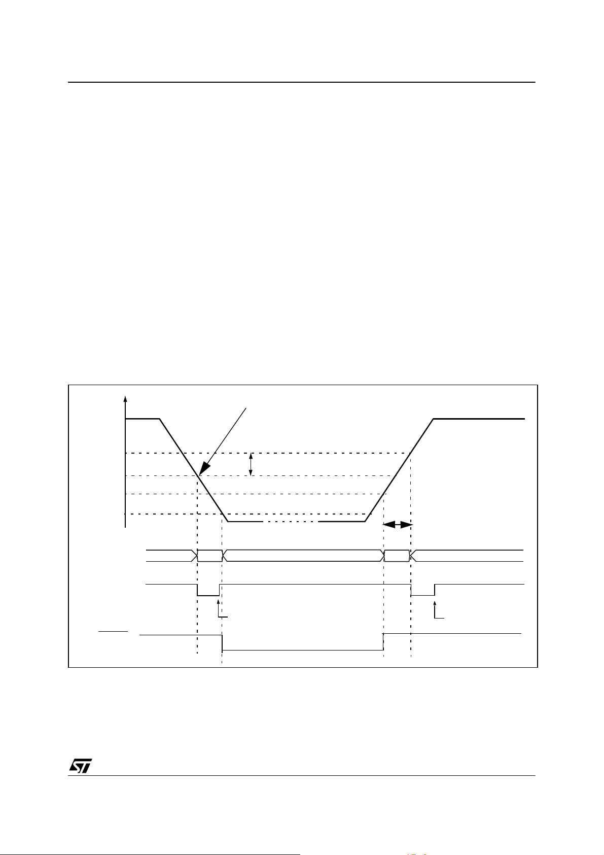
6.4.2.1 Monitoring the V
Main Su pply
DD
If the AVD interrupt is enabled, an interrupt is generated when the voltage crosses the V
V
IT-(AVD)
threshold (AVDF bit toggles).
IT+(AVD)
or
In the case of a drop in v oltage, th e A VD interrupt
acts as an early warning, allowing software to shut
ST72561
down safely before the LVD re sets the microcontroller. See Figure 16.
The interrupt on the rising edge is used to inform
the application that the V
If the voltage rise time t
CPU cycles (depending on the reset delay selected by option byte), no AVD interrupt will be generated when V
If t
is greater than 256 or 4096 cycles then:
rv
IT+(AVD)
is reached.
– If the AVD interrupt is enabled before the
V
IT+(AVD)
threshold is reached, then 2 AVD interrupts will be received: the first when the AVDIE
bit is set, and the second when the threshold is
reached.
– If the AVD interrupt is enabled after the V
threshold is reached then only one AVD interrupt
will occur.
warning state is over.
DD
is less than 256 or 4096
rv
IT+(AVD)
Figure 16. Using the AVD to Monitor V
V
DD
DD
Early Warning Interr upt
(Power has dropped, MCU not
not yet in reset)
V
V
IT+(AVD)
V
IT-(AVD)
V
IT+(LVD)
V
IT-(LVD)
AVDF bit 0 0RESET VALUE
AVD INTERRUPT
REQUEST
IF AVDIE bit = 1
LVD RESET
1
hyst
INTERRUPT PROCESS
t
VOLTAGE RISE TIME
rv
1
INTERRUPT PROCESS
27/262

ST72561
SYSTEM INTEGRITY MANAGEMENT (Cont’d)
6.4.3 Low Power Modes
Mode Description
WAIT
HALT The SICSR register is frozen.
6.4.3.1 Interrupts
The AVD interrupt event generates an interrupt if
the AVDIE bit is set and the interrupt mask in the
CC register is reset (RIM instructio n ).
No effect on SI. AVD interrupts cause the
device to exit from Wait mode.
Flag
Enable
Control
Bit
Interrupt Event
AVD event AVDF AVDIE Yes No
Event
Exit
from
Wait
Exit
from
Halt
28/262

SYSTEM INTEGRITY MANAGEMENT (Cont’d)
6.4.4 Register Description
SYSTEM INTEGRITY (SI) CONTROL/STATUS REGISTER (SICSR)
Read/Write
Reset Value: 000x 000x (00h)
Bits 3:1 = Reserved, must be kept cleared.
ST72561
70
AVD
IE
AVDFLVD
RF
000
0
WDG
RF
Bit 0 = WDGRF Watchdog reset flag
This bit indicates that the last Reset was generated by the Watchdog p eripheral. It is set by hardware (watchdog reset) and cleared by software
Bit 7 = Reserved, must be kept cleared.
(writing zero) or an LVD Reset (to ensure a stable
cleared state of the WDGRF flag when CPU
starts).
Bit 6 = AVDIE Voltage Detector interrupt enable
This bit is set and cleared by software. It enables
an interrupt to be generated when the AVDF flag
changes (toggles). The pending interrupt information is automatically cleared when software enters
the AVD interrupt routine.
0: AVD interrupt disabled
Combined with the LVDRF flag information, the
flag description is given by the following table.
RESET Sources LVDRF WDGRF
External RESET
Watchdog 0 1
LVD 1 X
pin 0 0
1: AVD interrupt enabled
Bit 5 = AVDF Voltage Detector flag
This read-only bit is set and cleared by hardware.
If the AVDIE bit is set, an interrupt request is generated when the AVDF bit changes value. Refer to
Figure 16 and to Section 6. 4.2.1 for additional de-
tails.
0: V
1: V
over V
DD
under V
DD
IT+(AVD)
IT-(AVD)
threshold
threshold
Application note s
The LVDRF flag is not cleared when another RESET type occurs (external or watchdog), the
LVDRF flag remains set to keep tra ce of the original failure.
In this case, a watchdog reset can be detected by
software while an external reset can not.
CAUTION: When the LVD is not activated with the
associated option byte, the WDGRF flag can not
Bit 4 = L VDRF LVD reset flag
be used in the application.
This bit indicates that the last Reset was generated by the LVD block. It is set by hardware (LVD reset) and cleared by software (writing zero). See
WDGRF flag description for more details. When
the LVD is disabled by OPTION BYTE, the LVDRF
bit value is undefined.
29/262

ST72561
7 INTERRUPTS
7.1 INTRODUCTION
The ST7 enhanced interrupt management provides the following features:
■ Hardware interrupts
■ Software interrupt (TRAP)
■ Nested or concurrent interrupt management
with flexible interrupt priority and level
management:
– Up to 4 software programmable nesting levels
– Up to 16 interrupt vectors fixed by hardware
– 2 non maskable events: RESET, TRAP
– 1 maskable Top Level Event: TLI
This interrupt management is based on:
– Bit 5 and bit 3 of the CPU CC register (I1:0),
– Interrupt software priority registers (ISPRx),
– Fixed interrupt vector addresses located at the
high addresses of the memory map (FFE0h to
FFFFh) sorted by hardware priority order.
This enhanced interrupt cont roller guarantees full
upward compatibility with the standard (not nested) ST7 interrupt controller.
7.2 MASKIN G AN D PROC ESSING FLOW
The interrupt masking is managed by the I1 and I0
bits of the CC register and the ISPRx registers
which give the interrupt software priority level of
each interrupt vector (see Table 6). The processing flow is shown in Figure 17
When an interrupt request has to be serviced:
– Normal processing is suspended at the end of
the current instruction execution.
– The PC, X, A and CC registers are saved onto
the stack.
– I1 and I0 bits of CC register are set according to
the corresponding values in the ISPRx registers
of the serviced interrupt vector.
– The PC is then loaded with the interrupt vector of
the interrupt to service and the first instruction of
the interrupt service routine is fetched (refer to
“Inter rupt M a pping ” table for vector addresses).
The interrupt service routine should end with the
IRET instruction which causes the contents of the
saved registers to be recovered from the stack.
Note: As a consequence of the IRET instruction,
the I1 and I0 bits will be rest ored from the stack
and the program in the previous level will resume.
Table 6. Interrupt Software Priority Levels
Interrupt software priority Level I1 I0
Level 0 (main) Low
Level 1 0 1
Level 2 0 0
Level 3 (= interrupt disable) 1 1
High
10
Figure 17. Int errupt Proces s in g Fl owchart
RESET
RESTORE PC, X, A, CC
FROM STACK
30/262
PENDING
INTERRUPT
N
FETCH NEX T
INSTRUCTION
Y
“IRET”
N
EXECUTE
INSTRUCTION
Y
THE INTERRUPT
STAYS PENDING
TLI
Interrupt has th e sam e or a
lower software priority
than current on e
STACK PC, X, A, CC
LOA D I1:0 FROM IN TERRUPT SW REG.
LOAD PC FROM INTERRUPT VECTOR
N
I1:0
software priority
than current one
Interrupt has a higher
Y
 Loading...