

8-bit MCU with up to 16 Kbytes Flash memory, 10-bit ADC,
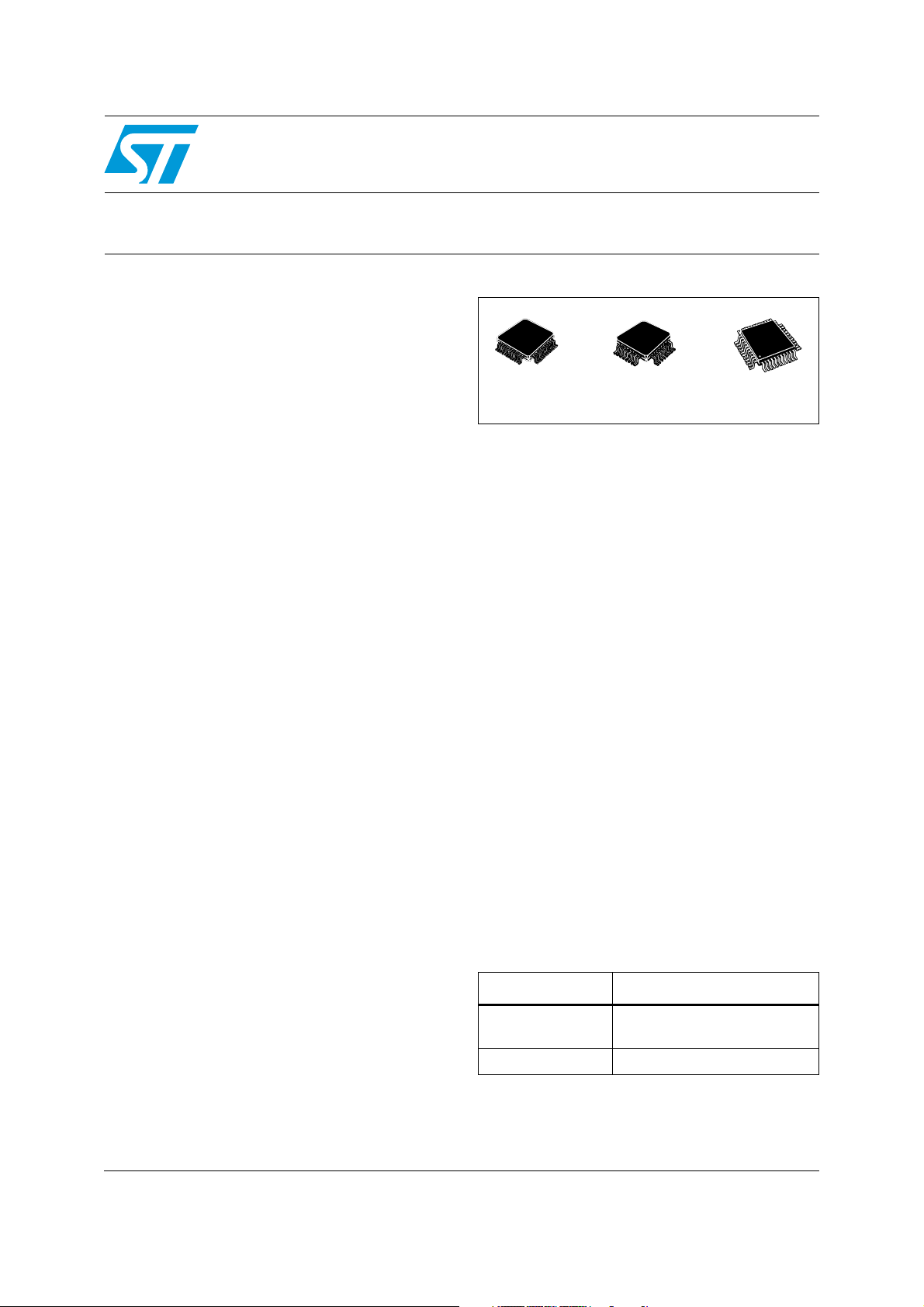
LQFP48
7 x 7 mm
LQFP44
LQFP32
7 × 7 mm
10 × 10 mm
Features
■ Memories
– up to 16 Kbytes Program memory: single
voltage extended Flash (XFlash) with readout and write protection, in-circuit and inapplication programming (ICP and IAP).
10,000 write/erase cycles guaranteed, data
retention: 20 years at 55 °C.
– up to 1 Kbyte RAM
– 256 bytes data EEPROM with readout
protection. 300,000 write/erase cycles
guaranteed, data retention: 20 years at
55 °C.
■ Clock, reset and supply management
– Power on / power off safe reset with
3 programmable threshold levels (LVD)
– Auxiliary voltage detector (AVD)
– Clock sources: crystal/ceramic resonator
oscillators, high-accuracy internal RC
oscillator or external clock
– PLL for 4x or 8x frequency multiplication
– 5 power-saving modes: Slow, Wait, Halt,
Auto-wakeup from Halt and Active-halt
– Clock output capability (f
■ Interrupt management
– Nested interrupt controller
– 10 interrupt vectors plus TRAP and RESET
– 9 external interrupt lines on 4 vectors
■ Up to 34 I/O ports
– up to 34 multifunctional bidirectional I/O
lines
– up to 12 high sink outputs (10 on 32-pin
devices)
■ 4 timers
– Configurable window watchdog timer
–Real-time base
– 16-bit timer A with: 1 input capture, 1 output
compare, external clock input, PWM and
pulse generator modes
CPU
)
ST72344xx, ST72345xx
two 16-bit timers, two I2C, SPI, SCI
Datasheet − production data
– 16-bit timer B with: 2 input captures, 2
output compares, PWM and pulse
generator modes
■ 3 communication interfaces
2
–I
C multimaster / slave
2
–I
C slave 3 addresses, no stretch, with
DMA access and byte pair coherency on
I²C read
– SCI asynchronous serial interface (LIN
compatible)
– SPI synchronous serial interface
■ 1 analog peripheral
– 10-bit ADC with 12 input channels (8 on 32-
pin devices)
■ Instruction set
– 8-bit data manipulation
– 63 basic instructions with illegal opcode
detection
– 17 main addressing modes
– 8 x 8 unsigned multiply instruction
■ Development tools
– Full hardware/software development
package
– On-chip debug module
Table 1. Device summary
References Part numbers
ST72344xx
ST72345xx ST72345C4
ST72344K2, ST72344K4,
ST72344S2, ST72344S4
July 2012 Doc ID 12321 Rev 6 1/247
This is information on a product in full production.
www.st.com
1

Contents ST72344xx, ST2345xx
Contents
1 Description . . . . . . . . . . . . . . . . . . . . . . . . . . . . . . . . . . . . . . . . . . . . . . . . 15
2 Pin description . . . . . . . . . . . . . . . . . . . . . . . . . . . . . . . . . . . . . . . . . . . . 17
3 Register and memory map . . . . . . . . . . . . . . . . . . . . . . . . . . . . . . . . . . . 23
4 Flash program memory . . . . . . . . . . . . . . . . . . . . . . . . . . . . . . . . . . . . . 27
4.1 Introduction . . . . . . . . . . . . . . . . . . . . . . . . . . . . . . . . . . . . . . . . . . . . . . . 27
4.2 Main features . . . . . . . . . . . . . . . . . . . . . . . . . . . . . . . . . . . . . . . . . . . . . . 27
4.3 Programming modes . . . . . . . . . . . . . . . . . . . . . . . . . . . . . . . . . . . . . . . . 27
4.3.1 In-circuit programming (ICP) . . . . . . . . . . . . . . . . . . . . . . . . . . . . . . . . . 28
4.3.2 In-application programming (IAP) . . . . . . . . . . . . . . . . . . . . . . . . . . . . . 28
4.4 ICC interface . . . . . . . . . . . . . . . . . . . . . . . . . . . . . . . . . . . . . . . . . . . . . . 28
4.5 Memory protection . . . . . . . . . . . . . . . . . . . . . . . . . . . . . . . . . . . . . . . . . . 29
4.5.1 Readout protection . . . . . . . . . . . . . . . . . . . . . . . . . . . . . . . . . . . . . . . . 29
4.5.2 Flash write/erase protection . . . . . . . . . . . . . . . . . . . . . . . . . . . . . . . . . . 30
4.6 Register description . . . . . . . . . . . . . . . . . . . . . . . . . . . . . . . . . . . . . . . . . 30
4.6.1 Flash control/status register (FCSR) . . . . . . . . . . . . . . . . . . . . . . . . . . . 30
5 Data EEPROM . . . . . . . . . . . . . . . . . . . . . . . . . . . . . . . . . . . . . . . . . . . . . 31
5.1 Introduction . . . . . . . . . . . . . . . . . . . . . . . . . . . . . . . . . . . . . . . . . . . . . . . 31
5.2 Main features . . . . . . . . . . . . . . . . . . . . . . . . . . . . . . . . . . . . . . . . . . . . . . 31
5.3 Memory access . . . . . . . . . . . . . . . . . . . . . . . . . . . . . . . . . . . . . . . . . . . . 31
5.4 Power saving modes . . . . . . . . . . . . . . . . . . . . . . . . . . . . . . . . . . . . . . . . 33
5.4.1 Wait mode . . . . . . . . . . . . . . . . . . . . . . . . . . . . . . . . . . . . . . . . . . . . . . . 33
5.4.2 Active-halt mode . . . . . . . . . . . . . . . . . . . . . . . . . . . . . . . . . . . . . . . . . . 33
5.4.3 Halt mode . . . . . . . . . . . . . . . . . . . . . . . . . . . . . . . . . . . . . . . . . . . . . . . 33
5.5 Access error handling . . . . . . . . . . . . . . . . . . . . . . . . . . . . . . . . . . . . . . . . 33
5.6 Data EEPROM readout protection . . . . . . . . . . . . . . . . . . . . . . . . . . . . . . 34
5.7 Register description . . . . . . . . . . . . . . . . . . . . . . . . . . . . . . . . . . . . . . . . . 35
5.7.1 EEPROM control/status register (EECSR) . . . . . . . . . . . . . . . . . . . . . . 35
6 Central processing unit . . . . . . . . . . . . . . . . . . . . . . . . . . . . . . . . . . . . . 36
2/247 Doc ID 12321 Rev 6

ST72344xx, ST2345xx Contents
6.1 Introduction . . . . . . . . . . . . . . . . . . . . . . . . . . . . . . . . . . . . . . . . . . . . . . . 36
6.2 Main features . . . . . . . . . . . . . . . . . . . . . . . . . . . . . . . . . . . . . . . . . . . . . . 36
6.3 CPU registers . . . . . . . . . . . . . . . . . . . . . . . . . . . . . . . . . . . . . . . . . . . . . . 36
6.3.1 Condition code register (CC) . . . . . . . . . . . . . . . . . . . . . . . . . . . . . . . . . 37
6.3.2 Stack pointer (SP) . . . . . . . . . . . . . . . . . . . . . . . . . . . . . . . . . . . . . . . . . 39
7 Supply, reset and clock management . . . . . . . . . . . . . . . . . . . . . . . . . . 41
7.1 Main features . . . . . . . . . . . . . . . . . . . . . . . . . . . . . . . . . . . . . . . . . . . . . . 41
7.2 Phase locked loop . . . . . . . . . . . . . . . . . . . . . . . . . . . . . . . . . . . . . . . . . . 42
7.3 Multioscillator (MO) . . . . . . . . . . . . . . . . . . . . . . . . . . . . . . . . . . . . . . . . . 43
7.3.1 External clock source . . . . . . . . . . . . . . . . . . . . . . . . . . . . . . . . . . . . . . . 43
7.3.2 Crystal/ceramic oscillators . . . . . . . . . . . . . . . . . . . . . . . . . . . . . . . . . . . 43
7.3.3 Internal RC oscillator . . . . . . . . . . . . . . . . . . . . . . . . . . . . . . . . . . . . . . . 45
7.4 Register description . . . . . . . . . . . . . . . . . . . . . . . . . . . . . . . . . . . . . . . . . 45
7.4.1 RC control register (RCCRH) . . . . . . . . . . . . . . . . . . . . . . . . . . . . . . . . 45
7.4.2 RC control register (RCCRL) . . . . . . . . . . . . . . . . . . . . . . . . . . . . . . . . . 46
7.5 Reset sequence manager (RSM) . . . . . . . . . . . . . . . . . . . . . . . . . . . . . . . 46
7.5.1 Introduction . . . . . . . . . . . . . . . . . . . . . . . . . . . . . . . . . . . . . . . . . . . . . . 46
7.5.2 Asynchronous external RESET pin . . . . . . . . . . . . . . . . . . . . . . . . . . . . 47
7.5.3 External power-on reset . . . . . . . . . . . . . . . . . . . . . . . . . . . . . . . . . . . . . 47
7.5.4 Internal low-voltage detector (LVD) reset . . . . . . . . . . . . . . . . . . . . . . . . 48
7.5.5 Internal watchdog reset . . . . . . . . . . . . . . . . . . . . . . . . . . . . . . . . . . . . . 48
7.6 System integrity management (SI) . . . . . . . . . . . . . . . . . . . . . . . . . . . . . . 48
7.6.1 Low-voltage detector (LVD) . . . . . . . . . . . . . . . . . . . . . . . . . . . . . . . . . . 49
7.6.2 Auxiliary-voltage detector (AVD) . . . . . . . . . . . . . . . . . . . . . . . . . . . . . . 49
7.6.3 Low-power modes . . . . . . . . . . . . . . . . . . . . . . . . . . . . . . . . . . . . . . . . . 50
7.6.4 Interrupts . . . . . . . . . . . . . . . . . . . . . . . . . . . . . . . . . . . . . . . . . . . . . . . . 50
7.6.5 Register description . . . . . . . . . . . . . . . . . . . . . . . . . . . . . . . . . . . . . . . . 51
8 Interrupts . . . . . . . . . . . . . . . . . . . . . . . . . . . . . . . . . . . . . . . . . . . . . . . . . 53
8.1 Introduction . . . . . . . . . . . . . . . . . . . . . . . . . . . . . . . . . . . . . . . . . . . . . . . 53
8.2 Masking and processing flow . . . . . . . . . . . . . . . . . . . . . . . . . . . . . . . . . . 53
8.3 Interrupts and low-power modes . . . . . . . . . . . . . . . . . . . . . . . . . . . . . . . 56
8.4 Concurrent & nested management . . . . . . . . . . . . . . . . . . . . . . . . . . . . . 56
8.5 Interrupt register description . . . . . . . . . . . . . . . . . . . . . . . . . . . . . . . . . . 57
8.5.1 CPU CC register interrupt bits . . . . . . . . . . . . . . . . . . . . . . . . . . . . . . . . 57
Doc ID 12321 Rev 6 3/247

Contents ST72344xx, ST2345xx
8.5.2 Interrupt software priority registers (ISPRX) . . . . . . . . . . . . . . . . . . . . . 58
8.6 External interrupts . . . . . . . . . . . . . . . . . . . . . . . . . . . . . . . . . . . . . . . . . . 60
8.6.1 I/O port interrupt sensitivity . . . . . . . . . . . . . . . . . . . . . . . . . . . . . . . . . . 60
8.7 External interrupt control register (EICR) . . . . . . . . . . . . . . . . . . . . . . . . . 61
9 Power-saving modes . . . . . . . . . . . . . . . . . . . . . . . . . . . . . . . . . . . . . . . . 64
9.1 Introduction . . . . . . . . . . . . . . . . . . . . . . . . . . . . . . . . . . . . . . . . . . . . . . . 64
9.2 Slow mode . . . . . . . . . . . . . . . . . . . . . . . . . . . . . . . . . . . . . . . . . . . . . . . . 65
9.3 Wait mode . . . . . . . . . . . . . . . . . . . . . . . . . . . . . . . . . . . . . . . . . . . . . . . . 65
9.4 Halt mode . . . . . . . . . . . . . . . . . . . . . . . . . . . . . . . . . . . . . . . . . . . . . . . . . 66
9.5 Active-halt mode . . . . . . . . . . . . . . . . . . . . . . . . . . . . . . . . . . . . . . . . . . . . 68
9.6 Auto-wakeup from Halt mode . . . . . . . . . . . . . . . . . . . . . . . . . . . . . . . . . . 70
9.7 Register description . . . . . . . . . . . . . . . . . . . . . . . . . . . . . . . . . . . . . . . . . 72
9.7.1 AWUFH control/status register (AWUCSR) . . . . . . . . . . . . . . . . . . . . . . 72
9.7.2 AWUFH prescaler register (AWUPR) . . . . . . . . . . . . . . . . . . . . . . . . . . 73
10 I/O ports . . . . . . . . . . . . . . . . . . . . . . . . . . . . . . . . . . . . . . . . . . . . . . . . . . 74
10.1 Introduction . . . . . . . . . . . . . . . . . . . . . . . . . . . . . . . . . . . . . . . . . . . . . . . 74
10.2 Functional description . . . . . . . . . . . . . . . . . . . . . . . . . . . . . . . . . . . . . . . 74
10.2.1 Input modes . . . . . . . . . . . . . . . . . . . . . . . . . . . . . . . . . . . . . . . . . . . . . . 74
10.2.2 Output modes . . . . . . . . . . . . . . . . . . . . . . . . . . . . . . . . . . . . . . . . . . . . 75
10.2.3 Alternate functions . . . . . . . . . . . . . . . . . . . . . . . . . . . . . . . . . . . . . . . . . 75
10.3 I/O port implementation . . . . . . . . . . . . . . . . . . . . . . . . . . . . . . . . . . . . . . 78
10.4 Low-power modes . . . . . . . . . . . . . . . . . . . . . . . . . . . . . . . . . . . . . . . . . . 78
10.5 Interrupts . . . . . . . . . . . . . . . . . . . . . . . . . . . . . . . . . . . . . . . . . . . . . . . . . 78
10.5.1 I/O port implementation . . . . . . . . . . . . . . . . . . . . . . . . . . . . . . . . . . . . . 79
11 On-chip peripherals . . . . . . . . . . . . . . . . . . . . . . . . . . . . . . . . . . . . . . . . 82
11.1 Window watchdog (WWDG) . . . . . . . . . . . . . . . . . . . . . . . . . . . . . . . . . . . 82
11.1.1 Introduction . . . . . . . . . . . . . . . . . . . . . . . . . . . . . . . . . . . . . . . . . . . . . . 82
11.1.2 Main features . . . . . . . . . . . . . . . . . . . . . . . . . . . . . . . . . . . . . . . . . . . . . 82
11.1.3 Functional description . . . . . . . . . . . . . . . . . . . . . . . . . . . . . . . . . . . . . . 82
11.1.4 Using Halt mode with the WDG . . . . . . . . . . . . . . . . . . . . . . . . . . . . . . . 84
11.1.5 How to program the watchdog timeout . . . . . . . . . . . . . . . . . . . . . . . . . 84
11.1.6 Low-power modes . . . . . . . . . . . . . . . . . . . . . . . . . . . . . . . . . . . . . . . . . 86
11.1.7 Hardware watchdog option . . . . . . . . . . . . . . . . . . . . . . . . . . . . . . . . . . 87
4/247 Doc ID 12321 Rev 6

ST72344xx, ST2345xx Contents
11.1.8 Using Halt mode with the WDG (WDGHALT option) . . . . . . . . . . . . . . . 87
11.1.9 Interrupts . . . . . . . . . . . . . . . . . . . . . . . . . . . . . . . . . . . . . . . . . . . . . . . . 87
11.1.10 Register description . . . . . . . . . . . . . . . . . . . . . . . . . . . . . . . . . . . . . . . . 87
11.2 Main clock controller with real-time clock and beeper (MCC/RTC) . . . . . 88
11.2.1 Programmable CPU clock prescaler . . . . . . . . . . . . . . . . . . . . . . . . . . . 88
11.2.2 Clock-out capability . . . . . . . . . . . . . . . . . . . . . . . . . . . . . . . . . . . . . . . . 88
11.2.3 Real-time clock timer (RTC) . . . . . . . . . . . . . . . . . . . . . . . . . . . . . . . . . . 88
11.2.4 Beeper . . . . . . . . . . . . . . . . . . . . . . . . . . . . . . . . . . . . . . . . . . . . . . . . . . 88
11.2.5 Low-power modes . . . . . . . . . . . . . . . . . . . . . . . . . . . . . . . . . . . . . . . . . 89
11.2.6 Interrupts . . . . . . . . . . . . . . . . . . . . . . . . . . . . . . . . . . . . . . . . . . . . . . . . 89
11.2.7 Register description . . . . . . . . . . . . . . . . . . . . . . . . . . . . . . . . . . . . . . . . 90
11.3 16-bit timer . . . . . . . . . . . . . . . . . . . . . . . . . . . . . . . . . . . . . . . . . . . . . . . . 93
11.3.1 Introduction . . . . . . . . . . . . . . . . . . . . . . . . . . . . . . . . . . . . . . . . . . . . . . 93
11.3.2 Main features . . . . . . . . . . . . . . . . . . . . . . . . . . . . . . . . . . . . . . . . . . . . . 93
11.3.3 Functional description . . . . . . . . . . . . . . . . . . . . . . . . . . . . . . . . . . . . . . 94
11.3.4 Low-power modes . . . . . . . . . . . . . . . . . . . . . . . . . . . . . . . . . . . . . . . . 107
11.3.5 Interrupts . . . . . . . . . . . . . . . . . . . . . . . . . . . . . . . . . . . . . . . . . . . . . . . 107
11.3.6 Summary of timer modes . . . . . . . . . . . . . . . . . . . . . . . . . . . . . . . . . . . 108
11.3.7 Register description . . . . . . . . . . . . . . . . . . . . . . . . . . . . . . . . . . . . . . . 108
11.4 Serial peripheral interface (SPI) . . . . . . . . . . . . . . . . . . . . . . . . . . . . . . . 115
11.4.1 Introduction . . . . . . . . . . . . . . . . . . . . . . . . . . . . . . . . . . . . . . . . . . . . . 115
11.4.2 Main features . . . . . . . . . . . . . . . . . . . . . . . . . . . . . . . . . . . . . . . . . . . . 115
11.4.3 General description . . . . . . . . . . . . . . . . . . . . . . . . . . . . . . . . . . . . . . . 115
11.4.4 Clock phase and clock polarity . . . . . . . . . . . . . . . . . . . . . . . . . . . . . . 120
11.4.5 Error flags . . . . . . . . . . . . . . . . . . . . . . . . . . . . . . . . . . . . . . . . . . . . . . 121
11.4.6 Low-power modes . . . . . . . . . . . . . . . . . . . . . . . . . . . . . . . . . . . . . . . . 124
11.4.7 Interrupts . . . . . . . . . . . . . . . . . . . . . . . . . . . . . . . . . . . . . . . . . . . . . . . 125
11.4.8 Register description . . . . . . . . . . . . . . . . . . . . . . . . . . . . . . . . . . . . . . . 125
11.5 SCI serial communication interface . . . . . . . . . . . . . . . . . . . . . . . . . . . . 129
11.5.1 Introduction . . . . . . . . . . . . . . . . . . . . . . . . . . . . . . . . . . . . . . . . . . . . . 129
11.5.2 Main features . . . . . . . . . . . . . . . . . . . . . . . . . . . . . . . . . . . . . . . . . . . . 129
11.5.3 General description . . . . . . . . . . . . . . . . . . . . . . . . . . . . . . . . . . . . . . . 129
11.5.4 Functional description . . . . . . . . . . . . . . . . . . . . . . . . . . . . . . . . . . . . . 132
11.5.5 Low-power modes . . . . . . . . . . . . . . . . . . . . . . . . . . . . . . . . . . . . . . . . 141
11.5.6 Interrupts . . . . . . . . . . . . . . . . . . . . . . . . . . . . . . . . . . . . . . . . . . . . . . . 142
11.5.7 Register description . . . . . . . . . . . . . . . . . . . . . . . . . . . . . . . . . . . . . . . 142
Doc ID 12321 Rev 6 5/247

Contents ST72344xx, ST2345xx
11.6 I2C bus interface (I2C) . . . . . . . . . . . . . . . . . . . . . . . . . . . . . . . . . . . . . . 150
11.6.1 Introduction . . . . . . . . . . . . . . . . . . . . . . . . . . . . . . . . . . . . . . . . . . . . . 150
11.6.2 Main features . . . . . . . . . . . . . . . . . . . . . . . . . . . . . . . . . . . . . . . . . . . . 150
11.6.3 General description . . . . . . . . . . . . . . . . . . . . . . . . . . . . . . . . . . . . . . . 150
11.6.4 Functional description . . . . . . . . . . . . . . . . . . . . . . . . . . . . . . . . . . . . . 152
11.6.5 Low-power modes . . . . . . . . . . . . . . . . . . . . . . . . . . . . . . . . . . . . . . . . 158
11.6.6 Interrupts . . . . . . . . . . . . . . . . . . . . . . . . . . . . . . . . . . . . . . . . . . . . . . . 158
11.6.7 Register description . . . . . . . . . . . . . . . . . . . . . . . . . . . . . . . . . . . . . . . 159
11.7 I2C triple slave interface with DMA (I2C3S) . . . . . . . . . . . . . . . . . . . . . . 167
11.7.1 Introduction . . . . . . . . . . . . . . . . . . . . . . . . . . . . . . . . . . . . . . . . . . . . . 167
11.7.2 Main features . . . . . . . . . . . . . . . . . . . . . . . . . . . . . . . . . . . . . . . . . . . . 167
11.7.3 General description . . . . . . . . . . . . . . . . . . . . . . . . . . . . . . . . . . . . . . . 168
11.7.4 Functional description . . . . . . . . . . . . . . . . . . . . . . . . . . . . . . . . . . . . . 169
11.7.5 Address handling . . . . . . . . . . . . . . . . . . . . . . . . . . . . . . . . . . . . . . . . . 172
11.7.6 Low-power modes . . . . . . . . . . . . . . . . . . . . . . . . . . . . . . . . . . . . . . . . 176
11.7.7 Interrupt generation . . . . . . . . . . . . . . . . . . . . . . . . . . . . . . . . . . . . . . . 177
11.7.8 Register description . . . . . . . . . . . . . . . . . . . . . . . . . . . . . . . . . . . . . . . 178
11.8 10-bit A/D converter (ADC) . . . . . . . . . . . . . . . . . . . . . . . . . . . . . . . . . . 185
11.8.1 Introduction . . . . . . . . . . . . . . . . . . . . . . . . . . . . . . . . . . . . . . . . . . . . . 185
11.8.2 Main features . . . . . . . . . . . . . . . . . . . . . . . . . . . . . . . . . . . . . . . . . . . . 185
11.8.3 Functional description . . . . . . . . . . . . . . . . . . . . . . . . . . . . . . . . . . . . . 186
11.8.4 Low-power modes . . . . . . . . . . . . . . . . . . . . . . . . . . . . . . . . . . . . . . . . 187
11.8.5 Interrupts . . . . . . . . . . . . . . . . . . . . . . . . . . . . . . . . . . . . . . . . . . . . . . . 187
11.8.6 Register description . . . . . . . . . . . . . . . . . . . . . . . . . . . . . . . . . . . . . . . 187
12 Instruction set . . . . . . . . . . . . . . . . . . . . . . . . . . . . . . . . . . . . . . . . . . . . 190
12.1 ST7 addressing modes . . . . . . . . . . . . . . . . . . . . . . . . . . . . . . . . . . . . . 190
12.1.1 Inherent . . . . . . . . . . . . . . . . . . . . . . . . . . . . . . . . . . . . . . . . . . . . . . . . 191
12.1.2 Immediate . . . . . . . . . . . . . . . . . . . . . . . . . . . . . . . . . . . . . . . . . . . . . . 192
12.1.3 Direct . . . . . . . . . . . . . . . . . . . . . . . . . . . . . . . . . . . . . . . . . . . . . . . . . . 192
12.1.4 Indexed (No Offset, Short, Long) . . . . . . . . . . . . . . . . . . . . . . . . . . . . . 192
12.1.5 Indirect (Short, Long) . . . . . . . . . . . . . . . . . . . . . . . . . . . . . . . . . . . . . . 193
12.1.6 Indirect Indexed (Short, Long) . . . . . . . . . . . . . . . . . . . . . . . . . . . . . . . 193
12.1.7 Relative Mode (direct, indirect) . . . . . . . . . . . . . . . . . . . . . . . . . . . . . . 194
12.2 Instruction groups . . . . . . . . . . . . . . . . . . . . . . . . . . . . . . . . . . . . . . . . . . 195
12.2.1 Illegal opcode reset . . . . . . . . . . . . . . . . . . . . . . . . . . . . . . . . . . . . . . . 196
6/247 Doc ID 12321 Rev 6

ST72344xx, ST2345xx Contents
13 Electrical characteristics . . . . . . . . . . . . . . . . . . . . . . . . . . . . . . . . . . . 199
13.1 Parameter conditions . . . . . . . . . . . . . . . . . . . . . . . . . . . . . . . . . . . . . . . 199
13.1.1 Minimum and maximum values . . . . . . . . . . . . . . . . . . . . . . . . . . . . . . 199
13.1.2 Typical values . . . . . . . . . . . . . . . . . . . . . . . . . . . . . . . . . . . . . . . . . . . . 199
13.1.3 Typical curves . . . . . . . . . . . . . . . . . . . . . . . . . . . . . . . . . . . . . . . . . . . 199
13.1.4 Loading capacitor . . . . . . . . . . . . . . . . . . . . . . . . . . . . . . . . . . . . . . . . 199
13.1.5 Pin input voltage . . . . . . . . . . . . . . . . . . . . . . . . . . . . . . . . . . . . . . . . . 200
13.2 Absolute maximum ratings . . . . . . . . . . . . . . . . . . . . . . . . . . . . . . . . . . . 200
13.3 Operating conditions . . . . . . . . . . . . . . . . . . . . . . . . . . . . . . . . . . . . . . . 202
13.4 Internal RC oscillator characteristics . . . . . . . . . . . . . . . . . . . . . . . . . . . 204
13.5 Supply current characteristics . . . . . . . . . . . . . . . . . . . . . . . . . . . . . . . . 205
13.6 Clock and timing characteristics . . . . . . . . . . . . . . . . . . . . . . . . . . . . . . . 209
13.6.1 Crystal and ceramic resonator oscillators . . . . . . . . . . . . . . . . . . . . . . 210
13.7 Memory characteristics . . . . . . . . . . . . . . . . . . . . . . . . . . . . . . . . . . . . . 212
13.8 EMC characteristics . . . . . . . . . . . . . . . . . . . . . . . . . . . . . . . . . . . . . . . . 213
13.8.1 Functional EMS (electromagnetic susceptibility) . . . . . . . . . . . . . . . . . 213
13.8.2 EMI (electromagnetic interference) . . . . . . . . . . . . . . . . . . . . . . . . . . . 214
13.8.3 Absolute maximum ratings (electrical sensitivity) . . . . . . . . . . . . . . . . 214
13.9 I/O port pin characteristics . . . . . . . . . . . . . . . . . . . . . . . . . . . . . . . . . . . 215
13.10 Control pin characteristics . . . . . . . . . . . . . . . . . . . . . . . . . . . . . . . . . . . 222
13.10.1 Asynchronous RESET pin . . . . . . . . . . . . . . . . . . . . . . . . . . . . . . . . . . 222
13.11 Communication interface characteristics . . . . . . . . . . . . . . . . . . . . . . . . 224
13.11.1 I2C and I²C3SNS interfaces . . . . . . . . . . . . . . . . . . . . . . . . . . . . . . . . . 224
13.12 10-bit ADC characteristics . . . . . . . . . . . . . . . . . . . . . . . . . . . . . . . . . . . 225
14 Package characteristics . . . . . . . . . . . . . . . . . . . . . . . . . . . . . . . . . . . . 227
14.1 ECOPACK . . . . . . . . . . . . . . . . . . . . . . . . . . . . . . . . . . . . . . . . . . . . . . . 227
14.2 Package mechanical data . . . . . . . . . . . . . . . . . . . . . . . . . . . . . . . . . . . 227
15 Device configuration and ordering information . . . . . . . . . . . . . . . . . 232
15.1 Option bytes . . . . . . . . . . . . . . . . . . . . . . . . . . . . . . . . . . . . . . . . . . . . . . 232
15.1.1 Option byte 0 . . . . . . . . . . . . . . . . . . . . . . . . . . . . . . . . . . . . . . . . . . . . 232
15.1.2 Option byte 1 . . . . . . . . . . . . . . . . . . . . . . . . . . . . . . . . . . . . . . . . . . . . 233
15.1.3 Option byte 2 . . . . . . . . . . . . . . . . . . . . . . . . . . . . . . . . . . . . . . . . . . . . 234
15.1.4 Option byte 3 . . . . . . . . . . . . . . . . . . . . . . . . . . . . . . . . . . . . . . . . . . . . 235
Doc ID 12321 Rev 6 7/247

Contents ST72344xx, ST2345xx
15.2 Device ordering information . . . . . . . . . . . . . . . . . . . . . . . . . . . . . . . . . . 236
15.3 Development tools . . . . . . . . . . . . . . . . . . . . . . . . . . . . . . . . . . . . . . . . . 236
15.3.1 Starter kits . . . . . . . . . . . . . . . . . . . . . . . . . . . . . . . . . . . . . . . . . . . . . . 236
15.3.2 Development and debugging tools . . . . . . . . . . . . . . . . . . . . . . . . . . . 237
15.3.3 Programming tools . . . . . . . . . . . . . . . . . . . . . . . . . . . . . . . . . . . . . . . . 237
15.3.4 Order codes for ST72F34x development tools . . . . . . . . . . . . . . . . . . 238
16 Known limitations . . . . . . . . . . . . . . . . . . . . . . . . . . . . . . . . . . . . . . . . . 239
16.1 External interrupt missed . . . . . . . . . . . . . . . . . . . . . . . . . . . . . . . . . . . . 239
16.1.1 Workaround . . . . . . . . . . . . . . . . . . . . . . . . . . . . . . . . . . . . . . . . . . . . . 239
16.1.2 Unexpected reset fetch . . . . . . . . . . . . . . . . . . . . . . . . . . . . . . . . . . . . 241
16.2 Clearing active interrupts outside interrupt routine . . . . . . . . . . . . . . . . . 241
16.3 16-bit timer PWM mode . . . . . . . . . . . . . . . . . . . . . . . . . . . . . . . . . . . . . 242
16.4 TIMD set simultaneously with OC interrupt . . . . . . . . . . . . . . . . . . . . . . 242
16.4.1 Impact on the application . . . . . . . . . . . . . . . . . . . . . . . . . . . . . . . . . . . 242
16.4.2 Workaround . . . . . . . . . . . . . . . . . . . . . . . . . . . . . . . . . . . . . . . . . . . . . 242
16.5 SCI wrong break duration . . . . . . . . . . . . . . . . . . . . . . . . . . . . . . . . . . . . 242
16.5.1 Description . . . . . . . . . . . . . . . . . . . . . . . . . . . . . . . . . . . . . . . . . . . . . . 242
16.5.2 Occurrence . . . . . . . . . . . . . . . . . . . . . . . . . . . . . . . . . . . . . . . . . . . . . 243
16.5.3 Workaround . . . . . . . . . . . . . . . . . . . . . . . . . . . . . . . . . . . . . . . . . . . . . 243
16.6 Random read operations not supported with the standard I²C . . . . . . . 243
16.6.1 Description . . . . . . . . . . . . . . . . . . . . . . . . . . . . . . . . . . . . . . . . . . . . . . 243
16.6.2 Occurrence . . . . . . . . . . . . . . . . . . . . . . . . . . . . . . . . . . . . . . . . . . . . . 243
16.6.3 Workaround . . . . . . . . . . . . . . . . . . . . . . . . . . . . . . . . . . . . . . . . . . . . . 243
16.7 Programming of EEPROM data . . . . . . . . . . . . . . . . . . . . . . . . . . . . . . . 243
16.7.1 Description . . . . . . . . . . . . . . . . . . . . . . . . . . . . . . . . . . . . . . . . . . . . . . 243
16.7.2 Impact on application . . . . . . . . . . . . . . . . . . . . . . . . . . . . . . . . . . . . . . 243
16.7.3 Workaround . . . . . . . . . . . . . . . . . . . . . . . . . . . . . . . . . . . . . . . . . . . . . 244
17 Revision history . . . . . . . . . . . . . . . . . . . . . . . . . . . . . . . . . . . . . . . . . . 245
8/247 Doc ID 12321 Rev 6

ST72344xx, ST2345xx List of tables
List of tables
Table 1. Device summary . . . . . . . . . . . . . . . . . . . . . . . . . . . . . . . . . . . . . . . . . . . . . . . . . . . . . . . . . . 1
Table 2. ST72344xx and ST72345xx features . . . . . . . . . . . . . . . . . . . . . . . . . . . . . . . . . . . . . . . . . 16
Table 3. Device pin description. . . . . . . . . . . . . . . . . . . . . . . . . . . . . . . . . . . . . . . . . . . . . . . . . . . . . 20
Table 4. Hardware register map . . . . . . . . . . . . . . . . . . . . . . . . . . . . . . . . . . . . . . . . . . . . . . . . . . . . 24
Table 5. Data EEPROM register map and reset values . . . . . . . . . . . . . . . . . . . . . . . . . . . . . . . . . . 35
Table 6. Interrupt software priority . . . . . . . . . . . . . . . . . . . . . . . . . . . . . . . . . . . . . . . . . . . . . . . . . . 38
Table 7. PLL configurations . . . . . . . . . . . . . . . . . . . . . . . . . . . . . . . . . . . . . . . . . . . . . . . . . . . . . . . 42
Table 8. ST7 clock sources . . . . . . . . . . . . . . . . . . . . . . . . . . . . . . . . . . . . . . . . . . . . . . . . . . . . . . . 44
Table 9. Calibration values . . . . . . . . . . . . . . . . . . . . . . . . . . . . . . . . . . . . . . . . . . . . . . . . . . . . . . . . 45
Table 10. Low-power mode description . . . . . . . . . . . . . . . . . . . . . . . . . . . . . . . . . . . . . . . . . . . . . . . 50
Table 11. Interrupt event. . . . . . . . . . . . . . . . . . . . . . . . . . . . . . . . . . . . . . . . . . . . . . . . . . . . . . . . . . . 50
Table 12. LVDRF and WDGRF description . . . . . . . . . . . . . . . . . . . . . . . . . . . . . . . . . . . . . . . . . . . . 51
Table 13. Interrupt software priority levels . . . . . . . . . . . . . . . . . . . . . . . . . . . . . . . . . . . . . . . . . . . . . 54
Table 14. Interrupt software priority . . . . . . . . . . . . . . . . . . . . . . . . . . . . . . . . . . . . . . . . . . . . . . . . . . 57
Table 15. Interrupt vector addresses . . . . . . . . . . . . . . . . . . . . . . . . . . . . . . . . . . . . . . . . . . . . . . . . . 58
Table 16. Dedicated interrupt instruction set . . . . . . . . . . . . . . . . . . . . . . . . . . . . . . . . . . . . . . . . . . . 58
Table 17. Interrupt mapping . . . . . . . . . . . . . . . . . . . . . . . . . . . . . . . . . . . . . . . . . . . . . . . . . . . . . . . . 59
Table 18. External interrupt sensitivity (ei2) . . . . . . . . . . . . . . . . . . . . . . . . . . . . . . . . . . . . . . . . . . . . 61
Table 19. External interrupt sensitivity (ei3) . . . . . . . . . . . . . . . . . . . . . . . . . . . . . . . . . . . . . . . . . . . . 61
Table 20. External interrupt sensitivity (ei0) . . . . . . . . . . . . . . . . . . . . . . . . . . . . . . . . . . . . . . . . . . . . 62
Table 21. External interrupt sensitivity (ei1) . . . . . . . . . . . . . . . . . . . . . . . . . . . . . . . . . . . . . . . . . . . . 62
Table 22. Nested interrupts register map and reset values . . . . . . . . . . . . . . . . . . . . . . . . . . . . . . . . 63
Table 23. Power saving mode . . . . . . . . . . . . . . . . . . . . . . . . . . . . . . . . . . . . . . . . . . . . . . . . . . . . . . 68
Table 24. AWUPR dividing factor . . . . . . . . . . . . . . . . . . . . . . . . . . . . . . . . . . . . . . . . . . . . . . . . . . . . 73
Table 25. AWU register map and reset values . . . . . . . . . . . . . . . . . . . . . . . . . . . . . . . . . . . . . . . . . . 73
Table 26. Output modes . . . . . . . . . . . . . . . . . . . . . . . . . . . . . . . . . . . . . . . . . . . . . . . . . . . . . . . . . . . 75
Table 27. I/O Port mode options. . . . . . . . . . . . . . . . . . . . . . . . . . . . . . . . . . . . . . . . . . . . . . . . . . . . . 76
Table 28. I/O port configurations . . . . . . . . . . . . . . . . . . . . . . . . . . . . . . . . . . . . . . . . . . . . . . . . . . . . 77
Table 29. Description . . . . . . . . . . . . . . . . . . . . . . . . . . . . . . . . . . . . . . . . . . . . . . . . . . . . . . . . . . . . . 78
Table 30. Description of interrupt events . . . . . . . . . . . . . . . . . . . . . . . . . . . . . . . . . . . . . . . . . . . . . . 78
Table 31. I/O port register configurations (standard ports) . . . . . . . . . . . . . . . . . . . . . . . . . . . . . . . . . 79
Table 32. I/O port register configurations (interrupt ports with pull-up). . . . . . . . . . . . . . . . . . . . . . . . 79
Table 33. I/O port register configurations (interrupt ports without pull-up) . . . . . . . . . . . . . . . . . . . . . 79
Table 34. I/O port register configurations (true open drain ports) . . . . . . . . . . . . . . . . . . . . . . . . . . . . 79
Table 35. Port configuration . . . . . . . . . . . . . . . . . . . . . . . . . . . . . . . . . . . . . . . . . . . . . . . . . . . . . . . . 80
Table 36. I/O port register map and reset values . . . . . . . . . . . . . . . . . . . . . . . . . . . . . . . . . . . . . . . . 80
Table 37. Descriptions . . . . . . . . . . . . . . . . . . . . . . . . . . . . . . . . . . . . . . . . . . . . . . . . . . . . . . . . . . . . 86
Table 38. Watchdog timer register map and reset values . . . . . . . . . . . . . . . . . . . . . . . . . . . . . . . . . 88
Table 39. Mode description . . . . . . . . . . . . . . . . . . . . . . . . . . . . . . . . . . . . . . . . . . . . . . . . . . . . . . . . 89
Table 40. Interrupt event. . . . . . . . . . . . . . . . . . . . . . . . . . . . . . . . . . . . . . . . . . . . . . . . . . . . . . . . . . . 89
Table 41. CPU clock prescaler selection . . . . . . . . . . . . . . . . . . . . . . . . . . . . . . . . . . . . . . . . . . . . . . 90
Table 42. Time base control . . . . . . . . . . . . . . . . . . . . . . . . . . . . . . . . . . . . . . . . . . . . . . . . . . . . . . . . 91
Table 43. Beep control . . . . . . . . . . . . . . . . . . . . . . . . . . . . . . . . . . . . . . . . . . . . . . . . . . . . . . . . . . . . 92
Table 44. Main clock controller register map and reset values. . . . . . . . . . . . . . . . . . . . . . . . . . . . . . 92
Table 45. ICiR register . . . . . . . . . . . . . . . . . . . . . . . . . . . . . . . . . . . . . . . . . . . . . . . . . . . . . . . . . . . . 98
Table 46. OCiR register . . . . . . . . . . . . . . . . . . . . . . . . . . . . . . . . . . . . . . . . . . . . . . . . . . . . . . . . . . 100
Table 47. Low-power mode description . . . . . . . . . . . . . . . . . . . . . . . . . . . . . . . . . . . . . . . . . . . . . . 107
Table 48. Interrupt events. . . . . . . . . . . . . . . . . . . . . . . . . . . . . . . . . . . . . . . . . . . . . . . . . . . . . . . . . 107
Doc ID 12321 Rev 6 9/247

List of tables ST72344xx, ST2345xx
Table 49. Timer modes . . . . . . . . . . . . . . . . . . . . . . . . . . . . . . . . . . . . . . . . . . . . . . . . . . . . . . . . . . . 108
Table 50. Clock control bits . . . . . . . . . . . . . . . . . . . . . . . . . . . . . . . . . . . . . . . . . . . . . . . . . . . . . . . 110
Table 51. 16-bit timer register map and reset values . . . . . . . . . . . . . . . . . . . . . . . . . . . . . . . . . . . . 114
Table 52. Description . . . . . . . . . . . . . . . . . . . . . . . . . . . . . . . . . . . . . . . . . . . . . . . . . . . . . . . . . . . . 124
Table 53. Interrupt events. . . . . . . . . . . . . . . . . . . . . . . . . . . . . . . . . . . . . . . . . . . . . . . . . . . . . . . . . 125
Table 54. SPI master mode SCK frequency . . . . . . . . . . . . . . . . . . . . . . . . . . . . . . . . . . . . . . . . . . . 126
Table 55. SPI register map and reset values . . . . . . . . . . . . . . . . . . . . . . . . . . . . . . . . . . . . . . . . . . 128
Table 56. Frame formats . . . . . . . . . . . . . . . . . . . . . . . . . . . . . . . . . . . . . . . . . . . . . . . . . . . . . . . . . 139
Table 57. Mode description . . . . . . . . . . . . . . . . . . . . . . . . . . . . . . . . . . . . . . . . . . . . . . . . . . . . . . . 141
Table 58. Interrupt events. . . . . . . . . . . . . . . . . . . . . . . . . . . . . . . . . . . . . . . . . . . . . . . . . . . . . . . . . 142
Table 59. SCP[1:0] configuration . . . . . . . . . . . . . . . . . . . . . . . . . . . . . . . . . . . . . . . . . . . . . . . . . . . 147
Table 60. SCT[2:0] configuration . . . . . . . . . . . . . . . . . . . . . . . . . . . . . . . . . . . . . . . . . . . . . . . . . . . 147
Table 61. SCR[2:0] configuration . . . . . . . . . . . . . . . . . . . . . . . . . . . . . . . . . . . . . . . . . . . . . . . . . . . 147
Table 62. Baud rate selection . . . . . . . . . . . . . . . . . . . . . . . . . . . . . . . . . . . . . . . . . . . . . . . . . . . . . . 148
Table 63. SCI register map and reset values . . . . . . . . . . . . . . . . . . . . . . . . . . . . . . . . . . . . . . . . . . 149
Table 64. Mode description . . . . . . . . . . . . . . . . . . . . . . . . . . . . . . . . . . . . . . . . . . . . . . . . . . . . . . . 158
Table 65. Interrupt events . . . . . . . . . . . . . . . . . . . . . . . . . . . . . . . . . . . . . . . . . . . . . . . . . . . . . . . . 158
Table 66. FR[1:0] configuration . . . . . . . . . . . . . . . . . . . . . . . . . . . . . . . . . . . . . . . . . . . . . . . . . . . . 166
Table 67. I2C register map and reset values . . . . . . . . . . . . . . . . . . . . . . . . . . . . . . . . . . . . . . . . . . 166
Table 68. Mode description . . . . . . . . . . . . . . . . . . . . . . . . . . . . . . . . . . . . . . . . . . . . . . . . . . . . . . . 176
Table 69. Interrupt events. . . . . . . . . . . . . . . . . . . . . . . . . . . . . . . . . . . . . . . . . . . . . . . . . . . . . . . . . 177
Table 70. PL configuration . . . . . . . . . . . . . . . . . . . . . . . . . . . . . . . . . . . . . . . . . . . . . . . . . . . . . . . . 178
Table 71. I2C3S register map. . . . . . . . . . . . . . . . . . . . . . . . . . . . . . . . . . . . . . . . . . . . . . . . . . . . . . 183
Table 72. Mode description . . . . . . . . . . . . . . . . . . . . . . . . . . . . . . . . . . . . . . . . . . . . . . . . . . . . . . . 187
Table 73. Channel selection . . . . . . . . . . . . . . . . . . . . . . . . . . . . . . . . . . . . . . . . . . . . . . . . . . . . . . . 188
Table 74. ADC register map and reset values . . . . . . . . . . . . . . . . . . . . . . . . . . . . . . . . . . . . . . . . . 189
Table 75. Addressing mode groups . . . . . . . . . . . . . . . . . . . . . . . . . . . . . . . . . . . . . . . . . . . . . . . . . 190
Table 76. ST7 addressing mode overview . . . . . . . . . . . . . . . . . . . . . . . . . . . . . . . . . . . . . . . . . . . . 190
Table 77. Inherent instructions . . . . . . . . . . . . . . . . . . . . . . . . . . . . . . . . . . . . . . . . . . . . . . . . . . . . . 191
Table 78. Immediate instructions . . . . . . . . . . . . . . . . . . . . . . . . . . . . . . . . . . . . . . . . . . . . . . . . . . . 192
Table 79. Instructions supporting direct, indexed, indirect and indirect indexed addressing modes 194
Table 80. Short instructions . . . . . . . . . . . . . . . . . . . . . . . . . . . . . . . . . . . . . . . . . . . . . . . . . . . . . . . 194
Table 81. Relative direct/indirect instructions . . . . . . . . . . . . . . . . . . . . . . . . . . . . . . . . . . . . . . . . . . 194
Table 82. Main instruction groups. . . . . . . . . . . . . . . . . . . . . . . . . . . . . . . . . . . . . . . . . . . . . . . . . . . 195
Table 83. Illegal opcode detection . . . . . . . . . . . . . . . . . . . . . . . . . . . . . . . . . . . . . . . . . . . . . . . . . . 196
Table 84. Voltage characteristics . . . . . . . . . . . . . . . . . . . . . . . . . . . . . . . . . . . . . . . . . . . . . . . . . . . 200
Table 85. Current characteristics . . . . . . . . . . . . . . . . . . . . . . . . . . . . . . . . . . . . . . . . . . . . . . . . . . . 201
Table 86. Thermal characteristics. . . . . . . . . . . . . . . . . . . . . . . . . . . . . . . . . . . . . . . . . . . . . . . . . . . 201
Table 87. General operating conditions . . . . . . . . . . . . . . . . . . . . . . . . . . . . . . . . . . . . . . . . . . . . . . 202
Table 88. LVD thresholds . . . . . . . . . . . . . . . . . . . . . . . . . . . . . . . . . . . . . . . . . . . . . . . . . . . . . . . . . 202
Table 89. AVD thresholds. . . . . . . . . . . . . . . . . . . . . . . . . . . . . . . . . . . . . . . . . . . . . . . . . . . . . . . . . 203
Table 90. PLL characteristics . . . . . . . . . . . . . . . . . . . . . . . . . . . . . . . . . . . . . . . . . . . . . . . . . . . . . . 203
Table 91. Internal RC oscillator and PLL . . . . . . . . . . . . . . . . . . . . . . . . . . . . . . . . . . . . . . . . . . . . . 203
Table 92. Internal RC oscillator characteristics . . . . . . . . . . . . . . . . . . . . . . . . . . . . . . . . . . . . . . . . 204
Table 93. Supply current. . . . . . . . . . . . . . . . . . . . . . . . . . . . . . . . . . . . . . . . . . . . . . . . . . . . . . . . . . 205
Table 94. On-chip peripherals . . . . . . . . . . . . . . . . . . . . . . . . . . . . . . . . . . . . . . . . . . . . . . . . . . . . . 208
Table 95. General timings. . . . . . . . . . . . . . . . . . . . . . . . . . . . . . . . . . . . . . . . . . . . . . . . . . . . . . . . . 209
Table 96. External clock source . . . . . . . . . . . . . . . . . . . . . . . . . . . . . . . . . . . . . . . . . . . . . . . . . . . . 209
Table 97. Auto-wakeup from Halt oscillator (AWU) characteristics . . . . . . . . . . . . . . . . . . . . . . . . . 210
Table 98. Crystal/ceramic resonator oscillator characteristics . . . . . . . . . . . . . . . . . . . . . . . . . . . . . 210
Table 99. Recommended load capacitance vs. equivalent serial resistance of ceramic
resonator. . . . . . . . . . . . . . . . . . . . . . . . . . . . . . . . . . . . . . . . . . . . . . . . . . . . . . . . . . . . . . 211
10/247 Doc ID 12321 Rev 6

ST72344xx, ST2345xx List of tables
Table 100. RAM and hardware registers . . . . . . . . . . . . . . . . . . . . . . . . . . . . . . . . . . . . . . . . . . . . . . 212
Table 101. Flash program memory. . . . . . . . . . . . . . . . . . . . . . . . . . . . . . . . . . . . . . . . . . . . . . . . . . . 212
Table 102. EEPROM data memory . . . . . . . . . . . . . . . . . . . . . . . . . . . . . . . . . . . . . . . . . . . . . . . . . . 212
Table 103. EMS test results . . . . . . . . . . . . . . . . . . . . . . . . . . . . . . . . . . . . . . . . . . . . . . . . . . . . . . . . 213
Table 104. EMI emissions . . . . . . . . . . . . . . . . . . . . . . . . . . . . . . . . . . . . . . . . . . . . . . . . . . . . . . . . . 214
Table 105. ESD absolute maximum ratings . . . . . . . . . . . . . . . . . . . . . . . . . . . . . . . . . . . . . . . . . . . . 214
Table 106. Electrical sensitivities . . . . . . . . . . . . . . . . . . . . . . . . . . . . . . . . . . . . . . . . . . . . . . . . . . . . 215
Table 107. General characteristics . . . . . . . . . . . . . . . . . . . . . . . . . . . . . . . . . . . . . . . . . . . . . . . . . . 215
Table 108. Output driving current . . . . . . . . . . . . . . . . . . . . . . . . . . . . . . . . . . . . . . . . . . . . . . . . . . . 216
Table 109. Asynchronous RESET
Table 110. I2C and I²C3SNS interfaces characteristics . . . . . . . . . . . . . . . . . . . . . . . . . . . . . . . . . . . 224
Table 111. SCL frequency table (multimaster I
pin characteristics . . . . . . . . . . . . . . . . . . . . . . . . . . . . . . . . . . . . 222
2
C interface) . . . . . . . . . . . . . . . . . . . . . . . . . . . . . . . 224
Table 112. ADC accuracy . . . . . . . . . . . . . . . . . . . . . . . . . . . . . . . . . . . . . . . . . . . . . . . . . . . . . . . . . . 225
Table 113. ADC characteristics . . . . . . . . . . . . . . . . . . . . . . . . . . . . . . . . . . . . . . . . . . . . . . . . . . . . . 226
Table 114. 32-pin low profile quad flat package (7 x 7 mm) mechanical data . . . . . . . . . . . . . . . . . . 228
Table 115. 40-lead very thin fine pitch quad flat no-lead package mechanical data . . . . . . . . . . . . . 229
Table 116. 44-pin low profile quad flat package mechanical data . . . . . . . . . . . . . . . . . . . . . . . . . . . 230
Table 117. 48-pin low profile quad flat package mechanical data . . . . . . . . . . . . . . . . . . . . . . . . . . . 231
Table 118. Thermal characteristics. . . . . . . . . . . . . . . . . . . . . . . . . . . . . . . . . . . . . . . . . . . . . . . . . . . 231
Table 119. LVD threshold configuration . . . . . . . . . . . . . . . . . . . . . . . . . . . . . . . . . . . . . . . . . . . . . . . 232
Table 120. Size of sector 0 . . . . . . . . . . . . . . . . . . . . . . . . . . . . . . . . . . . . . . . . . . . . . . . . . . . . . . . . . 232
Table 121. Selection of the resonator oscillator range . . . . . . . . . . . . . . . . . . . . . . . . . . . . . . . . . . . . 234
Table 122. List of valid option combinations . . . . . . . . . . . . . . . . . . . . . . . . . . . . . . . . . . . . . . . . . . . . 234
Table 123. Package selection. . . . . . . . . . . . . . . . . . . . . . . . . . . . . . . . . . . . . . . . . . . . . . . . . . . . . . . 235
Table 124. Option byte default values . . . . . . . . . . . . . . . . . . . . . . . . . . . . . . . . . . . . . . . . . . . . . . . . 235
Table 125. Development tool order codes . . . . . . . . . . . . . . . . . . . . . . . . . . . . . . . . . . . . . . . . . . . . . 238
Table 126. Document revision history . . . . . . . . . . . . . . . . . . . . . . . . . . . . . . . . . . . . . . . . . . . . . . . . 245
Doc ID 12321 Rev 6 11/247

List of figures ST72344xx, ST2345xx
List of figures
Figure 1. General block diagram . . . . . . . . . . . . . . . . . . . . . . . . . . . . . . . . . . . . . . . . . . . . . . . . . . . . 15
Figure 2. LQFP32 package pinout . . . . . . . . . . . . . . . . . . . . . . . . . . . . . . . . . . . . . . . . . . . . . . . . . . . 17
Figure 3. LQFP44 package pinout . . . . . . . . . . . . . . . . . . . . . . . . . . . . . . . . . . . . . . . . . . . . . . . . . . 18
Figure 4. LQFP48 package pinout . . . . . . . . . . . . . . . . . . . . . . . . . . . . . . . . . . . . . . . . . . . . . . . . . . . 19
Figure 5. Memory map. . . . . . . . . . . . . . . . . . . . . . . . . . . . . . . . . . . . . . . . . . . . . . . . . . . . . . . . . . . . 23
Figure 6. Typical ICC interface . . . . . . . . . . . . . . . . . . . . . . . . . . . . . . . . . . . . . . . . . . . . . . . . . . . . . 29
Figure 7. EEPROM block diagram. . . . . . . . . . . . . . . . . . . . . . . . . . . . . . . . . . . . . . . . . . . . . . . . . . . 31
Figure 8. Data EEPROM programming flowchart . . . . . . . . . . . . . . . . . . . . . . . . . . . . . . . . . . . . . . . 32
Figure 9. Data EEPROM write operation . . . . . . . . . . . . . . . . . . . . . . . . . . . . . . . . . . . . . . . . . . . . . . 33
Figure 10. Data EEPROM programming cycle . . . . . . . . . . . . . . . . . . . . . . . . . . . . . . . . . . . . . . . . . . 34
Figure 11. CPU registers . . . . . . . . . . . . . . . . . . . . . . . . . . . . . . . . . . . . . . . . . . . . . . . . . . . . . . . . . . . 37
Figure 12. Stack manipulation example. . . . . . . . . . . . . . . . . . . . . . . . . . . . . . . . . . . . . . . . . . . . . . . . 40
Figure 13. Clock, reset and supply block diagram . . . . . . . . . . . . . . . . . . . . . . . . . . . . . . . . . . . . . . . . 41
Figure 14. PLL output frequency timing diagram . . . . . . . . . . . . . . . . . . . . . . . . . . . . . . . . . . . . . . . . . 42
Figure 15. reset sequence phases. . . . . . . . . . . . . . . . . . . . . . . . . . . . . . . . . . . . . . . . . . . . . . . . . . . . 47
Figure 16. Reset block diagram . . . . . . . . . . . . . . . . . . . . . . . . . . . . . . . . . . . . . . . . . . . . . . . . . . . . . 47
Figure 17. Reset sequences . . . . . . . . . . . . . . . . . . . . . . . . . . . . . . . . . . . . . . . . . . . . . . . . . . . . . . . . 48
Figure 18. Low voltage detector vs. reset . . . . . . . . . . . . . . . . . . . . . . . . . . . . . . . . . . . . . . . . . . . . . . 49
Figure 19. Using the AVD to monitor VDD . . . . . . . . . . . . . . . . . . . . . . . . . . . . . . . . . . . . . . . . . . . . . 50
Figure 20. Interrupt processing flowchart . . . . . . . . . . . . . . . . . . . . . . . . . . . . . . . . . . . . . . . . . . . . . . 54
Figure 21. Priority decision process . . . . . . . . . . . . . . . . . . . . . . . . . . . . . . . . . . . . . . . . . . . . . . . . . . 54
Figure 22. Concurrent interrupt management . . . . . . . . . . . . . . . . . . . . . . . . . . . . . . . . . . . . . . . . . . . 56
Figure 23. Nested interrupt management . . . . . . . . . . . . . . . . . . . . . . . . . . . . . . . . . . . . . . . . . . . . . . 57
Figure 24. External interrupt control bits . . . . . . . . . . . . . . . . . . . . . . . . . . . . . . . . . . . . . . . . . . . . . . . 60
Figure 25. Power saving mode transitions. . . . . . . . . . . . . . . . . . . . . . . . . . . . . . . . . . . . . . . . . . . . . . 64
Figure 26. Slow mode clock transitions . . . . . . . . . . . . . . . . . . . . . . . . . . . . . . . . . . . . . . . . . . . . . . . . 65
Figure 27. Wait mode flowchart . . . . . . . . . . . . . . . . . . . . . . . . . . . . . . . . . . . . . . . . . . . . . . . . . . . . . . 66
Figure 28. Halt timing overview . . . . . . . . . . . . . . . . . . . . . . . . . . . . . . . . . . . . . . . . . . . . . . . . . . . . . . 67
Figure 29. Halt mode flowchart . . . . . . . . . . . . . . . . . . . . . . . . . . . . . . . . . . . . . . . . . . . . . . . . . . . . . . 67
Figure 30. Active-halt timing overview . . . . . . . . . . . . . . . . . . . . . . . . . . . . . . . . . . . . . . . . . . . . . . . . . 69
Figure 31. Active-halt mode flowchart . . . . . . . . . . . . . . . . . . . . . . . . . . . . . . . . . . . . . . . . . . . . . . . . . 69
Figure 32. AWUFH mode block diagram . . . . . . . . . . . . . . . . . . . . . . . . . . . . . . . . . . . . . . . . . . . . . . . 70
Figure 33. AWUF Halt timing diagram . . . . . . . . . . . . . . . . . . . . . . . . . . . . . . . . . . . . . . . . . . . . . . . . . 71
Figure 34. AWUFH mode flowchart . . . . . . . . . . . . . . . . . . . . . . . . . . . . . . . . . . . . . . . . . . . . . . . . . . . 71
Figure 35. I/O port general block diagram . . . . . . . . . . . . . . . . . . . . . . . . . . . . . . . . . . . . . . . . . . . . . . 76
Figure 36. Interrupt I/O port state transitions . . . . . . . . . . . . . . . . . . . . . . . . . . . . . . . . . . . . . . . . . . . 78
Figure 37. Watchdog block diagram . . . . . . . . . . . . . . . . . . . . . . . . . . . . . . . . . . . . . . . . . . . . . . . . . . 83
Figure 38. Approximate timeout duration. . . . . . . . . . . . . . . . . . . . . . . . . . . . . . . . . . . . . . . . . . . . . . . 84
Figure 39. Exact timeout duration (tmin and tmax) . . . . . . . . . . . . . . . . . . . . . . . . . . . . . . . . . . . . . . . 85
Figure 40. Window watchdog timing diagram . . . . . . . . . . . . . . . . . . . . . . . . . . . . . . . . . . . . . . . . . . . 86
Figure 41. Main clock controller (MCC/RTC) block diagram . . . . . . . . . . . . . . . . . . . . . . . . . . . . . . . . 89
Figure 42. Timer block diagram . . . . . . . . . . . . . . . . . . . . . . . . . . . . . . . . . . . . . . . . . . . . . . . . . . . . . . 95
Figure 43. 16-bit read sequence (from either the counter register or the alternate
counter register) . . . . . . . . . . . . . . . . . . . . . . . . . . . . . . . . . . . . . . . . . . . . . . . . . . . . . . . . . 96
Figure 44. Counter timing diagram, internal clock divided by 2 . . . . . . . . . . . . . . . . . . . . . . . . . . . . . . 97
Figure 45. Counter timing diagram, internal clock divided by 4 . . . . . . . . . . . . . . . . . . . . . . . . . . . . . . 97
Figure 46. Counter timing diagram, internal clock divided by 8 . . . . . . . . . . . . . . . . . . . . . . . . . . . . . . 97
Figure 47. Input capture block diagram . . . . . . . . . . . . . . . . . . . . . . . . . . . . . . . . . . . . . . . . . . . . . . . . 99
12/247 Doc ID 12321 Rev 6

ST72344xx, ST2345xx List of figures
Figure 48. Input capture timing diagram . . . . . . . . . . . . . . . . . . . . . . . . . . . . . . . . . . . . . . . . . . . . . . . 99
Figure 49. Output compare block diagram . . . . . . . . . . . . . . . . . . . . . . . . . . . . . . . . . . . . . . . . . . . . 101
Figure 50. Output compare timing diagram, f
Figure 51. Output compare timing diagram, f
TIMER
TIMER
= f
= f
/2 . . . . . . . . . . . . . . . . . . . . . . . . . . . . . . . 102
CPU
/4 . . . . . . . . . . . . . . . . . . . . . . . . . . . . . . . 102
CPU
Figure 52. One-pulse mode cycle . . . . . . . . . . . . . . . . . . . . . . . . . . . . . . . . . . . . . . . . . . . . . . . . . . . 103
Figure 53. One-pulse mode timing example . . . . . . . . . . . . . . . . . . . . . . . . . . . . . . . . . . . . . . . . . . . 104
Figure 54. Pulse width modulation mode timing example . . . . . . . . . . . . . . . . . . . . . . . . . . . . . . . . . 105
Figure 55. Pulse width modulation cycle . . . . . . . . . . . . . . . . . . . . . . . . . . . . . . . . . . . . . . . . . . . . . . 106
Figure 56. Serial peripheral interface block diagram . . . . . . . . . . . . . . . . . . . . . . . . . . . . . . . . . . . . . 116
Figure 57. Single master/ single slave application. . . . . . . . . . . . . . . . . . . . . . . . . . . . . . . . . . . . . . . 117
Figure 58. Generic SS timing diagram. . . . . . . . . . . . . . . . . . . . . . . . . . . . . . . . . . . . . . . . . . . . . . . . 118
Figure 59. Hardware/software slave select management . . . . . . . . . . . . . . . . . . . . . . . . . . . . . . . . . 118
Figure 60. Data clock timing diagram . . . . . . . . . . . . . . . . . . . . . . . . . . . . . . . . . . . . . . . . . . . . . . . . 121
Figure 61. Clearing the WCOL bit (write collision flag) software sequence . . . . . . . . . . . . . . . . . . . . 123
Figure 62. Single master / multiple slave configuration . . . . . . . . . . . . . . . . . . . . . . . . . . . . . . . . . . . 124
Figure 63. SCI block diagram . . . . . . . . . . . . . . . . . . . . . . . . . . . . . . . . . . . . . . . . . . . . . . . . . . . . . . 131
Figure 64. Word length programming . . . . . . . . . . . . . . . . . . . . . . . . . . . . . . . . . . . . . . . . . . . . . . . . 133
Figure 65. SCI baud rate and extended prescaler block diagram . . . . . . . . . . . . . . . . . . . . . . . . . . . 137
Figure 66. Bit sampling in reception mode. . . . . . . . . . . . . . . . . . . . . . . . . . . . . . . . . . . . . . . . . . . . . 141
Figure 67. I2C bus protocol . . . . . . . . . . . . . . . . . . . . . . . . . . . . . . . . . . . . . . . . . . . . . . . . . . . . . . . . 151
Figure 68. I2C interface block diagram . . . . . . . . . . . . . . . . . . . . . . . . . . . . . . . . . . . . . . . . . . . . . . . 152
Figure 69. Transfer sequencing . . . . . . . . . . . . . . . . . . . . . . . . . . . . . . . . . . . . . . . . . . . . . . . . . . . . . 157
Figure 70. Event flags and interrupt generation . . . . . . . . . . . . . . . . . . . . . . . . . . . . . . . . . . . . . . . . . 158
Figure 71. I2C3S interface block diagram. . . . . . . . . . . . . . . . . . . . . . . . . . . . . . . . . . . . . . . . . . . . . 168
Figure 72. I2C bus protocol . . . . . . . . . . . . . . . . . . . . . . . . . . . . . . . . . . . . . . . . . . . . . . . . . . . . . . . . 169
Figure 73. 16-bit word write operation flowchart . . . . . . . . . . . . . . . . . . . . . . . . . . . . . . . . . . . . . . . . 171
Figure 74. 16-bit word read operation flowchart . . . . . . . . . . . . . . . . . . . . . . . . . . . . . . . . . . . . . . . . 172
Figure 75. Transfer sequencing . . . . . . . . . . . . . . . . . . . . . . . . . . . . . . . . . . . . . . . . . . . . . . . . . . . . . 175
Figure 76. Byte write . . . . . . . . . . . . . . . . . . . . . . . . . . . . . . . . . . . . . . . . . . . . . . . . . . . . . . . . . . . . . 175
Figure 77. Page write. . . . . . . . . . . . . . . . . . . . . . . . . . . . . . . . . . . . . . . . . . . . . . . . . . . . . . . . . . . . . 175
Figure 78. Current address read . . . . . . . . . . . . . . . . . . . . . . . . . . . . . . . . . . . . . . . . . . . . . . . . . . . . 175
Figure 79. Random read (dummy write + restart + current address read). . . . . . . . . . . . . . . . . . . . . 175
Figure 80. Random read (dummy write + stop + start + current address read) . . . . . . . . . . . . . . . . . 176
Figure 81. Sequential read. . . . . . . . . . . . . . . . . . . . . . . . . . . . . . . . . . . . . . . . . . . . . . . . . . . . . . . . . 176
Figure 82. Combined format for read. . . . . . . . . . . . . . . . . . . . . . . . . . . . . . . . . . . . . . . . . . . . . . . . . 176
Figure 83. Event flags and interrupt generation . . . . . . . . . . . . . . . . . . . . . . . . . . . . . . . . . . . . . . . . . 177
Figure 84. ADC block diagram . . . . . . . . . . . . . . . . . . . . . . . . . . . . . . . . . . . . . . . . . . . . . . . . . . . . . . 185
Figure 85. Pin loading conditions . . . . . . . . . . . . . . . . . . . . . . . . . . . . . . . . . . . . . . . . . . . . . . . . . . . . 199
Figure 86. Pin input voltage . . . . . . . . . . . . . . . . . . . . . . . . . . . . . . . . . . . . . . . . . . . . . . . . . . . . . . . . 200
Figure 87. f
maximum operating frequency versus V
CPU
supply voltage . . . . . . . . . . . . . . . . . . . 202
DD
Figure 88. Typical RC frequency vs. RCCR . . . . . . . . . . . . . . . . . . . . . . . . . . . . . . . . . . . . . . . . . . . 204
Figure 89. Typical I
Figure 90. Typical I
Figure 91. Typical I
Figure 92. Typical I
Figure 93. Typical I
Figure 94. Typical I
Figure 95. Typical I
in Run vs. f
DD
in Run at f
DD
in Slow vs. f
DD
in Wait vs. f
DD
in Wait at f
DD
in Slow-wait vs. f
DD
vs. temp. at V
DD
. . . . . . . . . . . . . . . . . . . . . . . . . . . . . . . . . . . . . . . . . . . . . . . 206
CPU
= 8 MHz. . . . . . . . . . . . . . . . . . . . . . . . . . . . . . . . . . . . . . . . . . 206
CPU
. . . . . . . . . . . . . . . . . . . . . . . . . . . . . . . . . . . . . . . . . . . . . . . 206
CPU
. . . . . . . . . . . . . . . . . . . . . . . . . . . . . . . . . . . . . . . . . . . . . . . . 207
CPU
= 8 MHz . . . . . . . . . . . . . . . . . . . . . . . . . . . . . . . . . . . . . . . . . 207
CPU
DD
. . . . . . . . . . . . . . . . . . . . . . . . . . . . . . . . . . . . . . . . . . . 207
CPU
= 5 V and f
= 8 MHz . . . . . . . . . . . . . . . . . . . . . . . . . . . 208
CPU
Figure 96. Typical application with an external clock source . . . . . . . . . . . . . . . . . . . . . . . . . . . . . . . 209
Figure 97. Typical application with a crystal or ceramic resonator . . . . . . . . . . . . . . . . . . . . . . . . . . 211
Figure 98. Two typical applications with unused I/O pin . . . . . . . . . . . . . . . . . . . . . . . . . . . . . . . . . . 216
Figure 99. Typical V
at VDD = 2.4 V (std I/Os) . . . . . . . . . . . . . . . . . . . . . . . . . . . . . . . . . . . . . . . . 217
OL
Doc ID 12321 Rev 6 13/247

List of figures ST72344xx, ST2345xx
Figure 100. Typical VOL at VDD = 3 V (std I/Os) . . . . . . . . . . . . . . . . . . . . . . . . . . . . . . . . . . . . . . . . . 217
Figure 101. Typical V
Figure 102. Typical V
Figure 103. Typical V
Figure 104. Typical V
Figure 105. Typical V
Figure 106. Typical V
Figure 107. Typical V
Figure 108. Typical V
Figure 109. Typical V
Figure 110. Typical V
Figure 111. Typical V
Figure 112. Typical V
Figure 113. Typical V
Figure 114. Typical V
Figure 115. RESET
Figure 116. RESET
at VDD = 5 V (std I/Os) . . . . . . . . . . . . . . . . . . . . . . . . . . . . . . . . . . . . . . . . . 217
OL
at VDD = 2.4 V (high-sink I/Os) . . . . . . . . . . . . . . . . . . . . . . . . . . . . . . . . . . . 218
OL
at VDD = 3 V (high-sink I/Os). . . . . . . . . . . . . . . . . . . . . . . . . . . . . . . . . . . . . 218
OL
at V
OL
vs. VDD (std I/Os, 2 mA) . . . . . . . . . . . . . . . . . . . . . . . . . . . . . . . . . . . . . . . . 219
OL
vs. VDD (std I/Os, 6 mA) . . . . . . . . . . . . . . . . . . . . . . . . . . . . . . . . . . . . . . . . 219
OL
vs. VDD (HS I/Os, IIO = 8 mA) . . . . . . . . . . . . . . . . . . . . . . . . . . . . . . . . . . . . 219
OL
vs. VDD (HS I/Os, IIO = 2 mA) . . . . . . . . . . . . . . . . . . . . . . . . . . . . . . . . . . . . 220
OL
vs. VDD (HS I/Os, IIO = 12 mA) . . . . . . . . . . . . . . . . . . . . . . . . . . . . . . . . . . . 220
OL
– vOH at V
DD
– VOH at V
DD
– VOH at VDD = 4 V (std) . . . . . . . . . . . . . . . . . . . . . . . . . . . . . . . . . . . . . . . . 221
DD
– VOH at V
DD
– VOH vs. VDD (high sink) . . . . . . . . . . . . . . . . . . . . . . . . . . . . . . . . . . . . . . 222
DD
= 5 V (high-sink I/Os) . . . . . . . . . . . . . . . . . . . . . . . . . . . . . . . . . . . . . 218
DD
= 2.4 V (std I/Os) . . . . . . . . . . . . . . . . . . . . . . . . . . . . . . . . . . . 220
DD
= 3 V (std I/Os) . . . . . . . . . . . . . . . . . . . . . . . . . . . . . . . . . . . . 221
DD
= 5 V (std) . . . . . . . . . . . . . . . . . . . . . . . . . . . . . . . . . . . . . . . . 221
DD
pin protection when LVD is enabled(1)(2)(3)(4). . . . . . . . . . . . . . . . . . . . . . . . . . 223
pin protection when LVD is disabled (1) . . . . . . . . . . . . . . . . . . . . . . . . . . . . . . . 223
Figure 117. ADC accuracy characteristics. . . . . . . . . . . . . . . . . . . . . . . . . . . . . . . . . . . . . . . . . . . . . . 225
Figure 118. Typical A/D converter application . . . . . . . . . . . . . . . . . . . . . . . . . . . . . . . . . . . . . . . . . . 226
Figure 119. 32-pin low profile quad flat package (7 x 7 mm) outline . . . . . . . . . . . . . . . . . . . . . . . . . . 227
Figure 120. 40-lead very thin fine pitch quad flat no-lead package outline . . . . . . . . . . . . . . . . . . . . . 228
Figure 121. 44-pin low profile quad flat package outline . . . . . . . . . . . . . . . . . . . . . . . . . . . . . . . . . . . 229
Figure 122. 48-pin low profile quad flat package outline . . . . . . . . . . . . . . . . . . . . . . . . . . . . . . . . . . . 230
Figure 123. ST7234x ordering information scheme . . . . . . . . . . . . . . . . . . . . . . . . . . . . . . . . . . . . . . . 236
14/247 Doc ID 12321 Rev 6
ST72344xx, ST2345xx Description
8-BIT CORE
ALU
ADDRESS AND DATA BUS
OSC1
CONTROL
PROGRAM
(16 K - 32 KBytes)
V
DD
RESET
PORT F
PF
(6-bits)
TIMER A
BEEP
PORT A
RAM
(512- 1024 Bytes)
PORT C
10-BIT ADC
V
AREF
V
SSA
PORT B
PB
(5-bits)
PWM ART
TIMER B
PA
(5-bits)
PORT D
PD
(6-bits)
SPI
PC
(8-bits)
V
SS
WATCHDOG
CLOCK CONTROL
LVD
OSC2
MEMORY
MCC/RTC/BEEP
AVD
I2CMMS
PORT E
PE
(2-bits)
SCI
I2C3SNS
INTERNAL RC
1 Description
The ST7234x devices are members of the ST7 microcontroller family. Ta bl e 2 gives the
available part numbers and details on the devices. All devices are based on a common
industry-standard 8-bit core, featuring an enhanced instruction set.
They feature single-voltage Flash memory with byte-by-byte in-circuit programming (ICP)
and in-application programming (IAP) capabilities.
Under software control, all devices can be placed in Wait, Slow, Auto-wakeup from Halt,
Active-halt or Halt mode, reducing the power consumption when the application is in idle or
stand-by state.
The enhanced instruction set and addressing modes of the ST7 offer both power and
flexibility to software developers, enabling the design of highly efficient and compact
application code. In addition to standard 8-bit data management, all ST7 microcontrollers
feature true bit manipulation, 8x8 unsigned multiplication and indirect addressing modes.
The devices feature an on-chip debug module (DM) to support in-circuit debugging (ICD).
For a description of the DM registers, refer to the ST7 ICC Protocol Reference Manual.
Figure 1. General block diagram
Doc ID 12321 Rev 6 15/247
Description ST72344xx, ST2345xx
Table 2. ST72344xx and ST72345xx features
Features
ST72344K2, ST72344K4, ST72344S2,
ST72344S4
ST72345C4
Program memory - bytes 8,000 16,000 16,000
RAM (stack) - bytes 512 bytes (256 bytes) 1 Kbyte (256 bytes) 1 Kbyte (256 bytes)
EEPROM data - bytes 256 256 256
Common peripherals Window watchdog, 2 16-bit timers, SCI, SPI, I2CMMS
Other peripherals 10-bit ADC I2C3SNS, 10-bit ADC
CPU frequency 8 MHz @ 3.3 V to 5.5 V, 4 MHz @ 2.7 V to 5.5 V
Temperature range -40 °C to +85 °C
Package LQFP32 7x7, LQFP44 10x10 LQFP48 7x7
16/247 Doc ID 12321 Rev 6
ST72344xx, ST2345xx Pin description
ICCDATA / MISO / PC4
AIN14 / MOSI / PC5
ICCCLK / SCK / PC6
AIN15 / SS / PC7
(HS) PA3
AIN13 / OCMP1_B / PC1
ICAP2_B / (HS) PC2
ICAP1_B / (HS) PC3
OCMP1_A / AIN10 / PF4
ICAP1_A / (HS) PF6
EXTCLK_A / (HS) PF7
AIN12 / OCMP2_B / PC0
V
DDA
V
SSA
AIN8 / PF0
(HS) PF1
ICCSEL
PA7 (HS) / SCL
PA6 (HS) / SDA
PA4 (H S)
OSC1
OSC2
V
SS
_2
RESET
PB0
PE1 / RDI
PE0 / TDO
V
DD
_2
PD1 / AIN1
PD0 / AIN0
PB4 (HS)
PB3
eix associated external interrupt vector
(HS) 20mA high sink capability
32 31 30 29 28 27 26 25
24
23
21
20
19
18
17
9 10111213141516
1
2
3
4
5
6
7
8
ei1
ei3
ei0
ei2 ei0
22
2 Pin description
Figure 2. LQFP32 package pinout
Doc ID 12321 Rev 6 17/247
Pin description ST72344xx, ST2345xx
MCO / AIN8 / PF0
BEEP / (HS)
(HS) PF2
OCMP1_A / AIN10 / PF4
ICAP1_A / (HS) PF6
EXTCLK_A / (HS) PF7
V
DD_0
V
SS_0
AIN5 / PD5
V
DDA
V
SSA
44 43 42 41 40 39 38 37 36 35 34
33
32
31
30
29
28
27
26
25
24
23
12 13 14 15 16 17 18 19 20 21 22
1
2
3
4
5
6
7
8
9
10
11
ei2
ei3
ei0
ei1
PB3
(HS) PB4
AIN0 / PD0
AIN1 / PD1
AIN2 / PD2
AIN3 / PD3
AIN4 / PD4
RDI / PE1
PB0
PB1
PB2
PC6 / SCK / ICCCLK
PC5 / MOSI / AIN14
PC4 / MISO / ICCDATA
PC3 (HS) / ICAP1_B
PC2 (HS) / ICAP2_B
PC1 / OCMP1_B / AIN13
PC0 / OCMP2_B / AIN12
V
SS_1
V
DD_1
PA3 (H S)
PC7 / SS
/ AIN15
V
SS
_2
RESET
ICCSEL
PA7 (HS) / SCL
PA6 (HS) / SDA
PA5 (H S)
PA4 (H S)
PE0 / TDO
V
DD
_2
OSC1
OSC2
ei0
Figure 3. LQFP44 package pinout
18/247 Doc ID 12321 Rev 6
ST72344xx, ST2345xx Pin description
44 43 42 41 40 39 38 37
36
35
34
33
32
31
30
29
28
27
26
25
24
23
12
13 14 15 16 17 18 19 20 21 22
1
2
3
4
5
6
7
8
9
10
11
48 47 46 45
RESET
ICCSEL
PA7 (H S) / SC L
PA6 (H S) / SDA
PA5 (H S)
PA4 (H S)
PD6/SDA3SNS
V
DD_2
OSC1
OSC2
V
SS_2
PB3
(HS) PB4
AIN0 / PD0
AIN1 / PD1
AIN3 / PD3
RDI / PE1
PB0
PB1
PB2
AIN2 / PD2
PE0/TD0
AIN4 / PD4
MCO / AIN8 / PF0
BEEP / (HS) PF1
(HS) PF2
OCMP1_A / AIN10 / PF4
ICAP1_A / (HS) PF6
EXTCLK_A / (HS) PF7
V
DD_0
V
SS_0
AIN5 / PD5
V
DDAVSSA
PC6 / SCK / ICCCLK
PC5 / MOSI / AIN14
PC4 / MISO / ICCDATA
PC3 (HS) / ICAP1_B
PC2 (HS) / ICAP2_B
PC1 / OCMP1_B / AIN13
PC0 / OCMP2_B / AIN12
V
SS_1
V
DD_1
PA3 ( HS )
PC7 / SS / AIN15
NC
NC
PD7/SCL3SNS
ei2
ei3
ei0
ei1
ei0
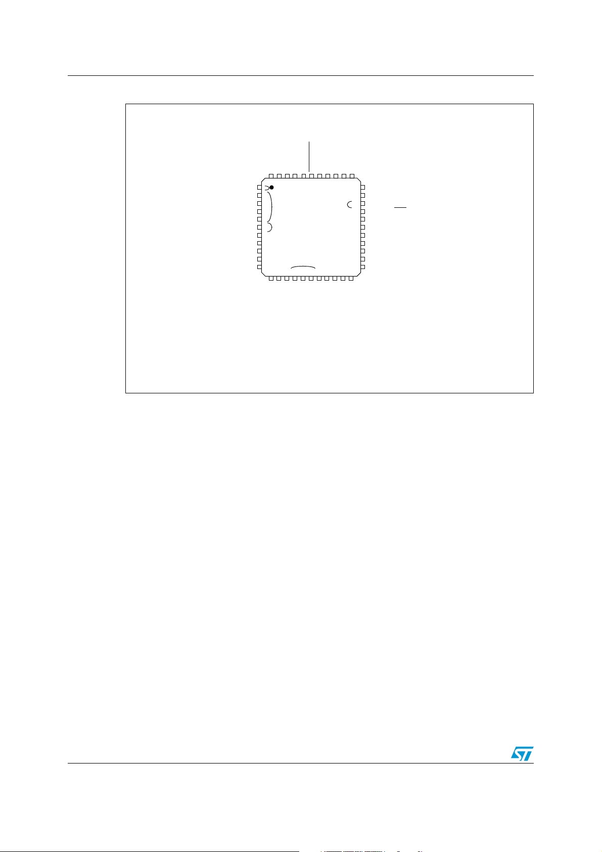
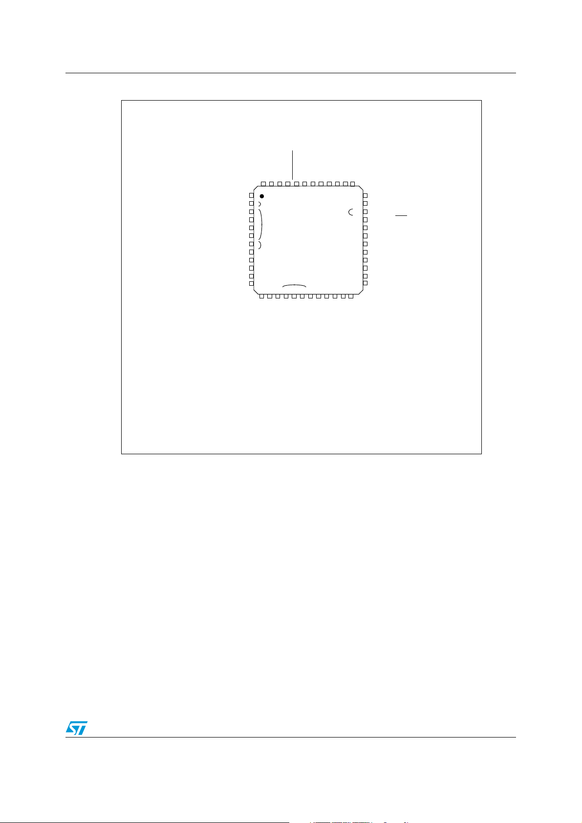
Figure 4. LQFP48 package pinout
Note: For external pin connection guidelines, refer to Section 13: Electrical characteristics.
Doc ID 12321 Rev 6 19/247
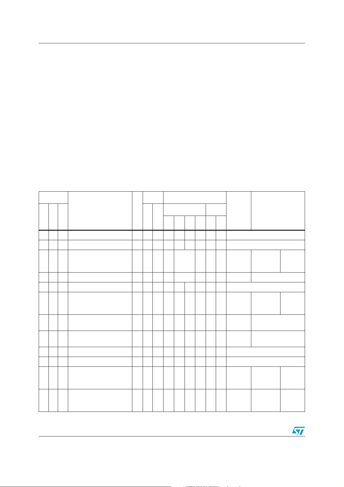
Pin description ST72344xx, ST2345xx
Legend / Abbreviations for Ta b le 3 :
Type: I = input, O = output, S = supply
Input level: A = Dedicated analog input
In/Output level: C
= CMOS 0.3VDD/0.7VDD with input trigger
T
Output level: HS = 20 mA high sink (on N-buffer only)
Port and control configuration:
● Input: float = floating, wpu = weak pull-up, int = interrupt
● Output: OD = open drain
The reset configuration of each pin is shown in bold. This configuration is valid as long as
the device is in reset state.
On the chip, each I/O port may have up to 8 pads. Pads that are not bonded to external pins
are set in input pull-up configuration after reset through the option byte Package selection.
The configuration of these pads must be kept at reset state to avoid added current
consumption.
LQFP44
LQFP48
DDA
SSA
Pin name
(2)
(2)
(3)
S Analog supply voltage
S Analog ground voltage
I/O CTHS X ei1 X X Port F2
Table 3. Device pin description
Pin n°
LQFP32
11314V
21415V
3 15 16 PF0/MCO/AIN8 I/O C
4 16 17 PF1 (HS)/BEEP I/O C
-1718PF2 (HS)
1)
, ana = analog
2)
, PP = push-pull
Level Port
Input
Type
Input
Output
float
(1)
wpu
Output
int
OD
ana
Main
function
(after
reset)
PP
Alternate function
Main clock
T
T
Xei1XXXPort F0
HS X ei1 X X Port F1 Beep signal output
out
(f
OSC
/2)
ADC
analog
input 8
5 18 19 PF4/OCMP1_A/AIN10 I/O C
6 19 20 PF6 (HS)/ICAP1_A I/O C
7 20 21 PF7 (HS)/EXTCLK_A I/O C
-2122V
-2223V
DD_0
SS_0
(2)
(2)
S Digital main supply voltage
S Digital ground voltage
8 23 24 PC0/OCMP2_B/AIN12 I/O C
9 24 27 PC1/OCMP1_B/AIN13 I/O C
T
T
T
T
T
XX XXXPort F4
HS X X X X Port F6
HS X X X X Port F7
XX XXXPort C0
XX XXXPort C1
20/247 Doc ID 12321 Rev 6
Timer A
output
compare 1
ADC
analog
input 10
Timer A Input
Capture 1
Timer A external
clock source
Timer B
output
compare 2
Timer B
output
compare 1
ADC
analog
input 12
ADC
analog
input 13
ST72344xx, ST2345xx Pin description
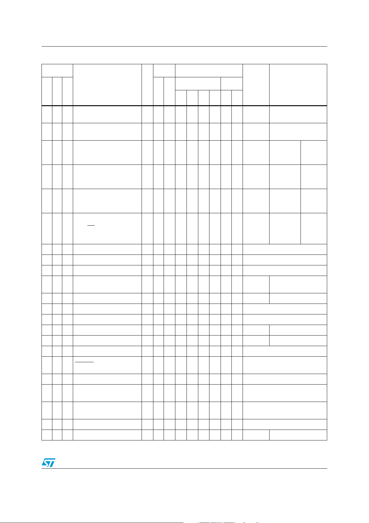
Table 3. Device pin description (continued)
Pin n°
LQFP32
LQFP44
Pin name
LQFP48
Type
10 25 28 PC2 (HS)/ICAP2_B I/O C
11 26 29 PC3 (HS)/ICAP1_B I/O C
12 27 30 PC4/MISO/ICCDATA I/O C
13 28 31 PC5/MOSI/AIN14 I/O C
14 29 32 PC6/SCK/ICCCLK I/O C
15 30 33 PC7/SS
/AIN15 I/O C
16 31 34 PA3 (HS) I/O C
-3235V
-3336V
DD_1
SS_1
- - 37 PD7
(2)
(2)
(3)
/ SCL3SNS I/O CTHS X
S Digital main supply voltage
S Digital ground voltage
Level Port
(1)
Input
Input
Output
HS X X X X Port C2
T
HS X X X X Port C3
T
T
T
T
T
HS X ei0 X X Port A3
T
wpu
float
XX XXPort C4
XX XXXPort C5
XX XXPort C6
XX XXXPort C7
Output
int
ana
(4)
PP
OD
T
Main
function
(after
Alternate function
reset)
Timer B input capture
2
Timer B input capture
1
SPI Master
In / Slave
Out data
SPI Master
Out / Slave
In data
SPI serial
clock
SPI slave
select
(active
low)
ICC data
input
ADC
analog
input 14
ICC
clock
output
ADC
analog
input 15
Port D7 I2C3SNS serial clock
- - 38 PD6
(3)
/ SDA3SNS I/O CTHS X T Port D6 I2C3SNS serial data
17 34 39 PA4 (HS) I/O C
- 35 40 PA5 (HS)
(3)
I/O CTHS X X X X Port A5
18 36 41 PA6 (HS)/SDA I/O C
19 37 42 PA7 (HS)/SCL I/O C
20 38 43 ICCSEL
21 39 44 RESET
22 40 45 V
SS_2
(2)
(5)
I ICC mode selection
I/O C
S Digital ground voltage
23 41 46 OSC2 O
24 42 47 OSC1 I
25 43 48 V
DD_2
(2)
S Digital main supply voltage
26 44 1 PE0/TDO I/O C
HS X X X X Port A4
T
HS X T Port A6 I2C serial data
T
HS X T Port A7 I2C serial clock
T
T
Top priority non maskable
interrupt.
Resonator oscillator inverter
output
External clock input or resonator
oscillator inverter input
T
X X X X Port E0 SCI transmit data out
Doc ID 12321 Rev 6 21/247
Pin description ST72344xx, ST2345xx
Table 3. Device pin description (continued)
Pin n°
Pin name
LQFP32
LQFP44
LQFP48
27 1 2 PE1/RDI I/O C
28 2 3 PB0 I/O C
- 3 4 PB1
- 4 5 PB2
(3)
(3)
29 5 6 PB3 I/O C
30 6 7 PB4 (HS) I/O C
31 7 8 PD0/AIN0 I/O C
32 8 9 PD1/AIN1 I/O C
- 9 10 PD2/AIN2 I/O C
- 10 11 PD3/AIN3 I/O C
- 11 12 PD4/AIN4 I/O C
- 12 13 PD5/AIN5 I/O C
1. In the interrupt input column, “eiX” defines the associated external interrupt vector. If the weak pull-up column (wpu) is
merged with the interrupt column (int), then the I/O configuration is pull-up interrupt input, else the configuration is floating
interrupt input.
2. It is mandatory to connect all available V
3. Pulled-up by hardware when not present on the package.
4. In the open drain output column, “T” defines a true open drain I/O (P-Buffer and protection diode to V
implemented).
5. Internal weak pull-down.
Level Port
Type
Input
Output
T
T
I/O C
T
I/O C
T
T
HS X ei3 X X Port B4
T
T
T
T
T
T
T
DD
and V
pins to the supply voltage and all VSS and V
DDA
Main
Input
float
(1)
wpu
Output
int
ana
OD
function
(after
reset)
PP
Alternate function
X ei0 X X Port E1 SCI receive data in
Xei2 XXPort B0
Xei2 XXPort B1
Xei2 XXPort B2
Xei2XXPort B3
X X X X X Port D0 ADC analog input 0
X X X X X Port D1 ADC analog input 1
X X X X X Port D2 ADC analog input 2
X X X X X Port D3 ADC analog input 3
X X X X X Port D4 ADC analog input 4
X X X X X Port D5 ADC analog input 5
pins to ground.
SSA
are not
DD
22/247 Doc ID 12321 Rev 6
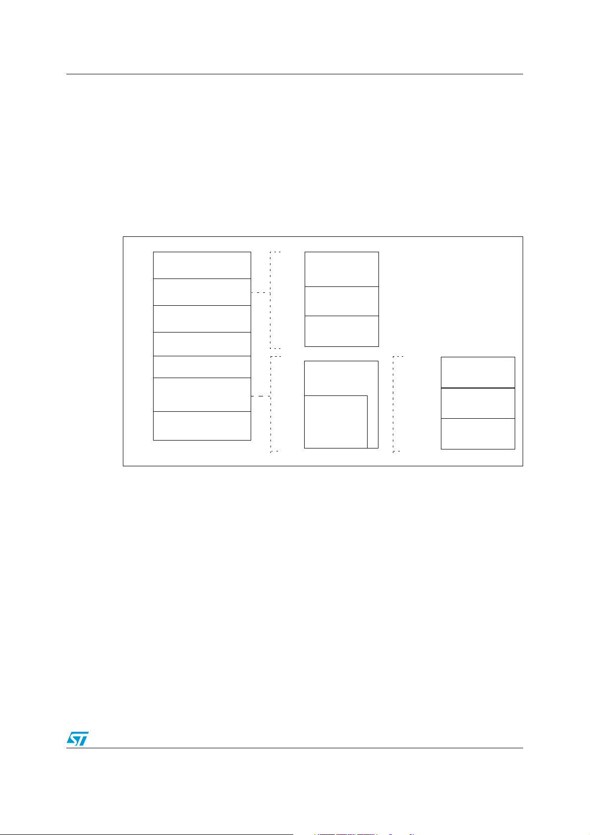
ST72344xx, ST2345xx Register and memory map
0000h
RAM
Program memory
Interrupt & Reset Vectors
HW registers
0080h
007Fh
BFFFh
See Table 4
C000h
FFDFh
FFE0h
FFFFh
Short addressing
RAM (zero page)
256 Bytes stack
16-bit addressing
RAM
0100h
01FFh
047Fh
0080h
0200h
00FFh
(512 or 1K Bytes)
0480h
047Fh
Data EEPROM
(256 Bytes)
Reserved
Reserved
0C00h
0CFFh
0BFFh
0D00h
See Table 17
FFFFh
E000h
C000h
(8 or 16 KBytes)
16 Kbytes
8 Kbytes
SECTOR 2
SECTOR 1
FFFFh
E000h
C000h
SECTOR 0
F000h (4k)
or
FC00h (1k)
or
FE00h (0.5k)
or
FB00h (2k)
3 Register and memory map
As shown in Figure 5, the MCU is capable of addressing 64 Kbytes of memories and I/O
registers.
The available memory locations consist of 128 bytes of register locations, up to 1 Kbyte of
RAM, 256 bytes of Data EEPROM and up to 16 Kbytes of user program memory. The RAM
space includes up to 256 bytes for the stack from 0100h to 01FFh.
The highest address bytes contain the user reset and interrupt vectors.
Figure 5. Memory map
Doc ID 12321 Rev 6 23/247

Register and memory map ST72344xx, ST2345xx
Table 4. Hardware register map
Address Block
0000h
0001h
0002h
0003h
0004h
0005h
0006h
0007h
0008h
0009h
000Ah
000Bh
000Ch
000Dh
000Eh
000Fh
0010h
0011h
Por t A
Por t B
Por t C
Por t D
Por t E
Por t F
(3)
(3)
(3)
(3)
(3)
(3)
Register
label
PA DR
PADDR
PA OR
PBDR
PBDDR
PBOR
PCDR
PCDDR
PCOR
PDADR
PDDDR
PDOR
PEDR
PEDDR
PEOR
PFDR
PFDDR
PFOR
0012h to
0016h
0017h
0018h
RC
RCCRH
RCCRL
Register name
Port A Data Register
Port A Data Direction Register
Port A Option Register
Port B Data Register
Port B Data Direction Register
Port B Option Register
Port C Data Register
Port C Data Direction Register
Port C Option Register
Port D Data Register
Port D Data Direction Register
Port D Option Register
Port E Data Register
Port E Data Direction Register
Port E Option Register
Port F Data Register
Port F Data Direction Register
Port F Option Register
Reserved area (5 bytes)
RC oscillator Control Register High
RC oscillator Control Register Low
Reset status
(1)
(4)
00h
00h
00h
(4)
00h
00h
00h
(4)
00h
00h
00h
(4)
00h
00h
00h
(4)
00h
00h
00h
(4)
00h
00h
00h
FFh
03h
Remarks
(2)
R/W
R/W
R/W
R/W
R/W
R/W
R/W
R/W
R/W
R/W
R/W
R/W
R/W
R/W
R/W
R/W
R/W
R/W
R/W
R/W
0019h Reserved area (1 byte)
001Ah to
001Fh
DM
(5)
Reserved area (6 bytes)
00020h EEPROM EECSR Data EEPROM Control/Status Register 00h R/W
0021h
0022h
0023h
0024h
0025h
0026h
0027h
SPI
ITC
SPIDR
SPICR
SPICSR
ISPR0
ISPR1
ISPR2
ISPR3
SPI Data I/O Register
SPI Control Register
SPI Control Status Register
Interrupt Software Priority Register 0
Interrupt Software Priority Register 1
Interrupt Software Priority Register 2
Interrupt Software Priority Register 3
xxh
0xh
00h
FFh
FFh
FFh
FFh
R/W
R/W
R/W
R/W
R/W
R/W
R/W
0028h EICR External Interrupt Control Register 00h R/W
00029h Flash FCSR Flash Control/Status Register 00h R/W
002Ah WWDG WDGCR Watchdog Control Register 7Fh R/W
002Bh SI SICSR System Integrity Control/Status Register 000x 000xb R/W
002Ch
002Dh
002Eh
002Fh
MCC
AWU
MCCSR
MCCBCR
AWUCSR
AWUPR
Main Clock Control/Status Register
MCC Beep Control Register
AWU Control/Status Register
AWU Prescaler Register
00h
00h
00h
FFh
R/W
R/W
R/W
R/W
0030h WWDG WDGWR Window Watchdog Control Register 7Fh R/W
24/247 Doc ID 12321 Rev 6

ST72344xx, ST2345xx Register and memory map
Table 4. Hardware register map (continued)
Address Block
0031h
0032h
0033h
0034h
0035h
0036h
0037h
0038h
TIMER A
0039h
003Ah
003Bh
003Ch
003Dh
003Eh
003Fh
Register
label
TACR2
TACR1
TA CS R
TA I C1 H R
TAIC1LR
TA OC 1 H R
TA OC 1 L R
TACHR
TA CL R
TAACHR
TA AC L R
TA I C2 H R
TAIC2LR
TA OC 2 H R
TA OC 2 L R
Register name
Timer A Control Register 2
Timer A Control Register 1
Timer A Control/Status Register
Timer A Input Capture 1 High Register
Timer A Input Capture 1 Low Register
Timer A Output Compare 1 High Register
Timer A Output Compare 1 Low Register
Timer A Counter High Register
Timer A Counter Low Register
Timer A Alternate Counter High Register
Timer A Alternate Counter Low Register
Timer A Input Capture 2 High Register
Timer A Input Capture 2 Low Register
Timer A Output Compare 2 High Register
Timer A Output Compare 2 Low Register
0040h Reserved area (1 Byte)
0041h
0042h
0043h
0044h
0045h
0046h
0047h
0048h
0049h
004Ah
004Bh
004Ch
004Dh
004Eh
004Fh
0050h
0051h
0052h
0053h
0054h
0055h
0056h
0057h
0058h
0059h
005Ah
005Bh
005Ch
005Dh
005Eh
TIMER B
SCI
2
I
C
TBCR2
TBCR1
TBCSR
TBIC1HR
TBIC1LR
TBOC1HR
TBOC1LR
TBCHR
TBCLR
TBACHR
TBACLR
TBIC2HR
TBIC2LR
TBOC2HR
TBOC2LR
SCISR
SCIDR
SCIBRR
SCICR1
SCICR2
SCIERPR
SCIETPR
I2CCR
I2CSR1
I2CSR2
I2CCCR
I2COAR1
I2COAR2
I2CDR
Timer B Control Register 2
Timer B Control Register 1
Timer B Control/Status Register
Timer B Input Capture 1 High Register
Timer B Input Capture 1 Low Register
Timer B Output Compare 1 High Register
Timer B Output Compare 1 Low Register
Timer B Counter High Register
Timer B Counter Low Register
Timer B Alternate Counter High Register
Timer B Alternate Counter Low Register
Timer B Input Capture 2 High Register
Timer B Input Capture 2 Low Register
Timer B Output Compare 2 High Register
Timer B Output Compare 2 Low Register
SCI Status Register
SCI Data Register
SCI Baud Rate Register
SCI Control Register 1
SCI Control Register 2
Reserved area
SCI Extended Receive Prescaler Register
SCI Extended Transmit Prescaler Register
2
C Control Register
I
I2C Status Register 1
2
C Status Register 2
I
I2C Clock Control Register
I2C Own Address Register 1
2
C Own Address Register2
I
I2C Data Register
005Fh Reserved area (1 byte)
Reset status
(1)
00h
00h
xxh
xxh
xxh
80h
00h
FFh
FCh
FFh
FCh
xxh
xxh
80h
00h
00h
00h
xxh
xxh
xxh
80h
00h
FFh
FCh
FFh
FCh
xxh
xxh
80h
00h
C0h
xxh
00h
x000 0000b
00h
-00h
00h
00h
00h
00h
00h
00h
40h
00h
Remarks
(2)
R/W
R/W
R/W
Read Only
Read Only
R/W
R/W
Read Only
Read Only
Read Only
Read Only
Read Only
Read Only
R/W
R/W
R/W
R/W
R/W
Read Only
Read Only
R/W
R/W
Read Only
Read Only
Read Only
Read Only
Read Only
Read Only
R/W
R/W
Read Only
R/W
R/W
R/W
R/W
R/W
R/W
R/W
Read Only
Read Only
R/W
R/W
R/W
R/W
Doc ID 12321 Rev 6 25/247

Register and memory map ST72344xx, ST2345xx
Table 4. Hardware register map (continued)
Address Block
0060h
0061h
0062h
0063h
0064h
0065h
2
C3SNS
I
0066h
0067h
0068h
0069h
0070h
0071h
ADC
0072h
0073h to
007Fh
1. x = undefined.
2. R/W = read/write.
3. The bits associated with unavailable pins must always keep their reset value.
4. The contents of the I/O port DR registers are readable only in output configuration. In input configuration, the values of the
I/O pins are returned instead of the DR register contents.
5. For a description of the Debug Module registers, see ST7 ICC protocol reference manual.
Register
label
I2C3SCR1
I2C3SCR2
I2C3SSR
I2C3SBCR
I2C3SSAR1
I2C3SCAR1
I2C3SSAR2
I2C3SCAR2
I2C3SSAR3
I2C3SCAR3
ADCCSR
ADCDRH
ADCDRL
Register name
2
C3SNS Control Register 1
I
I2C3SNS Control Register 2
I2C3SNS Status Register
2
C3SNS Byte Count Register
I
I2C3SNS Slave Address 1 Register
I2C3SNS Current Address 1 Register
2
C3SNS Slave Address 2 Register
I
I2C3SNS Current Address 2 Register
I2C3SNS Slave Address 3 Register
2
C3SNS Current Address 3 Register
I
A/D Control Status Register
A/D Data Register High
A/D Data Low Register
Reserved area (13 bytes)
Reset status
(1)
00h
00h
00h
00h
00h
00h
00h
00h
00h
00h
00h
xxh
0000 00xxb
Remarks
(2)
R/W
R/W
Read Only
Read Only
R/W
R/W
R/W
R/W
R/W
R/W
R/W
Read Only
Read Only
26/247 Doc ID 12321 Rev 6

ST72344xx, ST2345xx Flash program memory
4 Flash program memory
4.1 Introduction
The ST7 single voltage extended Flash (XFlash) is a non-volatile memory that can be
electrically erased and programmed either on a byte-by-byte basis or up to 32 bytes in
parallel.
The XFlash devices can be programmed off-board (plugged in a programming tool) or onboard using In-Circuit Programming or In-Application Programming.
The array matrix organization allows each sector to be erased and reprogrammed without
affecting other sectors.
4.2 Main features
● ICP (in-circuit programming)
● IAP (in-application programming)
● ICT (in-circuit testing) for downloading and executing user application test patterns in
RAM
● Sector 0 size configurable by option byte
● Read-out and write protection
4.3 Programming modes
The ST7 can be programmed in three different ways:
● Insertion in a programming tool
In this mode, Flash sectors 0 and 1, option byte row and data EEPROM (if present) can
be programmed or erased.
● In-circuit programming
In this mode, Flash sectors 0 and 1, option byte row and data EEPROM (if present) can
be programmed or erased without removing the device from the application board.
● In-application programming
In this mode, sector 1 and data EEPROM (if present) can be programmed or erased
without removing the device from the application board and while the application is
running.
Doc ID 12321 Rev 6 27/247

Flash program memory ST72344xx, ST2345xx
4.3.1 In-circuit programming (ICP)
ICP uses a protocol called ICC (in-circuit communication) which allows an ST7 plugged on a
printed circuit board (PCB) to communicate with an external programming device connected
via cable. ICP is performed in three steps:
Switch the ST7 to ICC mode (in-circuit communications). This is done by driving a specific
signal sequence on the ICCCLK/DATA pins while the RESET
pin is pulled low. When the
ST7 enters ICC mode, it fetches a specific reset vector which points to the ST7 System
Memory containing the ICC protocol routine. This routine enables the ST7 to receive bytes
from the ICC interface.
● Download ICP Driver code in RAM from the ICCDATA pin
● Execute ICP Driver code in RAM to program the Flash memory
Depending on the ICP Driver code downloaded in RAM, Flash memory programming can
be fully customized (number of bytes to program, program locations, or selection of the
serial communication interface for downloading).
4.3.2 In-application programming (IAP)
This mode uses an IAP Driver program previously programmed in Sector 0 by the user (in
ICP mode).
This mode is fully controlled by user software. This allows it to be adapted to the user
application (user-defined strategy for entering programming mode, choice of
communications protocol used to fetch the data to be stored etc.)
IAP mode can be used to program any memory areas except Sector 0, which is write/erase
protected to allow recovery in case errors occur during the programming operation.
4.4 ICC interface
ICP needs a minimum of 4 and up to 7 pins to be connected to the programming tool. These
pins are:
● RESET: device reset
● V
● ICCCLK: ICC output serial clock pin
● ICCDATA: ICC input serial data pin
● ICCSEL: ICC selection
● OSC1: main clock input for external source (not required on devices without
● V
Note: 1 If the ICCCLK or ICCDATA pins are only used as outputs in the application, no signal
isolation is necessary. As soon as the Programming Tool is plugged to the board, even if an
ICC session is not in progress, the ICCCLK and ICCDATA pins are not available for the
application. If they are used as inputs by the application, isolation such as a serial resistor
has to be implemented in case another device forces the signal. Refer to the Programming
Tool documentation for recommended resistor values.
2 During the ICP session, the programming tool must control the RESET
conflicts between the programming tool and the application reset circuit if it drives more than
5 mA at high level (push pull output or pull-up resistor<1,000). A schottky diode can be used
: device power supply ground
SS
OSC1/OSC2 pins)
: application board power supply (optional, see Note 3)
DD
pin. This can lead to
28/247 Doc ID 12321 Rev 6
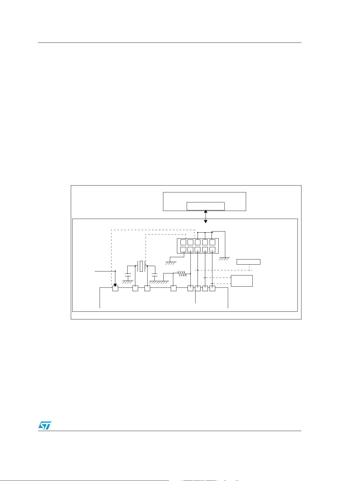
ST72344xx, ST2345xx Flash program memory
ICC CONNECTOR
ICCDATA
ICCCLK
RESET
VDD
HE10 CONNECTOR TYPE
APPLICATION
POWER SUPPLY
1
246810
975 3
PROGRAMMING TOOL
ICC CONNECTOR
APPLICATION BOARD
ICC Cable
(See Note 3)
10kΩ
VSS
ICCSEL
ST7
C
L2
C
L1
OSC1
OSC2
OPTIONAL
See Note 1
See Note 2
APPLICATION
RESET SOURCE
APPLICATION
I/O
(See Note 4)
to isolate the application reset circuit in this case. When using a classical RC network with
R>1,000 or a reset management IC with open drain output and pull-up resistor>1,000, no
additional components are needed. In all cases the user must ensure that no external reset
is generated by the application during the ICC session.
3 The use of Pin 7 of the ICC connector depends on the Programming Tool architecture. This
pin must be connected when using most ST Programming Tools (it is used to monitor the
application power supply). Please refer to the Programming Tool manual.
4 Pin 9 has to be connected to the OSC1 pin of the ST7 when the clock is not available in the
application or if the selected clock option is not programmed in the option byte. ST7 devices
with multi-oscillator capability need to have OSC2 grounded in this case.
5 In “enabled option byte” mode (38-pulse ICC mode), the internal RC oscillator is forced as a
clock source, regardless of the selection in the option byte.
Caution: During normal operation, the ICCCLK pin must be internally or externally pulled- up
(external pull-up of 10 kΩ mandatory in noisy environment) to avoid entering ICC mode
unexpectedly during a reset. In the application, even if the pin is configured as an output,
any reset will put it back in input pull-up.
Figure 6. Typical ICC interface
4.5 Memory protection
There are two different types of memory protection: Read Out Protection and Write/Erase
Protection which can be applied individually.
4.5.1 Readout protection
Readout protection, when selected, provides a protection against program memory content
extraction and against write access to Flash memory. Even if no protection can be
considered as totally unbreakable, the feature provides a very high level of protection for a
general purpose microcontroller. Both program and data E
Doc ID 12321 Rev 6 29/247
2
memory are protected.

Flash program memory ST72344xx, ST2345xx
In Flash devices, this protection is removed by reprogramming the option. In this case, both
program and data E
2
memory are automatically erased, and the device can be
reprogrammed.
Read-out protection selection depends on the device type:
● In Flash devices, it is enabled and removed through the FMP_R bit in the option byte.
● In ROM devices, it is enabled by mask option specified in the Option List.
4.5.2 Flash write/erase protection
Write/erase protection, when set, makes it impossible to both overwrite and erase program
memory. It does not apply to E
applications and prevent any change being made to the memory content.
Warning: Once set, Write/erase protection can never be removed. A
write-protected Flash device is no longer reprogrammable.
Write/erase protection is enabled through the FMP_W bit in the option byte.
2
data. Its purpose is to provide advanced security to
4.6 Register description
4.6.1 Flash control/status register (FCSR)
Reset value: 0000 0000 (00h)
1st RASS Key: 0101 0110 (56h)
2nd RASS Key: 1010 1110 (AEh)
7 0
00000OPTLATPGM
Read/Write
Note: This register is reserved for programming using ICP, IAP or other programming methods. It
controls the XFlash programming and erasing operations. For details on XFlash
programming, refer to the ST7 Flash Programming Reference Manual.
When an EPB or another programming tool is used (in socket or ICP mode), the RASS keys
are sent automatically.
30/247 Doc ID 12321 Rev 6

ST72344xx, ST2345xx Data EEPROM
EECSR
HIGH VOLTAGE
PUMP
0 E2LAT00 0 0 0 E2PGM
EEPROM
MEMORY MATRIX
(1 ROW = 32 x 8 BITS)
ADDRESS
DECODER
DATA
MULTIPLEXER
32 x 8 BITS
DATA LATCHES
ROW
DECODER
DATA BUS
4
4
4
128128
ADDRESS BUS
5 Data EEPROM
5.1 Introduction
The electrically erasable programmable read only memory can be used as a non-volatile
backup for storing data. Using the EEPROM requires a basic access protocol described in
this chapter.
5.2 Main features
● Up to 32 bytes programmed in the same cycle
● EEPROM mono-voltage (charge pump)
● Chained erase and programming cycles
● Internal control of the global programming cycle duration
● Wait mode management
● Readout protection
Figure 7. EEPROM block diagram
5.3 Memory access
The Data EEPROM memory read/write access modes are controlled by the E2LAT bit of the
EEPROM Control/Status register (EECSR). The flowchart in Figure 8 describes these
different memory access modes.
Doc ID 12321 Rev 6 31/247

Data EEPROM ST72344xx, ST2345xx
READ MODE
E2LAT = 0
E2PGM = 0
WRITE MODE
E2LAT = 1
E2PGM = 0
READ BYTES
IN EEPROM AREA
WRITE UP TO 32 BYTES
IN EEPROM AREA
(with the same 11 MSB of the address)
START PROGRAMMING CYCLE
E2LAT=1
E2PGM=1 (set by software)
E2PGM
01
CLEARED BY HARDWARE
Read operation (E2LAT = 0)
The EEPROM can be read as a normal ROM location when the E2LAT bit of the EECSR
register is cleared.
On this device, Data EEPROM can also be used to execute machine code. Take care not to
write to the Data EEPROM while executing from it. This would result in an unexpected code
being executed.
Write operation (E2LAT = 1)
To access the write mode, the E2LAT bit has to be set by software (the E2PGM bit remains
cleared). When a write access to the EEPROM area occurs, the value is latched inside the
32 data latches according to its address.
When E2PGM bit is set by the software, all the previous bytes written in the data latches (up
to 32) are programmed in the EEPROM cells. The effective high address (row) is
determined by the last EEPROM write sequence. To avoid wrong programming, the user
must take care that all the bytes written between two programming sequences have the
same high address: only the five Least Significant Bits of the address can change.
The programming cycle is fully completed when the E2PGM bit is cleared.
Note: Care should be taken during the programming cycle. Writing to the same memory location
will over-program the memory (logical AND between the two write access data results)
because the data latches are only cleared at the end of the programming cycle and by the
falling edge of the E2LAT bit.
It is not possible to read the latched data.
This note is illustrated by the Figure 10.
Figure 8. Data EEPROM programming flowchart
32/247 Doc ID 12321 Rev 6

ST72344xx, ST2345xx Data EEPROM
Byte 1 Byte 2 Byte 32
PHASE 1
Programming cycle
Read operation impossible
PHASE 2
Read operation possible
E2LAT bit
E2PGM bit
Writing data latches
Waiting E2PGM and E2LAT to fall
Set by USER application
Cleared by hardware
⇓ Row / Byte ⇒ 0 1 2 3 ... 30 31 Physical address
0 00h...1Fh
1 20h...3Fh
...
N Nx20h...Nx20h+1Fh
Row
definition
Figure 9. Data EEPROM write operation
Note: If a programming cycle is interrupted (by reset action), the integrity of the data in memory
will not be guaranteed.
5.4 Power saving modes
5.4.1 Wait mode
The data EEPROM can enter Wait mode on execution of the WFI instruction of the
microcontroller or when the microcontroller enters Active Halt mode.The data EEPROM will
immediately enter this mode if there is no programming in progress, otherwise the data
EEPROM will finish the cycle and then enter Wait mode.
5.4.2 Active-halt mode
Refer to Wait mode.
5.4.3 Halt mode
The data EEPROM immediately enters Halt mode if the microcontroller executes the Halt
instruction. Therefore the EEPROM will stop the function in progress, and data may be
corrupted.
5.5 Access error handling
If a read access occurs while E2LAT = 1, then the data bus will not be driven.
If a write access occurs while E2LAT = 0, then the data on the bus will not be latched.
If a programming cycle is interrupted (by reset action), the integrity of the data in memory
will not be guaranteed.
Doc ID 12321 Rev 6 33/247

Data EEPROM ST72344xx, ST2345xx
E2LAT
ERASE CYCLE WRITE CYCLE
E2PGM
t
PROG
READ OPERATION NOT POSSIBLE
WRITE OF
DATA
READ OPERATION POSSIBLE
INTERNAL
PROGRAMMING
VOLTAGE
LATCHES
I bit in CC register
All interrupts must be masked
1)
Note 1: refer to Programming of EEPROM data
5.6 Data EEPROM readout protection
The readout protection is enabled through an option bit (see Section 15.1: Option bytes).
When this option is selected, the programs and data stored in the EEPROM memory are
protected against read-out (including a rewrite protection). In Flash devices, when this
protection is removed by reprogramming the option byte, the entire Program memory and
EEPROM is first automatically erased.
Note: Both program memory and data EEPROM are protected using the same option bit.
Figure 10. Data EEPROM programming cycle
34/247 Doc ID 12321 Rev 6

ST72344xx, ST2345xx Data EEPROM
5.7 Register description
5.7.1 EEPROM control/status register (EECSR)
Reset value: 0000 0000 (00h)
7 0
000000E2LATE2PGM
Read/Write
Bits 7:2 = Reserved, forced by hardware to 0.
Bit 1 = E2LAT Latch Access Transfer
This bit is set by software. It is cleared by hardware at the end of the programming
cycle. It can only be cleared by software if the E2PGM bit is cleared.
0: Read mode
1: Write mode
Bit 0 = E2PGM Programming control and status
This bit is set by software to begin the programming cycle. At the end of the
programming cycle, this bit is cleared by hardware.
0: Programming finished or not yet started
1: Programming cycle is in progress
Note: If the E2PGM bit is cleared during the programming cycle, the memory data is not
guaranteed.
Table 5. Data EEPROM register map and reset values
Address
(Hex.)
0020h
Register
label
EECSR
Reset value000000
76543210
E2LAT0E2PGM
0
Doc ID 12321 Rev 6 35/247

Central processing unit ST72344xx, ST2345xx
6 Central processing unit
6.1 Introduction
This CPU has a full 8-bit architecture and contains six internal registers allowing efficient 8bit data manipulation.
6.2 Main features
● Enable executing 63 basic instructions
● Fast 8-bit by 8-bit multiply
● 17 main addressing modes (with indirect addressing mode)
● Two 8-bit index registers
● 16-bit stack pointer
● Low power Halt and Wait modes
● Priority maskable hardware interrupts
● Non-maskable software/hardware interrupts
6.3 CPU registers
The six CPU registers shown in Figure 11 are not present in the memory mapping and are
accessed by specific instructions.
Accumulator (A)
The Accumulator is an 8-bit general purpose register used to hold operands and the results
of the arithmetic and logic calculations and to manipulate data.
Index Registers (X and Y)
These 8-bit registers are used to create effective addresses or as temporary storage areas
for data manipulation. (The Cross-Assembler generates a precede instruction (PRE) to
indicate that the following instruction refers to the Y register.)
The Y register is not affected by the interrupt automatic procedures.
Program Counter (PC)
The program counter is a 16-bit register containing the address of the next instruction to be
executed by the CPU. It is made of two 8-bit registers PCL (Program Counter Low which is
the LSB) and PCH (Program Counter High which is the MSB).
36/247 Doc ID 12321 Rev 6

ST72344xx, ST2345xx Central processing unit
ACCUMULATOR
X INDEX REGISTER
Y INDEX REGISTER
STACK POINTER
CONDITION CODE REGISTER
PROGRAM COUNTER
70
1C1I1HI0NZ
RESET VALUE = RESET VECTOR @ FFFEh-FFFFh
70
70
70
0
7
15 8
PCH
PCL
15
8
70
RESET VALUE = STACK HIGHER ADDRESS
RESET VALUE =
1X11X1XX
RESET VALUE = XXh
RESET VALUE = XXh
RESET VALUE = XXh
X = Undefined Value
Figure 11. CPU registers
6.3.1 Condition code register (CC)
Reset value: 111x1xxx
7 0
11I1HI0NZC
The 8-bit Condition Code register contains the interrupt masks and four flags representative
of the result of the instruction just executed. This register can also be handled by the PUSH
and POP instructions.
These bits can be individually tested and/or controlled by specific instructions.
Arithmetic management bits
Bit 4 = H Half carry.
This bit is set by hardware when a carry occurs between bits 3 and 4 of the ALU during
an ADD or ADC instructions. It is reset by hardware during the same instructions.
0: No half carry has occurred.
1: A half carry has occurred.
This bit is tested using the JRH or JRNH instruction. The H bit is useful in BCD
arithmetic subroutines.
Read/Write
Doc ID 12321 Rev 6 37/247

Central processing unit ST72344xx, ST2345xx
Bit 2 = N Negative.
This bit is set and cleared by hardware. It is representative of the result sign of the last
arithmetic, logical or data manipulation. It’s a copy of the result 7
th
bit.
0: The result of the last operation is positive or null.
1: The result of the last operation is negative
(that is, the most significant bit is a logic 1).
This bit is accessed by the JRMI and JRPL instructions.
Bit 1 = Z Zero.
This bit is set and cleared by hardware. This bit indicates that the result of the last
arithmetic, logical or data manipulation is zero.
0: The result of the last operation is different from zero.
1: The result of the last operation is zero.
This bit is accessed by the JREQ and JRNE test instructions.
Bit 0 = C Carry/borrow.
This bit is set and cleared by hardware and software. It indicates an overflow or an
underflow has occurred during the last arithmetic operation.
0: No overflow or underflow has occurred.
1: An overflow or underflow has occurred.
This bit is driven by the SCF and RCF instructions and tested by the JRC and JRNC
instructions. It is also affected by the “bit test and branch”, shift and rotate instructions.
Interrupt management bits
Bits 5,3 = I1, I0 Interrupt
The combination of the I1 and I0 bits gives the current interrupt software priority.
Table 6. Interrupt software priority
Priority I1 I0
Level 0 (main) 1 0
Level 1 0 1
Level 2 0 0
Level 3 (= interrupt disable) 1 1
These two bits are set/cleared by hardware when entering in interrupt. The loaded value is
given by the corresponding bits in the interrupt software priority registers (IxSPR). They can
be also set/cleared by software with the RIM, SIM, IRET, HALT, WFI and PUSH/POP
instructions.
See the interrupt management chapter for more details.
38/247 Doc ID 12321 Rev 6

ST72344xx, ST2345xx Central processing unit
6.3.2 Stack pointer (SP)
Reset value: 01 FFh
15 8
00000001
Read/Write
7 0
SP7 SP6 SP5 SP4 SP3 SP2 SP1 SP0
Read/Write
The Stack pointer is a 16-bit register which is always pointing to the next free location in the
stack. It is then decremented after data has been pushed onto the stack and incremented
before data is popped from the stack (see Figure 12).
Since the stack is 256 bytes deep, the 8 most significant bits are forced by hardware.
Following an MCU Reset, or after a Reset Stack Pointer instruction (RSP), the Stack pointer
contains its reset value (the SP7 to SP0 bits are set) which is the stack higher address.
The least significant byte of the Stack pointer (called S) can be directly accessed by an LD
instruction.
Note: When the lower limit is exceeded, the Stack pointer wraps around to the stack upper limit,
without indicating the stack overflow. The previously stored information is then overwritten
and therefore lost. The stack also wraps in case of an underflow.
The stack is used to save the return address during a subroutine call and the CPU context
during an interrupt. The user may also directly manipulate the stack by means of the PUSH
and POP instructions. In the case of an interrupt, the PCL is stored at the first location
pointed to by the SP. Then the other registers are stored in the next locations as shown in
Figure 12.
● When an interrupt is received, the SP is decremented and the context is pushed on the
stack.
● On return from interrupt, the SP is incremented and the context is popped from the
stack.
A subroutine call occupies two locations and an interrupt five locations in the stack area.
Doc ID 12321 Rev 6 39/247

Central processing unit ST72344xx, ST2345xx
PCH
PCL
SP
PCH
PCL
SP
PCL
PCH
X
A
CC
PCH
PCL
SP
PCL
PCH
X
A
CC
PCH
PCL
SP
PCL
PCH
X
A
CC
PCH
PCL
SP
SP
Y
CALL
Subroutine
Interrupt
Event
PUSH Y POP Y IRET
RET
or RSP
@ 01FFh
@ 0100h
Stack Higher Address = 01FFh
Stack Lower Address =
0100h
Figure 12. Stack manipulation example
40/247 Doc ID 12321 Rev 6

ST72344xx, ST2345xx Supply, reset and clock management
CR9 CR8 CR7 CR6 CR5 CR4 CR3 CR2 CR1 CR0
RCCRH/RCCRL Register
Tunable
RC Oscillator
/2
DIVIDER
OSC
1-16 MHz
OSC Option bit
/2
DIVIDER
PLL 1 MHz --> 8 MHz
PLL 1 MHz --> 4 MHz
External Clock (0.5-8 MHz)
RC Clock (1 MHz)
PLL Clock 8/4 MHz
OSC, PLLOFF
OSCRANGE[2:0]
Option bits
Crystal OSC (0.5-8 MHz)
PLLx4x8
OSC1
OSC2
f
OSC2
MAIN CLOCK
CONTROLLER
WITH REAL-TIME
CLOCK(MCC/RTC)
f
CPU
8 MHz
4 MHz
1 MHz
Option bit
/2
DIVIDER*
DIV2EN
Option bit*
*not available if PLLx4 is enabled
7 Supply, reset and clock management
The device includes a range of utility features for securing the application in critical
situations (for example in case of a power brown-out), and reducing the number of external
components.
7.1 Main features
● Clock management
– 1 MHz high-accuracy internal RC oscillator (enabled by option byte)
– 1 to 16 MHz External crystal/ceramic resonator (enabled by option byte)
– External Clock Input (enabled by option byte)
– PLL for multiplying the frequency by 8 or 4 (enabled by option byte)
● Reset sequence manager (RSM)
● System integrity management (SI)
– Main supply low voltage detection (LVD) with reset generation (enabled by option
byte)
– Auxiliary voltage detector (AVD) with interrupt capability for monitoring the main
supply (enabled by option byte)
Figure 13. Clock, reset and supply block diagram
Doc ID 12321 Rev 6 41/247

Supply, reset and clock management ST72344xx, ST2345xx
4/8 x
freq.
LOCKED bit set
t
STAB
t
LOCK
input
Output freq.
t
STARTUP
t
7.2 Phase locked loop
The PLL can be used to multiply a 1 MHz frequency from the RC oscillator or the external
clock by 4 or 8 to obtain f
of 4 or 8 is selected by 3 option bits. Refer to Ta bl e 7 for the PLL configuration depending on
the required frequency and the application voltage. Refer to Section 15.1 for the option byte
description.
Table 7. PLL configurations
of 4 or 8 MHz. The PLL is enabled and the multiplication factor
OSC
Targ et ra ti o V
(1)
x4
x4
x8 x8 OFF
1. For a target ratio of x4 between 3.3 V - 3.65 V, this is the recommended configuration.
DD
2.7 V - 3.65 V x4 OFF
3.3 V - 5.5 V
PLL ratio DIV2
x8 ON
Figure 14. PLL output frequency timing diagram
When the PLL is started, after reset or wakeup from Halt mode or AWUFH mode, it outputs
the clock after a delay of t
STARTUP
.
When the PLL output signal reaches the operating frequency, the LOCKED bit in the
SICSCR register is set. Full PLL accuracy (ACC
t
(see Figure 14).
STAB
) is reached after a stabilization time of
PLL
Refer to Section 7.6.5: Register description for a description of the LOCKED bit in the
SICSR register.
Caution: The PLL is not recommended for applications where timing accuracy is required.
Caution: When the RC oscillator and the PLL are enabled, it is recommended to calibrate this clock
through the RCCRH and RCCRL registers.
42/247 Doc ID 12321 Rev 6

ST72344xx, ST2345xx Supply, reset and clock management
7.3 Multioscillator (MO)
The main clock of the ST7 can be generated by three different source types coming from the
multioscillator block:
● an external source
● 4 crystal or ceramic resonator oscillators
● an internal high-accuracy RC oscillator
Each oscillator is optimized for a given frequency range in terms of consumption and is
selectable through the option byte. The associated hardware configurations are shown in
Ta bl e 8 . Refer to Section 13: Electrical characteristics for more details.
Caution: The OSC1 and/or OSC2 pins must not be left unconnected. For the purposes of Failure
Mode and Effect Analysis, it should be noted that if the OSC1 and/or OSC2 pins are left
unconnected, the ST7 main oscillator may start and, in this configuration, could generate an
f
clock frequency in excess of the allowed maximum (>16 MHz), putting the ST7 in an
OSC
unsafe/undefined state. The product behavior must therefore be considered undefined when
the OSC pins are left unconnected.
7.3.1 External clock source
In this external clock mode, a clock signal (square, sinus or triangle) with ~50% duty cycle
has to drive the OSC1 pin while the OSC2 pin is tied to ground.
7.3.2 Crystal/ceramic oscillators
This family of oscillators has the advantage of producing a very accurate rate on the main
clock of the ST7. The selection within a list of 4 oscillators with different frequency ranges
has to be done by option byte in order to reduce consumption (refer to Section 15.1: Option
bytes for more details on the frequency ranges). In this mode of the multi-oscillator, the
resonator and the load capacitors have to be placed as close as possible to the oscillator
pins in order to minimize output distortion and startup stabilization time. The loading
capacitance values must be adjusted according to the selected oscillator.
These oscillators are not stopped during the reset phase to avoid losing time in the oscillator
startup phase.
Doc ID 12321 Rev 6 43/247

Supply, reset and clock management ST72344xx, ST2345xx
OSC1 OSC2
EXTERNAL
ST7
SOURCE
OSC1 OSC2
LOAD
CAPACITORS
ST7
C
L2
C
L1
OSC1 OSC2
ST7
Table 8. ST7 clock sources
Hardware configuration
External clockCrystal/ceramic resonatorsInternal RC oscillator
44/247 Doc ID 12321 Rev 6

ST72344xx, ST2345xx Supply, reset and clock management
7.3.3 Internal RC oscillator
The device contains a high-precision internal RC oscillator. It must be calibrated to obtain
the frequency required in the application. This is done by software writing a calibration value
in the RCCRH and RCCRL Registers.
Whenever the microcontroller is reset, the RCCR returns to its default value (FF 03h), i.e.
each time the device is reset, the calibration value must be loaded in the RCCRH and
RCCRL registers. Predefined calibration values are stored in XFlash for 3 and 5V V
supply voltages at 25 °C, as shown in the following table:
Table 9. Calibration values
RCCR Conditions Address
V
= 5 V
f
f
T
RC
V
T
RC
A
A
DD
= 25 °C
= 1 MHz
= 3 V
DD
= 25 °C
= 1 MHz
BEE0, BEE1
BEE4, BEE5
RCCR0
RCCR1
Note: To improve clock stability, it is recommended to place a decoupling capacitor between the
V
and VSS pins.
DD
These two 10-bit values are systematically programmed by ST.
RCCR0 and RCCR1 calibration values will be erased if the read-out protection bit is reset
after it has been set. See Section 4.5: Memory protection.
DD
Caution: If the voltage or temperature conditions change in the application, the frequency may need
to be recalibrated.
Refer to application note AN1324 for information on how to calibrate the RC frequency using
an external reference signal.
7.4 Register description
7.4.1 RC control register (RCCRH)
Reset value: 1111 1111 (FFh)
7 0
CR9 CR8 CR7 CR6 CR5 CR4 CR3 CR2
Read/Write
Bits 7:0 = CR[9:2] RC oscillator frequency adjustment bits
Doc ID 12321 Rev 6 45/247

Supply, reset and clock management ST72344xx, ST2345xx
7.4.2 RC control register (RCCRL)
Reset value: 0000 0011 (03h)
7 0
000000CR1CR0
Read/Write
Bits 7:2 = Reserved, must be kept cleared.
Bits 1:0 = CR[1:0] RC Oscillator Frequency Adjustment Bits
This 10-bit value must be written immediately after reset to adjust the RC oscillator
frequency in order to obtain the specified accuracy. The application can store the
correct value for each voltage range in EEPROM and write it to this register at startup.
0000h = maximum available frequency
03FFh = lowest available frequency
Note: To tune the oscillator, write a series of different values in the register until the correct
frequency is reached. The fastest method is to use a dichotomy starting with 200h.
7.5 Reset sequence manager (RSM)
7.5.1 Introduction
The reset sequence manager includes three reset sources as shown in Figure 16:
● External RESET source pulse
● Internal LVD reset (low voltage detection)
● Internal watchdog reset
Note: A reset can also be triggered following the detection of an illegal opcode or prebyte code.
Refer to Section 12.2.1: Illegal opcode reset on page 196 for further details.
These sources act on the RESET
The reset service routine vector is fixed at addresses FFFEh-FFFFh in the ST7 memory
map.
The basic reset sequence consists of 3 phases as shown in Figure 15:
● Active phase depending on the reset source
● 256 or 4096 CPU clock cycle delay (selected by option byte)
● reset vector fetch
Caution: When the ST7 is unprogrammed or fully erased, the Flash is blank and the reset vector is
not programmed. For this reason, it is recommended to keep the RESET
until programming mode is entered, in order to avoid unwanted behavior.
The 256 or 4096 CPU clock cycle delay allows the oscillator to stabilize and ensures that
recovery has taken place from the Reset state. The shorter or longer clock cycle delay
should be selected by option byte to correspond to the stabilization time of the external
oscillator used in the application (see Section 15.1: Option bytes).
pin and it is always kept low during the delay phase.
pin in low state
The reset vector fetch phase duration is 2 clock cycles.
46/247 Doc ID 12321 Rev 6

ST72344xx, ST2345xx Supply, reset and clock management
RESET
Active phase
Internal Reset
256 or 4096 clock cycles
Fetch
vector
RESET
R
ON
V
DD
WATCHDOG RESET
LVD RESET
INTERNAL
RESET
PULSE
GENERATOR
Filter
ILLEGAL OPCODE RESET
(1)
Figure 15. reset sequence phases
7.5.2 Asynchronous external RESET pin
The RESET pin is both an input and an open-drain output with integrated RON weak pull-up
resistor. This pull-up has no fixed value but varies in accordance with the input voltage. It
can be pulled low by external circuitry to reset the device. See Section 13: Electrical
characteristics for more details.
A reset signal originating from an external source must have a duration of at least t
h(RSTL)in
in order to be recognized (see Figure 17). This detection is asynchronous and therefore the
MCU can enter reset state even in Halt mode.
Figure 16. Reset block diagram
1. See Section 12.2.1: Illegal opcode reset for more details on illegal opcode reset conditions.
The RESET pin is an asynchronous signal which plays a major role in EMS performance. In
a noisy environment, it is recommended to follow the guidelines mentioned in Section 13:
Electrical characteristics.
If the external RESET
the signal on the RESET
pulse is shorter than t
pin may be stretched. Otherwise the delay will not be applied (see
long ext. Reset in Figure 17). Starting from the external RESET
device RESET
pin acts as an output that is pulled low during at least t
7.5.3 External power-on reset
If the LVD is disabled by option byte, to start up the microcontroller correctly, the user must
ensure by means of an external reset circuit that the reset signal is held low until V
the minimum level specified for the selected f
conditions).
A proper reset signal for a slow rising V
RC network connected to the RESET
w(RSTL)out
(see short ext. Reset in Figure 17),
pulse recognition, the
w(RSTL)out
frequency (see Section 13.3: Operating
OSC
supply can generally be provided by an external
DD
.
is over
DD
pin.
Doc ID 12321 Rev 6 47/247

Supply, reset and clock management ST72344xx, ST2345xx
V
DD
Run
RESET PIN
EXTERNAL
WATCHDOG
ACTIVE PHASE
V
IT+(LVD)
V
IT-(LVD)
t
h(RSTL)in
t
w(RSTL)out
Run
t
h(RSTL)in
ACTIVE
WATCHDOG UNDERFLOW
t
w(RSTL)out
Run Run Run
RESET
RESET
SOURCE
SHORT EXT.
RESET
LVD
RESET
LONG EXT.
RESET
WATCHDOG
RESET
INTERNAL RESET (256 or 4096 T
CPU
)
VECTOR FETCH
t
w(RSTL)out
PHASE
ACTIVE
PHASE
ACTIVE
PHASE
DELAY
7.5.4 Internal low-voltage detector (LVD) reset
Two different reset sequences caused by the internal LVD circuitry can be distinguished:
● Power-on reset
● Voltage-drop reset
The device RESET
V
DD<VIT-
(falling edge) as shown in Figure 17.
The LVD filters spikes on V
pin acts as an output that is pulled low when VDD<V
larger than t
DD
Note: It is recommended to make sure that the V
device is exiting from Reset, to ensure the application functions properly.
7.5.5 Internal watchdog reset
The reset sequence generated by a internal Watchdog counter overflow is shown in
Figure 17.
Starting from the Watchdog counter underflow, the device RESET
is pulled low during at least t
w(RSTL)out
Figure 17. Reset sequences
.
(rising edge) or
IT+
to avoid parasitic resets.
g(VDD)
supply voltage rises monotonously when the
DD
pin acts as an output that
7.6 System integrity management (SI)
The system integrity management block contains the low-voltage detector (LVD) and
auxiliary-voltage detector (AVD) functions. It is managed by the SICSR register.
Note: A reset can also be triggered following the detection of an illegal opcode or prebyte code.
Refer to Section 12.2.1: Illegal opcode reset for further details.
48/247 Doc ID 12321 Rev 6

ST72344xx, ST2345xx Supply, reset and clock management
V
DD
V
IT+(LVD)
RESET
V
IT-((LVD)
V
hys
7.6.1 Low-voltage detector (LVD)
The low-voltage detector function (LVD) generates a static reset when the VDD supply
voltage is below a V
the power-down keeping the ST7 in reset.
reference value. This means that it secures the power-up as well as
IT-
The V
reference value for a voltage drop is lower than the V
IT-
reference value for power-
IT+
on, in order to avoid a parasitic reset when the MCU starts running and sinks current on the
supply (hysteresis).
The LVD Reset circuitry generates a reset when V
● V
● V
when VDD is rising
IT+
when VDD is falling
IT-
is below:
DD
The LVD function is illustrated in Figure 18.
The LVD is an optional function which can be selected by option byte.
Note: LVD threshold configuration: the voltage threshold can be configured by option byte to be
low, medium or high. The configuration should be chosen depending on the f
OSC
and VDD
parameters in the application. When correctly configured, the LVD ensures safe power-on
and power-off conditions for the microcontroller without using any external components.
To determine which LVD thresholds to use:
● Define the minimum operating voltage for the application V
● Refer to Section 13: Electrical characteristics to get the minimum operating voltage for
the MCU at the application frequency V
● Select the LVD threshold that ensures that the internal reset is released at V
and activated at V
DD(MCUmin)
.
During a low-voltage detector reset, the RESET
.
DD(min)
pin is held low, thus permitting the MCU to
APP(min)
.
APP(min)
reset other devices.
Figure 18. Low voltage detector vs. reset
7.6.2 Auxiliary-voltage detector (AVD)
The AVD is used to provide the application with an early warning of a drop in voltage. If
enabled, an interrupt can be generated allowing software to shut down safely before the LVD
resets the microcontroller. See Figure 19.
Note: The AVD function is active only if the LVD is enabled through the option byte (see
Section 15.1: Option bytes). The activation level of the AVD is fixed at around 0.5 mV above
the selected LVD threshold.
Doc ID 12321 Rev 6 49/247

Supply, reset and clock management ST72344xx, ST2345xx
V
DD
V
IT-(AVD)
AVDF bit 0 RESET VALUE
IF AVDIE bit = 1
AVD INTERRUPT
REQUEST
INTERRUPT PROCESS
V
IT-(LVD)
LVD RESET
Early warning interrupt
(Power has dropped, MCU not
not yet in reset)
1
0
1
V
IT+(AVD)
V
hys
In the case of a drop in voltage below V
IT-(AVD)
, the AVDF flag is set and an interrupt request
is issued.
If V
rises above the V
DD
IT+(AVD)
threshold voltage the AVDF bit is cleared automatically by
hardware. No interrupt is generated, and therefore software should poll the AVDF bit to
detect when the voltage has risen, and resume normal processing.
Figure 19. Using the AVD to monitor V
DD
7.6.3 Low-power modes
Table 10. Low-power mode description
Mode Description
Wait No effect on SI. AVD interrupts cause the device to exit from Wait mode.
Halt The SICSR register is frozen.
7.6.4 Interrupts
50/247 Doc ID 12321 Rev 6
The AVD interrupt event generates an interrupt if the corresponding AVDIE bit is set and the
interrupt mask in the CC register is reset (RIM instruction).
Table 11. Interrupt event
AVD event AVDF AVDIE Yes No
Interrupt event Event flag
control bit
Enable
Exit from
Wait
Exit from
Halt

ST72344xx, ST2345xx Supply, reset and clock management
7.6.5 Register description
System integrity (SI) control/status register (SICSR)
Reset value: 000x 000x (xxh)
7 0
0 PDVDIE AVDF LVDRF LOCKED 0 0 WDGRF
Read/Write
Bit 7 = Reserved, must be kept cleared.
Bit 6 = AVDIE Voltage detector interrupt enable
This bit is set and cleared by software. It enables an interrupt to be generated when the
AVDF flag goes from 0 to 1. The pending interrupt information is automatically cleared
when software enters the AVD interrupt routine.
0: PDVD interrupt disabled
1: PDVD interrupt enabled
Bit 5 = AVDF Voltage Detector flag
This read-only bit is set and cleared by hardware. If the AVDIE bit is set, an interrupt
request is generated when the AVDF bit goes from 0 to 1. Refer to Figure 19 and to
Section 7.6.2 for additional details.
0: V
over V
1: V
DD
under V
DD
IT+(AVD)
Bit 4 = LVDRF LVD reset flag
This bit indicates that the last Reset was generated by the LVD block. It is set by
hardware (LVD reset) and cleared by software (writing zero). See WDGRF flag
description for more details. When the LVD is disabled by OPTION BYTE, the LVDRF
bit value is undefined.
IT-(AVD)
threshold
threshold
Bit 3 = LOCKED PLL Locked Flag
This bit is set and cleared by hardware. It is set automatically when the PLL reaches its
operating frequency.
0: PLL not locked
1: PLL locked
Bits 2:1 = Reserved, must be kept cleared.
Bit 0 = WDGRF Watchdog reset flag
This bit indicates that the last Reset was generated by the Watchdog peripheral. It is
set by hardware (watchdog reset) and cleared by software (writing zero) or an LVD
Reset (to ensure a stable cleared state of the WDGRF flag when CPU starts).
Combined with the LVDRF flag information, the flag description is given by the following
table.
Table 12. LVDRF and WDGRF description
Reset sources LVDRF WDGRF
External RESET
Watchdog 0 1
LV D 1 X
pin 0 0
Doc ID 12321 Rev 6 51/247

Supply, reset and clock management ST72344xx, ST2345xx
Application notes
The LVDRF flag is not cleared when another reset type occurs (external or watchdog), the
LVDRF flag remains set to keep trace of the original failure.
In this case, a watchdog reset can be detected by software while an external reset can not.
Caution: When the LVD is not activated with the associated option byte, the WDGRF flag can not be
used in the application.
52/247 Doc ID 12321 Rev 6

ST72344xx, ST2345xx Interrupts
8 Interrupts
8.1 Introduction
The ST7 enhanced interrupt management provides the following features:
● Hardware interrupts
● Software interrupt (TRAP)
● Nested or concurrent interrupt management with flexible interrupt priority and level
management:
– Up to 4 software programmable nesting levels
– Up to 16 interrupt vectors fixed by hardware
– 2 non maskable events: reset, TRAP
This interrupt management is based on:
● Bit 5 and bit 3 of the CPU CC register (I1:0),
● Interrupt software priority registers (ISPRx),
● Fixed interrupt vector addresses located at the high addresses of the memory map
(FFE0h to FFFFh) sorted by hardware priority order.
This enhanced interrupt controller guarantees full upward compatibility with the standard
(not nested) ST7 interrupt controller.
8.2 Masking and processing flow
The interrupt masking is managed by the I1 and I0 bits of the CC register and the ISPRx
registers which give the interrupt software priority level of each interrupt vector (see
Ta bl e 6 ). The processing flow is shown in Figure 20.
When an interrupt request has to be serviced:
● Normal processing is suspended at the end of the current instruction execution.
● The PC, X, A and CC registers are saved onto the stack.
● I1 and I0 bits of CC register are set according to the corresponding values in the ISPRx
registers of the serviced interrupt vector.
● The PC is then loaded with the interrupt vector of the interrupt to service and the first
instruction of the interrupt service routine is fetched (refer to “Interrupt Mapping” table
for vector addresses).
The interrupt service routine should end with the IRET instruction which causes the
contents of the saved registers to be recovered from the stack.
Note: As a consequence of the IRET instruction, the I1 and I0 bits will be restored from the stack
and the program in the previous level will resume.
Doc ID 12321 Rev 6 53/247

Interrupts ST72344xx, ST2345xx
“IRET”
RESTORE PC, X, A, CC
STACK PC, X, A, CC
LOAD I1:0 FROM INTERRUPT SW REG.
FETCH NEXT
RESET
TRAP
PENDING
INSTRUCTION
I1:0
FROM STACK
LOAD PC FROM INTERRUPT VECTOR
Y
N
Y
N
Y
N
Interrupt has the same or a
lower software priority
THE INTERRUPT
STAYS PENDING
than current one
Interrupt has a higher
software priority
than current one
EXECUTE
INSTRUCTION
INTERRUPT
PENDING
SOFTWARE
Different
INTERRUPTS
Same
HIGHEST HARDWARE
PRIORITY SERVICED
PRIORITY
HIGHEST SOFTWARE
PRIORITY SERVICED
Table 13. Interrupt software priority levels
Interrupt software priority Level I1 I0
Level 0 (main)
Level 1
Level 2
Level 3 (= interrupt disable)
Figure 20. Interrupt processing flowchart
Low
High
10
01
00
11
Servicing pending interrupts
As several interrupts can be pending at the same time, the interrupt to be taken into account
is determined by the following two-step process:
● the highest software priority interrupt is serviced,
● if several interrupts have the same software priority, then the interrupt with the highest
hardware priority is serviced first.
Figure 21 describes this decision process.
Figure 21. Priority decision process
54/247 Doc ID 12321 Rev 6

ST72344xx, ST2345xx Interrupts
When an interrupt request is not serviced immediately, it is latched and then processed
when its software priority combined with the hardware priority becomes the highest one.
Note: 1 The hardware priority is exclusive while the software one is not. This allows the previous
process to succeed with only one interrupt.
2 TLI, reset and TRAP can be considered as having the highest software priority in the
decision process.
Different interrupt vector sources
Two interrupt source types are managed by the ST7 interrupt controller: the non-maskable
type (reset, TRAP) and the maskable type (external or from internal peripherals).
Non-maskable sources
These sources are processed regardless of the state of the I1 and I0 bits of the CC register
(see Figure 20). After stacking the PC, X, A and CC registers (except for reset), the
corresponding vector is loaded in the PC register and the I1 and I0 bits of the CC are set to
disable interrupts (level 3). These sources allow the processor to exit Halt mode.
● TRAP (non-maskable software interrupt)
This software interrupt is serviced when the TRAP instruction is executed. It will be serviced
according to the flowchart in Figure 20.
● reset
The reset source has the highest priority in the ST7. This means that the first current routine
has the highest software priority (level 3) and the highest hardware priority.
See the reset chapter for more details.
Maskable sources
Maskable interrupt vector sources can be serviced if the corresponding interrupt is enabled
and if its own interrupt software priority (in ISPRx registers) is higher than the one currently
being serviced (I1 and I0 in CC register). If any of these two conditions is false, the interrupt
is latched and thus remains pending.
● External interrupts
External interrupts allow the processor to exit from Halt low-power mode. External
interrupt sensitivity is software selectable through the External Interrupt Control register
(EICR).
External interrupt triggered on edge will be latched and the interrupt request
automatically cleared upon entering the interrupt service routine.
If several input pins of a group connected to the same interrupt line are selected
simultaneously, these will be logically ORed.
● Peripheral interrupts
Usually, the peripheral interrupts cause the MCU to exit from Halt mode except those
mentioned in the “Interrupt Mapping” table. A peripheral interrupt occurs when a
specific flag is set in the peripheral status registers and if the corresponding enable bit
is set in the peripheral control register.
The general sequence for clearing an interrupt is based on an access to the status
register followed by a read or write to an associated register.
Note: The clearing sequence resets the internal latch. A pending interrupt (i.e. waiting for being
serviced) will therefore be lost if the clear sequence is executed.
Doc ID 12321 Rev 6 55/247

Interrupts ST72344xx, ST2345xx
MAIN
IT4
IT2
IT1
TRAP
IT1
MAIN
IT0
I1
HARDWARE PRIORITY
SOFTWARE
3
3
3
3
3
3/0
3
11
11
11
11
11
11 / 10
11
RIM
IT2
IT1
IT4
TRAP
IT3
IT0
IT3
I0
10
PRIORITY
LEVEL
USED STACK = 10 BYTES
8.3 Interrupts and low-power modes
All interrupts allow the processor to exit the Wait low-power mode. On the contrary, only
external and other specified interrupts allow the processor to exit from the Halt modes (see
column “Exit from Halt” in Table 17: Interrupt mapping). When several pending interrupts are
present while exiting Halt mode, the first one serviced can only be an interrupt with exit from
Halt mode capability and it is selected through the same decision process shown in
Figure 21.
Note: If an interrupt, that is not able to Exit from Halt mode, is pending with the highest priority
when exiting Halt mode, this interrupt is serviced after the first one serviced.
8.4 Concurrent & nested management
The following Figure 22 and Figure 23 show two different interrupt management modes. The
first is called concurrent mode and does not allow an interrupt to be interrupted, unlike the
nested mode in Figure 23. The interrupt hardware priority is given in this order from the
lowest to the highest: MAIN, IT4, IT3, IT2, IT1, IT0, TLI. The software priority is given for
each interrupt.
Warning: A stack overflow may occur without notifying the software of
the failure.
Figure 22. Concurrent interrupt management
56/247 Doc ID 12321 Rev 6

ST72344xx, ST2345xx Interrupts
MAIN
IT2
TRAP
MAIN
IT0
IT2
IT1
IT4
TRAP
IT3
IT0
HARDWARE PRIORITY
3
2
1
3
3
3/0
3
11
00
01
11
11
11
RIM
IT1
IT4
IT4
IT1
IT2
IT3
I1 I0
11 / 10
10
SOFTWARE
PRIORITY
LEVEL
USED STACK = 20 BYTES
Figure 23. Nested interrupt management
8.5 Interrupt register description
8.5.1 CPU CC register interrupt bits
Reset value: 111x 1010 (xAh)
7 0
11I1HI0NZC
Read/Write
Bits 5, 3 = I1, I0 Software interrupt priority
These two bits indicate the current interrupt software priority.
Table 14. Interrupt software priority
Priority Level I1 I0
Level 0 (main)
Level 1 0 1
Level 2 0 0
(1)
Level 3 (= interrupt disable
1. TRAP and reset events can interrupt a level 3 program.
)
Low
High
10
11
These two bits are set/cleared by hardware when entering in interrupt. The loaded value is
given by the corresponding bits in the interrupt software priority registers (ISPRx).
They can be also set/cleared by software with the RIM, SIM, HALT, WFI, IRET and
PUSH/POP instructions (see Table 16: Dedicated interrupt instruction set).
Doc ID 12321 Rev 6 57/247

Interrupts ST72344xx, ST2345xx
8.5.2 Interrupt software priority registers (ISPRX)
Reset value: 1111 1111 (FFh)
70
ISPR0 I1_3 I0_3 I1_2 I0_2 I1_1 I0_1 I1_0 I0_0
ISPR1 I1_7 I0_7 I1_6 I0_6 I1_5 I0_5 I1_4 I0_4
ISPR2 I1_11 I0_11 I1_10 I0_10 I1_9 I0_9 I1_8 I0_8
ISPR3 1 1 1 1 I1_13 I0_13 I1_12 I0_12
Read/ Write (bits 7:4 of ISPR3 are read only)
These four registers contain the interrupt software priority of each interrupt vector.
● Each interrupt vector (except reset and TRAP) has corresponding bits in these
registers where its own software priority is stored. This correspondence is shown in the
following table.
Table 15. Interrupt vector addresses
Vector address ISPRx bits
FFFBh-FFFAh I1_0 and I0_0 bits*
FFF9h-FFF8h I1_1 and I0_1 bits
... ...
FFE1h-FFE0h I1_13 and I0_13 bits
● Each I1_x and I0_x bit value in the ISPRx registers has the same meaning as the I1
and I0 bits in the CC register.
● Level 0 can not be written (I1_x=1, I0_x=0). In this case, the previously stored value is
kept. (example: previous = CFh, write = 64h, result = 44h)
The reset, and TRAP vectors have no software priorities. When one is serviced, the I1 and
I0 bits of the CC register are both set.
Caution: If the I1_x and I0_x bits are modified while the interrupt x is executed, the following behavior
has to be considered: If the interrupt x is still pending (new interrupt or flag not cleared) and
the new software priority is higher than the previous one, the interrupt x is re-entered.
Otherwise, the software priority stays unchanged up to the next interrupt request (after the
IRET of the interrupt x).
Table 16. Dedicated interrupt instruction set
Instruction New description Function/example I1 H I0 N Z C
HALT Entering Halt mode 1 0
IRET Interrupt routine return Pop CC, A, X, PC I1 H I0 N Z C
JRM Jump if I1:0=11 (level 3) I1:0=11 ?
JRNM Jump if I1:0<>11 I1:0<>11 ?
POP CC Pop CC from the stack Mem => CC I1 H I0 N Z C
58/247 Doc ID 12321 Rev 6

ST72344xx, ST2345xx Interrupts
Table 16. Dedicated interrupt instruction set (continued)
Instruction New description Function/example I1 H I0 N Z C
RIM Enable interrupt (level 0 set) Load 10 in I1:0 of CC 1 0
SIM Disable interrupt (level 3 set) Load 11 in I1:0 of CC 1 1
TRAP Software trap Software NMI 1 1
WFI Wait for interrupt 1 0
Note: During the execution of an interrupt routine, the HALT, POPCC, RIM, SIM and WFI
instructions change the current software priority up to the next IRET instruction or one of the
previously mentioned instructions.
Table 17. Interrupt mapping
No.
Source
block
Reset Reset
Description
Register
label
Priority
order
Exit from
(1)
Halt
Address
vector
yes FFFEh-FFFFh
N/A
TRAP/ICD Software or ICD interrupt no FFFCh-FFFDh
0 AWU Auto wakeup interrupt AWUCSR yes FFFAh-FFFBh
1 MCC/RTC RTC time base interrupt MCCSR yes FFF8h-FFF9h
2 ei0 External interrupt Port PA3, PE1 N/A yes FFF6h-FFF7h
Highest
priority
3 ei1 External interrupt Port PF2:0 N/A yes FFF4h-FFF5h
4 ei2 External interrupt Port PB3:0 N/A yes FFF2h-FFF3h
5 ei3 External interrupt Port PB4 N/A yes FFF0h-FFF1h
6 I2C3SNS I2C3SNS address 3 interrupt
7 I2C3SNS
I2C3SNS address 1 & 2
interrupt
I2C3SSR
8 SPI SPI peripheral interrupts SPISR yes
no FFEEh-FFEFh
no FFECh-FFEDh
(2)
FFEAh-FFEBh
9 TIMER A TIMER A peripheral interrupts TASR no FFE8h-FFE9h
10 TIMER B TIMER B peripheral interrupts TBSR no FFE6h-FFE7h
Lowest
priority
11 SCI SCI peripheral interrupt SCISR no FFE4h-FFE5h
12 AVD
13 I
1. Valid for Halt and Active-halt modes except for the MCC/RTC interrupt source which exits from Active-halt
2. Exit from Halt possible when SPI is in slave mode.
2
mode only and AWU interrupt which exits from AWUFH mode only.
Auxiliary-voltage-detector
interrupt
SICSR no FFE2h-FFE3h
CI2C peripheral interrupt I2CSRx no FFE0h-FFE1h
Doc ID 12321 Rev 6 59/247

Interrupts ST72344xx, ST2345xx
IS10 IS11
EICR
SENSITIVITY
CONTROL
PBOR.3
PBDDR.3
IPB BIT
PB3
ei2 INTERRUPT SOURCE
PORT B [3:0] INTERRUPTS
PB3
PB2
PB1
PB0
IS10 IS11
EICR
SENSITIVITY
CONTROL
PBOR.4
PBDDR.4
PB4
ei3 INTERRUPT SOURCE
PORT B4 INTERRUPT
PB4
IS20 IS21
EICR
SENSITIVITY
CONTROL
PAOR.3
PADDR.3
IPA BIT
PA3
ei0 INTERRUPT SOURCE
PORT A3, E1 INTERRUPTS
IS20 IS21
EICR
SENSITIVITY
CONTROL
PFOR.2
PFDDR.2
PF2
ei1 INTERRUPT SOURCE
PORT F [2:0] INTERRUPTS
PF2
PF1
PF0
PE1
PA3
8.6 External interrupts
8.6.1 I/O port interrupt sensitivity
The external interrupt sensitivity is controlled by the IPA, IPB and ISxx bits of the EICR
register (Figure 24). This control allows to have up to 4 fully independent external interrupt
source sensitivities.
Each external interrupt source can be generated on four (or five) different events on the pin:
● Falling edge
● Rising edge
● Falling and rising edge
● Falling edge and low level
● Rising edge and high level (only for ei0 and ei2)
To guarantee correct functionality, the sensitivity bits in the EICR register can be modified
only when the I1 and I0 bits of the CC register are both set to 1 (level 3). This means that
interrupts must be disabled before changing sensitivity.
The pending interrupts are cleared by writing a different value in the ISx[1:0], IPA or IPB bits
of the EICR.
Figure 24. External interrupt control bits
60/247 Doc ID 12321 Rev 6

ST72344xx, ST2345xx Interrupts
8.7 External interrupt control register (EICR)
Reset value: 0000 0000 (00h)
7 0
IS11 IS10 IPB IS21 IS20 IPA 0 0
Read/Write
Bits 7:6 = IS1[1:0] ei2 and ei3 sensitivity
The interrupt sensitivity, defined using the IS1[1:0] bits, is applied to the following
external interrupts:
● ei2 (port B3..0)
Table 18. External interrupt sensitivity (ei2)
Sensitivity
IS11 IS10
IPB bit =0 IPB bit =1
0 0 Falling edge & low level Rising edge & high level
0 1 Rising edge only Falling edge only
1 0 Falling edge only Rising edge only
1 1 Rising and falling edge
● ei3 (port B4)
Table 19. External interrupt sensitivity (ei3)
IS11 IS10 Sensitivity
0 0 Falling edge & low level
0 1 Rising edge only
1 0 Falling edge only
1 1 Rising and falling edge
These 2 bits can be written only when I1 and I0 of the CC register are both set to 1 (level 3).
Bit 5 = IPB Interrupt polarity for port B
This bit is used to invert the sensitivity of the port B [3:0] external interrupts. It can be
set and cleared by software only when I1 and I0 of the CC register are both set to 1
(level 3).
0: No sensitivity inversion
1: Sensitivity inversion
Doc ID 12321 Rev 6 61/247

Interrupts ST72344xx, ST2345xx
Bits 4:3 = IS2[1:0] ei0 and ei1 sensitivity
The interrupt sensitivity, defined using the IS2[1:0] bits, is applied to the following
external interrupts:
● ei0 (port A3, port E1)
Table 20. External interrupt sensitivity (ei0)
Sensitivity
IS21 IS20
IPA bit =0 IPA bit =1
0 0 Falling edge & low level Rising edge & high level
0 1 Rising edge only Falling edge only
1 0 Falling edge only Rising edge only
1 1 Rising and falling edge
● ei1 (port F2..0)
Table 21. External interrupt sensitivity (ei1)
IS21 IS20 Sensitivity
0 0 Falling edge & low level
0 1 Rising edge only
1 0 Falling edge only
1 1 Rising and falling edge
These 2 bits can be written only when I1 and I0 of the CC register are both set to 1 (level 3).
Bit 2 = IPA Interrupt polarity for ports A3 and E1
This bit is used to invert the sensitivity of the port A3 and E1 external interrupts. It can
be set and cleared by software only when I1 and I0 of the CC register are both set to 1
(level 3).
0: No sensitivity inversion
1: Sensitivity inversion
Bits 1:0 = Reserved, must always be kept cleared.
62/247 Doc ID 12321 Rev 6

ST72344xx, ST2345xx Interrupts
Table 22. Nested interrupts register map and reset values
Address
(Hex.)
0024h
0025h
0026h
0027h
0028h
Register
label
76543210
ei1 ei0 MCC + SI AWU
ISPR0
Reset value
I1_3
1
I0_31I1_2
1
I0_2
1
I2C3SNS I2C3SNS ei3 ei2
ISPR1
Reset value
I1_7
1
I0_71I1_6
1
I0_6
1
SCI TIMER B TIMER A SPI
ISPR2
I1_111I0_111I1_101I0_101I1_9
Reset value
ISPR3
Reset value1111
EICR
Reset value
IS110IS10
0
IPB
0
IS210IS20
I1_1
1
I1_5
1
1
I0_11I1_0
1
I0_51I1_4
1
I0_91I1_8
1
I0_0
1
I0_4
1
I0_8
1
I2C AVD
I1_131I0_131I1_121I0_12
1
IPA
0
000
Doc ID 12321 Rev 6 63/247

Power-saving modes ST72344xx, ST2345xx
Power consumption
Wait
Slow
Run
Active-halt
High
Low
Slow-wait
Auto-wakeup from Halt
Halt
9 Power-saving modes
9.1 Introduction
To give a large measure of flexibility to the application in terms of power consumption, five
main power saving modes are implemented in the ST7 (see Figure 25):
● Slow
● Wait (and Slow-Wait)
● Active-halt
● Auto-wakeup from Halt (AWUFH)
● Halt
After a reset the normal operating mode is selected by default (Run mode). This mode
drives the device (CPU and embedded peripherals) by means of a master clock which is
based on the main oscillator frequency divided or multiplied by 2 (f
From Run mode, the different power saving modes may be selected by setting the relevant
register bits or by calling the specific ST7 software instruction whose action depends on the
oscillator status.
Figure 25. Power saving mode transitions
OSC2
).
64/247 Doc ID 12321 Rev 6

ST72344xx, ST2345xx Power-saving modes
00 01
SMS
CP1:0
f
CPU
New slow
Normal Run mode
MCCSR
frequency
request
request
f
OSC2
f
OSC2
/2 f
OSC2
/4 f
OSC2
9.2 Slow mode
This mode has two targets:
● To reduce power consumption by decreasing the internal clock in the device,
● To adapt the internal clock frequency (f
Slow mode is controlled by three bits in the MCCSR register: the SMS bit which enables or
disables Slow mode and two CPx bits which select the internal slow frequency (f
In this mode, the master clock frequency (f
and peripherals are clocked at this lower frequency (f
Note: Slow-wait mode is activated by entering Wait mode while the device is in Slow mode.
Figure 26. Slow mode clock transitions
) to the available supply voltage.
CPU
) can be divided by 2, 4, 8 or 16. The CPU
OSC2
CPU
).
CPU
).
9.3 Wait mode
Wait mode places the MCU in a low-power consumption mode by stopping the CPU.
This power saving mode is selected by calling the ‘WFI’ instruction.
All peripherals remain active. During Wait mode, the I[1:0] bits of the CC register are forced
to ‘10’, to enable all interrupts. All other registers and memory remain unchanged. The MCU
remains in Wait mode until an interrupt or reset occurs, whereupon the Program Counter
branches to the starting address of the interrupt or Reset service routine.
The MCU will remain in Wait mode until a Reset or an Interrupt occurs, causing it to wake
up. Refer to Figure 27.
Doc ID 12321 Rev 6 65/247

Power-saving modes ST72344xx, ST2345xx
WFI INSTRUCTION
RESET
INTERRUPT
Y
N
N
Y
CPU
OSCILLATOR
PERIPHERALS
I[1:0] BITS
ON
ON
10
OFF
FETCH RESET VECTOR
OR SERVICE INTERRUPT
CPU
OSCILLATOR
PERIPHERALS
I[1:0] BITS
ON
OFF
10
ON
CPU
OSCILLATOR
PERIPHERALS
I[1:0] BITS
ON
ON
XX
(1)
ON
256 OR 4096 CPU CLOCK
CYCLE DELAY
Figure 27. Wait mode flowchart
Note: Before servicing an interrupt, the CC register is pushed on the stack. The I[1:0] bits of the
CC register are set to the current software priority level of the interrupt routine and
recovered when the CC register is popped.
9.4 Halt mode
The Halt mode is the lowest power consumption mode of the MCU. It is entered by
executing the ‘HALT’ instruction when the OIE bit of the Main Clock Controller Status
register (MCCSR) is cleared (see Section 11.2: Main clock controller with real-time clock
and beeper (MCC/RTC) for more details on the MCCSR register) and when the AWUEN bit
in the AWUCSR register is cleared.
The MCU can exit Halt mode on reception of either a specific interrupt (see Ta bl e 1 7 :
Interrupt mapping) or a reset. When exiting Halt mode by means of a reset or an interrupt,
the oscillator is immediately turned on and the 256 or 4096 CPU cycle delay is used to
stabilize the oscillator. After the start up delay, the CPU resumes operation by servicing the
interrupt or by fetching the reset vector which woke it up (see Figure 29).
When entering Halt mode, the I[1:0] bits in the CC register are forced to ‘10b’to enable
interrupts. Therefore, if an interrupt is pending, the MCU wakes up immediately.
In Halt mode, the main oscillator is turned off causing all internal processing to be stopped,
including the operation of the on-chip peripherals. All peripherals are not clocked except the
ones which get their clock supply from another clock generator (such as an external or
auxiliary oscillator).
The compatibility of Watchdog operation with Halt mode is configured by the “WDGHALT”
option bit of the option byte. The HALT instruction when executed while the Watchdog
66/247 Doc ID 12321 Rev 6

ST72344xx, ST2345xx Power-saving modes
HaltRun Run
256 OR 4096 CPU
cycle delay
Reset
or
interrupt
Halt
instruction
Fetch
vector
[MCCSR.OIE=0]
RESET
INTERRUPT
3)
Y
N
N
Y
CPU
OSCILLATOR
PERIPHERALS
2)
I[1:0] BITS
OFF
OFF
10
OFF
FETCH RESET VECTOR
OR SERVICE INTERRUPT
CPU
OSCILLATOR
PERIPHERALS
I[1:0] BITS
ON
OFF
XX
4)
ON
CPU
OSCILLATOR
PERIPHERALS
I[1:0] BITS
ON
ON
XX
4)
ON
256 OR 4096 CPU CLOCK
DELAY
WATCHDOG
ENABLE
DISABLE
WDGHALT
1)
0
WATCHDOG
RESET
1
CYCLE
HALT INSTRUCTION
(MCCSR.OIE=0)
(AWUCSR.AWUEN=0)
system is enabled, can generate a Watchdog reset (see Section 11.1: Window watchdog
(WWDG) for more details).
Figure 28. Halt timing overview
Figure 29. Halt mode flowchart
Note: 1 WDGHALT is an option bit. See Section 15.1: Option bytes for more details.
2 Peripheral clocked with an external clock source can still be active.
3 Only some specific interrupts can exit the MCU from Halt mode (such as external interrupt).
Refer to Table 17: Interrupt mapping for more details.
4 Before servicing an interrupt, the CC register is pushed on the stack. The I[1:0] bits of the
CC register are set to the current software priority level of the interrupt routine and
recovered when the CC register is popped.
Doc ID 12321 Rev 6 67/247

Power-saving modes ST72344xx, ST2345xx
Halt mode recommendations
● Make sure that an external event is available to wake up the microcontroller from Halt
mode.
● When using an external interrupt to wake up the microcontroller, reinitialize the
corresponding I/O as “Input Pull-up with Interrupt” before executing the HALT
instruction. The main reason for this is that the I/O may be wrongly configured due to
external interference or by an unforeseen logical condition.
● For the same reason, reinitialize the level sensitiveness of each external interrupt as a
precautionary measure.
● The opcode for the HALT instruction is 0x8E. To avoid an unexpected HALT instruction
due to a program counter failure, it is advised to clear all occurrences of the data value
0x8E from memory. For example, avoid defining a constant in ROM with the value
0x8E.
● As the HALT instruction clears the interrupt mask in the CC register to allow interrupts,
the user may choose to clear all pending interrupt bits before executing the HALT
instruction. This avoids entering other peripheral interrupt routines after executing the
external interrupt routine corresponding to the wake-up event (reset or external
interrupt).
9.5 Active-halt mode
Active-halt mode is the lowest power consumption mode of the MCU with a real-time clock
available. It is entered by executing the ‘HALT’ instruction when MCC/RTC interrupt enable
flag (OIE bit in MCCSR register) is set and when the AWUEN bit in the AWUCSR register is
cleared (see Section 9.7: Register description).
Table 23. Power saving mode
MCCSR OIE bit Power saving mode entered when HALT instruction is executed
0 Halt mode
1 Active-halt mode
The MCU can exit Active-halt mode on reception of the RTC interrupt and some specific
interrupts (see Table 17: Interrupt mapping) or a reset. When exiting Active-halt mode by
means of a reset a 4096 or 256 CPU cycle delay occurs (depending on the option byte).
After the start up delay, the CPU resumes operation by servicing the interrupt or by fetching
the reset vector which woke it up (see Figure 31).
When entering Active-halt mode, the I[1:0] bits in the CC register are cleared to enable
interrupts. Therefore, if an interrupt is pending, the MCU wakes up immediately.
In Active-Halt mode, only the main oscillator and its associated counter (MCC/RTC) are
running to keep a wake-up time base. All other peripherals are not clocked except those
which get their clock supply from another clock generator (such as external or auxiliary
oscillator).
The safeguard against staying locked in Active-halt mode is provided by the oscillator
interrupt.
68/247 Doc ID 12321 Rev 6

ST72344xx, ST2345xx Power-saving modes
haltRun Run
256 OR 4096 cycle
delay (after reset)
Reset
or
interrupt
HALT
instruction
Fetch
vector
Active-
(Active-halt enabled)
HALT INSTRUCTION
RESET
INTERRUPT
3)
Y
N
N
Y
CPU
OSCILLATOR
PERIPHERALS
2)
I[1:0] BITS
ON
OFF
10
OFF
FETCH RESET VECTOR
OR SERVICE INTERRUPT
CPU
OSCILLATOR
PERIPHERALS
I[1:0] BITS
ON
OFF
XX
4)
ON
CPU
OSCILLATOR
PERIPHERALS
I[1:0] BITS
ON
ON
XX
4)
ON
256 OR 4096 CPU CLOCK
CYCLE DELAY
(MCCSR.OIE=1)
(AWUCSR.AWUEN=0)
Note: As soon as active halt is enabled, executing a HALT instruction while the Watchdog is active
does not generate a reset. This means that the device cannot spend more than a defined
delay in this power saving mode.
Figure 30. Active-halt timing overview
Figure 31. Active-halt mode flowchart
Note: 1 This delay occurs only if the MCU exits Active-Halt mode by means of a reset.
2 Peripheral clocked with an external clock source can still be active.
3 Only the RTC interrupt and some specific interrupts can exit the MCU from Active-halt mode
(such as external interrupt). Refer to Tab le 17 for more details.
4 Before servicing an interrupt, the CC register is pushed on the stack. The I[1:0] bits in the
CC register are set to the current software priority level of the interrupt routine and restored
when the CC register is popped.
Doc ID 12321 Rev 6 69/247

Power-saving modes ST72344xx, ST2345xx
AWU RC
AWUFH
f
AWU_RC
AWUFH
oscillator
prescaler
interrupt
/64
divider
to Timer input capture
/1 .. 255
9.6 Auto-wakeup from Halt mode
Auto-wakeup from Halt (AWUFH) mode is similar to Halt mode with the addition of an
internal RC oscillator for wake-up. Compared to Active-Halt mode, AWUFH has lower power
consumption because the main clock is not kept running, but there is no accurate real-time
clock available.
It is entered by executing the HALT instruction when the AWUEN bit in the AWUCSR
register has been set and the OIE bit in the MCCSR register is cleared (see Section 11.2:
Main clock controller with real-time clock and beeper (MCC/RTC) for more details).
Figure 32. AWUFH mode block diagram
As soon as Halt mode is entered, and if the AWUEN bit has been set in the AWUCSR
register, the AWU RC oscillator provides a clock signal (f
AWU_RC
). Its frequency is divided by
a fixed divider and a programmable prescaler controlled by the AWUPR register. The output
of this prescaler provides the delay time. When the delay has elapsed the AWUF flag is set
by hardware and an interrupt wakes-up the MCU from Halt mode. At the same time the main
oscillator is immediately turned on and a 256 or 4096 cycle delay is used to stabilize it. After
this startup delay, the CPU resumes operation by servicing the AWUFH interrupt. The AWU
flag and its associated interrupt are cleared by software reading the AWUCSR register.
To compensate for any frequency dispersion of the AWU RC oscillator, it can be calibrated
by measuring the clock frequency f
AWU_RC
and then calculating the right prescaler value.
Measurement mode is enabled by setting the AWUM bit in the AWUCSR register in Run
mode. This connects internally f
f
AWU_RC
to be measured using the main oscillator clock as a reference timebase.
AWU_RC
to the ICAP2 input of the 16-bit timer A, allowing the
Similarities with Halt mode
The following AWUFH mode behavior is the same as normal Halt mode:
● The MCU can exit AWUFH mode by means of any interrupt with exit from Halt
capability or a reset (see Section 9.4: Halt mode).
● When entering AWUFH mode, the I[1:0] bits in the CC register are forced to 10b to
enable interrupts. Therefore, if an interrupt is pending, the MCU wakes up immediately.
● In AWUFH mode, the main oscillator is turned off causing all internal processing to be
stopped, including the operation of the on-chip peripherals. None of the peripherals are
clocked except those which get their clock supply from another clock generator (such
as an external or auxiliary oscillator like the AWU oscillator).
● The compatibility of the Watchdog operation with the AWUFH mode is configured by
the WDGHALT option bit in the option byte. Depending on this setting, the HALT
instruction, when executed while the Watchdog system is enabled, can generate a
Watchdog reset.
70/247 Doc ID 12321 Rev 6

ST72344xx, ST2345xx Power-saving modes
AWUFH interrupt
f
CPU
Run mode Halt mode 256 or 4096 t
CPU
Run mode
f
AWU_RC
Clear
by software
t
AWU
RESET
INTERRUPT
(3)
Y
N
N
Y
CPU
MAIN OSC
PERIPHERALS
(2)
I[1:0] BITS
OFF
OFF
10
OFF
FETCH RESET VECTOR
OR SERVICE INTERRUPT
CPU
MAIN OSC
PERIPHERALS
I[1:0] BITS
ON
OFF
XX
(4)
ON
CPU
MAIN OSC
PERIPHERALS
I[1:0] BITS
ON
ON
XX
(4)
ON
256 OR 4096 CPU CLOCK
DELAY
WATCHDOG
ENABLE
DISABLE
WDGHALT
(1)
0
WATCHDOG
RESET
1
CYCLE
AWU RC OSC ON
AWU RC OSC OFF
AWU RC OSC OFF
HALT INSTRUCTION
(MCCSR.OIE=0)
(AWUCSR.AWUEN=1)
Figure 33. AWUF Halt timing diagram
Figure 34. AWUFH mode flowchart
1. WDGHALT is an option bit. See Section 15.1: Option bytes for more details.
2. Peripheral clocked with an external clock source can still be active.
3. Only an AWUFH interrupt and some specific interrupts can exit the MCU from Halt mode (such as external
interrupt). Refer to Table 17: Interrupt mapping for more details.
4. Before servicing an interrupt, the CC register is pushed on the stack. The I[1:0] bits of the CC register are
set to the current software priority level of the interrupt routine and recovered when the CC register is
popped.
Doc ID 12321 Rev 6 71/247

Power-saving modes ST72344xx, ST2345xx
9.7 Register description
9.7.1 AWUFH control/status register (AWUCSR)
Reset value: 0000 0000 (00h)
7 0
00000
Read/Write (except bit 2 read only)
Bits 7:3 = Reserved.
Bit 2= AWUF Auto-wakeup flag
This bit is set by hardware when the AWU module generates an interrupt and cleared
by software on reading AWUCSR.
0: No AWU interrupt occurred
1: AWU interrupt occurred
Bit 1= AWUM Auto-wakeup measurement
This bit enables the AWU RC oscillator and connects internally its output to the ICAP2
input of 16-bit timer A. This allows the timer to be used to measure the AWU RC
oscillator dispersion and then compensate this dispersion by providing the right value in
the AWUPR register.
0: Measurement disabled
1: Measurement enabled
AWU
F
AWUM AWUEN
Bit 0 = AWUEN Auto-wakeup from Halt Enabled
This bit enables the Auto-wakeup from Halt feature: once Halt mode is entered, the
AWUFH wakes up the microcontroller after a time delay defined by the AWU prescaler
value. It is set and cleared by software.
0: AWUFH (Auto-wakeup from Halt) mode disabled
1: AWUFH (Auto-wakeup from Halt) mode enabled
72/247 Doc ID 12321 Rev 6

ST72344xx, ST2345xx Power-saving modes
t
AWU
64 A WUP R×
1
f
AWURC
--------------------------t
RCSTRT
+×=
9.7.2 AWUFH prescaler register (AWUPR)
Reset value: 1111 1111 (FFh)
7 0
AWUPR7 AWUPR6 AWUPR5 AWUPR4 AWUPR3 AWUPR2 AWUPR1 AWUPR0
Read/Write
Bits 7:0= AWUPR[7:0] Auto-wakeup Prescaler
These 8 bits define the AWUPR Dividing factor, as explained below:
Table 24. AWUPR dividing factor
AWUPR[7:0] Dividing factor
00h Forbidden
01h 1
... ...
FEh 254
FFh 255
1. If 00h is written to AWUPR, depending on the product, an interrupt is generated immediately after a HALT
instruction, or the AWUPR remains unchanged.
(1)
In AWU mode, the period that the MCU stays in Halt mode (t
This prescaler register can be programmed to modify the time that the MCU stays in Halt
mode before waking up automatically.
Table 25. AWU register map and reset values
Address
(Hex.)
002Eh
002Fh
Register
label
AWUCSR
Reset value
AWUPR
Reset value
76543210
00000
AWUPR71AWUPR61AWUPR51AWUPR41AWUPR31AWUPR21AWUPR11AWUPR0
in Figure 33) is defined by
AWU
AWUF0AWUM0AWUEN
0
1
Doc ID 12321 Rev 6 73/247

I/O ports ST72344xx, ST2345xx
10 I/O ports
10.1 Introduction
The I/O ports offer different functional modes:
● transfer of data through digital inputs and outputs
and for specific pins:
● external interrupt generation
● alternate signal input/output for the on-chip peripherals.
An I/O port contains up to 8 pins. Each pin can be programmed independently as digital
input (with or without interrupt generation) or digital output.
10.2 Functional description
Each port has two main registers:
● Data Register (DR)
● Data Direction Register (DDR)
and one optional register:
● Option Register (OR)
Each I/O pin may be programmed using the corresponding register bits in the DDR and OR
registers: Bit X corresponding to pin X of the port. The same correspondence is used for the
DR register.
The following description takes into account the OR register. (For specific ports which do not
provide this register, refer to the I/O Port Implementation section). The generic I/O block
diagram is shown in Figure 35.
10.2.1 Input modes
The input configuration is selected by clearing the corresponding DDR register bit. In this
case, reading the DR register returns the digital value applied to the external I/O pin.
Different input modes can be selected by software through the OR register.
Note: 1 Writing the DR register modifies the latch value but does not affect the pin status.
2 When switching from input to output mode, the DR register has to be written first to drive the
correct level on the pin as soon as the port is configured as an output.
3 Do not use read/modify/write instructions (BSET or BRES) to modify the DR register as this
might corrupt the DR content for I/Os configured as input.
External interrupt function
When an I/O is configured as Input with Interrupt, an event on this I/O can generate an
external interrupt request to the CPU.
Each pin can independently generate an interrupt request. The interrupt sensitivity is
independently programmable using the sensitivity bits in the EICR register.
74/247 Doc ID 12321 Rev 6

ST72344xx, ST2345xx I/O ports
Each external interrupt vector is linked to a dedicated group of I/O port pins (see Section 2:
Pin description and Section 8: Interrupts). If several input pins are selected simultaneously
as interrupt sources, these are first detected according to the sensitivity bits in the EICR
register and then logically ORed.
The external interrupts are hardware interrupts, which means that the request latch (not
accessible directly by the application) is automatically cleared when the corresponding
interrupt vector is fetched. To clear an unwanted pending interrupt by software, the
sensitivity bits in the EICR register must be modified.
10.2.2 Output modes
The output configuration is selected by setting the corresponding DDR register bit. In this
case, writing the DR register applies this digital value to the I/O pin through the latch. Then
reading the DR register returns the previously stored value.
Two different output modes can be selected by software through the OR register: Output
push-pull and open-drain. DR register value and output pin status are described below:
Table 26. Output modes
DR Push-pull Open-drain
0V
1V
SS
DD
V
SS
Floating
10.2.3 Alternate functions
When an on-chip peripheral is configured to use a pin, the alternate function is automatically
selected. This alternate function takes priority over the standard I/O programming.
When the signal is coming from an on-chip peripheral, the I/O pin is automatically
configured in output mode (push-pull or open drain according to the peripheral).
When the signal is going to an on-chip peripheral, the I/O pin must be configured in input
mode. In this case, the pin state is also digitally readable by addressing the DR register.
Note: Input pull-up configuration can cause unexpected value at the input of the alternate
peripheral input. When an on-chip peripheral uses a pin as input and output, this pin has to
be configured in input floating mode.
Doc ID 12321 Rev 6 75/247

I/O ports ST72344xx, ST2345xx
DR
DDR
OR
DATA BUS
PAD
V
DD
ALTERNATE
ENABLE
ALTERNATE
OUTPUT
1
0
OR SEL
DDR SEL
DR SEL
PULL-UP
CONDITION
P-BUFFER
(see table below)
N-BUFFER
PULL-UP
(see table below)
1
0
ANALOG
INPUT
If implemented
ALTERNATE
INPUT
V
DD
DIODES
(see table below)
EXTERNAL
SOURCE (eix)
INTERRUPT
CMOS
SCHMITT
TRIGGER
REGISTER
ACCESS
Figure 35. I/O port general block diagram
Table 27. I/O Port mode options
Configuration mode Pull-up P-Buffer
Input
Output
1. NI = not implemented, Off = implemented not activated, On = implemented and activated.
76/247 Doc ID 12321 Rev 6
2. The diode to VDD is not implemented in the true open drain pads. A local protection between the pad and
VSS is implemented to protect the device against positive stress.
Floating with/without Interrupt Off
Pull-up with/without Interrupt On
Push-pull
Open drain (logic level) Off
True open drain NI NI NI
(1)
Off
Off
On
to V
On
DD
(2)
Diodes
to V
On
SS

ST72344xx, ST2345xx I/O ports
CONDITION
PAD
V
DD
R
PU
EXTERNAL INTERRUPT
DATA BUS
PULL-UP
INTERRUPT
DR REGISTER ACCESS
W
R
SOURCE (eix)
DR
REGISTER
CONDITION
ALTERNATE INPUT
NOT IMPLEMENTED IN
TRUE OPEN DRAIN
I/O PORTS
ANALOG INPUT
PAD
R
PU
DATA BUS
DR
DR REGISTER ACCESS
R/W
V
DD
ALTERNATEALTERNATE
ENABLE OUTPUT
REGISTER
NOT IMPLEMENTED IN
TRUE OPEN DRAIN
I/O PORTS
PAD
R
PU
DATA BUS
DR
DR REGISTER ACCESS
R/W
V
DD
ALTERNATEALTERNATE
ENABLE OUTPUT
REGISTER
NOT IMPLEMENTED IN
TRUE OPEN DRAIN
I/O PORTS
Table 28. I/O port configurations
Hardware configuration
(1)
Input
(2)
Open-drain output
(2)
Push-pull output
1. When the I/O port is in input configuration and the associated alternate function is enabled as an output,
reading the DR register will read the alternate function output status.
2. When the I/O port is in output configuration and the associated alternate function is enabled as an input,
the alternate function reads the pin status given by the DR register content.
Caution: The alternate function must not be activated as long as the pin is configured as input with
interrupt, in order to avoid generating spurious interrupts.
Analog alternate function
When the pin is used as an ADC input, the I/O must be configured as floating input. The
analog multiplexer (controlled by the ADC registers) switches the analog voltage present on
the selected pin to the common analog rail which is connected to the ADC input.
Doc ID 12321 Rev 6 77/247

I/O ports ST72344xx, ST2345xx
01
floating/pull-up
interrupt
INPUT
00
floating
(reset state)
INPUT
10
open-drain
OUTPUT
11
push-pull
OUTPUT
XX
= DDR, OR
It is recommended not to change the voltage level or loading on any port pin while
conversion is in progress. Furthermore, it is recommended not to have clocking pins located
close to a selected analog pin.
Warning: The analog input voltage level must be within the limits
stated in the absolute maximum ratings.
10.3 I/O port implementation
The hardware implementation on each I/O port depends on the settings in the DDR and OR
registers and specific feature of the I/O port such as ADC Input or true open drain.
Switching these I/O ports from one state to another should be done in a sequence that
prevents unwanted side effects. Recommended safe transitions are illustrated in Figure 36.
Other transitions are potentially risky and should be avoided, since they are likely to present
unwanted side-effects such as spurious interrupt generation.
Figure 36. Interrupt I/O port state transitions
10.4 Low-power modes
Table 29. Description
Mode Description
Wait No effect on I/O ports. External interrupts cause the device to exit from Wait mode.
Halt No effect on I/O ports. External interrupts cause the device to exit from Halt mode.
10.5 Interrupts
The external interrupt event generates an interrupt if the corresponding configuration is
selected with DDR and OR registers and the interrupt mask in the CC register is not active
(RIM instruction).
Table 30. Description of interrupt events
Interrupt event Event flag
External interrupt on selected
external event
78/247 Doc ID 12321 Rev 6
-
Enable
Control bit
DDRx
ORx
Exit from
Wait
Exit from
Halt
Ye s

ST72344xx, ST2345xx I/O ports
10.5.1 I/O port implementation
The I/O port register configurations are summarized as follows.
Standard ports: PA[5:4], PC[7:0], PD[5:0], PE0, PF[7:6], PF4
Table 31. I/O port register configurations (standard ports)
Mode DDR OR
floating input 0 0
pull-up input 0 1
open drain output 1 0
push-pull output 1 1
Interrupt ports: PB4, PB[2:0], PF[1:0] (with pull-up)
Table 32. I/O port register configurations (interrupt ports with pull-up)
Mode DDR OR
floating input 0 0
pull-up interrupt input 0 1
open drain output 1 0
push-pull output 1 1
PA3, PE1, PB3, PF2 (without pull-up)
Table 33. I/O port register configurations (interrupt ports without pull-up)
Mode DDR OR
floating input 0 0
floating interrupt input 0 1
open drain output 1 0
push-pull output 1 1
True open-drain ports: PA[7:6], PD[7:6]
Table 34. I/O port register configurations (true open drain ports)
Mode DDR
floating input 0
open drain (high sink ports) 1
Doc ID 12321 Rev 6 79/247

I/O ports ST72344xx, ST2345xx
Table 35. Port configuration
Input Output
Port Pin name
OR = 0 OR = 1 OR = 0 OR = 1
PA7:6 floating true open-drain
Port A
Port B
Port C PC7:0 floating pull-up open drain push-pull
Port D
PA5:4 floating pull-up open drain push-pull
PA3 floating floating interrupt open drain push-pull
PB3 floating floating interrupt open drain push-pull
PB4,
PB2:0
floating pull-up interrupt open drain push-pull
PD7:6 floating true open-drain
PD5:0 floating pull-up open drain push-pull
Port E
PE1 floating floating interrupt open drain push-pull
PE0 floating pull-up open drain push-pull
PF7:6, 4 floating pull-up open drain push-pull
Por t F
PF2 floating floating interrupt open drain push-pull
PF1:0 floating pull-up interrupt open drain push-pull
Caution: In small packages, an internal pull-up is applied permanently to the non-bonded I/O pins. So
they have to be kept in input floating configuration to avoid unwanted consumption.
Table 36. I/O port register map and reset values
Address
(Hex.)
Reset value
of all I/O port registers
0000h PADR
0002h PAOR
0003h PBDR
0005h PBOR
0006h PCDR
Register
label
76543210
00000000
MSB LSB0001h PADDR
MSB LSB0004h PBDDR
MSB LSB0007h PCDDR
0008h PCOR
0009h PDDR
MSB LSB000Ah PDDDR
000Bh PDOR
80/247 Doc ID 12321 Rev 6

ST72344xx, ST2345xx I/O ports
Table 36. I/O port register map and reset values (continued)
Address
(Hex.)
000Ch PEDR
000Eh PEOR
000Fh PFDR
0011h PFOR
Register
label
76543210
MSB LSB000Dh PEDDR
MSB LSB0010h PFDDR
Doc ID 12321 Rev 6 81/247

On-chip peripherals ST72344xx, ST2345xx
11 On-chip peripherals
11.1 Window watchdog (WWDG)
11.1.1 Introduction
The window watchdog is used to detect the occurrence of a software fault, usually
generated by external interference or by unforeseen logical conditions, which causes the
application program to abandon its normal sequence. The Watchdog circuit generates an
MCU reset on expiry of a programmed time period, unless the program refreshes the
contents of the downcounter before the T6 bit becomes cleared. An MCU reset is also
generated if the 7-bit downcounter value (in the control register) is refreshed before the
downcounter has reached the window register value. This implies that the counter must be
refreshed in a limited window.
11.1.2 Main features
● Programmable free-running downcounter
● Conditional reset
– Reset (if watchdog activated) when the downcounter value becomes less than 40h
– Reset (if watchdog activated) if the downcounter is reloaded outside the window
(see Figure 40)
● Hardware/Software Watchdog activation (selectable by option byte)
● Optional reset on HALT instruction (configurable by option byte)
11.1.3 Functional description
The counter value stored in the WDGCR register (bits T[6:0]), is decremented every 16384
f
cycles (approx.), and the length of the timeout period can be programmed by the user
OSC2
in 64 increments.
If the watchdog is activated (the WDGA bit is set) and when the 7-bit downcounter (T[6:0]
bits) rolls over from 40h to 3Fh (T6 becomes cleared), it initiates a reset cycle pulling low the
reset pin for typically 30 μs. If the software reloads the counter while the counter is greater
than the value stored in the window register, then a reset is generated.
82/247 Doc ID 12321 Rev 6

ST72344xx, ST2345xx On-chip peripherals
RESET
WDGA
6-BIT DOWNCOUNTER (CNT)
T6
T0
WATCHDOG CONTROL REGISTER (WDGCR)
T1
T2
T3
T4
T5
-
W6
W0
WATCHDOG WINDOW REGISTER (WDGWR)
W1
W2
W3
W4
W5
comparator
T6:0 > W6:0
CMP
= 1 when
Write WDGCR
WDG PRESCALER
DIV 4
f
OSC2
12-BIT MCC
RTC COUNTER
MSB
LSB
DIV 64
0
5
6
11
MCC/RTC
TB[1:0] bits
(MCCSR
Register)
Figure 37. Watchdog block diagram
The application program must write in the WDGCR register at regular intervals during
normal operation to prevent an MCU reset. This operation must occur only when the counter
value is lower than the window register value. The value to be stored in the WDGCR register
must be between FFh and C0h (see Figure 38: Approximate timeout duration):
● Enabling the watchdog:
When Software Watchdog is selected (by option byte), the watchdog is disabled after a
reset. It is enabled by setting the WDGA bit in the WDGCR register, then it cannot be
disabled again except by a reset.
When Hardware Watchdog is selected (by option byte), the watchdog is always active
and the WDGA bit is not used.
● Controlling the downcounter:
This downcounter is free-running: It counts down even if the watchdog is disabled.
When the watchdog is enabled, the T6 bit must be set to prevent generating an
immediate reset.
The T[5:0] bits contain the number of increments which represents the time delay
before the watchdog produces a reset (see Figure 38). The timing varies between a
minimum and a maximum value due to the unknown status of the prescaler when
writing to the WDGCR register (see Figure 39: Exact timeout duration (tmin and tmax)).
The window register (WDGWR) contains the high limit of the window: To prevent a
reset, the downcounter must be reloaded when its value is lower than the window
register value and greater than 3Fh. Figure 40: Window watchdog timing diagram
describes the window watchdog process.
Doc ID 12321 Rev 6 83/247

On-chip peripherals ST72344xx, ST2345xx
CNT Value (hex.)
Watchdog timeout (ms) @ 8 MHz f
OSC2
3F
00
38
128
1.5 65
30
28
20
18
10
08
503418 82 98 114
Note: The T6 bit can be used to generate a software reset (the WDGA bit is set and the T6 bit is
cleared).
● Watchdog reset on Halt option
If the watchdog is activated and the watchdog reset on halt option is selected, then the
HALT instruction will generate a Reset.
11.1.4 Using Halt mode with the WDG
If Halt mode with Watchdog is enabled by option byte (no watchdog reset on HALT
instruction), it is recommended before executing the HALT instruction to refresh the WDG
counter, to avoid an unexpected WDG reset immediately after waking up the microcontroller.
11.1.5 How to program the watchdog timeout
Figure 38 shows the linear relationship between the 6-bit value to be loaded in the watchdog
counter (CNT) and the resulting timeout duration in milliseconds. This can be used for a
quick calculation without taking the timing variations into account. If more precision is
needed, use the formulae in Figure 39.
Caution: When writing to the WDGCR register, always write 1 in the T6 bit to avoid generating an
immediate reset.
Figure 38. Approximate timeout duration
84/247 Doc ID 12321 Rev 6

ST72344xx, ST2345xx On-chip peripherals
Where:
t
min0
= (LSB + 128) x 64 x t
OSC2
t
max0
= 16384 x t
OSC2
t
OSC2
= 125 ns if f
OSC2
=8 MHz
CNT = Value of T[5:0] bits in the WDGCR register (6 bits)
MSB and LSB are values from the table below depending on the timebase selected by the TB[1:0]
bits in the MCCSR register
To calculate the minimum watchdog timeout (t
min
):
To calculate the maximum Watchdog Timeout (t
max
):
Note: In the above formulae, division results must be rounded down to the next integer
value.
Example:
With 2 ms timeout selected in MCCSR register
TB1 bit
(MCCSR Reg.)
TB0 bit
(MCCSR Reg.)
Selected MCCSR
time base
MSB LSB
002 ms 459
014 ms 853
1 0 10 ms 20 35
1 1 25 ms 49 54
If then
else
If then
else
Value of T[5:0] Bits in
WDGCR Register (Hex.)
Min. watchdog timeout (ms)
t
min
Max. watchdog timeout (ms)
t
max
00 1.496 2.048
3F 128 128.552
CNT
MSB
4
-------------
<
t
mintmin0
16384 CN T t
osc2
××+=
t
mintmin0
16384 CNT
4CNT
MSB
-----------------
–
⎝⎠
⎛⎞
× 192 L S B+()64
4CNT
MSB
-----------------
××
+ t
osc2
×+=
CNT
MSB
4
-------------
≤
t
maxtmax0
16384 CN T t
osc2
××+=
maxtmax0
16384 CNT
4CNT
MSB
-----------------
–
⎝⎠
⎛⎞
× 192 LSB+()64
4CNT
MSB
-----------------
××
+ t
osc2
×+=
Figure 39. Exact timeout duration (t
min
and t
max
)
Doc ID 12321 Rev 6 85/247

On-chip peripherals ST72344xx, ST2345xx
T6 bit
Reset
WDGWR
T[5:0] CNT downcounter
time
Refresh WindowRefresh not allowed
(step = 16384/f
OSC2
)
3Fh
Figure 40. Window watchdog timing diagram
11.1.6 Low-power modes
Table 37. Descriptions
Slow No effect on Watchdog: the downcounter continues to decrement at normal speed.
Wait No effect on Watchdog: the downcounter continues to decrement.
Halt
Active-halt 1 x
Mode Description
OIE bit in
MCCSR
register
WDGHALT
bit in
Option Byte
No Watchdog reset is generated. The MCU enters Halt
mode. The Watchdog counter is decremented once and
then stops counting and is no longer able to generate a
watchdog reset until the MCU receives an external
interrupt or a reset.
00
If an interrupt is received (refer to interrupt table mapping
to see interrupts which can occur in halt mode), the
Watchdog restarts counting after 256 or 4096 CPU clocks.
If a reset is generated, the Watchdog is disabled (reset
state) unless Hardware Watchdog is selected by option
byte. For application recommendations see Section 11.1.8
below.
0 1 A reset is generated instead of entering halt mode.
No reset is generated. The MCU enters Active Halt mode.
The Watchdog counter is not decremented. It stop
counting. When the MCU receives an oscillator interrupt or
external interrupt, the Watchdog restarts counting
immediately. When the MCU receives a reset, the
Watchdog restarts counting after 256 or 4096 CPU clocks.
86/247 Doc ID 12321 Rev 6

ST72344xx, ST2345xx On-chip peripherals
11.1.7 Hardware watchdog option
If hardware watchdog is selected by option byte, the watchdog is always active and the
WDGA bit in the WDGCR is not used. Refer to the Option Byte description.
11.1.8 Using Halt mode with the WDG (WDGHALT option)
The following recommendation applies if Halt mode is used when the watchdog is enabled.
● Before executing the HALT instruction, refresh the WDG counter, to avoid an
unexpected WDG reset immediately after waking up the microcontroller.
11.1.9 Interrupts
None.
11.1.10 Register description
Control register (WDGCR)
Reset value: 0111 1111 (7Fh)
7 0
WDGA T6 T5 T4 T3 T2 T1 T0
Read/Write
Bit 7 = WDGA Activation bit.
This bit is set by software and only cleared by hardware after a reset. When WDGA = 1,
the watchdog can generate a reset.
0: Watchdog disabled
1: Watchdog enabled
Note: This bit is not used if the hardware watchdog option is enabled by option byte.
Bits 6:0 = T[6:0] 7-bit counter (MSB to LSB).
These bits contain the value of the watchdog counter. It is decremented every
16384 f
(T6 becomes cleared).
cycles (approx.). A reset is produced when it rolls over from 40h to 3Fh
OSC2
Window register (WDGWR)
Reset value: 0111 1111 (7Fh)
7 0
- W6W5W4W3W2W1W0
Read/Write
Bit 7 = Reserved
Bits 6:0 = W[6:0] 7-bit window value
These bits contain the window value to be compared to the downcounter.
Doc ID 12321 Rev 6 87/247

On-chip peripherals ST72344xx, ST2345xx
Table 38. Watchdog timer register map and reset values
Address
(Hex.)
2A
30
Register
label
WDGCR
Reset value
WDGWR
Reset value
7654 3210
WDGA0T6
-
0
W6
1
1
T5
1
W5
1
T4
1
W4
1
T3
1
W3
1
T2
1
W2
1
T1
1
W1
1
11.2 Main clock controller with real-time clock and beeper (MCC/RTC)
The main clock controller consists of three different functions:
●
a programmable CPU clock prescaler
●
a clock-out signal to supply external devices
●
a real-time clock timer with interrupt capability
Each function can be used independently and simultaneously.
11.2.1
Programmable CPU clock prescaler
The programmable CPU clock prescaler supplies the clock for the ST7 CPU and its internal
peripherals. It manages Slow power-saving mode (See Section 9.2: Slow mode for more
details).
T0
1
W0
1
11.2.2
Caution:
11.2.3
11.2.4
The prescaler selects the f
main clock frequency and is controlled by three bits in the
CPU
MCCSR register: CP[1:0] and SMS.
Clock-out capability
The clock-out capability is an alternate function of an I/O port pin that outputs a f
to drive external devices. It is controlled by the MCO bit in the MCCSR register.
When selected, the clock out pin suspends the clock during Active-halt mode.
OSC2
clock
Real-time clock timer (RTC)
The counter of the real-time clock timer allows an interrupt to be generated based on an
accurate real-time clock. Four different time bases depending directly on f
are available.
OSC2
The whole functionality is controlled by four bits of the MCCSR register: TB[1:0], OIE and
OIF.
When the RTC interrupt is enabled (OIE bit set), the ST7 enters Active-halt mode when the
HALT instruction is executed. See Section 9.5: Active-halt mode for more details.
Beeper
The beep function is controlled by the MCCBCR register. It can output three selectable
frequencies on the BEEP pin (I/O port alternate function).
88/247 Doc ID 12321 Rev 6

ST72344xx, ST2345xx On-chip peripherals
DIV 2, 4, 8, 16
MCC/RTC INTERRUPT
SMSCP1 CP0 TB1 TB0 OIE OIF
CPU CLOCK
MCCSR
12-BIT MCC RTC
COUNTER
TO CPU AND
PERIPHERALS
f
OSC2
f
CPU
MCO
MCO
BC1 BC0
MCCBCR
BEEP
SELECTION
BEEP SIGNAL
1
0
TO
WATCHDOG
TIMER
DIV 64
11.2.5
Figure 41.
Main clock controller (MCC/RTC) block diagram
Low-power modes
Table 39. Mode description
11.2.6
Mode Description
Wait
Active-halt
No effect on MCC/RTC peripheral.
MCC/RTC interrupt cause the device to exit from Wait mode.
No effect on MCC/RTC counter (OIE bit is set), the registers are frozen.
MCC/RTC interrupt cause the device to exit from Active-halt mode.
MCC/RTC counter and registers are frozen.
Halt
MCC/RTC operation resumes when the MCU is woken up by an interrupt with “exit
from Halt” capability.
Interrupts
The MCC/RTC interrupt event generates an interrupt if the OIE bit of the MCCSR register is
set and the interrupt mask in the CC register is not active (RIM instruction).
Table 40. Interrupt event
Interrupt event Event flag
Enable
Control bit
Time base overflow event OIF OIE Yes No
1. The MCC/RTC interrupt wakes up the MCU from Active-halt mode, not from Halt mode.
Exit from
Wait
Exit from
Halt
(1)
Doc ID 12321 Rev 6 89/247

On-chip peripherals ST72344xx, ST2345xx
11.2.7
Register description
MCC control/status register (MCCSR)
Reset value: 0000 0000 (00h)
7 0
MCO CP1 CP0 SMS TB1 TB0 OIE OIF
Read/Write
Bit 7 = MCO Main clock out selection
This bit enables the MCO alternate function on the PF0 I/O port. It is set and cleared by
software.
0: MCO alternate function disabled (I/O pin free for general-purpose I/O)
1: MCO alternate function enabled (f
Note: To reduce power consumption, the MCO function is not active in Active-halt mode.
Bits 6:5 = CP[1:0] CPU clock prescaler
These bits select the CPU clock prescaler which is applied in the different slow modes.
Their action is conditioned by the setting of the SMS bit. These two bits are set and
cleared by software.
Table 41. CPU clock prescaler selection
f
in Slow mode CP1 CP0
CPU
f
/ 2 0 0
OSC2
/ 4 0 1
f
OSC2
/ 8 1 0
f
OSC2
f
/ 16 1 1
OSC2
on I/O port)
CPU
Bit 4 = SMS Slow mode select
This bit is set and cleared by software.
0: Normal mode. f
1: Slow mode. f
= f
OSC2
CPU
is given by CP1, CP0
CPU
See Section 9.2: Slow mode and Section 11.1: Window watchdog (WWDG) for more
details.
Bits 3:2 = TB[1:0] Time base control
These bits select the programmable divider time base. They are set and cleared by
software.
90/247 Doc ID 12321 Rev 6

ST72344xx, ST2345xx On-chip peripherals
Table 42. Time base control
Counter
prescaler
16000 4 ms 2 ms 0 0
32000 8 ms 4 ms 0 1
80000 20 ms 10 ms 1 0
200000 50 ms 25 ms 1 1
= 4 MHz f
f
OSC2
Time base
OSC2
TB1 TB0
= 8 MHz
A modification of the time base is taken into account at the end of the current period
(previously set) to avoid an unwanted time shift. This allows to use this time base as a realtime clock.
Bit 1 = OIE Oscillator interrupt enable
This bit set and cleared by software.
0: Oscillator interrupt disabled
1: Oscillator interrupt enabled
This interrupt can be used to exit from Active-halt mode.
When this bit is set, calling the ST7 software HALT instruction enters the Active-halt
power-saving mode
.
Bit 0 = OIF Oscillator interrupt flag
This bit is set by hardware and cleared by software reading the MCCSR register. It
indicates when set that the main oscillator has reached the selected elapsed time
(TB1:0).
0: Timeout not reached
1: Timeout reached
Caution:
The BRES and BSET instructions must not be used on the MCCSR register to avoid
unintentionally clearing the OIF bit.
MCC beep control register (MCCBCR)
Reset value: 0000 0000 (00h)
7 0
000000BC1BC0
Read/Write
Bits 7:2 = Reserved, must be kept cleared.
Bits 1:0 = BC[1:0] Beep control
These 2 bits select the PF1 pin beep capability.
Doc ID 12321 Rev 6 91/247

On-chip peripherals ST72344xx, ST2345xx
Table 43. Beep control
BC1 BC0 Beep mode with f
OSC2
= 8 MHz
00 Off
01 ~2-kHz
10 ~1-kHz
1 1 ~500-Hz
Output
beep signal
~50% duty cycle
The beep output signal is available in Active-halt mode but has to be disabled to reduce the
consumption.
Table 44. Main clock controller register map and reset values
Address
(Hex.)
002Bh
002Ch
002Dh
Register
label
SICSR
Reset value 0
MCCSR
Reset value
765 4 3 21 0
AVDIE0AVD F0LVDRFxLOCKED
000
MCO0CP10CP00SMS
0
TB1
0
TB00OIE
MCCBCR
Reset value 0 0 0 0 0 0
0
BC1
0
WDGRF
x
OIF
0
BC0
0
92/247 Doc ID 12321 Rev 6

ST72344xx, ST2345xx On-chip peripherals
11.3 16-bit timer
11.3.1 Introduction
The timer consists of a 16-bit free-running counter driven by a programmable prescaler.
It may be used for a variety of purposes, including pulse length measurement of up to two
input signals (input capture) or generation of up to two output waveforms (output compare
and PWM).
Pulse lengths and waveform periods can be modulated from a few microseconds to several
milliseconds using the timer prescaler and the CPU clock prescaler.
Some devices of the ST7 family have two on-chip 16-bit timers. They are completely
independent, and do not share any resources. They are synchronized after a Device reset
as long as the timer clock frequencies are not modified.
This description covers one or two 16-bit timers. In the devices with two timers, register
names are prefixed with TA (Timer A) or TB (Timer B).
11.3.2 Main features
● Programmable prescaler: f
● Overflow status flag and maskable interrupt
● External clock input (must be at least 4 times slower than the CPU clock speed) with
divided by 2, 4 or 8.
CPU
the choice of active edge
● Output compare functions with
– 2 dedicated 16-bit registers
– 2 dedicated programmable signals
– 2 dedicated status flags
– 1 dedicated maskable interrupt
● Input capture functions with
– 2 dedicated 16-bit registers
– 2 dedicated active edge selection signals
– 2 dedicated status flags
– 1 dedicated maskable interrupt
● Pulse width modulation mode (PWM)
● One-pulse mode
● Reduced-power mode
● 5 alternate functions on I/O ports (ICAP1, ICAP2, OCMP1, OCMP2, EXTCLK). See the
note below.
The block diagram is shown in Figure 42.
Note: Some timer pins may not be available (not bonded) in some devices. Refer to the device pin
out description. When reading an input signal on a non-bonded pin, the value will always
be ‘1’.
Doc ID 12321 Rev 6 93/247

On-chip peripherals ST72344xx, ST2345xx
11.3.3 Functional description
Counter
The main block of the programmable timer is a 16-bit free running upcounter and its
associated 16-bit registers. The 16-bit registers are made up of two 8-bit registers called
high & low.
Counter Register (CR):
● Counter High Register (CHR) is the most significant byte (MS Byte).
● Counter Low Register (CLR) is the least significant byte (LS Byte).
Alternate Counter Register (ACR)
● Alternate Counter High Register (ACHR) is the most significant byte (MS Byte).
● Alternate Counter Low Register (ACLR) is the least significant byte (LS Byte).
These two read-only 16-bit registers contain the same value but with the difference that
reading the ACLR register does not clear the TOF bit (Timer overflow flag) located in the
Status register (SR). (See the following Note:).
Writing in the CLR register or ACLR register resets the free running counter to the FFFCh
value.
Both counters have a reset value of FFFCh (this is the only value which is reloaded in the
16-bit timer). The reset value of both counters is also FFFCh in One-pulse mode and PWM
mode.
The timer clock depends on the clock control bits of the CR2 register, as illustrated in
Table 50: Clock control bits. The value in the counter register repeats every 131 072, 262
144 or 524 288 CPU clock cycles, depending on the CC[1:0] bits.
The timer frequency can be f
CPU
/2, f
CPU
/4, f
/8 or an external frequency.
CPU
94/247 Doc ID 12321 Rev 6

ST72344xx, ST2345xx On-chip peripherals
16-BIT TIMER PERIPHERAL INTERFACE
COUNTER
ALTERNATE
OUTPUT
COMPARE
REGISTER
OUTPUT COMPARE
EDGE DETECT
OVERFLOW
DETECT
CIRCUIT
1/2
1/4
1/8
8-bit
buffer
INTERNAL BUS
LATCH1
OCMP1
ICAP1
EXTCLK
f
CPU
TIMER INTERRUPT
ICF2ICF1
TIMD
0
0
OCF2OCF1 TOF
PWMOC1E
EXEDG
IEDG2CC0CC1
OC2E
OPMFOLV2ICIE OLVL1IEDG1OLVL2FOLV1OCIE TOIE
ICAP2
LATCH2
OCMP2
8
8
8 low
16
8 high
16 16
16
16
(Control Register 1) CR1
(Control Register 2) CR2
(Control/Status Register)
6
16
8 8 8
88 8
high
low
high
high
high
low
low
low
EXEDG
TIMER INTERNAL BUS
CIRCUIT1
EDGE DETECT
CIRCUIT2
CIRCUIT
1
OUTPUT
COMPARE
REGISTER
2
INPUT
CAPTURE
REGISTER
1
INPUT
CAPTURE
REGISTER
2
CC[1:0]
COUNTER
pin
pin
pin
pin
pin
REGISTER
REGISTER
(See note 1)
CSR
Figure 42. Timer block diagram
1. If IC, OC and TO interrupt requests have separate vectors, then the last OR is not present (See Device
Interrupt Vector Table).
Doc ID 12321 Rev 6 95/247

On-chip peripherals ST72344xx, ST2345xx
is buffered
Read
At t0
Read
Returns the buffered
LS Byte value at t0
At t0 +Δt
Other
instructions
Beginning of the sequence
Sequence completed
LS Byte
LS Byte
MS Byte
Figure 43. 16-bit read sequence (from either the counter register or the alternate
counter register)
The user must read the MS Byte first, then the LS Byte value is buffered automatically.
This buffered value remains unchanged until the 16-bit read sequence is completed, even if
the user reads the MS Byte several times.
After a complete reading sequence, if only the CLR register or ACLR register are read, they
return the LS Byte of the count value at the time of the read.
Whatever the timer mode used (input capture, output compare, one-pulse mode or PWM
mode) an overflow occurs when the counter rolls over from FFFFh to 0000h then:
● The TOF bit of the SR register is set.
● A timer interrupt is generated if:
– TOIE bit of the CR1 register is set and
– I bit of the CC register is cleared.
If one of these conditions is false, the interrupt remains pending to be issued as soon as
they are both true.
Clearing the overflow interrupt request is done in two steps:
1. Reading the SR register while the TOF bit is set.
2. An access (read or write) to the CLR register.
Note: The TOF bit is not cleared by accesses to ACLR register. The advantage of accessing the
ACLR register rather than the CLR register is that it allows simultaneous use of the overflow
function and reading the free running counter at random times (for example, to measure
elapsed time) without the risk of clearing the TOF bit erroneously.
The timer is not affected by Wait mode.
In Halt mode, the counter stops counting until the mode is exited. Counting then resumes
from the previous count (Device awakened by an interrupt) or from the reset count (Device
awakened by a Reset).
External clock
The external clock (where available) is selected if CC0=1 and CC1=1 in CR2 register.
The status of the EXEDG bit in the CR2 register determines the type of level transition on
the external clock pin EXTCLK that will trigger the free running counter.
The counter is synchronized with the falling edge of the internal CPU clock.
96/247 Doc ID 12321 Rev 6

ST72344xx, ST2345xx On-chip peripherals
CPU CLOCK
FFFD
FFFE FFFF 0000 0001 0002 0003
INTERNAL RESET
TIMER CLOCK
COUNTER REGISTER
TIMER OVERFLOW FLAG (TOF)
FFFC FFFD 0000 0001
CPU CLOCK
INTERNAL RESET
TIMER CLOCK
COUNTER REGISTER
TIMER OVERFLOW FLAG (TOF)
CPU CLOCK
INTERNAL RESET
TIMER CLOCK
COUNTER REGISTER
TIMER OVERFLOW FLAG (TOF)
FFFC FFFD
0000
A minimum of four falling edges of the CPU clock must occur between two consecutive
active edges of the external clock; thus, the external clock frequency must be less than a
quarter of the CPU clock frequency.
Figure 44. Counter timing diagram, internal clock divided by 2
Figure 45. Counter timing diagram, internal clock divided by 4
Figure 46. Counter timing diagram, internal clock divided by 8
Note: The device is in reset state when the internal reset signal is high. When it is low, the Device
is running.
Doc ID 12321 Rev 6 97/247

On-chip peripherals ST72344xx, ST2345xx
Input capture
In this section, the index, i, may be 1 or 2 because there are 2 input capture functions in the
16-bit timer.
The two input-capture 16-bit registers (IC1R and IC2R) are used to latch the value of the
free-running counter after a transition detected by the ICAPi pin.
Table 45. ICiR register
MS Byte LS Byte
ICiR ICiHR ICiLR
ICiR register is a read-only register. The active transition is software-programmable through
the IEDGi bit of Control Registers (CRi). The timing resolution is one count of the freerunning counter: (
Procedure:
To use the input capture function, select the following in the CR2 register:
● Select the timer clock (CC[1:0]) (see Table 50: Clock control bits).
● Select the edge of the active transition on the ICAP2 pin with the IEDG2 bit (the ICAP2
pin must be configured as floating input).
f
CPU
/CC[1:0]).
And select the following in the CR1 register:
● Set the ICIE bit to generate an interrupt after an input capture coming from either the
ICAP1 pin or the ICAP2 pin
● Select the edge of the active transition on the ICAP1 pin with the IEDG1 bit (the
ICAP1pin must be configured as floating input).
When an input capture occurs:
● ICFi bit is set.
● The ICiR register contains the value of the free running counter on the active transition
on the ICAPi pin (see Figure 48).
● A timer interrupt is generated if the ICIE bit is set and the I bit is cleared in the CC
register. Otherwise, the interrupt remains pending until both conditions become true.
Clearing the Input Capture interrupt request (i.e. clearing the ICFi bit) is done in two steps:
1. Reading the SR register while the ICFi bit is set.
2. An access (read or write) to the ICiLR register.
Note: 1 After reading the ICiHR register, transfer of input capture data is inhibited and ICFi will never
be set until the ICiLR register is also read.
2 The ICiR register contains the free running counter value which corresponds to the most
recent input capture.
3 The 2 input capture functions can be used together even if the timer also uses the 2 output
compare functions.
4 In One-pulse Mode and PWM mode only the input capture 2 can be used.
5 The alternate inputs (ICAP1 & ICAP2) are always directly connected to the timer. So any
transitions on these pins activate the input capture function.
Moreover, if one of the ICAPi pins is configured as an input and the second one as an
output, an interrupt can be generated provided that the user toggles the output pin and that
98/247 Doc ID 12321 Rev 6

ST72344xx, ST2345xx On-chip peripherals
ICIE
CC0
CC1
16-BIT FREE RUNNING
COUNTER
IEDG1
(Control Register 1) CR1
(Control Register 2) CR2
ICF2ICF1 000
(Status Register) SR
IEDG2
ICAP1
ICAP2
EDGE DETECT
CIRCUIT2
16-BIT
IC1R Register
IC2R Register
EDGE DETECT
CIRCUIT1
pin
pin
FF01 FF02 FF03
FF03
TIMER CLOCK
COUNTER REGISTER
ICAPi PIN
ICAPi FLAG
ICAPi REGISTER
the ICIE bit is set. This can be avoided if the input capture function i is disabled by reading
the ICiHR (see note 1).
6 The TOF bit can be used with interrupt in order to measure events that go beyond the timer
range (FFFFh).
Figure 47. Input capture block diagram
Figure 48. Input capture timing diagram
1. The active edge is the rising edge.
2. The time between an event on the ICAPi pin and the appearance of the corresponding flag is from 2 to 3
CPU clock cycles. This depends on the moment when the ICAP event happens relative to the timer clock.
Output compare
In this section, the index, i, may be 1 or 2 because there are 2 output compare functions in
the 16-bit timer.
This function can be used to control an output waveform or indicate when a period of time
has elapsed.
Doc ID 12321 Rev 6 99/247

On-chip peripherals ST72344xx, ST2345xx
Δ OCiR =
Δt * f
CPU
PRESC
Δ OCiR = Δt
* fEXT
When a match is found between the Output Compare register and the free running counter,
the output compare function:
● Assigns pins with a programmable value if the OCIE bit is set
● Sets a flag in the status register
● Generates an interrupt if enabled
Two 16-bit registers, Output Compare Register 1 (OC1R) and Output Compare Register 2
(OC2R), contain the value to be compared to the counter register each timer clock cycle.
Table 46. OCiR register
MS Byte LS Byte
OCiROCiHR OCiLR
These registers are readable and writable and are not affected by the timer hardware. A
reset event changes the OC
iR value to 8000h.
The timing resolution is one count of the free running counter: (
f
CPU/
CC[1:0]
).
Procedure:
To use the output compare function, select the following in the CR2 register:
● Set the OCiE bit if an output is needed then the OCMPi pin is dedicated to the output
compare i signal.
● Select the timer clock (CC[1:0]) (see Table 50: Clock control bits).
And select the following in the CR1 register:
● Select the OLVLi bit to applied to the OCMPi pins after the match occurs.
● Set the OCIE bit to generate an interrupt if it is needed.
When a match is found between OCRi register and CR register:
● OCFi bit is set.
● The OCMPi pin takes OLVLi bit value (OCMPi pin latch is forced low during reset).
● A timer interrupt is generated if the OCIE bit is set in the CR2 register and the I bit is
cleared in the CC register (CC).
The OC
iR register value required for a specific timing application can be calculated using
the following formula:
Where:
● Δt = Output compare period (in seconds)
● f
● PRESC = Timer prescaler factor (2, 4 or 8 depending on CC[1:0] bits, see Ta bl e 5 0 )
= CPU clock frequency (in Hertz)
CPU
If the timer clock is an external clock, the formula is:
Where:
● Δt = Output compare period (in seconds)
● f
100/247 Doc ID 12321 Rev 6
= External timer clock frequency (in Hertz)
EXT
 Loading...