

Page 1
查询ST72561AR6供应商
8-BIT MCU WITH FLASH O R ROM,
10-BIT ADC, 5 TIMERS, SPI,
■ Memories
LINSCI
– 32K to 60K High Density Flash (HDFlash) or
ROM with read-out protection capability. InApplication Programming a nd In-Circuit Pro-
gramming for HDFlash devices
– 1 to 2K RAM
– HDFlash endurance: 100 cycles, data reten-
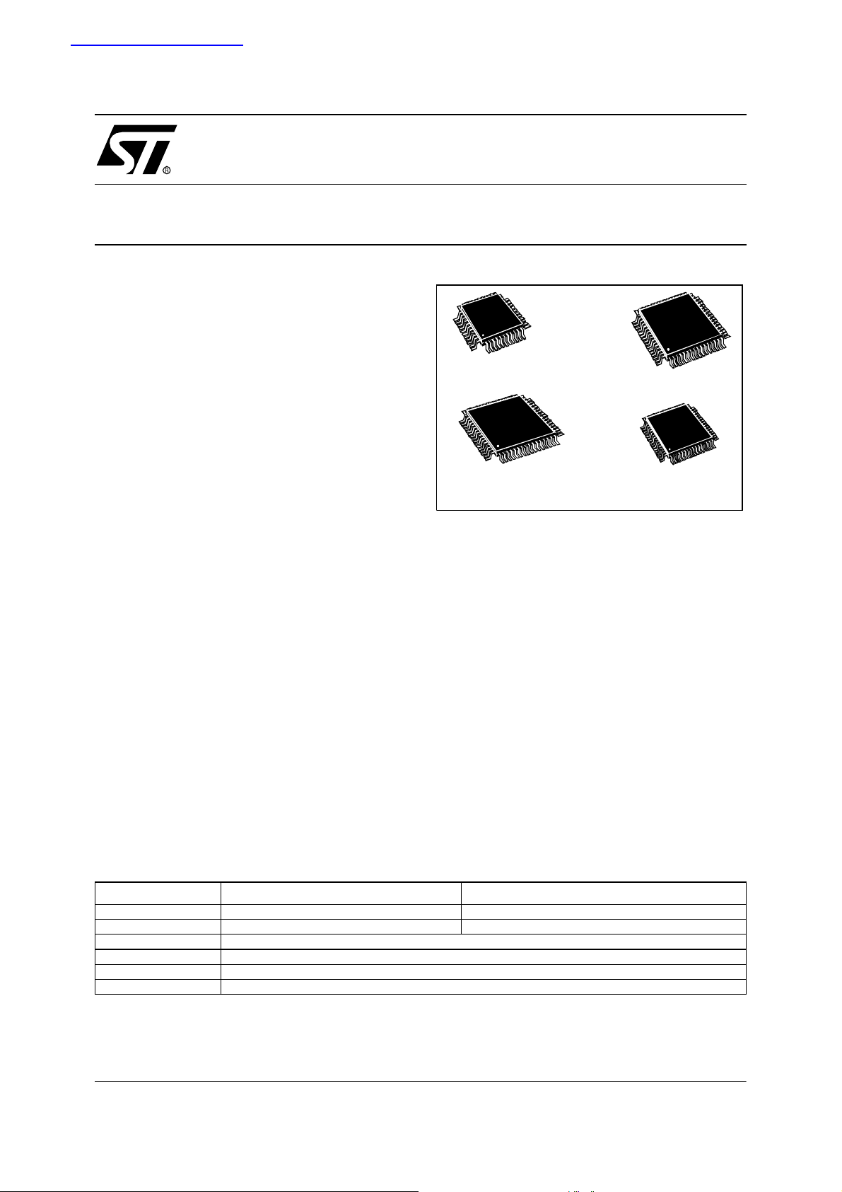
TQFP32
7x7mm
tion: 20 years at 55°C
■ Clock, Re set and Supp ly Managem ent
– Low power crystal/ceramic resona tor oscilla-
tors and bypass for external clock
– PLL for 2x frequency multiplication
– Five Power Saving Modes: Halt, Auto Wake
Up From Halt, Active-Halt, Wait and Slow
■ Interrupt Management
– Nested interrupt controller
– 14 interrupt vectors plus TRAP and RESET
– TLI top level interrupt (on 64-pin devices)
– Up to 21 external interrupt lines (on 4 vectors)
■ Up to 48 I/O Ports
– Up to 48 multifunctional bidirectional I/O lines
– Up to 36 alternate function lines
– Up to 6 high sink outputs
■ 5 Timers
– 16-bit Timer with: 2 input capt ures, 2 output
compares, external clock input, PWM and
pulse generator modes
– 8-bit Timer with: 1 or 2 input captures, 1 or 2
output compares, PWM and pu lse generator
modes
– 8-bit PWM Auto-Reload Time r with: 1 or 2 in-
put captures, 2 or 4 independent PWM output
channels, output compare and time base in-
terrupt, external clock with event detector
■ Up to 4 Communications Interfaces
■ Analog peripheral (low current coupling)
■ Instruction Set
TQFP44
10x10mm
– Main Clock Controller with: Real time base
and Clock output
– Window watchdog timer
– SPI synchronous serial interface
– Master/slave
interface
– Master-only
terface
– CAN 2.0B active
– 10-bit A/D Converter with up to 16 inputs
– Up to 9 robust ports (low current coupling)
– 8-bit data manipulation
– 63 basic instructions
– 17 main addressing modes
– 8 x 8 unsigned multiply instruction
■ Development Tools
– Full hardware/software development package
Device Summary
Features ST72(F)561(AR/R/J/K)9 ST72(F)561(AR/R/J/K)6
Program memory - bytes 60K 32K
RAM (stac k) - bytes 2K (256) 1K (256)
Operati ng S upply 4.5V to 5.5V
CPU Frequency External Resonator Osc. w/ PLLx2/8MHz
Max. Temp . Range -40°C to +125°C
Package s TQFP64 10x 10mm (AR), TQF P64 14x14 m m (R), TQFP44 10x10mm (J ), TQ F P32 7x7mm (K)
, ACTIVE CAN
PRELIMINARY DATA
LINSCI asynchronous serial
LINSCI asynchronous serial in-
ST72561
TQFP64
14 x 14
TQFP64
10 x 10
Rev. 2
May 2004 1/262
This is preliminary information on a new product now in development or undergoing evaluation. Details are subject to change without notice.
1
Page 2

Table of Contents
1 INTRODUCTION . . . . . . . . . . . . . . . . . . . . . . . . . . . . . . . . . . . . . . . . . . . . . . . . . . . . . . . . . . . . . . 5
2 PIN DESCRIPTION . . . . . . . . . . . . . . . . . . . . . . . . . . . . . . . . . . . . . . . . . . . . . . . . . . . . . . . . . . . . 6
3 REGISTER & MEMORY MAP . . . . . . . . . . . . . . . . . . . . . . . . . . . . . . . . . . . . . . . . . . . . . . . . . . . 12
4 FLASH PROGRAM MEMORY . . . . . . . . . . . . . . . . . . . . . . . . . . . . . . . . . . . . . . . . . . . . . . . . . . 16
4.1 INTRODUCTION . . . . . . . . . . . . . . . . . . . . . . . . . . . . . . . . . . . . . . . . . . . . . . . . . . . . . . . . 16
4.2 MAIN FEATURES . . . . . . . . . . . . . . . . . . . . . . . . . . . . . . . . . . . . . . . . . . . . . . . . . . . . . . . 16
4.3 STRUCTURE . . . . . . . . . . . . . . . . . . . . . . . . . . . . . . . . . . . . . . . . . . . . . . . . . . . . . . . . . . . 16
4.4 ICC INTERFACE . . . . . . . . . . . . . . . . . . . . . . . . . . . . . . . . . . . . . . . . . . . . . . . . . . . . . . . . 17
4.5 ICP (IN-CIRCUIT PROGRAMMING) . . . . . . . . . . . . . . . . . . . . . . . . . . . . . . . . . . . . . . . . . 18
4.6 IAP (IN-APPLICATION PROGRAMMING) . . . . . . . . . . . . . . . . . . . . . . . . . . . . . . . . . . . . . 18
4.7 RELATED DOCUMENTATION . . . . . . . . . . . . . . . . . . . . . . . . . . . . . . . . . . . . . . . . . . . . . 18
4.8 REGISTER DESCRIPTION . . . . . . . . . . . . . . . . . . . . . . . . . . . . . . . . . . . . . . . . . . . . . . . . 18
5 CENTRAL PROCESSING UNIT . . . . . . . . . . . . . . . . . . . . . . . . . . . . . . . . . . . . . . . . . . . . . . . . . 19
5.1 INTRODUCTION . . . . . . . . . . . . . . . . . . . . . . . . . . . . . . . . . . . . . . . . . . . . . . . . . . . . . . . . 19
5.2 MAIN FEATURES . . . . . . . . . . . . . . . . . . . . . . . . . . . . . . . . . . . . . . . . . . . . . . . . . . . . . . . 19
5.3 CPU REGISTERS . . . . . . . . . . . . . . . . . . . . . . . . . . . . . . . . . . . . . . . . . . . . . . . . . . . . . . . 19
6 SUPPLY, RESET AND CLOCK MANAGEMENT . . . . . . . . . . . . . . . . . . . . . . . . . . . . . . . . . . . . 22
6.1 PHASE LOCKED LOOP . . . . . . . . . . . . . . . . . . . . . . . . . . . . . . . . . . . . . . . . . . . . . . . . . . 22
6.2 MULTI-OSCILLATOR (MO) . . . . . . . . . . . . . . . . . . . . . . . . . . . . . . . . . . . . . . . . . . . . . . . . 23
6.3 RESET SEQUENCE MANAGER (RSM) . . . . . . . . . . . . . . . . . . . . . . . . . . . . . . . . . . . . . . 24
6.4 SYSTEM INTEGRITY MANAGEMENT (SI) . . . . . . . . . . . . . . . . . . . . . . . . . . . . . . . . . . . . 26
7 INTERRUPTS . . . . . . . . . . . . . . . . . . . . . . . . . . . . . . . . . . . . . . . . . . . . . . . . . . . . . . . . . . . . . . . 30
7.1 INTRODUCTION . . . . . . . . . . . . . . . . . . . . . . . . . . . . . . . . . . . . . . . . . . . . . . . . . . . . . . . . 30
7.2 MASKING AND PROCESSING FLOW . . . . . . . . . . . . . . . . . . . . . . . . . . . . . . . . . . . . . . . 30
7.3 INTERRUPTS AND LOW POWER MODES . . . . . . . . . . . . . . . . . . . . . . . . . . . . . . . . . . . 32
7.4 CONCURRENT & NESTED MANAGEMENT . . . . . . . . . . . . . . . . . . . . . . . . . . . . . . . . . . 32
7.5 INTERRUPT REGISTER DESCRIPTION . . . . . . . . . . . . . . . . . . . . . . . . . . . . . . . . . . . . . 33
7.6 EXTERNAL INTERRUPTS . . . . . . . . . . . . . . . . . . . . . . . . . . . . . . . . . . . . . . . . . . . . . . . . 36
8 POWER SAVING MODES . . . . . . . . . . . . . . . . . . . . . . . . . . . . . . . . . . . . . . . . . . . . . . . . . . . . . 39
8.1 INTRODUCTION . . . . . . . . . . . . . . . . . . . . . . . . . . . . . . . . . . . . . . . . . . . . . . . . . . . . . . . . 39
8.2 SLOW MODE . . . . . . . . . . . . . . . . . . . . . . . . . . . . . . . . . . . . . . . . . . . . . . . . . . . . . . . . . . . 39
8.3 WAIT MODE . . . . . . . . . . . . . . . . . . . . . . . . . . . . . . . . . . . . . . . . . . . . . . . . . . . . . . . . . . . 40
8.4 HALT MODE . . . . . . . . . . . . . . . . . . . . . . . . . . . . . . . . . . . . . . . . . . . . . . . . . . . . . . . . . . . 41
8.5 ACTIVE-HALT MODE . . . . . . . . . . . . . . . . . . . . . . . . . . . . . . . . . . . . . . . . . . . . . . . . . . . . 42
8.6 AUTO WAKE UP FROM HALT MODE . . . . . . . . . . . . . . . . . . . . . . . . . . . . . . . . . . . . . . . 44
9 I/O PORTS . . . . . . . . . . . . . . . . . . . . . . . . . . . . . . . . . . . . . . . . . . . . . . . . . . . . . . . . . . . . . . . . . . 47
9.1 INTRODUCTION . . . . . . . . . . . . . . . . . . . . . . . . . . . . . . . . . . . . . . . . . . . . . . . . . . . . . . . . 47
9.2 FUNCTIONAL DESCRIPTION . . . . . . . . . . . . . . . . . . . . . . . . . . . . . . . . . . . . . . . . . . . . . . 47
9.3 I/O PORT IMPLEMENTATION . . . . . . . . . . . . . . . . . . . . . . . . . . . . . . . . . . . . . . . . . . . . . . 50
9.4 LOW POWER MODES . . . . . . . . . . . . . . . . . . . . . . . . . . . . . . . . . . . . . . . . . . . . . . . . . . . 50
9.5 INTERRUPTS . . . . . . . . . . . . . . . . . . . . . . . . . . . . . . . . . . . . . . . . . . . . . . . . . . . . . . . . . . 50
9.6 I/O PORT IMPLEMENTATION . . . . . . . . . . . . . . . . . . . . . . . . . . . . . . . . . . . . . . . . . . . . . . 51
262
2/262
2
Page 3

Table of Contents
10 ON-CHIP PERIPHERALS . . . . . . . . . . . . . . . . . . . . . . . . . . . . . . . . . . . . . . . . . . . . . . . . . . . . . 54
10.1WINDOW WATCHDOG (WWDG) . . . . . . . . . . . . . . . . . . . . . . . . . . . . . . . . . . . . . . . . . . . 54
10.2MAIN CLOCK CONTROLLER WITH REAL TIME CLOCK MCC/RTC . . . . . . . . . . . . . . . 61
10.3PWM AUTO-RELOAD TIMER (ART) . . . . . . . . . . . . . . . . . . . . . . . . . . . . . . . . . . . . . . . . . 64
10.416-BIT TIMER . . . . . . . . . . . . . . . . . . . . . . . . . . . . . . . . . . . . . . . . . . . . . . . . . . . . . . . . . . 75
10.58-BIT TIMER (TIM8) . . . . . . . . . . . . . . . . . . . . . . . . . . . . . . . . . . . . . . . . . . . . . . . . . . . . . . 94
10.6SERIAL PERIPHERAL INTERFACE (SPI) . . . . . . . . . . . . . . . . . . . . . . . . . . . . . . . . . . . 112
10.7LINSCI SERIAL COMMUNICATION INT ERFACE (LIN MASTER/SL AVE) . . . . . . . . . . . 124
10.8LINSCI SERIAL COMMUNICATION INTERFACE (LIN MASTER ONLY) . . . . . . . . . . . . 155
10.9BECAN CONTROLLER (BECAN) . . . . . . . . . . . . . . . . . . . . . . . . . . . . . . . . . . . . . . . . . . 172
10.1010-BIT A/D CONVERTER (ADC) . . . . . . . . . . . . . . . . . . . . . . . . . . . . . . . . . . . . . . . . . . 211
11 INSTRUCTION SET . . . . . . . . . . . . . . . . . . . . . . . . . . . . . . . . . . . . . . . . . . . . . . . . . . . . . . . . 215
11.1CPU ADDRESSING MODES . . . . . . . . . . . . . . . . . . . . . . . . . . . . . . . . . . . . . . . . . . . . . . 215
11.2INSTRUCTION GROUPS . . . . . . . . . . . . . . . . . . . . . . . . . . . . . . . . . . . . . . . . . . . . . . . . 218
12 ELECTRICAL CHARACTERISTICS . . . . . . . . . . . . . . . . . . . . . . . . . . . . . . . . . . . . . . . . . . . . 221
12.1PARAMETER CONDITIONS . . . . . . . . . . . . . . . . . . . . . . . . . . . . . . . . . . . . . . . . . . . . . . 221
12.2ABSOLUTE MAXIMUM RATINGS . . . . . . . . . . . . . . . . . . . . . . . . . . . . . . . . . . . . . . . . . . 222
12.3OPERATING CONDITIONS . . . . . . . . . . . . . . . . . . . . . . . . . . . . . . . . . . . . . . . . . . . . . . . 223
12.4SUPPLY CURRENT CHARACTERISTICS . . . . . . . . . . . . . . . . . . . . . . . . . . . . . . . . . . . 225
12.5CLOCK AND TIMING CHARACTERISTICS . . . . . . . . . . . . . . . . . . . . . . . . . . . . . . . . . . 229
12.6AUTO WAKEUP FROM HALT OSCILLATOR (AWU) . . . . . . . . . . . . . . . . . . . . . . . . . . . 232
12.7MEMORY CHARACTERISTICS . . . . . . . . . . . . . . . . . . . . . . . . . . . . . . . . . . . . . . . . . . . 233
12.8EMC CHARACTERISTICS . . . . . . . . . . . . . . . . . . . . . . . . . . . . . . . . . . . . . . . . . . . . . . . 234
12.9I/O PORT PIN CHARACTERISTICS . . . . . . . . . . . . . . . . . . . . . . . . . . . . . . . . . . . . . . . . 236
12.10CONTROL PIN CHARACTERISTICS . . . . . . . . . . . . . . . . . . . . . . . . . . . . . . . . . . . . . . 241
12.11TIMER PERIPHERAL CHARACTERISTICS . . . . . . . . . . . . . . . . . . . . . . . . . . . . . . . . . 243
12.12COMMUNICATION INTERFACE CHARACTERISTICS . . . . . . . . . . . . . . . . . . . . . . . . 244
12.1310-BIT ADC CHARACTERISTICS . . . . . . . . . . . . . . . . . . . . . . . . . . . . . . . . . . . . . . . . . 246
13 PACKAGE CHARACTERISTICS . . . . . . . . . . . . . . . . . . . . . . . . . . . . . . . . . . . . . . . . . . . . . . 250
13.1PACKAGE MECHANICAL DATA . . . . . . . . . . . . . . . . . . . . . . . . . . . . . . . . . . . . . . . . . . . 250
13.2THERMAL CHARACTERISTICS . . . . . . . . . . . . . . . . . . . . . . . . . . . . . . . . . . . . . . . . . . . 252
13.3SOLDERING AND GLUEABILITY INFORMATION . . . . . . . . . . . . . . . . . . . . . . . . . . . . . 253
14 DEVICE CONFIGURATION AND ORDERING INFORMATION . . . . . . . . . . . . . . . . . . . . . . . 254
14.1FLASH OPTION BYTES . . . . . . . . . . . . . . . . . . . . . . . . . . . . . . . . . . . . . . . . . . . . . . . . . 254
14.2DEVICE ORDERING INFORMATION AND TRANSFER OF CUSTOMER CODE . . . . . 256
14.3DEVELOPMENT TOOLS . . . . . . . . . . . . . . . . . . . . . . . . . . . . . . . . . . . . . . . . . . . . . . . . . 258
15 IMPORTANT NOTES . . . . . . . . . . . . . . . . . . . . . . . . . . . . . . . . . . . . . . . . . . . . . . . . . . . . . . . 259
15.1CLEARING ACTIVE INTERRUPTS OUTSIDE INTERRUPT ROUTINE . . . . . . . . . . . . . 259
15.2CAN FIFO CORRUPTION . . . . . . . . . . . . . . . . . . . . . . . . . . . . . . . . . . . . . . . . . . . . . . . . 259
15.3FLASH/FASTROM DEVICES ONLY . . . . . . . . . . . . . . . . . . . . . . . . . . . . . . . . . . . . . . . . 259
15.4ROM DEVICES ONLY . . . . . . . . . . . . . . . . . . . . . . . . . . . . . . . . . . . . . . . . . . . . . . . . . . . 260
3/262
Page 4

Table of Contents
16 REVISION HISTORY . . . . . . . . . . . . . . . . . . . . . . . . . . . . . . . . . . . . . . . . . . . . . . . . . . . . . . . . 261
4/262
262
Page 5
1 INTRODUCTION
ST72561
The ST72561/ST72563 devices are members of
the ST7 microcontroller fam ily designed for midrange applications with CAN (Controller Area Network) and LIN (Local Interconnect Network) interface.
All devices are based on a common industrystandard 8-bit core, featuring an enhanced instruction set and are available with FLASH or ROM program memory.
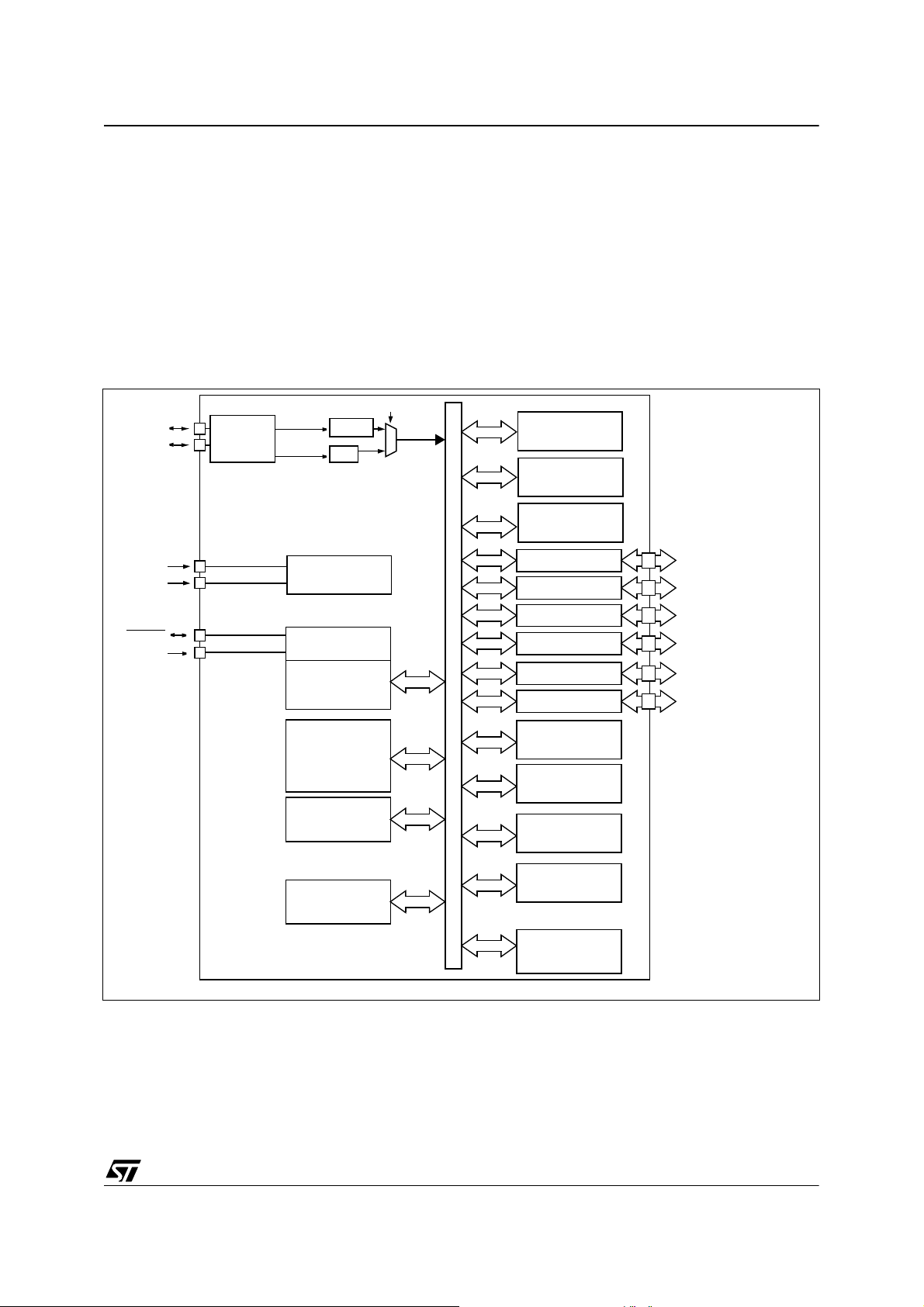
Figure 1. Device Block Diagram
option
OSC1
OSC2
V
DD
V
SS
RESET
1
TLI
OSC
PLL x 2
/2
POWER
SUPPLY
CONTROL
8-BIT CO RE
ALU
The enhanced instruction set and addressing
modes of the ST7 offer both power and flexibility to
software developers, enabling the design of highly
efficient and compact application code. In addition
to standard 8-bit data management, all ST7 microcontrollers feature true bit manipulation, 8x8 unsigned multiplication and indirect addressing
modes.
PWM
ART
8-bit
TIMER
16-Bit
TIMER
PA7:0
PORT A
PORT B
ADDRESS AND DATA BUS
PORT C
PORT D
PORT E
PORT F
(8 bits)
PB7:0
(8 bits)
PC7:0
(8 bits)
PD7:0
(8 bits)
PE7:0
(8 bits)
PF7:0
(8 bits)
1
1
1
1
1
1
PROGRAM
MEMORY
(16 - 60 K Bytes)
RAM
(512 - 204 8 Bytes)
MCC
(Clock C ont rol)
SPI
LINSCI2
(LIN master)
LINSCI1
(LIN master/slave)
CAN
(2.0B ACTIVE)
WINDOW
WATCHDOG
1
On some devices only, see Device Summary on page 1
3
5/262
Page 6
ST72561
2 PIN DESCRI PTION
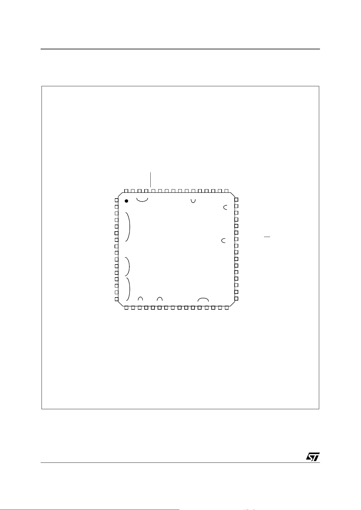
Figure 2. TQFP 64-Pin Package Pinout
LINSCI2_SCK
OSC1
OSC2
ARTIC1 / PA0
PWM0 / PA1
PWM1 / (HS) PA2
PWM2 / PA3
PWM3 / PA4
V
SS_3
V
DD_3
ARTCLK / (HS)PA5
ARTIC2 / (HS) PA6
T8_OCMP2 / PA7
T8_ICAP2 / PB0
T8_OCMP1 / PB1
T8_ICAP1 / PB2
MCO / PB3
PF7
PF6
PD7 / AIN11
PD6 / AIN10
RESET
DD_0VDDAVSS_0VSSA
V
PD5 / LINSCI2_TDO
PF5
TLI
PD3 (HS)/
PD4 / LINSCI2_RDI
64 63 62 61 60 59 58 57 56 55 54 53 52 51 50 49
1
2
ei3
ei3
ei3
3
4
ei0
5
6
7
ei3
8
9
10
ei0
11
12
13
14
ei1
15
ei1
16
17 18 19 20 21 22 23 24 29 30 31 3225 26 27 28
AIN13 / PE1
AIN12 / PE0
ICCCLK / AIN0 / PB4
AIN14 / PE2
ei1
AIN15 / PE3
ICCDATA / AIN1 / PB5
(*)T16_OCMP1 / AIN2 / PB6
ei2
SS_2
DD_2
V
V
(*)T16_ICAP1 / AIN4 / PC0
(*)T16_OCMP2 / AIN3 / PB7
PE4
T16_EXTCLK / (HS) PC2
(*)T16_ICAP2 / (H S) PC1
PF4
PF3 / AIN9
PD2 /
48
47
46
45
44
43
42
41
40
39
38
37
36
35
34
33
PP
NC
ICCSEL/V
(HS) 20mA high sink cap ability
LINSCI1_TDO
PD1 /
LINSCI1_RDI
PF2 / AIN8
PF1 / AIN7
PF0
PE7
PD0 / SPI_SS
V
_1
DD
V
_1
SS
/ AIN6
PC7 / SPI_SCK
PC6 / SPI_MOSI
PC5 / SPI_MISO
PE6 / AIN5
PE5
PC4 / CAN_TX
PC3 / CAN_RX
eix associated external interrupt vector
(*) : by option bit:
T16_ICAP 1 can be moved to PD 4
T16_ICAP 2 can be moved to PD 1
T16_OCMP 1 can be moved to PD 3
T16_OCMP 2 can be moved to PD 5
6/262
Page 7
PIN DESCRIPTION (Cont’d)
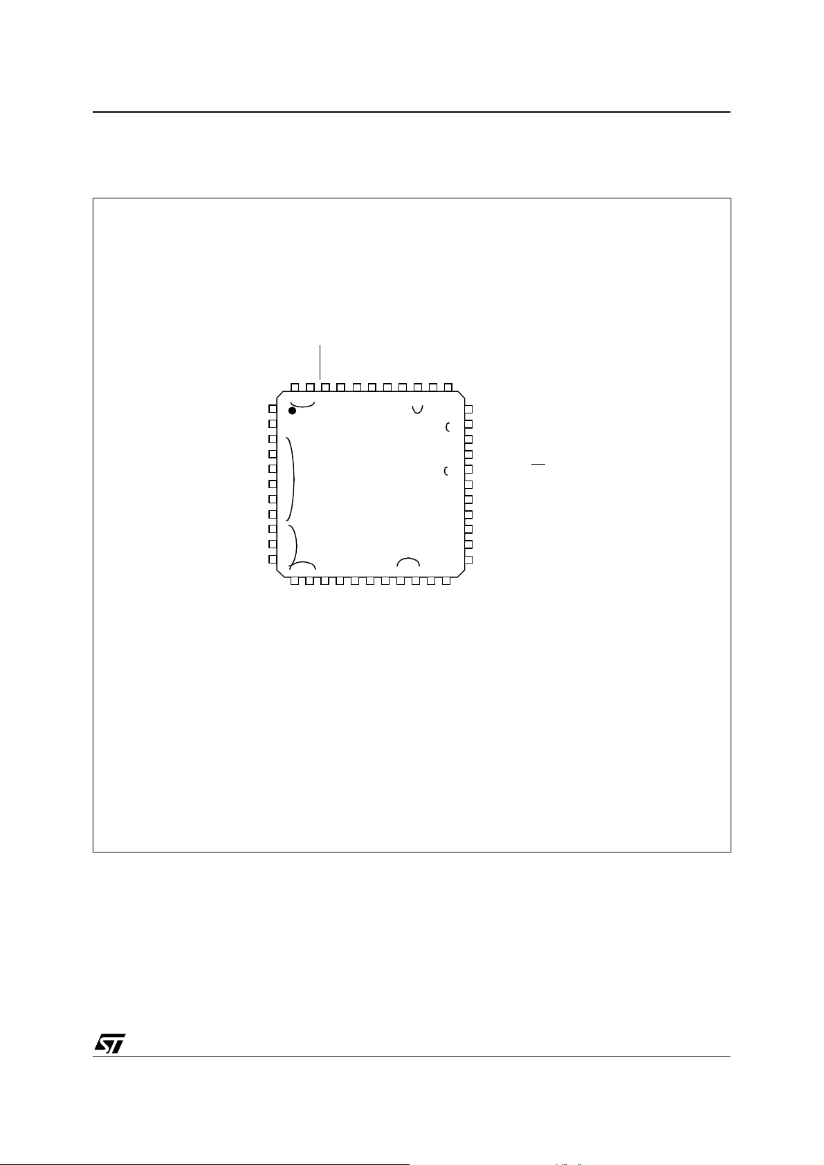
Figure 3. TQFP 44-Pin Package Pinout
PD7 / AIN11
PD6 / AIN10
RESET
OSC1
OSC2
PWM0 / PA1
PWM1 / (HS) PA2
PWM2 / PA3
PWM3 / PA4
ARTCLK / (HS)PA5
ARTIC2 / (HS) PA6
T8_OCMP1 / PB1
T8_ICAP1 / PB2
MCO / PB3
44 43 42 41 40 39 38 37 36 35 34
1
ei3
2
3
4
5
ei0
6
7
8
9
ei1
10
ei1
11
12 13 14 15 16 17 18 19 20 21 22
1
PD5 / LINSCI2_TDO
DD_0VDDAVSS_0VSSA
V
ei2
ei3
ST72561
LINSCI2_SCK
PD4 / LINSCI2_RDI
PD3 (HS) /
PF5
PD2 /
LINSCI1_TDO
PD1 /
LINSCI1_RDI
PF2 / AIN8
PF1 / AIN7
PD0 / SPI_SS
/ AIN6
PC7 / SPI_SCK
PC6 / SPI_MOSI
PC5 / SPI_MISO
PE6 / AIN5
PC4 / CAN_TX
PC3 / CAN_RX
ei3
ei3
33
32
31
30
29
28
27
26
25
24
23
ICCCLK / AIN0 / PB4
ICCDATA / AIN1 / PB5
(*)T16_OCMP1 / AIN2 / PB6
SS_2
DD_2
V
V
PP
PE4
ICCSEL/V
(HS) 20mA high sink capability
eix associatedexternal interrupt vector
(*)T16_OCMP2 / AIN3 / PB7
T16_EXTCLK / (HS) PC2
(*)T16_ICAP2 / (H S) PC1
(*)T16_ICAP1 / AIN4 / PC0
(*) : by option bit:
T16_I CA P1 can be mo ved to PD4
T16_I CA P2 can be mo ved to PD1
T16_OCMP1 can be moved to PD3
T16_OCMP2 can be moved to PD5
7/262
Page 8

ST72561
PIN DESCRIPTION (Cont’d)
Figure 4. TQFP 32-Pin Package Pinout
OSC1
OSC2
PWM0 / PA1
PWM1 / (HS) PA2
ARTCLK / (HS) PA5
T8_OCMP1 / PB1
T8_ICAP1 / PB2
MCO / PB3
32 31 30 29 28 27 26 25
1
2
3
4
5
6
7
8
9 10111213141516
RESET
ei0
ei1
ei1
PD5 / LINSCI2_TDO
DD_0VDDA
V
SS_0VSSA
V
ei3
ei2
ei3
1
LINSCI2_SCK
PD4 / LINSCI2_RDI
PD3 (HS) /
PD2 /
24
23
22
21
20
19
18
17
LINSCI1_TDO
LINSCI1_RDI
PD1 /
PD0 / SPI_SS
/ AIN6
PC7 / SPI_SCK
PC6 / SPI_MOSI
PC5 / SPI_MISO
PC4 / CAN_TX
PC3 / CAN_RX
PP
ICCSEL/V
ICCCLK / AIN0 / PB4
ICCDATA / AIN1 / PB5
T16_OCMP 1 / AIN 2 / PB6
T16_OCMP2 / AIN3 / PB7
T16_ICAP2 / (HS) PC1
T16_ICAP1 / AIN4 / PC0
T16_EXTCLK / (HS) PC2
(HS) 20mA high sink capability
eix associated external interrupt vector
(*) : by option bit:
T16_ICAP 1 can be moved t o PD 4
T16_ICAP 2 can be moved t o PD 1
T16_OCMP 1 can be moved to PD 3
T16_OCMP 2 can be moved to PD 5
For external pin connection guidelines, refer to See “ELECTRICAL CHARACTERISTICS” on page 221.
8/262
Page 9
ST72561
PIN DESCRIPTION (Cont’d)
For external pin connection guidelines, refer to See “ELECTRICAL CHARACTERISTICS” on page 221.
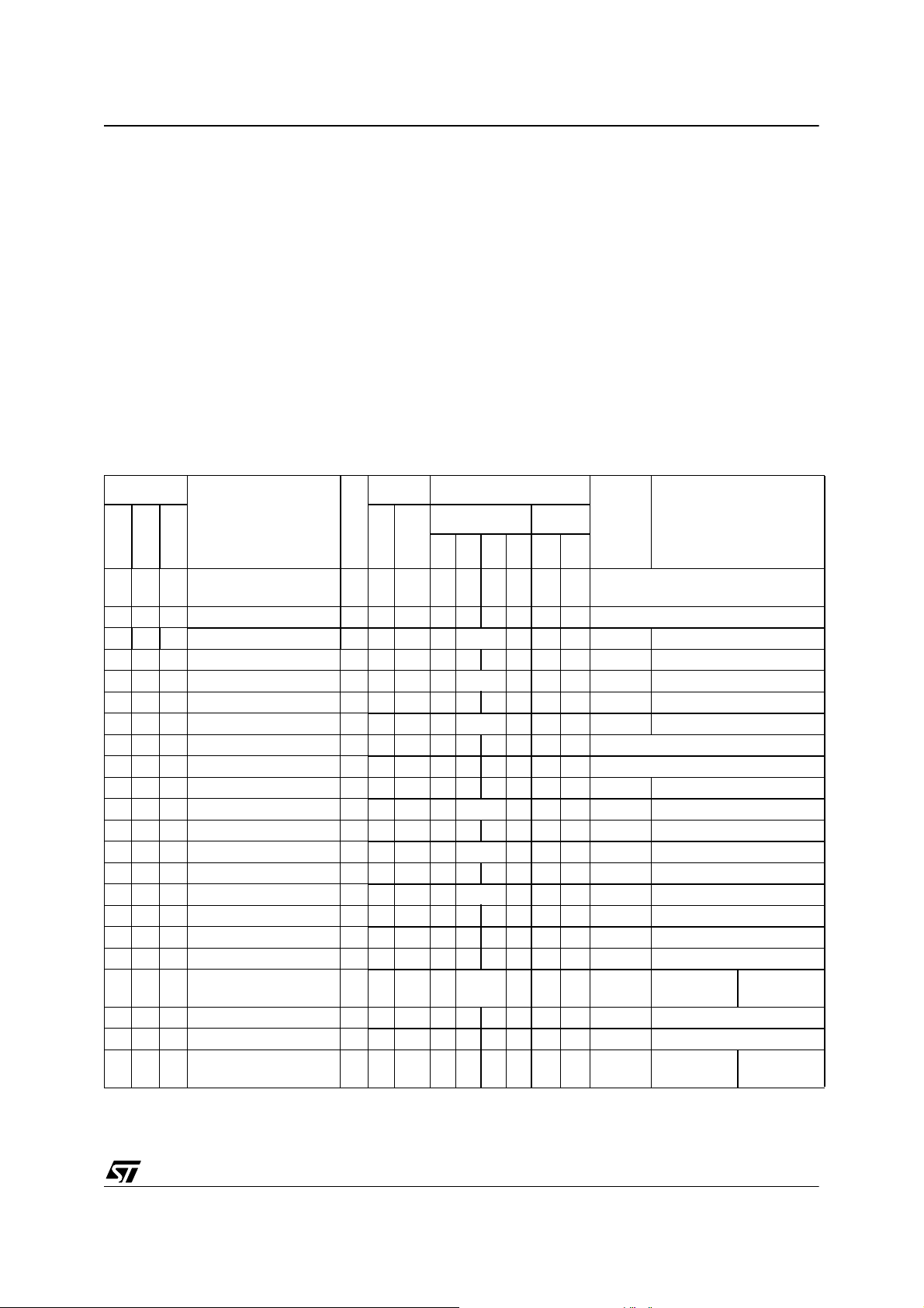
Legend / Abbreviations for Tab le 1:
Type: I = input, O = output, S = supply
In/Output le v el: C
Output level: HS = 20mA high sink (on N-buffer only)
Port and control configuration:
– Input: float = floating, wpu = weak pull-up, int = interrupt
– Output: OD = open drain, PP = push-pull
Refer to “I/O PORTS” on page 47 for more details on the software configuration of the I/O ports.
The RESET con figur atio n of each pin is shown i n bol d whic h i s valid as long as the devi ce is i n rese t sta te .
Table 1. Device Pin Description
= CMOS 0.3VDD/0.7VDD with Schmitt trigger
T
T
= TTL 0.8V / 2V with Schmitt trigger
T
1)
, ana = analog, RB = robust
Pin n°
Pin Name
Type
TQFP64
TQFP44
TQFP32
111OSC1
222OSC2
3)
3)
I
I/O Resonator oscillator inverter output
3 - - PA0 / ARTIC1 I/O C
4 3 3 PA1 / PWM0 I/O C
5 4 4 PA2 (HS) / PWM1 I/O C
6 5 - PA3 / PWM2 I/O C
7 6 - PA4 / PWM3 I/O C
8--V
9--V
SS_3
DD_3
S Digital Ground Voltage
S Digital Main Supply Voltage
10 7 5 PA5 (HS) / ARTCLK I/O C
11 8 - PA6 (HS) / ARTIC2 I/O C
12 - - PA7 / T8_OCMP2 I/O C
13 - - PB0 /T8_ICAP2 I/O C
14 9 6 PB1 /T8_OCMP1 I/O C
15 10 7 PB2 / T8_ICAP1 I/O C
16 11 8 PB3 / MCO I/O C
17 - - PE0 / AIN12 I/O T
18 - - PE1 / AIN13 I/O T
19 12 9 PB4 / AIN0 / ICCCLK I/O C
20 - - PE2 / AIN14 I/O T
21 - - PE3 / AIN15 I/O T
22 13 10 PB5 / AIN1 / ICCDATA I/O C
Level Port
Input Output
Input
Output
float
int
wpu
OD
ana
function
(after
reset)
PP
Main
Alternate function
External clock input or Resonator oscillator inverter input
T
T
T
T
T
T
T
T
T
T
T
T
T
T
T
T
T
T
X ei0 X X Port A0 ART Input Capture 1
X ei0 X X Port A1 ART PWM Output 0
HS X ei0 X X Port A2 ART PWM Output 1
X ei0 X X Port A3 ART PWM Output 2
X ei0 X X Port A4 ART PWM Output 3
HS X ei0 X X Port A5 ART External Clock
HS X ei0 X X Port A6 ART Input Capture 2
X ei0 X X Port A7 TIM8 Output Compare 2
X ei1 X X Port B0 TIM8 Input Capture 2
X ei1 X X Port B1 TIM8 Output Compare 1
X ei1 X X Port B2 TIM8 Input Capture 1
X ei1 X X Port B3 Main clock out (f
X X RB X X Port E0 ADC Analog Input 12
X X RB X X Port E1 ADC Analog Input 13
X ei1 RB X X Port B4
ICC Clock
input
X X RB X X Port E2 ADC Analog Input 14
X X RB X X Port E3 ADC Analog Input 15
X ei1 RB X X Port B5
ICC Data input
)
OSC2
ADC Analog
Input 0
ADC Analog
Input 1
9/262
Page 10

ST72561
Pin n°
Pin Name
TQFP64
TQFP44
TQFP32
23 14 11
24 15 - V
25 16 - V
26 17 12
27 18 13
PB6 / AIN2 /
T16_OCMP1
SS_2
DD_2
PB7 /AIN3 /
T16_OCMP2
PC0 / AIN4 /
T16_ICAP1
28 19 14 PC1 (HS) / T16_ICAP2 I/O C
29 20 15
PC2 (HS) /
T16_EXTCLK
30 21 - PE4 I/O T
Level Port
Type
Input
Output
I/O C
T
Input Output
float
int
wpu
OD
ana
X XRBXXPort B6
function
(after
reset)
PP
Main
S Digital Ground Voltage
S Digital Main Supply Voltage
I/O C
I/O C
I/O C
T
T
T
T
T
X XRBXXPort B7
X XRBXXPort C0
HS X ei2 X X Port C1 TIM16 Input Capture 2
HS X ei2 X X Port C2 TIM16 External Clock input
X XXXPort E4
31 - - NC Not Connected
32 22 16 V
PP
I
33 23 17 PC3 / CANRX I/O C
34 24 18 PC4 / CANTX I/O C
35 - - PE5 I/O T
36 25 - PE6 / AIN5 I/O T
37 26 19 PC5 /MISO I/O C
38 27 20 PC6 / MOSI I/O C
39 28 21 PC7 /SCK I/O C
40 - - V
41 - - V
SS_1
DD_1
42 29 22 PD0 / SS
/ AIN6 I/O C
S Digital Ground Voltage
S Digital Main Supply Voltage
43 - - PE7 I/O T
44 - - PF0 I/O T
45 30 - PF1 / AIN7 I/O T
46 31 - PF2 / AIN8 I/O T
47 32 23 PD1 / SCI1_RDI I/O C
48 33 24 PD2 / SCI1_TDO I/O C
49 - - PF3 / AIN9 I/O T
50 - - PF4 I/O T
51 - - TLI I C
52 34 - PF5 I/O T
53 35 25 PD3 (HS) / SCI2_SCK I/O C
54 36 26 PD4 / SCI2_RDI I/O C
T
T
T
T
T
T
T
T
T
T
T
T
T
T
T
T
T
T
T
T
X X X X Port C3 CAN Receive Data Input
X X2)Port C4 CAN Transmit Data Output
X XXXPort E5
X X X X X Port E6 ADC Analog Input 5
X X X X Port C5 SPI Master In/Slave Out
X X X X Port C6 SPI Master Out/Slave In
X X X X Port C7 SPI Serial Clock
X ei3 X X X Port D0
X XXXPort E7
X XXXPort F0
X X X X X Port F1 ADC Analog Input 7
X X X X X Port F2 ADC Analog Input 8
X ei3 X X Port D1 LINSCI1 Receive Data input
X XXXPort D2
X X X X X Port F3 ADC Analog Input 9
X XXXPort F4
X X Top level interrupt input pin
X XXXPort F5
HS X XXXPort D3
X ei3 X X Port D4 LINSCI2 Receive Data input
Flash programming voltage.Must be
tied low in user mode
Alternate function
TIM16 Output Compare
1
TIM16 Output Compare
2
TIM16 Input
Capture 1
SPI Slave
Select
LINSCI1 Transmit Data out-
ADC Analog
Input 2
ADC Analog
Input 3
ADC Analog
Input 4
ADC Analog
Input 6
put
LINSCI2 Serial Clock Out-
put
10/262
Page 11

ST72561
Pin n°
Pin Name
TQFP64
TQFP44
TQFP32
55 37 27 V
56 38 28 V
57 39 29 V
58 40 30 V
SSA
SS_0
DDA
DD_0
59 41 31 PD5 / SCI2_TDO I/O C
60 42 32 RESET
61 43 - PD6 / AIN10 I/O C
62 44 - PD7 / AIN11 I/O C
63 - - PF6 I/O T
64 - - PF7 I/O T
Level Port
Type
Input
Output
float
Input Output
int
wpu
OD
ana
function
(after
reset)
PP
Main
Alternate function
S Analog Ground Voltage
S Digital Ground Voltage
I Analog Reference Voltage for ADC
S Digital Main Supply Voltage
LINSCI2 Transmit Data out-
put
I/O C
T
T
T
T
T
T
X XXXPort D5
Top priority non maskable interrupt.
X ei3 X X X Port D6 ADC Analog Input 10
X ei3 X X X Port D7 ADC Analog Input 11
X XXXPort F6
X XXXPort F7
Notes:
1. In the interrupt input column, “eiX ” defines the associated ex ternal in terrupt vecto r. If the weak pul l-up
column (wpu) is merged with the interrupt column (int), then the I/O configuration is pull-up interrupt input,
else the configuration is floating interrupt input.
2. Input mode can be used for general purpose I/O, output mode only for CANTX.
3. OSC1 and OSC2 p ins c onnect a cry stal/ceram ic resonator, or an external source to t he on-chi p os cillator; see Section 1 and Section 12.5 "CLOCK AND TIMING CHARACTERISTICS" for more details.
4. On the chip, each I/O port has 8 pads. Pads that are not bonded to external pins are in input pull-up configuration after reset. The c onfiguration of th ese pads must be kept at reset st at e to av oi d ad ded c urrent
consumption.
11/262
Page 12

ST72561
3 REGISTER & MEMORY MAP
As sho wn in Figure 5, the MCU is capable of addressing 64K bytes of memories and I/O registers.
The available memory locations consist of 128
bytes of register locations, up to 2 Kbytes of RA M
and up to 60 Kbytes of user program memory.
Figure 5. Me m ory Map
0000h
007Fh
0080h
087Fh
0880h
0FFFh
1000h
FFDFh
FFE0h
FFFFh
HW Registers
(see Table 2)
RAM
(2048/1024/
512 Bytes)
Reserved
Program Memory
(60K, 32K,16K)
Interrupt & Reset Vectors
(see Table 8)
0080h
00FFh
0100h
01FFh
0200h
027Fh
or 047Fh
or 087Fh
The RAM space includes up to 256 byt es for the
stack from 0100h to 01FFh.Th e highest address
bytes contain the user reset and interrupt vectors.
IMPORTANT: Memory locations marked as “Re-
served” must never be ac ces sed. Ac cessi ng a reseved area can have unpredictable e ffects on the
device.
Short Addressing
RAM (zero page)
256 Bytes Stack
16-bit Addressing
RAM
1000h
60 KBytes
8000h
32 KBytes
C000h
16 KBytes
FFDFh
Table 2. Hardware Register Map
Address Block
0000h
0001h
Port A
0002h
0003h
0004h
Port B
0005h
0006h
0007h
Port C
0008h
0009h
000Ah
Port D
000Bh
000Ch
000Dh
Port E
000Eh
12/262
Register
Label
PADR
PADDR
PAOR
PBDR
PBDDR
PBOR
PCDR
PCDDR
PCOR
PDDR
PDDDR
PDOR
PEDR
PEDDR
PEOR
Register Name
Port A Data Register
Port A Data Direction Register
Port A Option Register
Port B Data Register
Port B Data Direction Register
Port B Option Register
Port C Data Register
Port C Data Direction Register
Port C Option Register
Port D Data Register
Port D Data Direction Register
Port D Option Register
Port E Data Register
Port E Data Direction Register
Port E Option Register
Reset
Status
1)
00h
00h
00h
1)
00h
00h
00h
1)
00h
00h
00h
1)
00h
00h
00h
1)
00h
00h
00h
Remarks
2)
R/W
2)
R/W
2)
R/W
2)
R/W
2)
R/W
2)
R/W
2)
R/W
2)
R/W
2)
R/W
2)
R/W
2)
R/W
2)
R/W
2)
R/W
2)
R/W
2)
R/W
Page 13

ST72561
Address Block
000Fh
0010h
Port F
0011h
Register
Label
PFDR
PFDDR
PFOR
Register Name
Port F Data Register
Port F Data Direction Register
Port F Option Register
Reset
Status
1)
00h
00h
00h
0012h
to
Reserved Area (15 Bytes)
0020h
0021h
0022h
0023h
SPI
SPIDR
SPICR
SPICSR
SPI Data I/O Register
SPI Control Register
SPI Control/Status Register
xxh
0xh
00h
0024h FLASH FCSR Flash Control/Sta tus Registe r 00h R/W
0025h
0026h
0027h
0028h
0029h
002Ah
002Bh
002Ch
002Dh
002Eh
ITC
AWU
CKCTRL
ISPR0
ISPR1
ISPR2
ISPR3
EICR0
EICR1
AWUCSR
AWUPR
SICSR
MCCSR
Interrupt Software Priority Register 0
Interrupt Software Priority Register 1
Interrupt Software Priority Register 2
Interrupt Software Priority Register 3
External Interrupt Control Register 0
External Interrupt Control Register 1
Auto Wake up f. Halt Control/Status Register
Auto Wake Up From Halt Prescaler
System Integrity Control / Status Register
Main Clock Control / Status Register
FFh
FFh
FFh
FFh
00h
00h
00h
FFh
0xh
00h
Remarks
2)
R/W
2)
R/W
2)
R/W
R/W
R/W
R/W
R/W
R/W
R/W
R/W
R/W
R/W
R/W
R/W
R/W
R/W
002Fh
0030h
0031h
0032h
0033h
0034h
0035h
0036h
0037h
0038h
0039h
003Ah
003Bh
003Ch
003Dh
003Eh
003Fh
0040h
0041h
0042h
0043h
0044h
0045h
0046h
0047h
WWDG
PWM
ART
8-BIT
TIMER
ADC
WDGCR
WWDGR
PWMDCR3
PWMDCR2
PWMDCR1
PWMDCR0
PWMCR
ARTCSR
ARTCAR
ARTARR
ARTICCSR
ARTICR1
ARTICR2
T8CR2
T8CR1
T8CSR
T8IC1R
T8OC1R
T8CTR
T8ACTR
T8IC2R
T8OC2R
ADCCSR
ADCDRH
ADCDRL
Watchdog Control Register
Window Watchdog Register
Pulse Width Modulator Duty Cycle Register 3
PWM Duty Cycle Register 2
PWM Duty Cycle Register 1
PWM Duty Cycle Register 0
PWM Control register
Auto-Reload Timer Control/Status Register
Auto-Reload Timer Counter Access Register
Auto-Reload Timer Auto-Reload Register
ART Input Capture Control/Status Register
ART Input Capture Register 1
ART Input Capture register 2
Timer Control Register 2
Timer Control Register 1
Timer Control/Sta tus Registe r
Timer Input Capture 1 Register
Timer Output Compare 1 Register
Timer Counter Registe r
Timer Alternate Counter Register
Timer Input Capture 2 Register
Timer Output Compare 2 Register
Control/Status Register
Data High Register
Data Low Register
7Fh
7Fh
00h
00h
00h
00h
00h
00h
00h
00h
00h
00h
00h
00h
00h
00h
xxh
00h
FCh
FCh
xxh
00h
00h
00h
00h
R/W
R/W
R/W
R/W
R/W
R/W
R/W
R/W
R/W
R/W
R/W
Read Only
Read Only
R/W
R/W
Read Only
Read Only
R/W
Read Only
Read Only
Read Only
R/W
R/W
Read Only
Read Only
13/262
Page 14

ST72561
Address Block
0048h
0049h
004Ah
004Bh
004Ch
004Dh
LINSCI1
(LIN Master/
Slave)
004Eh
004Fh
Register
Label
SCI1ISR
SCI1DR
SCI1BRR
SCI1CR1
SCI1CR2
SCI1CR3
SCI1ERPR
SCI1ETPR
Register Name
SCI1 Status Register
SCI1 Data Register
SCI1 Baud Rate Register
SCI1 Control Register 1
SCI1 Control Register 2
SCI1Control Register 3
SCI1 Extended Receive Prescaler Register
SCI1 Extended Transmit Prescaler Register
0050h Reserved Area (1 Byte)
0051h
0052h
0053h
0054h
0055h
0056h
0057h
0058h
0059h
005Ah
005Bh
005Ch
005Dh
005Eh
005Fh
16-BIT
TIMER
T16CR2
T16CR1
T16CSR
T16IC1HR
T16IC1LR
T16OC1HR
T16OC1LR
T16CHR
T16CLR
T16ACHR
T16ACLR
T16IC2HR
T16IC2LR
T16OC2HR
T16OC2LR
Timer Control Register 2
Timer Control Register 1
Timer Control/Sta tus Registe r
Timer Input Capture 1 High Register
Timer Input Capture 1 Low Register
Timer Output Compare 1 High Register
Timer Output Compare 1 Low Register
Timer Counter High Register
Timer Counter Low Register
Timer Alternate Counter High Register
Timer Alternate Counter Low Register
Timer Input Capture 2 High Register
Timer Input Capture 2 Low Register
Timer Output Compare 2 High Register
Timer Output Compare 2 Low Register
Reset
Status
C0h
xxh
00h
xxh
00h
00h
00h
00h
00h
00h
00h
xxh
xxh
80h
00h
FFh
FCh
FFh
FCh
xxh
xxh
80h
00h
Remarks
Read Only
R/W
R/W
R/W
R/W
R/W
R/W
R/W
R/W
R/W
R/W
Read Only
Read Only
R/W
R/W
Read Only
Read Only
Read Only
Read Only
Read Only
Read Only
R/W
R/W
0060h
0061h
0062h
0063h
0064h
0065h
0066h
0067h
LINSCI2
(LIN Master)
SCI2SR
SCI2DR
SCI2BRR
SCI2CR1
SCI2CR2
SCI2CR3
SCI2ERPR
SCI2ETPR
SCI2 Status Register
SCI2 Data Register
SCI2 Baud Rate Register
SCI2 Control Register 1
SCI2 Control Register 2
SCI2 Control Register 3
SCI2 Extended Receive Prescaler Register
SCI2 Extended Transmit Prescaler Register
C0h
xxh
00h
xxh
00h
00h
00h
00h
Read Only
R/W
R/W
R/W
R/W
R/W
R/W
R/W
14/262
Page 15

ST72561
Address Block
0068h
0069h
006Ah
006Bh
006Ch
006Dh
006Eh
006Fh
0070h
0071h
0072h
0073h
0074h
0075h
0076h
0077h
0078h
0079h
007Ah
007Bh
007Ch
007Dh
007Eh
007Fh
Active CAN
Register
Label
CMCR
CMSR
CTSR
CTPR
CRFR
CIER
CDGR
CPSR
PAGES
Register Name
CAN Master Control Register
CAN Master Status Register
CAN Transmit Status Register
CAN Transmit Priority Register
CAN Receive FIFO Register
CAN Interrupt Enable Register
CAN Diagnosis Register
CAN Page Selection Register
PAGE REGISTER 0
PAGE REGISTER 1
PAGE REGISTER 2
PAGE REGISTER 3
PAGE REGISTER 4
PAGE REGISTER 5
PAGE REGISTER 6
PAGE REGISTER 7
PAGE REGISTER 8
PAGE REGISTER 9
PAGE REGISTER 10
PAGE REGISTER 11
PAGE REGISTER 12
PAGE REGISTER 13
PAGE REGISTER 14
PAGE REGISTER 15
Reset
Status
Remarks
R/W
R/W
R/W
R/W
R/W
R/W
R/W
R/W
R/W
R/W
R/W
R/W
R/W
R/W
R/W
R/W
R/W
R/W
R/W
R/W
R/W
R/W
R/W
R/W
Legend: x=unde fined, R/W=rea d/write
Notes:
1. The contents of the I/O p ort D R registers are read able only in output configuration. In i nput conf iguration, the values of the I/O pins are returned instead of the DR register contents.
2. The bits associated with unavailable pins must always keep their reset value.
15/262
Page 16
ST72561
4 FLASH PROGRAM MEMO RY
4.1 In troduc t ion
The ST7 dual voltage High Density Flash
(HDFlash) is a non-volatile memory that can be
electrically erased as a single block or by individual sectors and programmed on a Byte-by-Byte basis using an external V
supply.
PP
The HDFlash devices can be programmed and
erased off-board (plugge d in a programming tool)
or on-board using ICP (In-Circuit Programming) or
IAP (In-Application Programming).
The array matrix organ isation allows each sector
to be erased and reprogrammed wi thout affecting
other sectors.
4.2 Main Features
■ Three Flash programming modes:
– Insertion in a programming tool. In this mode,
all sectors including option bytes can be programmed or erased.
– ICP (In-Circuit Programming). In this mode, all
sectors including option bytes can be programmed or erased without removing the device from the application board.
– IAP (In-Application Programming) In this
mode, all sectors except Sector 0, can be programmed or erased without removing the device from the appli cation board a nd wh ile the
application is running.
■ ICT (In-Circuit Testing) for downloading and
executing user application test patterns in RAM
■ Read-out protection against piracy
■ Register Access Security System (RASS) to
prevent accidental programming or erasing
4.3 S tru cture
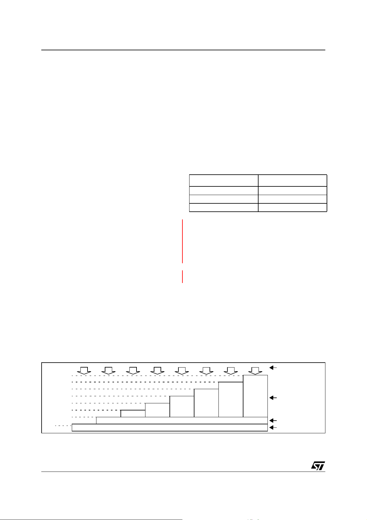
Depending on the overall Flash memory size in the
microcontroller device, there are up to three user
sectors (see Table 3). Each of these sectors can
be erased independently to avoid unnecessary
erasing of the whole Flas h memory when only a
partial erasing is required.
The first two sectors have a fixed siz e of 4 K bytes
(see Figure 6). They are mapped in the upper part
of the ST7 addressing space so the reset and interrupt vectors are located in Sector 0 (F000hFFFFh).
Table 3. Sectors available in Flash devices
Flash Size (bytes) Available Sectors
4K Sector 0
8K Sectors 0,1
> 8K Sectors 0,1, 2
4.3.1 Read-out Protection
Read-out protection, when selected, provides a
protection against Program Memory content extraction and against write access to Flash memory.
In Flash devices, this protection is removed by reprogramming the option. In this case, the entire
program memory is first automatically erased and
the device can be reprogrammed.
Read-out protection selection depends on the device type:
– In Flash devices it is enabled and removed
through the FMP_R bit in the option byte.
– In ROM devices it is enabled by mask option
specified in the Option List.
The Flash memory is organised in sectors and can
be used for both code and data storage.
Figure 6. Me m ory Map and Sec t or Address
4K 10K 24K 48K
1000h
3FFFh
7FFFh
9FFFh
BFFFh
D7FFh
DFFFh
EFFFh
FFFFh
16/262
8K 16K 32K 60K
2Kbytes
8Kbytes 40 Kbytes
16 Kbytes
4 Kbytes
4 Kbytes
24 Kbytes
FLASH
MEMORY SIZE
SECTOR 2
52 Kbytes
SECTOR 1
SECTOR 0
Page 17
FLASH PROGRAM MEMORY (Cont’d)
ST72561
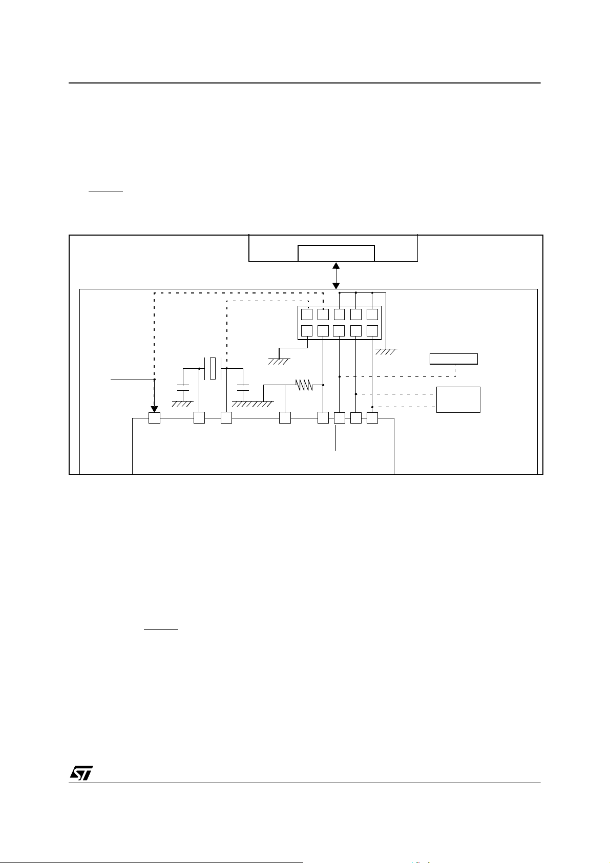
4.4 ICC Interface
ICC needs a minimum of 4 and up to 6 pins to be
connected to the programming tool (see Figure 7).
These pins are:
– RESET
– V
: device reset
: device power supply ground
SS
Figure 7. Typical ICC Interface
PROGRAMMING TOOL
APPLICATION
POWER SUPPLY
(See Note 3)
C
L2
DD
V
OSC2
OPTIONAL
(See Note 4)
C
L1
OSC1
ST7
Notes:
1. If the ICCCLK or ICCDATA pins are only used
as outputs in the application, no signal i solat ion is
necessary. As soon as the Programming Tool is
plugged to the board, even if an ICC session is not
in progress, the ICCCLK and ICCDATA pins are
not available for the application. If they are used as
inputs by the application, isolation such as a serial
resistor has to implemented i n case another device forces the signal. Refer to the Programming
Tool documentation for recommended resistor values.
2. During the ICC session, the programming tool
must control the RESET
flicts between the programming tool and the application reset circuit if it drives more than 5mA at
high level (push pull output or pull-up resistor<1K).
A schottky diode can be used to isolate th e application RESET circuit in this case. When using a
classical RC network with R>1K or a reset man-
pin. This can lead to con-
– ICCCLK: ICC output serial clock pin
– ICCDATA: ICC input/output serial data pin
– ICCSEL/V
: programming voltage
PP
– OSC1(or OSCIN): main clock input for exter-
nal source (optional)
– V
: application board power supply (opt ion-
DD
al, see Figure 7, Note 3)
ICC CONNECTOR
975 3
10kΩ
SS
V
ICCSEL/VPP
ICC Cabl e
RESET
ICCCLK
HE10 CONNECTOR TYPE
1
246810
ICCDATA
APPLICATION BOARD
ICC CONNECTOR
APPLICATION
RESET SOURCE
See Note 2
See Note 1
APPLICATION
I/O
agement IC with open drain outpu t and pull-up resistor>1K, no additional com ponents are needed.
In all cases the user must ensure that no external
reset is generated by the application during the
ICC session.
3. The use of Pin 7 of the ICC con nector de pends
on the Programming Tool architecture. This pin
must be connected when using most ST Programming Tools (it is used to monitor the application
power supply). Please refer to the Programming
Tool manual.
4. Pin 9 has to be connecte d to the OSC1 or OS CIN pin of the ST7 when the clock is not available
in the application or if the selec ted clock option is
not programmed in the opt ion byte. ST7 devices
with multi-oscillator capability need to hav e OS C2
grounded in this case.
17/262
Page 18

ST72561
FLASH PROGRAM MEMORY (Cont’d)
4.5 ICP (In-Circuit Programming)
To perform ICP the microcontroller must be
switched to ICC (In-Circuit Communication) mode
by an external controller or programming tool.
Depending on the ICP code dow nloaded in RAM,
Flash memory programming can be fully customized (number of bytes to prog ram, program locations, or selection serial communication interface
for downloading).
When using an STMicroelect ronics or third-party
programming tool that supp orts ICP and the s pecific microcontroller device, the user needs only to
implement the ICP hardware interface on the application board (see Figure 7). For more details on
the pin locations, refer to the device pinout description.
4.6 IAP (In-Applic ation Progra m m i ng)
This mode uses a BootLoader program previously
stored in Sector 0 by the user (in ICP mode or by
plugging the device in a programming tool).
This mode is fully controlled by user software. This
allows it to be adapted to the user application, (user-defined strategy for entering programming
mode, choice of communications protocol used to
fetch the data to be stored, etc.). For example, it is
possible to download code from the SPI, SCI, USB
or CAN interface and program it in the Flash. IAP
mode can be used to program any of the Flash
sectors except Sector 0, which is write/erase protected to allow recovery in case errors occur during the programming operation.
4.7 Related Documentation
For details on Flash program ming and I CC protocol, refer to the ST7 Flash Programming Reference Manual and to th e ST7 ICC Protocol Reference Manual
.
4.8 Register Description
FLASH CONTROL/STATUS REGISTER (FCSR)
Read/Write
Reset Value: 0000 0000 (00h)
70
00000000
This register is reserved for use by Programming
Tool software. It controls the Flash programming
and erasing operations.
Table 4. Flash Control/Status Register Address and Reset Value
Address
(Hex.)
0024h
18/262
Register
Label
FCSR
Reset Value00000000
76543210
Page 19

5 CENTRAL PRO CESSING UNI T
ST72561
5.1 INTRODUCTION
This CPU has a full 8-bit architecture and contains
six internal registers allowing efficient 8-bit data
manipulation.
5.2 MAIN FEATURES
■ Enable executing 63 basic instructions
■ Fast 8-bit by 8-bit multiply
■ 17 main addressing modes (with indirect
addressing mode)
■ Two 8-bit index registers
■ 16-bit stack pointer
■ Low power HALT and WAIT modes
■ Priority maskable hardware interrupts
■ Non-maskable software/hardware interrupts
Figure 8. CPU Registers
5.3 CPU REGISTERS
The 6 CPU registers shown in Figure 8 are not
present in the memory mapping and are accessed
by specific instruc tions.
Accumulator (A)
The Accumulator is an 8-bit general purpose register used to hold operan ds and the results of the
arithmetic and logic calculations and to manipulate
data.
Index Registers (X and Y)
These 8-bit registers are use d to create effective
addresses or as tempo rary storage areas f or data
manipulation. (The Cross-A ssembler generates a
precede instruction (PRE) to indicate that the following instruction refers to the Y register.)
The Y register is not affected by the interrupt automatic procedures.
Program Cou nt er (P C )
The program counter is a 16-bit register containing
the address of the next instruction to be executed
by the CPU. It is made of two 8-bit registers PCL
(Program Counter Low which is the LSB) and PCH
(Program Counter High which is the MSB).
70
RESET VALUE = XXh
70
RESET VALUE = XXh
70
RESET VALUE = XXh
15 8
RESET VALUE = RESET VECTOR @ FFFEh-FFFFh
15
RESET VALUE = STACK HIGHER ADDRESS
PCH
RESET VALUE =
7
70
1C1I1HI0NZ
1X11X1XX
70
8
PCL
0
ACCUMULATOR
X INDEX REGISTER
Y INDEX REGISTER
PROGRAM COUNTER
CONDITION CODE REGISTER
STACK POINTER
X = Undefined Value
19/262
Page 20
ST72561
CENTRAL PROCESSING UNIT (Cont’d)
Condition Code Register (CC)
Read/Write
Reset Value: 111x1xxx
70
11I1HI0NZ
C
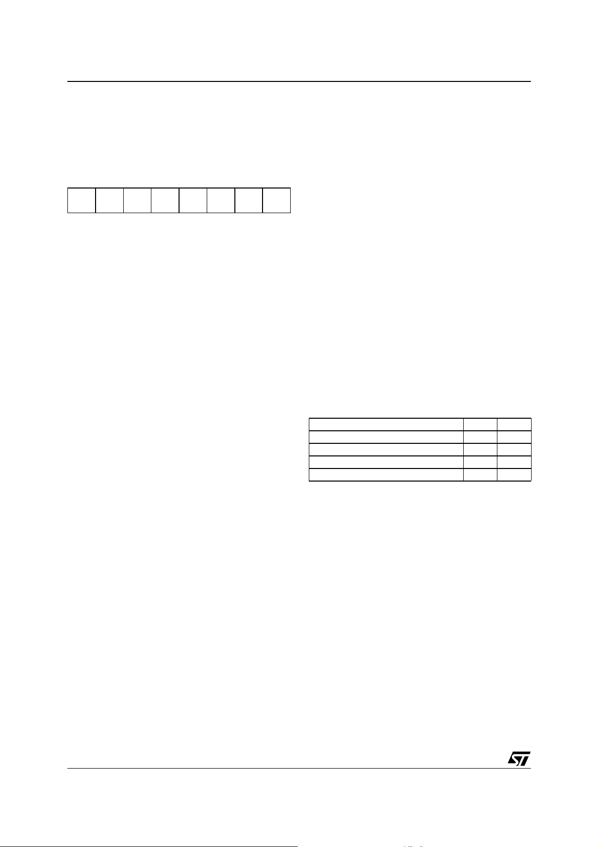
The 8-bit Condition Code register c ontains the interrupt masks and four flags representative of the
result of the instruction just executed. This register
can also be handled by the PUSH and POP instructions.
These bits can be individually tested and/or controlled by specific instructions.
Arithmetic Management Bits
Bit 4 = H Hal f carry.
This bit is set by hardware when a carry occurs be-
tween bits 3 and 4 of the A LU during an ADD or
ADC instructions. It is reset by hardware during
the same instruction s.
0: No half carry has occurred.
1: A half carry has occurred.
This bit is tested using the JRH or JRNH instruction. The H bit is useful in BCD arithmetic subroutines.
Bit 2 = N Negative.
This bit is set and cleared by hardware. It is repre-
sentative of the result sign of the last arithmetic,
logical or data manipulation. It’s a copy of the re-
th
sult 7
bit.
0: The result of the last operation is positive or null.
1: The result of the last operation is negative
(i.e. the most significant bit is a logic 1).
This bit is accesse d by the JRMI and JRPL instructions.
Bit 1 = Z Zero.
This bit is set and cleared by hardware. This bit in-
dicates that the result of the last arithmetic, logical
or data manipulation is zero.
0: The result of the last operation is different from
zero.
1: The result of the last operation is zero.
This bit is accessed by the JREQ and JRNE test
instructions.
Bit 0 = C Carry/borrow.
This bit is set and cleared b y hardware and software. It indicates an overflow or an underflow has
occurred during the last arithmetic operation.
0: No overflow or underflow has occurred.
1: An overflow or underflow has occurred.
This bit is driven by the SCF and RCF instructions
and tested by the JRC and JRNC instructions. It i s
also affected by the “bit test and branch”, shift and
rotate instructions.
Interrupt Managem ent B i ts
Bit 5,3 = I1, I0 Interrupt
The combination of the I1 and I0 bits gives the cur-
rent interrupt software priority.
Interrupt Software Priorit y I1 I0
Level 0 (main) 1 0
Level 1 0 1
Level 2 0 0
Level 3 (= interrupt disable) 1 1
These two bits are set/cleared b y hardware when
entering in interrupt. The loaded value is given by
the corresponding bits in the interrupt software priority registers (IxSPR). They can be also set/
cleared by software with the RIM, SIM, IRET,
HALT, WFI and PUSH/POP instructions.
See the interrupt management chapter for more
details.
20/262
Page 21
CENTRAL PROCESSING UNIT (Cont’d)
ST72561
Stack Pointer (SP)
Read/Write
Reset Value: 01 FFh
15 8
00000001
The least significant byte of the Stack Pointer
(called S) can be directly accessed by a LD instruction.
Note: When the lower limit is exceeded, the Stack
Pointer wraps around to the stack upper limit, without indicating the stack o verflow. The previously
stored information is then o verwritten and therefore lost. The stack also wraps in case of an underflow.
70
SP7 SP6 SP5 SP4 SP3 SP2 SP1
SP0
The stack is used to sav e the return address during a subroutine call and the CPU context during
an interrupt. The user may also directly manipulate
the stack by means of the PUSH and POP instruc-
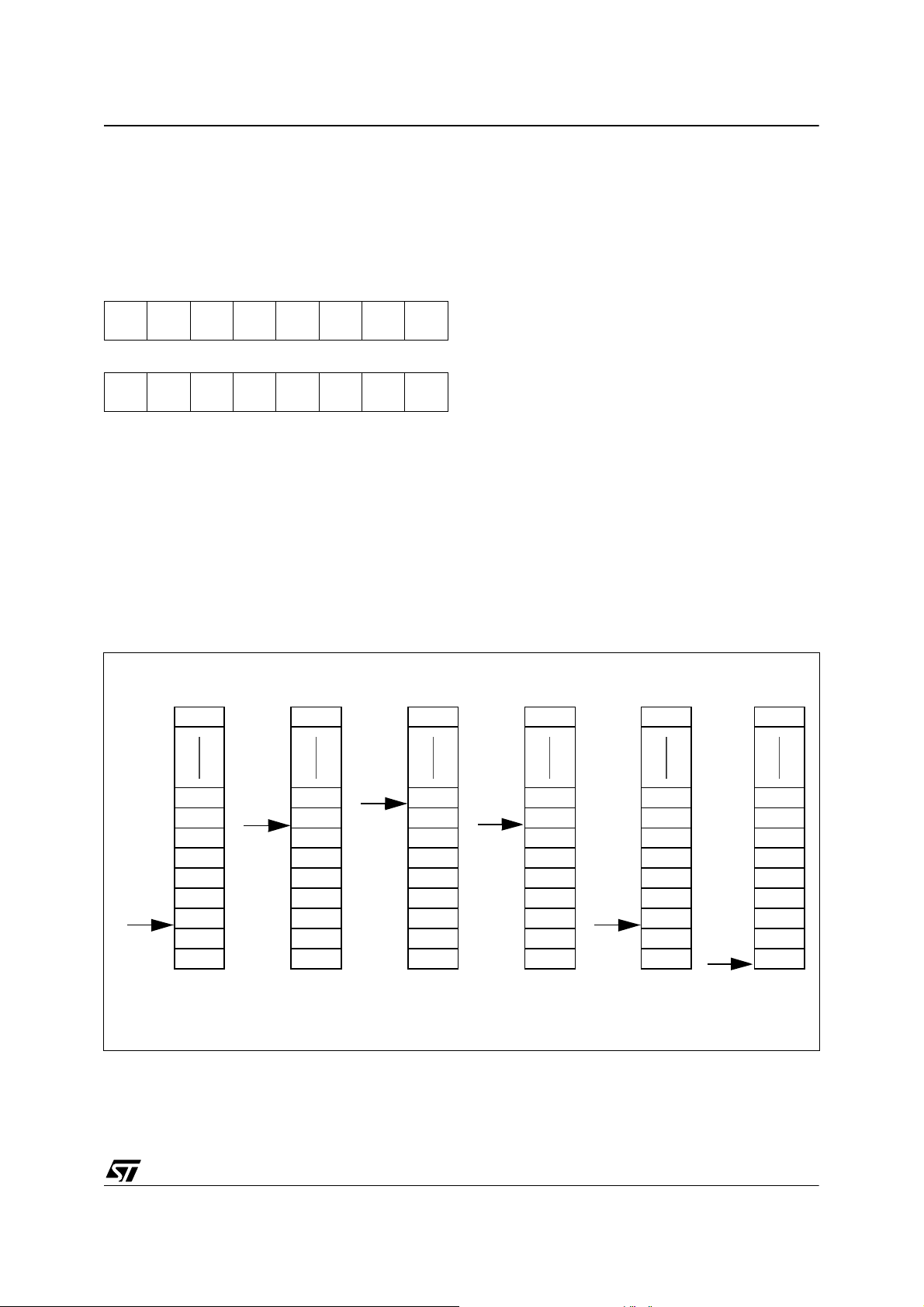
The Stack Pointer is a 16-bit register which is always pointing to the next free location in the stack.
It is then decremented after data has been pushed
onto the stack and incremented before data is
popped from the stack (see Figure 9).
Since the stack is 256 bytes deep, the 8 most significant bits are forced by hardw are. Following a n
MCU Reset, or after a Reset Stack Pointer i nstruction (RSP), the Stack Pointer contains its reset value (the SP7 to SP0 bits are set) which is the stack
tions. In the case of an interrupt, the PCL is stored
at the first location pointed t o by t he SP. Then the
other registers are stored in the next locations as
shown in Figure 9.
– When an interrupt is received, the SP is decre-
mented and the context is pushed on the stack.
– On return from interrupt, the SP is incremented
and the context is popped from the stack.
A subroutine call occupies two locations and an interrupt five locat ion s i n the sta ck ar ea.
higher address.
Figur e 9. Stack Manipulation Example
CALL
Subroutine
Interrupt
Event
PUSH Y POP Y IRET
RET
or RSP
@ 0100h
SP
@ 01FFh
SP
CC
A
X
PCH
PCL
PCH
PCL
Stack Higher Address = 01FFh
Stack Lower Address =
PCH
PCL
0100h
SP
Y
CC
A
X
PCH
PCL
PCH
PCL
SP
CC
A
X
PCH
PCL
PCH
PCL
SP
PCH
PCL
SP
21/262
Page 22
ST72561
6 SUPPLY, RESET AND CLOCK M ANAGEMENT
The device includes a range of utility features for
securing the application in critical situations (for
example in case of a power brown-out), and reducing the number of external components. An
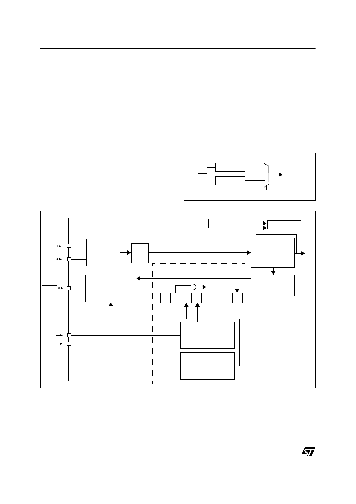
overview is shown in Figure 11.
For more details, refer to dedicated parametric
section.
Main features
■ Optional PLL for multiplying the frequency by 2
■ Reset Sequence Manager (RSM)
■ Multi-Oscillator Clock Management (MO)
– 4 Crystal/Ceram ic reso n ator oscilla t or s
■ System Integrity Management (SI)
– Main supply Low voltage detection (LVD)
– Auxiliary Voltage detector (AVD) with interrupt
capability for monitoring the main supply
Figure 11. Clock, Reset and Supply Block Diagram
OSC2
OSC1
MULTI-
OSCILLATOR
(MO)
f
OSC
PLL
(option)
f
OSC2
SYSTEM INTEGRITY MANAGEMENT
6.1 PHASE LOCKED LOOP
If the clock frequency input to the PLL is in the
range 2 to 4 MHz, the PLL can be used to multiply
the frequency by two to obtain an f
OSC2
of 4 to 8
MHz. The PLL is enabled by option byte. If the PLL
is disabled, then f
OSC2 = fOSC
/2.
Caution: T he PLL is not recom mended for applications where timing accuracy is required. See
“PLL Characteristics” on page 231.
Figure 10. PLL Block Diagram
f
OSC
PLL x 2
/ 2
/ 8000
0
1
PLL OPTION BIT
8-BIT TIMER
MAIN CLOCK
CONTROLLER
WITH REALTIME
CLOCK (MCC/RT C)
f
OSC2
f
CPU
RESET
V
SS
V
DD
22/262
RESET SEQUENCE
MANAGER
(RSM)
SICSR
0
AVD Inter rupt Reques t
AVD AVD
IE
LVD
F
RF
LOW VOLTAGE
DETECTOR
(LVD)
AUXILIARY VOLTAGE
DETECTOR
(AVD)
0
00
WATCHDOG
TIMER (WDG)
WDG
RF
Page 23
6.2 MULTI-OSCILLATOR (MO)
ST72561
The main clock of the ST7 can be generated by
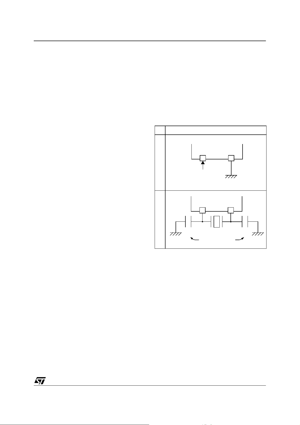
three different source types coming from the multioscillator block:
■ an external source
■ a crystal or ceramic resonator oscillator
Each oscillator is optimized for a given freq uency
range in terms of consumption and is selectable
through the option byte. The associated hardware
configuration are shown in Table 5. Refer to the
electrical characteristics section for more details.
Caution: T he OSC1 and/or OSC2 pins must not
be left unconnected. For the purpos es of Failure
Mode and Effect Analysis, it should be noted that if
the OSC1 and/or OSC2 pins are left unconnected,
the ST7 main oscillat or m ay s tart an d, in this c onfiguration, could generate an f
clock frequency
OSC
in excess of the allowed maximum (>16MHz.),
putting the ST7 in an unsafe/undefined state. The
product behaviour must therefore be considered
undefined when the OSC pins are left unc onnected.
External Clock Source
In external clock mode, a clock signal (square, sinus or triangle) with ~50% duty cycle has to driv e
the OSC1 pin while the OSC2 pin is tied to ground.
Crystal/Ceramic Oscillators
This family of oscillators has the advantage of producing a very accurate rate on the main clock of
the ST7. The selection within a list of 5 oscillators
with different frequency ran ges has to be done by
option byte in order to reduce consumption (refer
to Section 14.1 on p age 254 for more details on
the frequency ranges). The resonator and the load
capacitors have to be placed as close as possi ble
to the oscillator pins in order to minimize output
distortion and start-up stabilization time. The loading capacitance values must be adjusted according to the selected oscillator.
These oscillators are not stopped during the
RESET phase to avoid losing time in the oscillator
start-up phase.
Table 5. ST7 Clock Sources
Hardware Configuration
ST7
OSC1 OSC2
External ClockCrystal/Ceramic Resonators
EXTERNAL
SOURCE
OSC1 OSC2
C
L1
CAPACITORS
ST7
LOAD
C
L2
23/262
Page 24

ST72561
6.3 RESET SEQUENCE MANAGER (RSM)
6.3.1 Introd uc ti on
The reset sequence manager in cludes three RESET sources as shown in Figure 13:
■ External RESET source pulse
■ Internal LVD RESET (Low Voltage Detection)
■ Internal WATCHDOG RESET
These sources act on the RESET
pin and it is al-
ways kept low during the delay phase.
The RESET service routine vector is fixed at ad-
dresses FFFEh-FFFFh in the ST7 memory map.
The basic RESET sequence consists o f 3 p has es
as shown in F igure 12:
■ Active Phase depending on the RESET source
■ 256 or 4096 CPU clock cycle delay (selected by
opti on by te)
■ RESET vector fetch
The 256 or 4096 CPU clock cycle delay allows the
oscillator to stabilise and ensures that recovery
has taken place from the Reset st ate. T he short er
or longer clock cycle delay should be selected by
option byte to correspond to the stabilizat ion time
of the external oscillator used in the application.
Figure 13. Reset Block Diagram
The RESET vector fetch phase duration is 2 clock
cycles.
Figure 12. RESET Sequence Phases
RESET
Active Phase
INTERNAL RE SE T
256 or 4096 CLOCK CYCLES
6.3.2 Asynchr onous Externa l RESET
The RESET
output with integrated R
pin is both an input and an open-drain
weak pull-up resistor.
ON
FETCH
VECTOR
pin
This pull-up has no f ixed value but varies in accordance with the input voltage. It
can be pulled
low by external circuitry to reset the device. See
Electrical Characteristic section for more details.
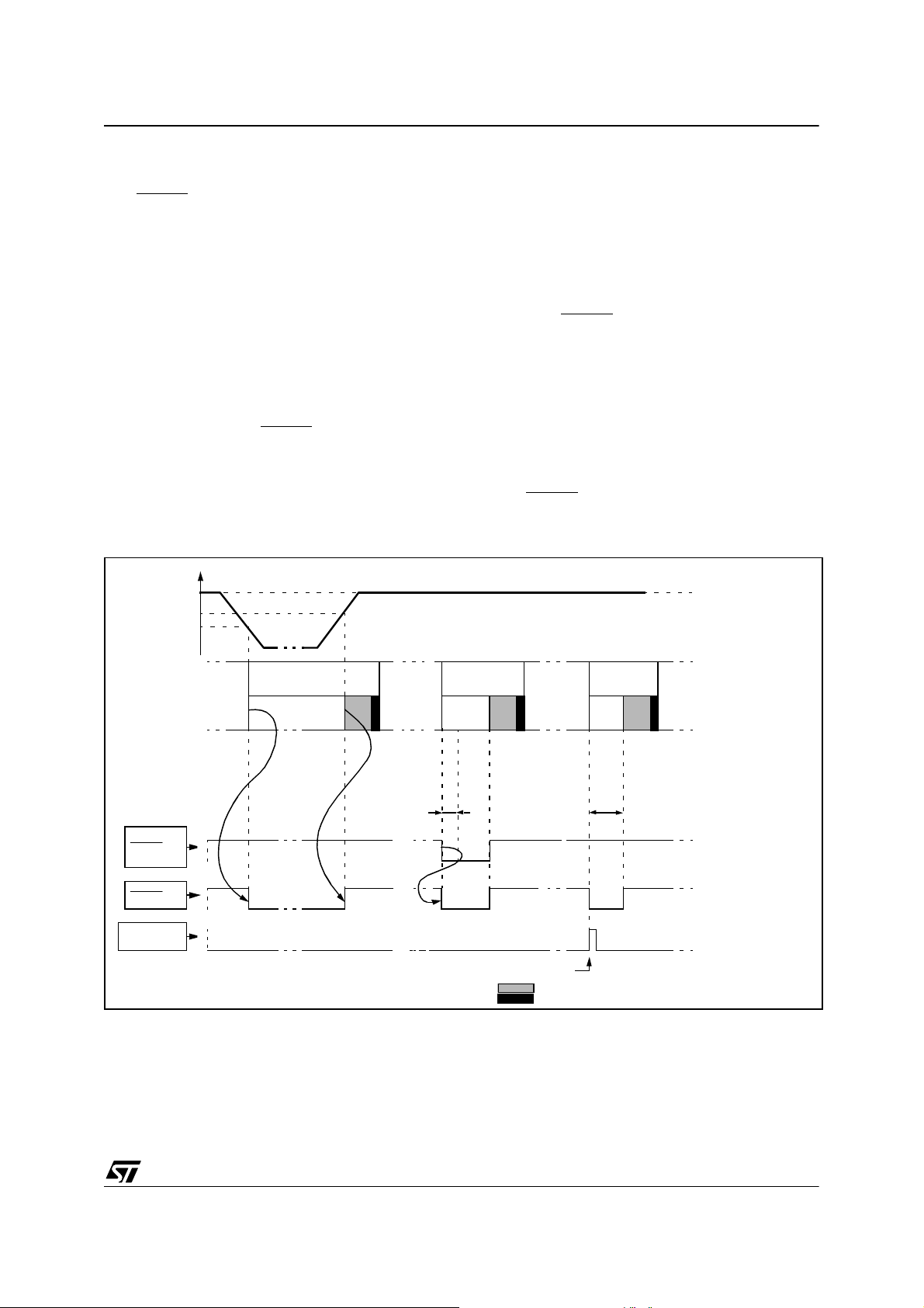
A RESET signal originating from an external
source must have a duration of at least t
h(RSTL)in
in
order to be recognized (see Figure 14). This detection is asynchronous and therefore the MCU
can enter reset state even in HALT mode.
RESET
V
DD
R
ON
Filter
PULSE
GENERATOR
INTERNAL
RESET
WATCHDOG RESET
LVD RESET
24/262
Page 25
RESET SEQUENCE MANAGER (Cont’d)
The RESET
pin is an asynchronous signal which
plays a major role in EMS performance. In a noisy
environment, it is recommended to follow the
guidelines mentioned in the electrical charact eristics section.
6.3.3 External Power-On RESET
If the LVD is disabled by option byte, to s tart up the
microcontroller correctly, the user must ensure by
means of an external reset circuit that the reset
signal is held low until V
level specified for the selected f
A proper reset signal for a slow rising V
is over the m inimum
DD
frequency.
OSC
supply
DD
can generally be provided by an ext ernal RC network connected to the RESET
pin.
Figure 14. RESET Sequences
V
DD
ST72561
6.3.4 Internal Low Voltage Detector (LVD)
RESET
Two differen t RESET sequences caused by the internal LVD circuitry can be distinguished:
■ Power-On RESET
■ Voltage Drop RESET
The device RESET
pulled low when V
V
DD<VIT-
(falling edge) as shown in Figure 14.
The LVD filters spikes on V
avoid parasitic resets.
6.3.5 Internal Watchdog RESET
The RESET sequence generated by a internal
Watchdog counter overflow is shown in Figure 14.
Starting from the Watchdog counter underflow, the
device RESET
low during at least t
pin acts as an output that is
DD<VIT+
(rising edge) or
larger than t
DD
g(VDD)
to
pin acts as an output that is pulled
w(RSTL)out
.
V
IT+(LVD)
V
IT-(LVD)
EXTERNAL
RESET
SOURCE
RESET PIN
WATCHDOG
RESET
RUN
LVD
RESET
ACTIVE PHASE
RUN
t
h(RSTL)in
EXTERNAL
RESET
ACTIVE
PHASE
WATCHDOG UNDERFLOW
RUN RUN
INTERNAL RESET (256 or 4096 T
VECTOR FETCH
WATCHDOG
RESET
ACTIVE
PHASE
t
w(RSTL)out
CPU
)
25/262
Page 26

ST72561
6.4 SYSTEM INTEGRITY MANAGEMENT (SI)
The System Integrity Mana gement b lock contains
the Low Voltage Detector (LVD) and Auxiliary Voltage Detector (AVD) functions. It is managed by
the SICSR register.
6.4.1 Low Voltage Detector (LVD)
The Low Voltage Detector funct ion (LVD) generates a static reset when the V
below a V
IT-(LVD)
reference value. This means that
supply voltage is
DD
it secures the power-up as well as the power-down
keeping the ST7 in reset.
The V
IT-(LVD)
lower than the V
on in order to avoid a parasitic reset when the
reference value for a voltage drop is
IT+(LVD)
reference value for power-
MCU starts running and sinks current on the supply (hysteresis).
The LVD Reset circuitry generates a res et when
is below:
V
DD
– V
– V
IT+(LVD)
IT-(LVD)
when VDD is rising
when VDD is falling
The LVD func t io n is illustrate d in F igure 15.
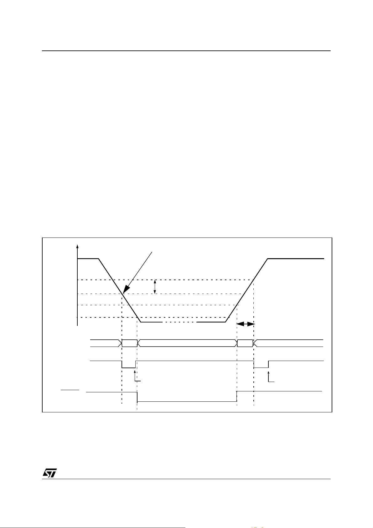
Figure 15. Low Voltage Detector vs Reset
V
DD
Provided the minimum V
the oscillator frequency) is above V
MCU can only be in two modes:
value (guaranteed for
DD
IT-(LVD)
, the
– under full software control
– in static safe reset
In these conditions, secure operation is always ensured for the application without the need for external reset hardware.
During a Low Voltage Detector Reset, the RESET
pin is held low, thus p ermitting the MCU to reset
other devices.
Notes:
The LVD allows the device to be used without any
external RESET circuitry.
The LVD is an optional func tion which can be se-
lected by option byte.
It is recommended to make sure that the V
DD
supply voltage rises monotonously when the device is
exiting from Reset, to ensure the application functions properly.
V
IT+
(LVD)
V
IT-
(LVD)
RESET
V
hys
26/262
Page 27
SYSTEM INTEGRITY MANAGEMENT (Cont’d)
6.4.2 Auxiliary Voltage Detector (AVD)
The Voltage Detector function (AVD) i s based on
an analog comparison between a V
V
IT+(AVD)
ply. The V
age is lower than the V
reference value and the VDD main sup-
IT-(AVD)
reference value for falling volt-
IT+(AVD)
reference value for
IT-(AVD)
and
rising voltage in order to avoid parasitic detection
(hysteresis).
The output of the AVD comparator is directly readable by the application software through a real
time status bit (AVDF) in t he SI CS R regi ster. This
bit is read only.
Caution: The AVD function is active only if the
LVD is enabled through the option byte.
6.4.2.1 Monitoring the V
Main Su pply
DD
If the AVD interrupt is enabled, an interrupt is generated when the voltage crosses the V
V
IT-(AVD)
threshold (AVDF bit toggles).
IT+(AVD)
or
In the case of a drop in v oltage, th e A VD interrupt
acts as an early warning, allowing software to shut
ST72561
down safely before the LVD re sets the microcontroller. See Figure 16.
The interrupt on the rising edge is used to inform
the application that the V
If the voltage rise time t
CPU cycles (depending on the reset delay selected by option byte), no AVD interrupt will be generated when V
If t
is greater than 256 or 4096 cycles then:
rv
IT+(AVD)
is reached.
– If the AVD interrupt is enabled before the
V
IT+(AVD)
threshold is reached, then 2 AVD interrupts will be received: the first when the AVDIE
bit is set, and the second when the threshold is
reached.
– If the AVD interrupt is enabled after the V
threshold is reached then only one AVD interrupt
will occur.
warning state is over.
DD
is less than 256 or 4096
rv
IT+(AVD)
Figure 16. Using the AVD to Monitor V
V
DD
DD
Early Warning Interr upt
(Power has dropped, MCU not
not yet in reset)
V
V
IT+(AVD)
V
IT-(AVD)
V
IT+(LVD)
V
IT-(LVD)
AVDF bit 0 0RESET VALUE
AVD INTERRUPT
REQUEST
IF AVDIE bit = 1
LVD RESET
1
hyst
INTERRUPT PROCESS
t
VOLTAGE RISE TIME
rv
1
INTERRUPT PROCESS
27/262
Page 28

ST72561
SYSTEM INTEGRITY MANAGEMENT (Cont’d)
6.4.3 Low Power Modes
Mode Description
WAIT
HALT The SICSR register is frozen.
6.4.3.1 Interrupts
The AVD interrupt event generates an interrupt if
the AVDIE bit is set and the interrupt mask in the
CC register is reset (RIM instructio n ).
No effect on SI. AVD interrupts cause the
device to exit from Wait mode.
Flag
Enable
Control
Bit
Interrupt Event
AVD event AVDF AVDIE Yes No
Event
Exit
from
Wait
Exit
from
Halt
28/262
Page 29

SYSTEM INTEGRITY MANAGEMENT (Cont’d)
6.4.4 Register Description
SYSTEM INTEGRITY (SI) CONTROL/STATUS REGISTER (SICSR)
Read/Write
Reset Value: 000x 000x (00h)
Bits 3:1 = Reserved, must be kept cleared.
ST72561
70
AVD
IE
AVDFLVD
RF
000
0
WDG
RF
Bit 0 = WDGRF Watchdog reset flag
This bit indicates that the last Reset was generated by the Watchdog p eripheral. It is set by hardware (watchdog reset) and cleared by software
Bit 7 = Reserved, must be kept cleared.
(writing zero) or an LVD Reset (to ensure a stable
cleared state of the WDGRF flag when CPU
starts).
Bit 6 = AVDIE Voltage Detector interrupt enable
This bit is set and cleared by software. It enables
an interrupt to be generated when the AVDF flag
changes (toggles). The pending interrupt information is automatically cleared when software enters
the AVD interrupt routine.
0: AVD interrupt disabled
Combined with the LVDRF flag information, the
flag description is given by the following table.
RESET Sources LVDRF WDGRF
External RESET
Watchdog 0 1
LVD 1 X
pin 0 0
1: AVD interrupt enabled
Bit 5 = AVDF Voltage Detector flag
This read-only bit is set and cleared by hardware.
If the AVDIE bit is set, an interrupt request is generated when the AVDF bit changes value. Refer to
Figure 16 and to Section 6. 4.2.1 for additional de-
tails.
0: V
1: V
over V
DD
under V
DD
IT+(AVD)
IT-(AVD)
threshold
threshold
Application note s
The LVDRF flag is not cleared when another RESET type occurs (external or watchdog), the
LVDRF flag remains set to keep tra ce of the original failure.
In this case, a watchdog reset can be detected by
software while an external reset can not.
CAUTION: When the LVD is not activated with the
associated option byte, the WDGRF flag can not
Bit 4 = L VDRF LVD reset flag
be used in the application.
This bit indicates that the last Reset was generated by the LVD block. It is set by hardware (LVD reset) and cleared by software (writing zero). See
WDGRF flag description for more details. When
the LVD is disabled by OPTION BYTE, the LVDRF
bit value is undefined.
29/262
Page 30

ST72561
7 INTERRUPTS
7.1 INTRODUCTION
The ST7 enhanced interrupt management provides the following features:
■ Hardware interrupts
■ Software interrupt (TRAP)
■ Nested or concurrent interrupt management
with flexible interrupt priority and level
management:
– Up to 4 software programmable nesting levels
– Up to 16 interrupt vectors fixed by hardware
– 2 non maskable events: RESET, TRAP
– 1 maskable Top Level Event: TLI
This interrupt management is based on:
– Bit 5 and bit 3 of the CPU CC register (I1:0),
– Interrupt software priority registers (ISPRx),
– Fixed interrupt vector addresses located at the
high addresses of the memory map (FFE0h to
FFFFh) sorted by hardware priority order.
This enhanced interrupt cont roller guarantees full
upward compatibility with the standard (not nested) ST7 interrupt controller.
7.2 MASKIN G AN D PROC ESSING FLOW
The interrupt masking is managed by the I1 and I0
bits of the CC register and the ISPRx registers
which give the interrupt software priority level of
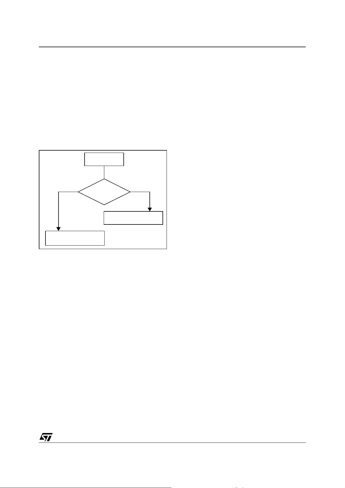
each interrupt vector (see Table 6). The processing flow is shown in Figure 17
When an interrupt request has to be serviced:
– Normal processing is suspended at the end of
the current instruction execution.
– The PC, X, A and CC registers are saved onto
the stack.
– I1 and I0 bits of CC register are set according to
the corresponding values in the ISPRx registers
of the serviced interrupt vector.
– The PC is then loaded with the interrupt vector of
the interrupt to service and the first instruction of
the interrupt service routine is fetched (refer to
“Inter rupt M a pping ” table for vector addresses).
The interrupt service routine should end with the
IRET instruction which causes the contents of the
saved registers to be recovered from the stack.
Note: As a consequence of the IRET instruction,
the I1 and I0 bits will be rest ored from the stack
and the program in the previous level will resume.
Table 6. Interrupt Software Priority Levels
Interrupt software priority Level I1 I0
Level 0 (main) Low
Level 1 0 1
Level 2 0 0
Level 3 (= interrupt disable) 1 1
High
10
Figure 17. Int errupt Proces s in g Fl owchart
RESET
RESTORE PC, X, A, CC
FROM STACK
30/262
PENDING
INTERRUPT
N
FETCH NEX T
INSTRUCTION
Y
“IRET”
N
EXECUTE
INSTRUCTION
Y
THE INTERRUPT
STAYS PENDING
TLI
Interrupt has th e sam e or a
lower software priority
than current on e
STACK PC, X, A, CC
LOA D I1:0 FROM IN TERRUPT SW REG.
LOAD PC FROM INTERRUPT VECTOR
N
I1:0
software priority
than current one
Interrupt has a higher
Y
Page 31
INTERRUPTS (Cont’d)
ST72561
Servicing Pending Inte rrupts
As several interrupts can b e pending at the sam e
time, the interrupt to be taken into account is determined by the following two-step process:
– the highest software priority interrupt is serviced,
– if several interrupts have the same software pri-
ority then the interrupt with the highest hardware
priority is serviced first.
Figure 18 describes this decision process.
Figure 18. Priority Decision Process
PENDING
INTERRUPTS
Same
HIGHEST HARDWARE
PRIORITY SERVICED
SOFTWARE
PRIORITY
HIGHEST SOFTWARE
PRIORITY SERVICED
Different
When an interrupt request is not serviced immediately, it is latched and then processed when its
software priority combined with the hardware priority becomes the highest one.
Note 1: The hardware priority is exclusive while
the software one i s not. This allows the previ ous
process to succeed with only one interrupt.
Note 2: RESET, TRAP and TLI can be considered
as having the highest software priority in the decision process.
Different Interrupt Vector Sources
Two interrupt source types are managed by the
ST7 interrupt controller: the non-maskable type
(RESET, TRAP) and the maskable type (ex ternal
or from internal peripherals).
Non-Maskable Sources
These sources are processed regardless of the
state of the I1 a nd I0 bits of the CC register (see
Figure 17). After stacking the PC, X, A and CC
registers (except for RESET), the corresponding
vector is loaded in the PC re gister and the I1 an d
I0 bits of the CC are set to disable interrupts (level
3). These sources allow the processor to exit
HALT mode.
■ TRAP (Non Maskable Software Interrupt)
This software interrupt is serviced when the TRAP
instruction is executed. It will be serviced according to the flowchart in Figure 17 as a TLI.
Caution: TRAP can be interrupted by a TLI.
■ RESET
The RESET source has the highest priority in the
ST7. This means that the first current routine has
the highest software priority (level 3) and the highest hardware priority.
See the RESET chapter for more details.
Maskable Sources
Maskable interrupt ve ctor sourc es can be servi ced
if the corresponding interrupt is e nabled and if its
own interrupt software priority (in ISPRx registers)
is higher than the one currently being serviced (I1
and I0 in CC register). If any of these two conditions is false, the interrupt is latched and thus remains pending.
■ TLI (Top Level Hardware Interrupt)
This hardware interrupt occurs when a specific
edge is detected on the dedicated TLI pin.
Caution: A TRAP instruction must not be used in a
TLI service routine.
■ External Interrupts
External interrupts allow the processor to exit from
HALT low power mode.
External interrup t s en s it iv ity is so ft w ar e selectab le
through the External Interrupt Control register
(EICR).
External interrupt triggered on edge will be latched
and the interrupt request automatically cleared
upon entering the interrupt service routine.
If several input pins of a grou p connected to the
same interrupt line are selected simultaneously,
these will b e lo gically OR ed .
■ Peripheral Interrupts
Usually the peripheral interrupts cause the MCU to
exit from HALT m ode except those mentioned in
the “Interrupt Mapping” table.
A peripheral interrupt occurs when a specific flag
is set in the peripheral status registers and if the
corresponding enable bit is set in the peripheral
control register.
The general sequence for clearing an interrupt is
based on an access to the status register followed
by a read or write to an associated register.
Note: The clearing sequence resets the internal
latch. A pending interrupt (i.e. waiting for being
serviced) will therefore be lost if the clear sequence is executed.
31/262
Page 32
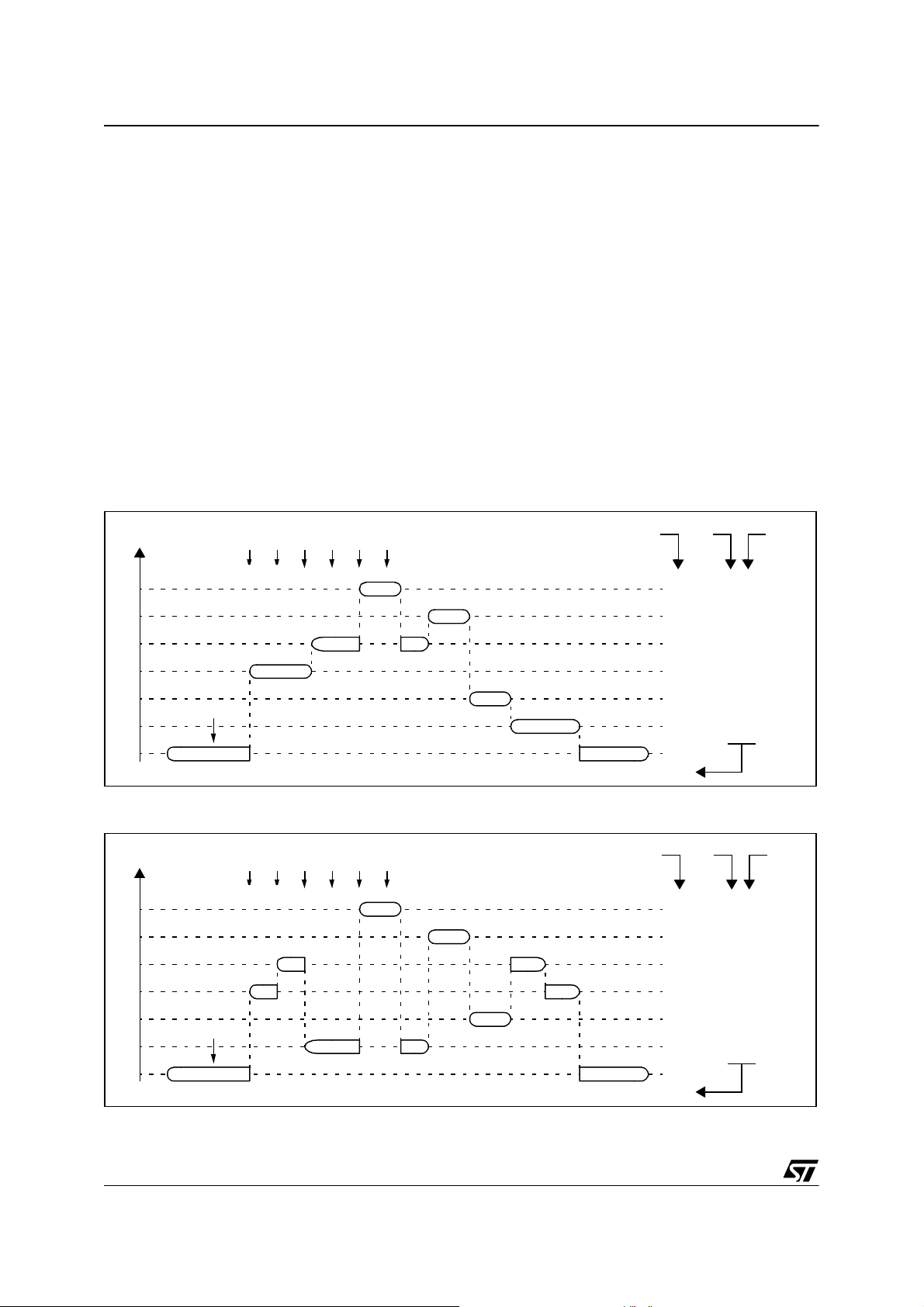
ST72561
INTERRUPTS (Cont’d)
7.3 INTERRUPTS AND LOW POWER MODES
All interrupts allow the processor to exit the WAIT
low power mode. On the contrary, only external
and other specified interrupt s allow the processor
to exit from the HALT modes (see column “Exit
from HALT” in “Interrupt Mapping” table). When
several pending interrupts are present whi le exiting HALT mode, the first one serviced can only be
an interrupt with e xit from HALT mo de capability
and it is selected through the same decision process shown in Figure 18.
Note: If an interrupt, that is not able to Exit from
HALT mode, is pending with the highest priority
when exiting HALT mode, this interrupt is serviced
after the first one serviced.
Figure 19. Con c u rre n t Int errupt Management
IT1
TLI
IT3
IT0
TLI
IT1
RIM
IT2
IT1
IT4
IT2
HARDWARE PRIORITY
MAIN
11 / 10
7.4 CONCURRENT & NESTED MANAGEMENT
The following Figure 19 and Figure 20 show two
different interrupt management modes. The first is
called concurrent mode and do es not allow an interrupt to be interrupted, unlike the nested mode in
Figure 20. The interrupt hardware priority is given
in this order from the l owest to the hi ghes t: MA IN,
IT4, IT3, IT2, IT1, IT 0, TLI. The so ftwa r e pr io rity is
given for each interrupt.
Warning: A stack overflow may occur without notifying the software of the failure.
SOFTWARE
PRIORITY
LEVEL
IT0
IT3
IT4
MAIN
3
3
3
3
3
3
3/0
I1
11
11
11
11
11
11
10
I0
USED STACK = 10 BYTES
Figure 20. Nested Interrupt Management
IT2
IT1
IT4
IT1
IT2
RIM
HARDWARE PRIORITY
MAIN
TLI
IT3
IT4 IT4
IT0
TLI
11 / 10
32/262
IT0
IT3
IT1
SOFTWARE
PRIORITY
LEVEL
IT2
10
MAIN
I1 I0
3
3
2
1
3
3
3/0
11
11
00
01
11
11
USED STACK = 20 BYTES
Page 33
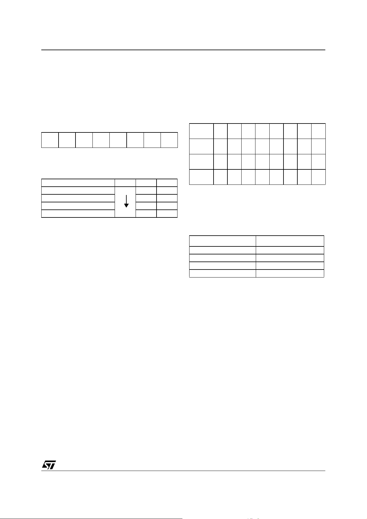
INTERRUPTS (Cont’d)
ST72561
7.5 INTERRUPT REGISTER DESCRIPTION
INTERRUPT SOFTWARE PRIORITY REGISTERS (ISPRX)
CPU CC REGISTER INTERRUPT BITS
Read/Write
Reset Value: 111x 1010 (xAh)
70
11I1 H I0 NZC
Bit 5, 3 = I1, I0 Softwar e Interr u p t Priori ty
These two bits indicate the current interrupt soft-
ware priority.
Interrupt Software Priority Level I1 I0
Level 0 (main) Low
Level 1 0 1
Level 2 0 0
Level 3 (= interrupt disable*) 1 1
High
10
These two bits are set/cleared by hardware whe n
entering in interrupt. The loaded value is given by
the corresponding bits in the interrupt software priority registers (ISPRx).
They can be also set/cleared by sof t ware wi th th e
RIM, SIM, HALT, WFI, IRET and PUSH/POP instructions (see “Interrupt Dedicated Instruction
Set” table).
*Note: TLI, TRAP and RESET events ca n in terru pt
a level 3 program.
Read/Write (bit 7:4 of ISPR3 are read only)
Reset Value: 1111 1111 (FFh)
70
ISPR0 I1_3 I0_3 I1_2 I0_2 I1_1 I0_1 I1_0 I0_0
ISPR1 I1_7 I0_7 I1_6 I0_6 I1_5 I0_5 I1_4 I0_4
ISPR2 I1_11 I0_11 I1_10 I0_10 I1_9 I0_9 I1_8 I0_8
ISPR3 1 1 1 1 I1_13 I0_13 I1_12 I0_12
These four registers contain the interrupt software
priority of each interrupt vector.
– Each interrupt vecto r (except RESET and TRAP)
has corresponding bits in these registers where
its own software priority is stored. This correspondance is shown in the following table.
Vector address ISPRx bits
FFFBh-FFFAh I1_0 and I0_0 bits*
FFF9h-FFF8h I1_1 and I0_1 bits
... ...
FFE1h-FFE0h I1_13 and I0_13 bits
– Each I1_x and I0_x bit value in the ISPRx regis-
ters has the same meaning as the I1 and I0 bits
in the CC register.
– Level 0 can not be written (I1_x=1, I0_x=0). In
this case, the previously stored value is kept. (example: previous=CFh, write=64h, result=44h )
The RESET, TRAP and TLI v ectors have no sof tware priorities. When one is serviced, the I1 and I0
bits of the CC register are both set.
*Note: Bits in the ISPRx registers which correspond to the TLI can be read and written but they
are not significant in the interrupt process management.
Caution: If the I1_x and I0_x bits are modified
while the interrupt x is executed the following behaviour has to be considered: If the interrupt x is
still pending (new interrupt or flag not cleared) and
the new software priority is higher than the previous one, the interrupt x is re-entered. Otherwise,
the software priority stays unchanged up to the
next interrupt request (after the IRET of the interrupt x).
33/262
Page 34
ST72561
INTERRUPTS (Cont’d)
Table 7. Dedicated Interrupt Instruction Set
Instruction New Description Function/Example I1 H I0 N Z C
HALT Entering Halt mode 1 0
IRET Interrupt routine return Pop CC, A, X, PC I1 H I0 N Z C
JRM Jump if I1:0=11 (level 3) I1:0=11 ?
JRNM Jump if I1:0<>11 I1:0<>11 ?
POP CC Pop CC from the Stack Mem => CC I1 H I0 N Z C
RIM Enable interrupt (level 0 set) Load 10 in I1:0 of CC 1 0
SIM Disable interrupt (level 3 set) Load 11 in I1:0 of CC 1 1
TRAP Software trap Software NMI 1 1
WFI Wait for interrupt 1 0
Note: During the execution of an interrupt routine, the HALT, POPCC, RIM, SIM and WFI instructions change the current
software priority up to the next IRET instruction or one of the previously mentioned instructions.
34/262
Page 35
INTERRUPTS (Cont’d)
Table 8. Interrupt Mapping
ST72561
N°
Source
Block
Description
RESET Reset
TRAP Software interr upt no FFFCh-FFFDh
0 TLI External top level interrupt EICR yes FFFAh-FFFBh
Register
Label
N/A
Priority
Order
Highest
Priority
Exit
from
HALT
yes FFFEh-FFFFh
1)
Address
Vector
1 MCC/RTC Main clock controller time base interrupt MCCSR yes FFF8h-FFF9h
2 ei0/AWUFH External interrupt ei0/ Auto wake-up from Halt
3 ei1/AVD External interrupt ei1/Auxiliary Voltage Detector
EICR/
AWUCSR
EICR/
SICSR
yes
FFF6h-FFF7h
2)
FFF4h-FFF5h
4 ei2 External interrupt ei2 EICR FFF2h-FFF3h
5 ei3 External interrupt ei3 EICR FFF0h-FFF1h
6 CAN CAN peripheral interrupt - RX CIER no FFEEh-FFEFh
7 CAN CAN peripheral interrupt - TX / ER / SC CIER yes
3)
FFECh-FFEDh
8 SPI SPI peripheral interrupts SPICSR yes FFEAh-FFEBh
9 TIMER8 8-bit TIMER peripheral interrupts T8_TCR1 no FFE8h-FFE9h
10 TIMER16 16-bit TIMER peripheral interrupts TCR1 no FFE6h-FFE7h
11
12
LINSCI2 LINSCI2 Peripheral interru pts SCI2CR1 no FFE4h-FFE5h
LINSCI1
LINSCI1 Peripheral interru pts (LIN Master/
Slave)
SCI1CR1 no
Lowest
Priority
4)
FFE2h-FFE3h
13 PWM ART 8-bit PWM ART interrupts PWMCR yes FFE0h-FFE1h
Notes:
1. Valid for HALT and ACTIVE-HALT m odes excep t for the MCC/RTC interrupt source wh ich exits from
ACTIVE-HALT mode only.
2. Except AVD interrupt
3. Exit from Halt only when a wake-up condi tion is detected, generat ing a Sta tus Change inte rrupt. See
Section 10.9.5 on page 187.
4. It is possible to exit from Halt using the external interrupt which is mapped on the RDI pin.
35/262
Page 36
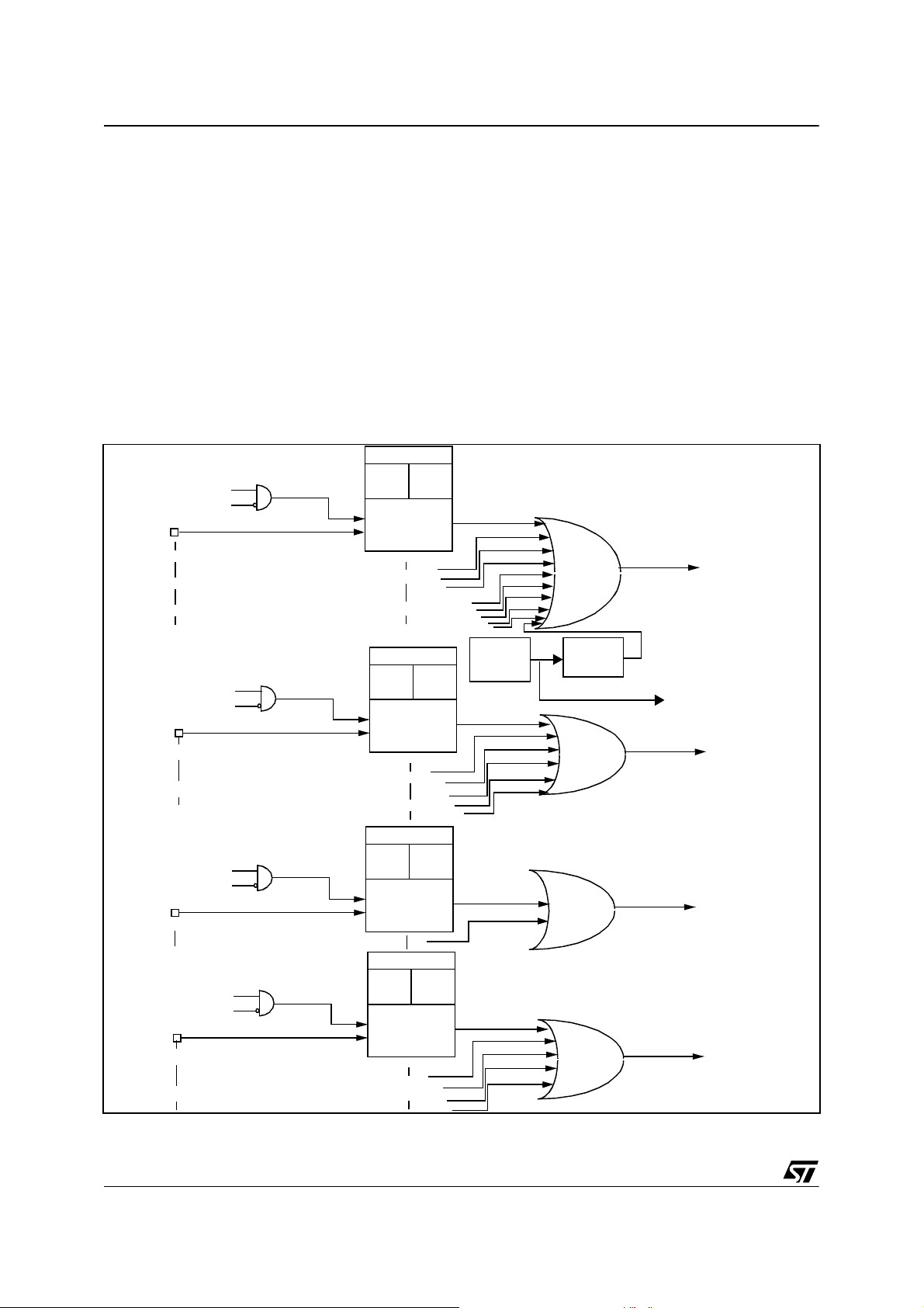
ST72561
INTERRUPTS (Cont’d)
7.6 EXTERNAL INTERRUPTS
7.6.1 I/O PORT INTERRUPT SENSITIVITY
The external interrupt sensitivity is controlled by
the ISxx bits in the EICR register (Figure 21). This
control allows up to 4 fully independent external interrupt source sensitivities.
Each external interrupt source can be generated
on four (or five) different events on the pin:
■ Falling edge
■ Rising edge
Figure 21. External Interrupt Control bits
PORT A [7:0] INTERRUPTS
PAOR.0
PADDR.0
PA0
PORT B [5:0] INTERRUPTS
PBOR.0
PBDDR.0
PB0
EICR
IS00 IS01
SENSITIVITY
CONTROL
EICR
IS10 IS11
SENSITIVITY
CONTROL
■ Falling and rising edge
■ Falling edge and low level
To guarantee correct functionality, the sensitivity
bits in the EICR register can be modified only
when the I1 and I0 bits of the CC register are both
set to 1 (level 3). This means that interrupts must
be disabled before changing sensitivity.
The pending interrupts are cleared by writing a different value in the ISx[1:0] of the EICR.
PA0
PA1
PA2
PA3
AWUFH
Oscillator
PB0
PB1
PB2
PB3
PB4
PB5
PA4
PA5
PA6
PA7
/ AWUPR
To Tim e r In put Capt ur e 1
ei0 INTERRUPT SOURCE
ei1 INTERRUPT SOURCE
36/262
PORT C [2:1] INT E RRUPTS
PCOR.7
PCDDR.7
PC1
PORT D [7:6, 4, 1:0] INTERR UPTS
PDOR.0
PDDDR.0
PD0
EICR
IS20 IS21
SENSITIVITY
CONTROL
EICR
IS30 IS31
SENSITIVITY
CONTROL
PC1
PC2
PD0
PD1
PD4
PD6
PD7
ei2 INTER RUPT SOURCE
ei3 INTERRUPT S O URCE
Page 37
INTERRUPTS (Cont’d)
7.6.2 Register Description
EXTERNAL INTERRUPT CONTROL
These 2 bits can be written only when I1 and I0 of
the CC register are both set to 1 (level 3).
REGISTER 0 (EICR0)
Read/Write
Reset Value: 0000 0000 (00h)
70
IS31 IS30 IS21 IS20 IS11 IS10 IS01 IS00
Bit 7:6 = IS3[1:0] ei3 sensitivity
The interrupt sensitivity, defined using the IS3[1:0]
bits, is applied to the ei3 external interrupts:
Bit 1:0 = IS0[1:0] ei0 sensitivity
The interrupt sensitivity, defined using the IS0[1:0]
bits, is applied to the ei0 external interrupts:
IS01 IS00 External Interrupt Sensitivity
0 0 Falling edge & low level
0 1 Rising edge only
1 0 Falling edge only
1 1 Rising and falling edge
ST72561
IS31 IS30 Exte rnal Interr upt Sensit ivity
0 0 Falling edge & low level
0 1 Rising edge only
1 0 Falling edge only
1 1 Rising and falling edge
These 2 bits can be written only when I1 and I0 of
the CC register are both set to 1 (level 3).
Bit 5:4 = IS2[1:0] ei2 sensitivity
The interrupt sensitivity, defined using the IS2[1:0]
bits, is applied to the ei2 external interrupts:
IS21 IS20 Exte rnal Interr upt Sensit ivity
0 0 Falling edge & low level
0 1 Rising edge only
1 0 Falling edge only
1 1 Rising and falling edge
These 2 bits can be written only when I1 and I0 of
the CC register are both set to 1 (level 3).
Bit 3:2 = IS1[1:0] ei1 sensitivity
The interrupt sensitivity, defined using the IS1[1:0]
bits, is applied to the ei1 external interrupts:
IS11 IS10 Exte rnal Interr upt Sensit ivity
0 0 Falling edge & low level
0 1 Rising edge only
1 0 Falling edge only
1 1 Rising and falling edge
These 2 bits can be written only when I1 and I0 of
the CC register are both set to 1 (level 3).
EXTERNAL INTERUPT CONTROL REGISTER 1
(EICR1)
Read/Write
Reset Value: 0000 0000 (00h)
70
000000TLISTLIE
BIt 7:2 = Reserved
Bit 1 = TLIS Top Level Interrupt sensitivity
This bit configures the TLI edge sensitivity. It can
be set and cleared by software only when TLIE bit
is cleared.
0: Falling edge
1: Rising edge
Bit 0 = TLIE Top Level Interrupt enable
This bit allows to enable or disable the TLI capability on the dedicated pin. It is set and cleared by
software.
0: TLI disabled
1: TLI enabled
Notes:
– A parasitic interrupt can be generated when
clearing the TLIE bit.
– In some packages, the TLI pin is not available. In
this case, the TLIE bit must be kept low to avoid
parasitic TLI interrupts.
37/262
Page 38
ST72561
INTERRUPTS (Cont’d)
Table 9. Nested Interrupts Register Map and Reset Values
Address
(Hex.)
0025h
0026h
0027h
0028h
0029h
002Ah
Register
Label
ISPR0
Reset Value
ISPR1
Reset Value
ISPR2
Reset Value
ISPR3
Reset Value 1 1 1 1
EICR0
Reset Value
EICR1
Reset Value000000
76543210
ei1 ei0 CLKM TLI
I1_3
1
CAN TX/ER/SC CAN RX ei3 ei2
I1_7
1
LINSCI 2 TIMER 16 TIMER 8 SPI
I1_11
1
IS31
0
I0_3
1
I0_7
1
I0_11
1
IS30
0
I1_2
1
I1_6
1
I1_10
1
IS21
0
I0_2
1
I0_6
1
I0_10
1
IS20
0
I1_1
1
I1_5
1
I1_9
1
I1_13
1
IS11
0
I0_1
111
I0_5
1
I0_9
1
ART LINSCI 1
I0_13
1
IS10
0
I1_12
I1_4
1
I1_8
1
1
IS01
0
TLIS
0
I0_4
1
I0_8
1
I0_12
1
IS00
0
TLIE
0
38/262
Page 39
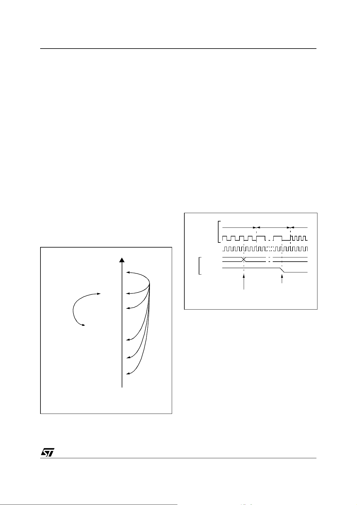
8 POWER SAVIN G MODES
ST72561
8.1 INTRODUCTION
To give a large measure of flexibility to the application in terms of power consumption, five main power saving modes are implemented in the ST7 (see
Figure 22):
■ Slow
■ Wait (and Slow-Wait)
■ Active Halt
■ Auto Wake up From Halt (AWUFH)
■ Halt
After a RESET the normal operating mode is selected by default (RUN mode). This mode drives
the device (CPU and embedded peripherals) by
means of a master clock which is based on the
main oscillator frequency divided or multiplied by 2
).
(f
OSC2
From RUN mode, the different power saving
modes may be selected by setting the relevant
register bits or by calling the specific ST7 software
instruction whose action depends on the oscillator
status.
Figure 22. Power Savin g Mo de Transitions
High
8.2 SLOW MODE
This mode has two targets:
– To reduce power consumption by decreasing the
internal clock in the device,
– To adapt the internal clock frequency (f
CPU
) to
the available supply voltage.
SLOW mode is controlled by three bits in the
MCCSR register: the SMS bit which enables or
disables Slow mode and two CPx bits which select
the internal slow frequency (f
In this mode, the master clock frequency (f
CPU
).
OSC2
can be divided by 2, 4, 8 or 16. The CPU and peripherals are clocked at this lower frequency
).
(f
CPU
Note: SLOW-WAIT mode i s activated by entering
WAIT mode while the device is in SLOW mode.
Figure 23. SLOW Mode Clock Transitions
f
f
CPU
f
OSC2
CP1:0
/2 f
OSC2
00 01
OSC2
/4 f
OSC2
)
RUN
SLOW
WAIT
SLOW WAIT
ACTIVE HALT
AUTO WAKE UP FROM HALT
HALT
POWER CONSUMPTION
Low
SMS
MCCSR
NORMALRUN MODE
NEW SLOW
FREQUENCY
REQUEST
REQUEST
39/262
Page 40
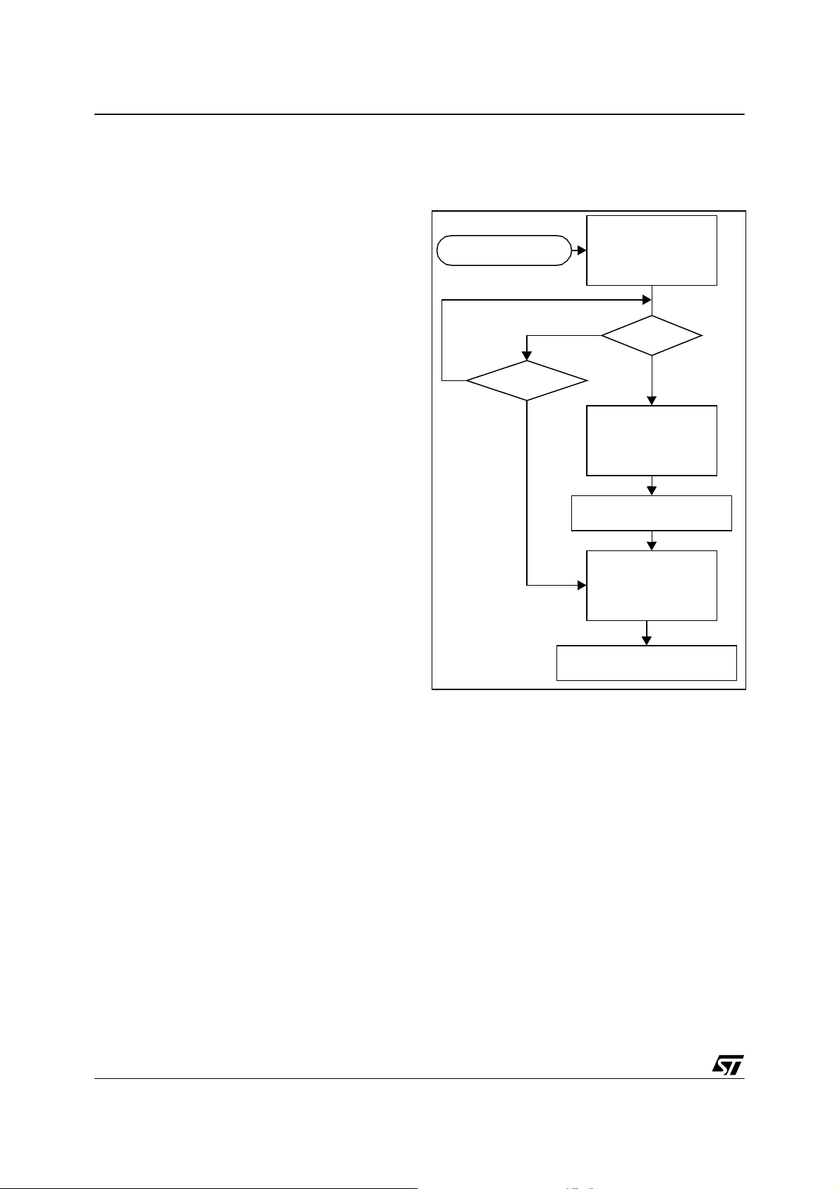
ST72561
POWER SAVING MODES (Cont’d)
8.3 WAIT MODE
WAIT mode places the MCU in a low power consumption mode by stopping the CPU.
This pow er s a v ing mo de is selected b y calling th e
‘WFI’ instruction.
All peripherals remain active. During WAIT mode,
the I[1:0] bits of the CC register are forced to ‘10’,
to enable all interrupts. All other registers and
memory remain unchanged. The MCU remains in
WAIT mode until an interrupt or RESET occurs,
whereupon the Program Counter branches to th e
starting address of the interrupt or Reset service
routine.
The MCU will r ema in in W AIT mod e unt il a R ese t
or an Interrupt occurs, causing it to wake up.
Refer to Figure 24.
Figure 24. WAIT Mode Flow-chart
OSCILLATOR
WFI INSTRUCTION
N
INTERRUPT
Y
PERIPHERALS
CPU
I[1:0] BITS
N
RESET
Y
OSCILLATOR
PERIPHERALS
CPU
I[1:0] BITS
256 OR 4096 CPU CLOCK
CYCLE DELAY
OSCILLATOR
PERIPHERALS
CPU
I[1:0] BITS
ON
ON
OFF
10
ON
OFF
ON
10
ON
ON
ON
XX
1)
FETCH RESET VECTOR
OR SERVICE INTERRUPT
Note:
1. Before servicing an interrupt , the CC register is
pushed on the stack. The I[1:0] bits of the CC register are set to the current software priority level of
the interrupt routine and recovered when the CC
register is popped.
40/262
Page 41
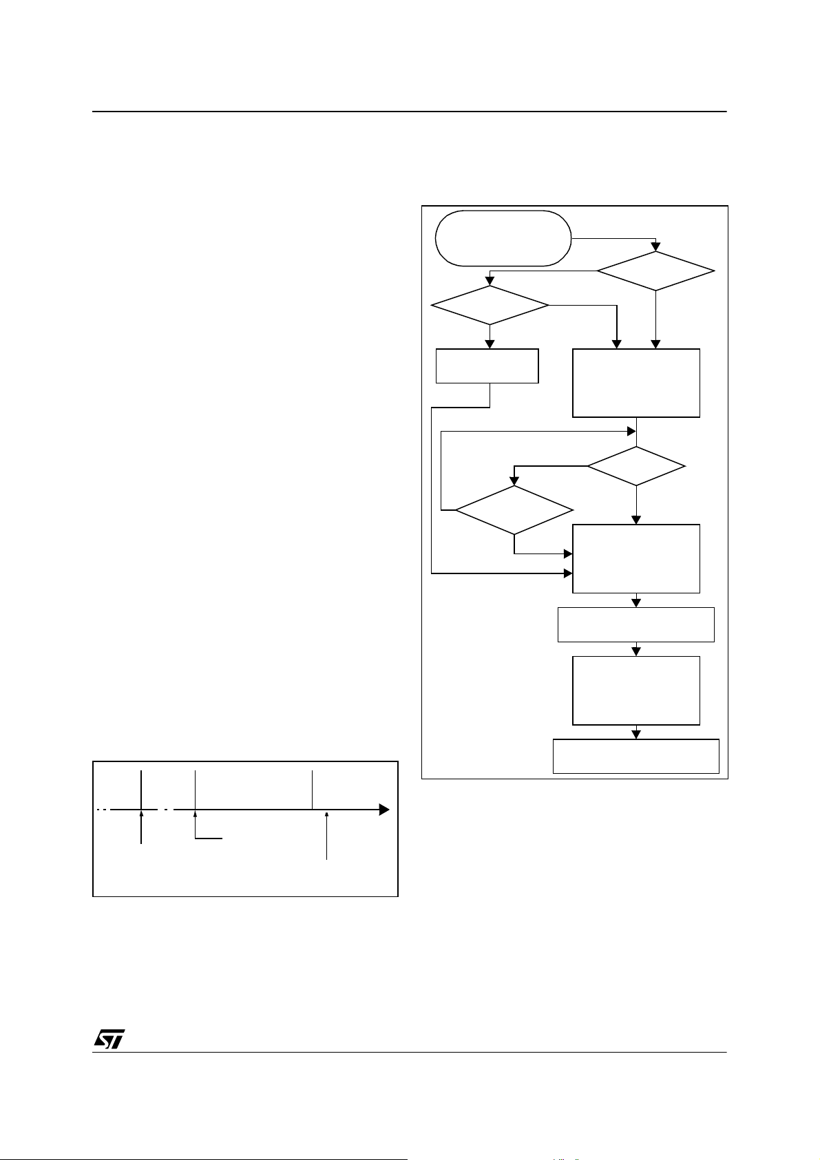
POWER SAVING MODES (Cont’d)
ST72561
8.4 HALT MODE
The HALT mode is the lowest power consumption
mode of the MCU. It is entered by executing the
‘HALT’ instruction when the OIE bit of the Main
Clock Controller Status register (MCCSR) is
cleared (see Section 10.2 on page 61 for more details on the MCCSR register) and when the
AWUEN bit in the AWUCSR register is cleared.
The MCU can exit HALT m ode on reception of e ither a specific interrupt (see Table 8, “Interrupt
Mapping,” on page 35) or a RESET. When exiting
HALT mode by means of a RESET or an interrupt,
the oscillator is immediately turned on and the 256
or 4096 CPU cycle delay is used to stabilize the
oscillator. After the start up delay, the CPU
resumes operation by servicing t he i nterrup t or by
fetching the reset vector which woke it up (see Fig-
ure 26).
When entering HALT mode, the I[1:0] bits in the
CC register are forced to ‘10b’to enable interrupts.
Therefore, if an interrupt is pending, the MCU
wakes up immediately.
In HALT mode, the main oscillator is turned off
causing all internal processing to be stopped, including the operation of the on-chip peripherals.
All peripherals are not clocked except the ones
which get their clock supply from another clock
generator (such as an external or auxiliary oscillator).
The compatibility of Watchdog operation with
HALT mode is configured by t he “WDGHALT” option bit of the option byte. The HALT instruction
when executed while the Watchdog system is enabled, can generate a Watchdog RESET (see
Section 14.1 on page 254 for m o r e d e tails) .
Figure 26. HALT Mode Flow-chart
HALT INSTRUCTION
(MCCSR.OIE=0)
(AWUCSR.AWUEN=0)
WATCHDOG
RESET
Y
CYCLE
WDGHALT
1
WATCHDOG
RESET
N
INTERRUPT
Y
1)
ENABLE
0
OSCILLATOR
PERIPHERALS
CPU
I[1:0] BITS
N
3)
OSCILLATOR
PERIPHERALS
CPU
I[1:0] BITS
256 OR 4096 CPU CLOCK
OSCILLATOR
PERIPHERALS
CPU
I[1:0] BITS
DISABLE
2)
DELAY
OFF
OFF
OFF
10
ON
OFF
ON
XX
ON
ON
ON
XX
4)
4)
Figure 25. HALT Timing Ove r v iew
HALTRUN RUN
HALT
INSTRUCTION
[MCCSR.OIE=0]
256 OR 4096 CPU
CYCLE DELAY
RESET
OR
INTERRUPT
FETCH
VECTOR
FETCH RESET VECTOR
OR SERVICE INTERRUPT
Notes:
1. WDGHALT is an option bit. See option byte sec-
tion for more details.
2. Peripheral clocked with an external clock source
can still be active.
3. Only some specific interrupts can exit the MCU
from HALT mode (such as ex ternal inte rrupt). Refer to Table 8, “Interrupt Mapping,” on pa ge 35 for
more details.
4. Before servicing an interrupt , the CC register is
pushed on the stack. The I[1:0] bits of the CC register are set to the current software priority level of
the interrupt routine and recovered when the CC
register is popped.
41/262
Page 42
ST72561
POWER SAVING MODES (Cont’d)
Halt Mode Recommendations
– Make sure that an external event is available to
wake up the microcontroller from Halt mode.
– When using an external interrupt to wake up the
microcontroller, reinitialize the corresponding I/O
as “Input Pull-up with Interrupt” before executing
the HALT instruction. The main reason for this is
that the I/O may be wrongly configured due to external interference or by an unforeseen logical
condition.
– For the same reason, reinitialize the level sensi-
tiveness of each external interrupt as a precautionary measure.
– The opcode for the HALT instruction is 0x8E. To
avoid an unexpected HALT instruction due to a
program counter failure, it is advised to clear all
occurrences of the data value 0x8E from memory. For example, avoid defining a constant in
ROM with the value 0x8E.
– As the HALT instruction clears the interrupt mask
in the CC register to allow interrupts, the user
may choose to clear all pending interrupt bits before executing the HALT instruction. This avoids
entering other peripheral interrupt routines after
executing the external interrupt routine corresponding to the wake-up event (reset or external
interrupt).
8.5 ACTIVE-HALT MODE
ACTIVE-HALT mode is the lowest power consumption mode of the MCU wi th a real time clock
available. It is entered by exec uting the ‘HALT’ instruction when MCC/RTC interrupt enable flag
(OIE bit in MCCSR register) is set and when the
AWUEN bit in the AWUCSR register is cleared
(See “Register Description” on page 46.)
MCCSR
OIE bit
Power Saving Mode entered when HALT
instruction is executed
0HALT mode
1 ACTIVE-HALT mode
The MCU can exit ACTIVE-HALT mode on reception of the RTC interrupt and some specific interrupts (see Table 8, “Interrupt Mapping,” on page
35) or a RESET. When exiting ACTIVE-HALT
mode by means of a RESET a 40 96 or 256 CPU
cycle delay occurs (depending on the option byte).
After the start up delay, the CPU resumes operation by servicing the interrupt or by fetching the reset vector which woke it up (see Fi gure 28).
When entering ACTIVE-HALT mode, the I[1:0] bits
in the CC register are cleared to enable interrupts.
Therefore, if an interrupt is pending, the MCU
wakes up immediately.
In ACTIVE-HALT mode, only the main oscillator
and its associated counter (MCC/RTC) are running to keep a wake-up time base. All other peripherals are not clocked except those which get their
clock supply from anot her clock generator (such
as external or auxiliary oscillator).
The safeguard against staying locked in A CTIVEHALT mode is provided by the oscillat or int er rupt.
Note: As soon as active halt is enabled, executing
a HALT instruction while the W atchdog is active
does not generate a RESET.
This means that the device cannot spend more
than a defined delay in this power saving mode.
42/262
Page 43
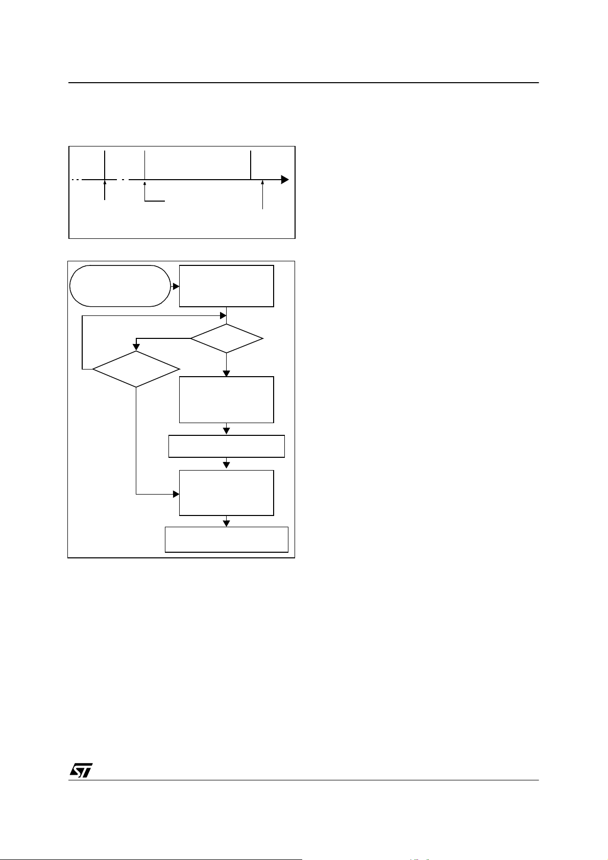
POWER SAVING MODES (Cont’d)
ST72561
Figure 27. ACTIVE-HALT Timing Overview
ACTIVE
HALTRUN RUN
HALT
INSTRUCTION
(Active Halt enabled)
256 OR 4096 CYCLE
DELAY (AFTER RESET)
RESET
OR
INTERRUPT
FETCH
VECTOR
Figur e 28. ACTIVE-HALT Mode Flow-chart
HALT INSTRUCTION
(MCCSR.OIE=1)
(AWUCSR.AWUEN=0)
N
INTERRUPT
Y
OSCILLATOR
PERIPHERALS
CPU
I[1:0] BITS
N
3)
OSCILLATOR
PERIPHERALS
CPU
I[1:0] BITS
RESET
Y
2)
ON
OFF
OFF
10
ON
OFF
ON
XX
Notes:
1. This delay occurs only if the MCU exits
ACTIVE-HALT mode by means of a RESET.
2. Peripheral clocked with an external clock
source can still be active.
3. Only the RTC interrupt and some specific interrupts can exit the MCU from ACTIVE-HALT
mode (such as external interrupt). Refer to
Table 8, “Interrupt Mapping,” on page 35 for
more details.
4. Before servicing an interrupt, the CC register is
pushed on the stack . The I[1:0] bits in the CC
register are set to the current software priority
level of the interrupt rou tine and res tored when
the CC register is popped.
4)
256 OR 4096 CPU CLOCK
CYCLE DELAY
OSCILLATOR
PERIPHERALS
CPU
I[1:0] BITS
FETCH RESET VECTOR
OR SERVICE INTERRUPT
ON
ON
ON
XX
4)
43/262
Page 44
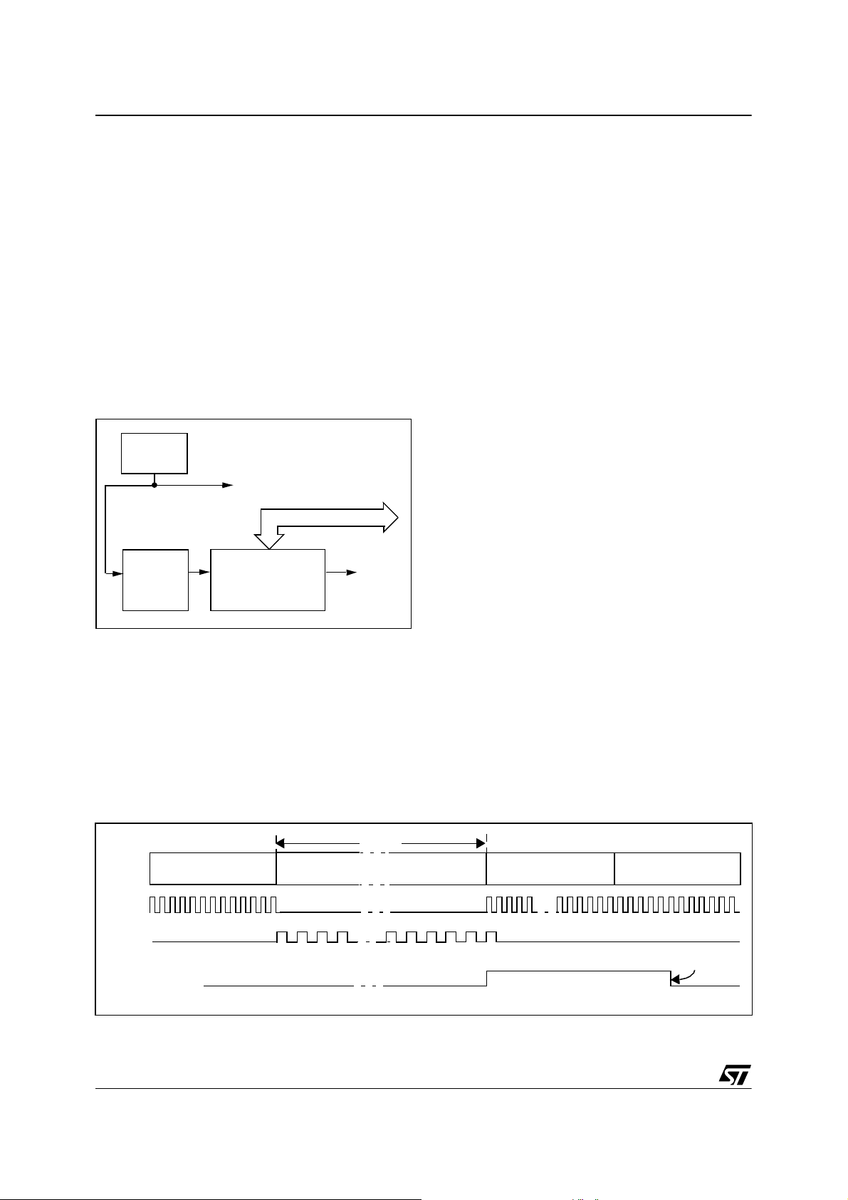
ST72561
POWER SAVING MODES (Cont’d)
8.6 AUTO WAKE UP FROM HALT MODE
Auto Wake Up From Halt (AWUFH) mode is similar to Halt mode with the addition of an internal RC
oscillator for wake-up. Compared to ACTIVEHALT mode, AWUFH has lower power consumption because the main clock is not kept running,
but there is no accurate realtime clock available.
It is entered by executing the HALT instruction
when the AWUEN bit in the AWUCSR register has
been set and the OIE bit in the MCCSR register is
cleared (see Section 10.2 on page 61 for more details).
Figure 29. AWUFH Mode Block Diagram
AWU RC
oscillator
f
AWU_RC
to Timer input capture
AWUFH
/64
divider
AWUFH
prescaler
/1 .. 255
interrupt
(ei0 source)
As soon as HALT mode is entered, and if the
AWUEN bit has been set in the AWUCSR register,
the AWU RC oscillator provides a clock signal
(f
AWU_RC
). Its frequency is divided by a fixed divider and a programmable prescaler controlled by the
AWUPR register. The output of this prescaler provides the delay time. When the delay has elapsed
the AWUF flag is set by hardware and an interrupt
wakes-up the MCU from Halt mode . At the sam e
time the main oscillator is immediately turned o n
and a 256 or 4096 cycle delay is used to stabilize
it. After this start-up delay, the CPU resumes operation by servicing the AWUFH interrupt. The AWU
flag and its associated interrupt are cleared by
software reading the AWUCSR register.
To compensate for any frequency dispersion of
the AWU RC oscillator, it can be calibrated by
measuring the clock fre quency f
AWU_RC
and then
calculating the right prescaler value. Measurement
mode is enabled by s etting the AWUM bit in the
AWUCSR register in Run mode. This connects
f
AWU_RC
lowing the f
to the ICAP1 input of the 16-bit timer, al-
AWU_RC
to be measured using the main
oscillator clock as a reference timebase.
Similarities with Halt mode
The following AWUFH mode behaviour is the
same as normal Halt mode:
– The MCU can exit AWUFH mode by means of
any interrupt with exit from Halt capability or a reset (see Section 8.4 "HALT MODE").
– When entering AWUFH mode, the I[1:0] bits in
the CC register are forced to 10b to enable interrupts. Therefore, if an interrupt is pending, the
MCU wakes up immediately.
– In AWUFH mode, the main oscillator is turned off
causing all internal processing to be stopped, including the operation of the on-chip peripherals.
None of the peripherals are clocked except those
which get their clock supply from another clock
generator (such as an external or auxiliary oscillator like the AWU osc illator).
– The com patibility of Watchdog ope ration with
AWUFH mode is configured by the WDGHALT
option bit in the option byte. Depending on this
setting, the HALT instruction when executed
while the Watchdog system is enabled, can generate a Watchd og R ESET .
Figure 30. AWUF Halt Timing Diagram
RUN MODE HALT MO DE 256 or 4096 t
f
CPU
f
AWU_RC
AWUFH interrupt
44/262
t
AWU
CPU
RUN MODE
Clear
by software
Page 45
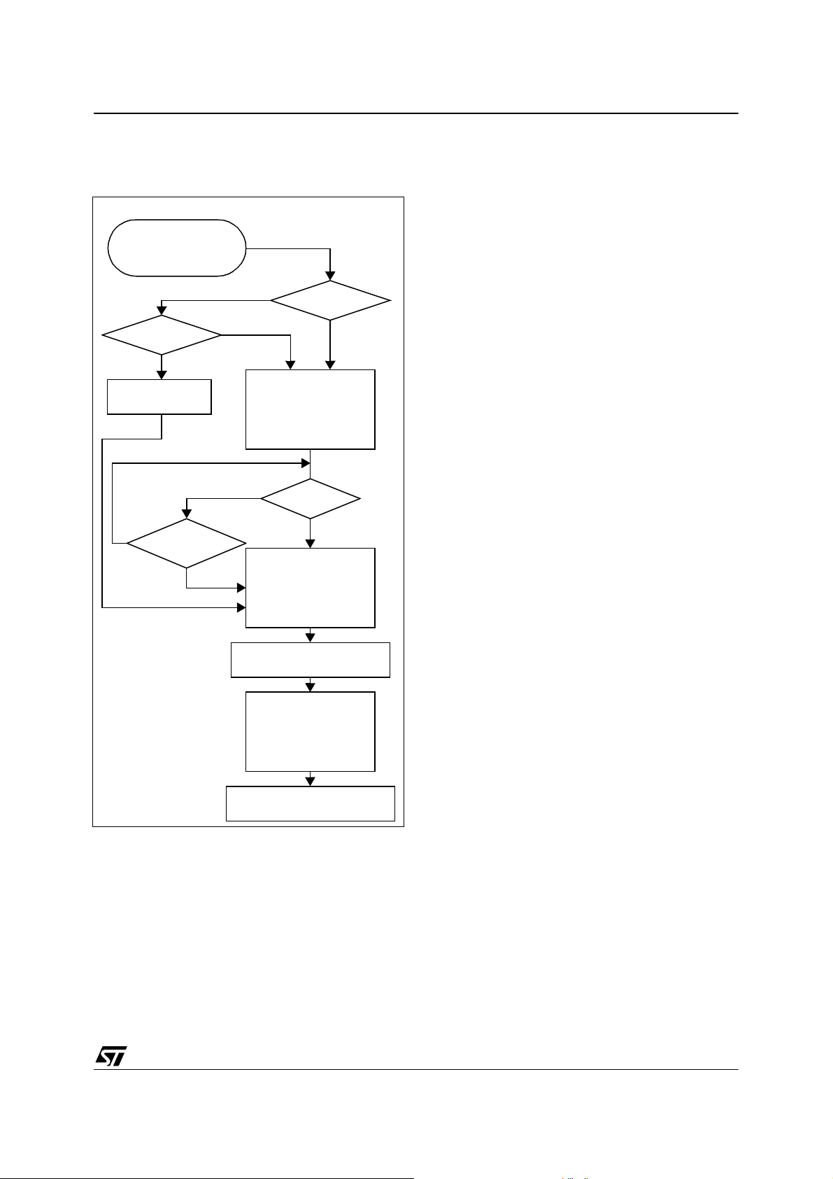
POWER SAVING MODES (Cont’d)
Figure 31. AWUFH Mode Flow-chart Notes:
1. WDGHALT is an option bit. See option byte sec-
tion for more details.
HALT INSTRUCTION
(MCCSR.OIE=0)
(AWUCSR.AWUEN=1)
2. Peripheral clocked with an external clock source
can still be active.
3. Only an AWUFH interrupt and some specific in-
ENABLE
WATCHDOG
terrupts can exit the MCU from HALT m ode (suc h
as external interrupt). Refer to Table 8, “Interrupt
Mapping,” on page 35 for more d e ta ils.
WDGHALT
1)
0
DISABLE
4. Before servicing an interrupt , the CC register is
pushed on the stack. The I[1:0] bits of the CC reg-
1
WATCHDOG
RESET
AWU RC OSC ON
MAIN OSC
PERIPHERALS
CPU
I[1:0] BITS
2)
OFF
OFF
OFF
10
ister are set to the current software priority level of
the interrupt routine and recovered when the CC
register is popped.
ST72561
N
INTERRUPT
Y
N
3)
AWU RC OSC OFF
MAIN OSC
PERIPHERALS
CPU
I[1:0] BITS
256 OR 4096 CPU CLOCK
AWU RC OSC OFF
MAIN OSC
PERIPHERALS
CPU
I[1:0] BITS
FETCH RESET VECTOR
OR SERVICE INTERRUPT
RESET
Y
CYCLE
DELAY
ON
OFF
ON
XX
ON
ON
ON
XX
4)
4)
45/262
Page 46
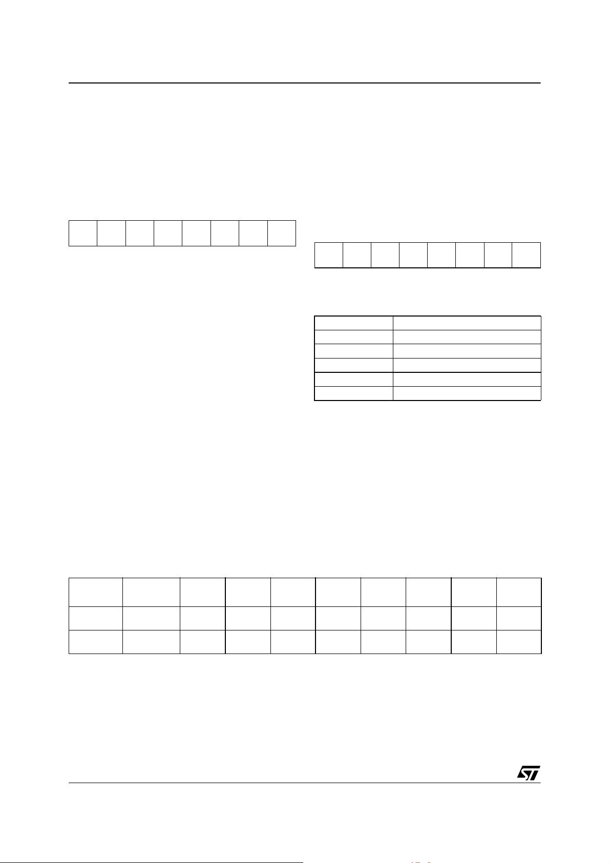
ST72561
POWER SAVING MODES (Cont’d)
8.6.0.1 Register Description
AWUFH CONTROL/STATUS REGISTER
(AWUCSR)
Read/Write (except bit 2 read only)
Reset Value: 0000 0000 (00h)
70
0: AWUFH (Auto Wake Up From Halt) mode disa-
bled
1: AWUFH (Auto Wake Up From Halt) mode ena-
bled
AWUFH PRESCALER REGISTER (AWUPR)
Read/Write
Reset Value: 1111 1111 (FFh)
00000
AWUFAWUMAWU
EN
Bits 7:3 = Reserved.
Bit 2= AWUF Auto Wake Up Flag
This bit is set by hardware when the AWU module
generates an interrupt and cleared by software on
reading AWUCSR.
0: No AWU interrupt occurred
1: AWU interrupt occurred
Bit 1= AWUM Au to Wake Up Measur ement
This bit enables the A WU RC oscillat or and connects its output to the ICAP1 input of the 16-bit timer. This allows the timer to be used to measure the
AWU RC oscillator dispersion and then compensate this dispersion by providing the right value in
the AWUPR register.
0: Measurement disabled
1: Measurement enabled
Bit 0 = AWUEN Auto Wake Up From Halt Enabled
This bit enables the Auto Wake Up From Halt feature: once HALT mode is entered, the AWUFH
wakes up the microcontroller after a time delay defined by the AWU prescaler value. It is set and
cleared by software.
70
AWU
AWU
AWU
AWU
AWU
AWU
AWU
AWU
PR7
PR6
PR5
PR4
PR3
PR2
PR1
PR0
Bits 7:0= AWUPR[7:0] Auto Wake Up Prescaler
These 8 bits define the AWUPR Dividing factor (as
explained below:
AWUPR[7:0
00h Forbidden (See note)
01h 1
FEh 254
FFh 255
] Dividing factor
... ...
In AWU mode, the p eriod that the MCU stays in
Halt Mode (t
t
AWU
in Figure 30) is defined by
AWU
64 AWUPR×
1
--------------------------t
f
AWURC
+×=
RCSTRT
This prescaler register can be programmed to
modify the time that t he MCU sta ys in Halt mode
before waking up automatically.
Note: If 00h is written to AWUPR, depending on
the product, an interrupt is generated imm ediately
after a HALT instruction, or the AWUPR remains
inchanged.
Table 10. AWU Register Map and Reset Values
Address
(Hex.)
002Bh
002Ch
46/262
Register
Label
AWUCSR
Reset Value
AWUPR
Reset Value
76543210
00000
AWUPR71AWUPR61AWUPR51AWUPR41AWUPR31AWUPR21AWUPR11AWUPR0
AWUF0AWUM0AWUEN
0
1
Page 47
9 I/O PORTS
ST72561
9.1 INTRODUCTION
The I/O ports offer different functional modes:
– transfer of data through digital inputs and outputs
and for specific pins:
– external interrupt generation
– alternate signal input/output for the on-chip pe-
ripherals.
An I/O port contains up to 8 pins. Each pin can be
programmed independently as digital input (with or
without interrupt generation) or digital output.
9.2 FUNCTIONAL DESCRIPTION
Each port has 2 main registers:
– Data Register (DR)
– Data Direction Register (DDR)
and one optional register:
– Option Register (OR)
Each I/O pin may be programmed using the corre-
sponding register bits in the DDR and OR registers: bit X corresponding to pin X of the port. The
same correspondence is used for the DR register.
The following description takes into account the
OR register, (for specific ports which do not provide this register refer to the I/O Port Implem entation section). The generic I/O block diagram is
shown in Figure 32
9.2.1 Input Modes
The input configuration is sele cted by clearing the
corresponding DDR register bit.
In this case, reading the DR register returns the
digital value applied to the external I/O pin.
Different input modes can be selected by software
through the OR register.
Notes:
1. Writing the DR register modifies the latc h valu e
but does not affect the pin status.
2. When switching from input to output mode, the
DR register has to be written first to drive the correct level on the pin as soon as the port is configured as an output.
3. Do not use read/modify/write instructions (BSET
or BRES) to modify the DR register
External interrupt function
When an I/O is configured as Input with Interrupt,
an event on this I/O can generate an external interrupt request to the CPU.
Each pin can independen tly generate an i nterrupt
request. The interrupt sensitivity is independently
programmable using the sensitivity bits in the
EICR register.
Each external interrupt vector is linked to a d edicated group of I/O port pins (see pinout description
and interrupt section). If several inpu t pins are s elected simultaneously as i nterrupt sources, these
are first detected according to the sensitivity bits in
the EICR register and then logically ORed.
The external interrupts are hardware interrupts,
which means that the request latch (not accessible
directly by the application) is automatically cleared
when the corresponding interrupt vector is
fetched. To clear an unwanted pending interrupt
by software, the sensitivity bits in the EICR register
must be modified.
9.2.2 Output Modes
The output configuration is selecte d by se tting the
corresponding DDR register bit. In this case, writing the DR register applies this digital value to the
I/O pin through the latch. Then reading the DR register returns the previously stored value.
Two different output modes can be selected by
software through the OR register: Output push-pull
and open-drain.
DR register value and output pin status:
DR Push-pull Open-drain
0V
1V
SS
DD
Vss
Floating
9.2.3 Alternate Functions
When an on-chip peripheral is configured to use a
pin, the alternate function is automat ically selected. This alternate function takes priority over the
standard I/O programming.
When the signal is coming from an on-chip peripheral, the I/O pin is automati cally conf igured in ou tput mode (push-pull or open drain according to the
peripheral).
When the signal is going t o an on-c hip pe ripheral,
the I/O pin must be configured in input mode. In
this case, the pin state is also digitally readable by
addressing the DR register.
Note: Input pull-up configuration can cause unexpected value at the input of the alternate peripheral
input. When an on-chip peripheral use a pin as input and output, this pin h as to be c on figured in input floating mode.
47/262
Page 48
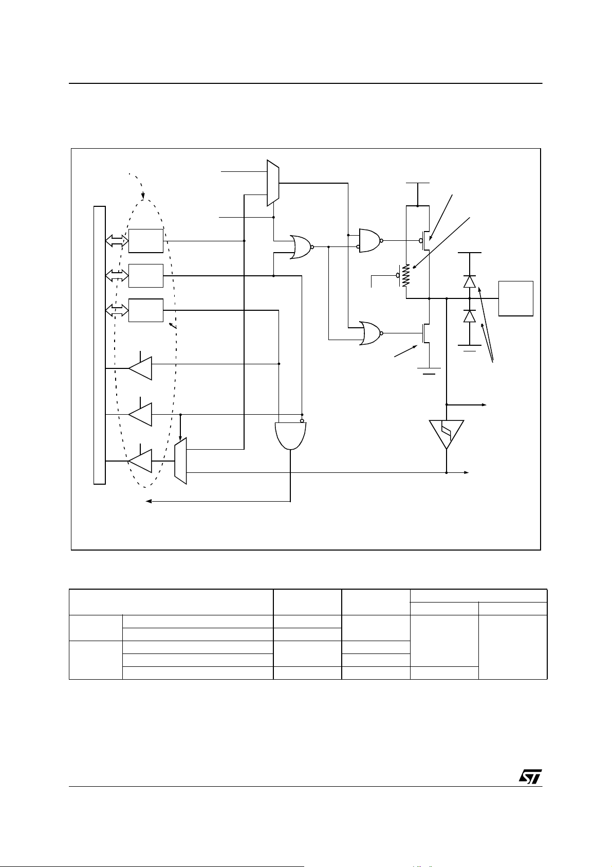
ST72561
I/O PORTS (Cont’d)
Figure 32. I/O Por t Ge neral B lo ck D iag ram
REGISTER
ACCESS
DATA BUS
DDR SEL
DR
DDR
OR
OR SEL
DR SEL
ALTERNATE
OUTPUT
ALTERNATE
ENABLE
If implemented
1
1
0
PULL-UP
CONDITION
N-BUFFER
V
DD
CMOS
SCHMITT
TRIGGER
P-BUFFER
(see table below)
PULL-UP
(see table below)
V
DD
PAD
DIODES
(see table below)
ANALOG
INPUT
0
EXTERNAL
INTERRUPT
SOURCE (eix)
Table 11. I/O Port Mode Options
Configuration Mode Pull -Up P-Buffe r
Input
Output
Floating with/without Interrupt Off
Pull-up with/withou t Interrupt On
Push-pull
Open Drain (logic level) Off
True Open Drain NI NI NI (see note)
Legend: NI - not implemented
Off - implemented not activated
On - implemented and activated
ALTERNATE
INPUT
Diodes
to V
DD
Off
Off
On
Note: The diode to V
true open drain pads. A local protection between
the pad and V
vice against positive stress.
is implemented to protect the de-
SS
On
is not implemented in the
DD
to V
SS
On
48/262
Page 49
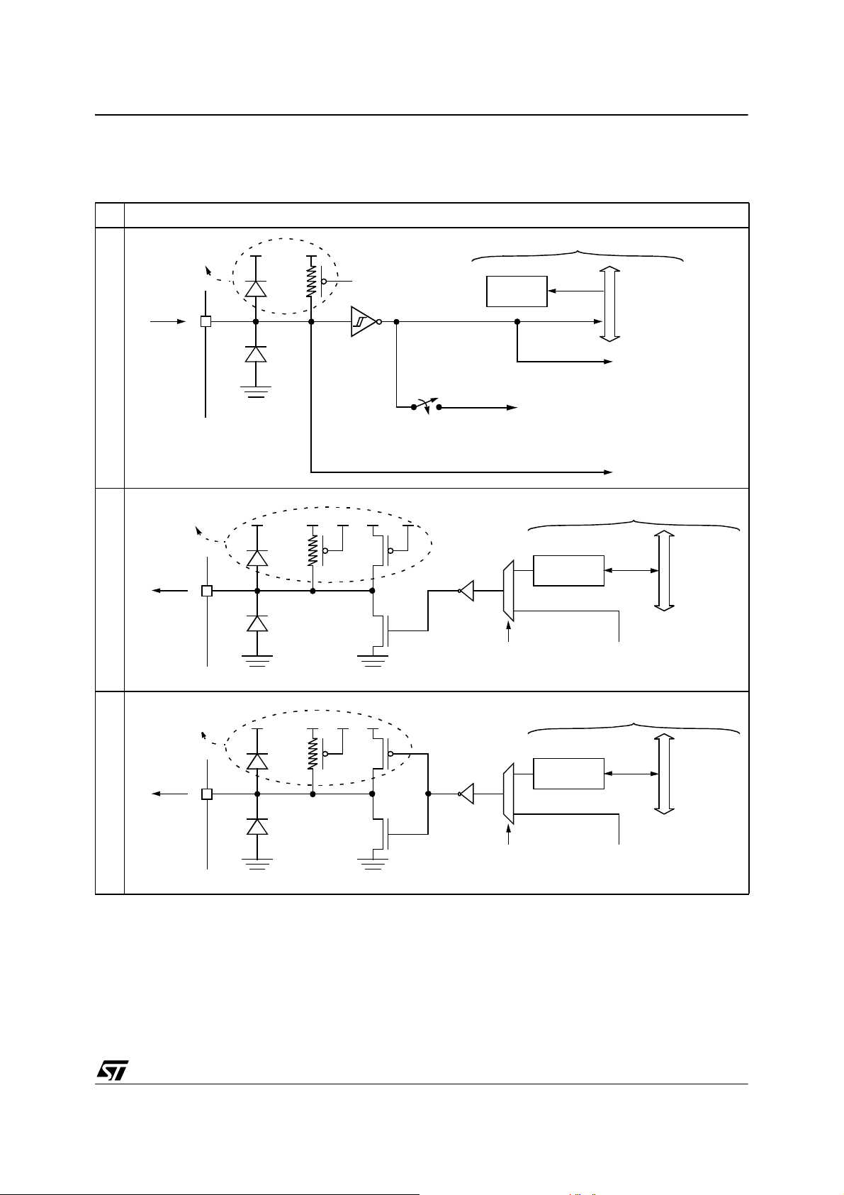
I/O PORTS (Cont’d)
Table 12. I/O Port Configurations
ST72561
Hardware Configuration
NOT IMPLEMENTED IN
TRUEOPEN DRAIN
I/O PORTS
1)
INPUT
NOT IMPLEMENTED IN
TRUE OPEN DRAIN
2)
I/O PORTS
OPEN-DRAIN OUTPUT
PAD
PAD
V
DD
R
PU
V
DD
R
PU
PULL-UP
CONDITION
INTERRUPT
CONDITION
DR REGISTER ACCESS
DR
REGISTER
EXTERNAL INTERRUPT
SOURCE (ei
ENABLE OUTPUT
W
R
)
x
DR REGISTER ACCESS
DR
REGISTER
ALTERNATEALTERNATE
ALTERNATEINPUT
ANALOG INPUT
R/W
DAT A BUS
DAT A BUS
NOT IMPLEMENTED IN
TRUE OPEN DRAIN
2)
I/O PORTS
PUSH-PULL OUTPUT
PAD
V
DD
R
PU
ENABLE OUTPUT
DR REGISTER ACCESS
DR
REGISTER
ALTERNATEALTERNATE
R/W
DAT A BUS
Notes:
1. When the I/O port is in input configuration and the associated alternate function is enabled as an output,
reading the DR register will read the alternate function outp ut status.
2. When the I/O port is in output configuration and t he associated alternate function is enabled as an input,
the alternate function reads the pin status given by the DR register content.
49/262
Page 50
ST72561
I/O PORTS (Cont’d)
CAUTION: The alternate function must not be ac -
tivated as long as the pin is configured as input
with interrupt, in order to avoid generating spurious
interrupts.
Analog alternate function
When the pin is used as an ADC input, the I/O
must be configured as floating input. The analo g
multiplexer (controlled by the ADC registers)
switches the analog voltage present on the selected pin to the common analog rail which is connected to the ADC input.
It is recommended not to change the voltage level
or loading on any port pin while conversion is in
progress. Furthermore it i s recommended not to
have clocking pins located close t o a selected analog pin.
WARNING: The analog input voltage level must
be within the limits stated in the absolute maximum r a tings.
9.3 I/O PORT IMPLEMENTATION
The hardware implementation on each I/O port depends on the settings in the DDR and OR regi sters
and specific feature of the I/O port such as ADC Input or true open drain.
Switching these I/O ports from one state to another should be done in a sequence that prevents unwanted side effects. Recommended safe transitions are illustrated in Figure 33 Other transitions
are potentially risky and shou ld be avoide d, since
they are likely to present unwanted side-effects
such as spurious interrupt generation.
Figure 33. Interrupt I/O Port State Transitions
01
INPUT
floating/pull-up
interrupt
00
INPUT
floating
(reset state)
10
OUTPUT
open-drain
XX
11
OUTPUT
push-pull
= DDR, OR
9.4 LOW POWER MODES
Mode Description
WAIT
HALT
No effect on I/O ports. External interrupts
cause the device to exit from WAIT mode.
No effect on I/O ports. External interrupts
cause the device to exit from HALT mode.
9.5 INTERRUPTS
The external interrupt event generates an interrupt
if the corresponding configuration is selected with
DDR and OR registers and the interrupt mask in
the CC register is not active (RIM instruction).
Interrupt Event
External interrupt on
selected external
event
Event
Flag
-
Enable
Control
Bit
DDRx
ORx
Exit
from
Wait
Yes Yes
Exit
from
Halt
50/262
Page 51
I/O PO R T S (Cont’d)
9.6 I/O Port Implementation
The I/O port register configurations are summarised as following.
9.6.1 Standard Ports
PB7:6, PC0, PC3, PC7:5, PD3:2, PD5, PE7:0,
PF7:0
MODE DDR OR
floating input 0 0
pull-up input 0 1
open drain output 1 0
push-pull output 1 1
9.6.2 Interrupt Ports
PA0,2,4,6; PB0,2,4; PC1; PD0,6
(with pull-up)
MODE DDR OR
floating input 0 0
pull-up interrupt input 0 1
open drain output 1 0
push-pull output 1 1
ST72561
PA1,3,5,7; PB1,3,5; PC2; PD1,4,7
(without pull-up)
MODE DDR OR
floating input 0 0
floating interrupt input 0 1
open drain output 1 0
push-pull output 1 1
9.6.3 Pull-up Input Port (CANTX requirement)
PC4
MODE
pull-up input
The PC4 port cannot be controlled by DR/DDR/
OR in output. The CAN peripheral controls it directly when enabled. Otherwise, it is pull-up input.
However, it is still possible to read the port through
DR register (providing DDR is set properly).
51/262
Page 52
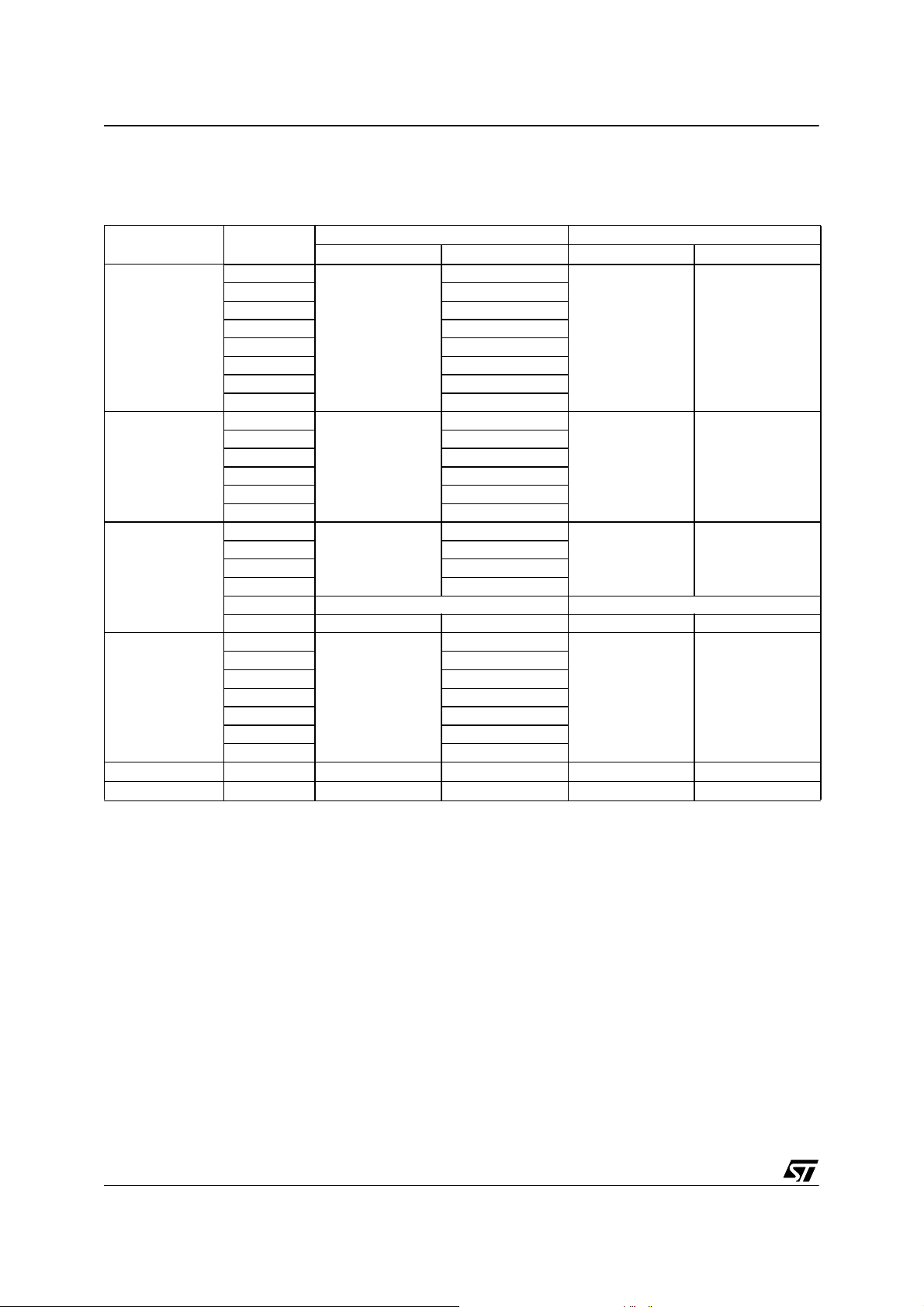
ST72561
I/O PO R T S (Cont’d)
Table 13. Port Configuration
Port Pin name
PA0
PA1 floating interrupt (ei0)
PA2 pull- up interr upt (ei0 )
Port A
Port B
Port C
Port D
PA3 floating interrupt (ei0)
PA4 pull- up interr upt (ei0 )
PA5 floating interrupt (ei0)
PA6 pull- up interr upt (ei0 )
PA7 floating interrupt (ei0)
PB0
PB1 floating interrupt (ei1)
PB2 pull- up interr upt (ei1 )
PB3 floating interrupt (ei1)
PB4 pull- up interr upt (ei1 )
PB5 floating interrupt (ei1)
PC0
PC1 pull-up in t e rrupt (ei2 )
PC2 floati ng interrupt (ei2)
PC3 pull-up
PC4 pull-up controll ed by CANTX *
PC7:5 floating pull-up open drain push-pull
PD0
PD1 floati ng interrupt (ei3)
PD3:2 pull-up
PD4 floati ng interrupt (ei3)
PD5 pull-up
PD6 pull-up in t e rrupt (ei3 )
PD7 floati ng interrupt (ei3)
OR = 0 OR = 1 OR = 0 OR = 1
floating
floating
floating
floating
Port E PE7:0 floating (TTL) pull-up (TTL) open drain push-pull
Port F PF7:0 floating (TTL) pull-up (TTL) open drain push-pull
Input Output
pull-up interrupt (ei0)
open drain push-pull
pull-up interrupt (ei1)
open drain push-pull
pull-up
open drain push-pull
pull-up interrupt (ei3)
open drain push-pull
* Note: when the CANTX alternate function is selected, the I/O port operates in output push-pull mode.
52/262
Page 53
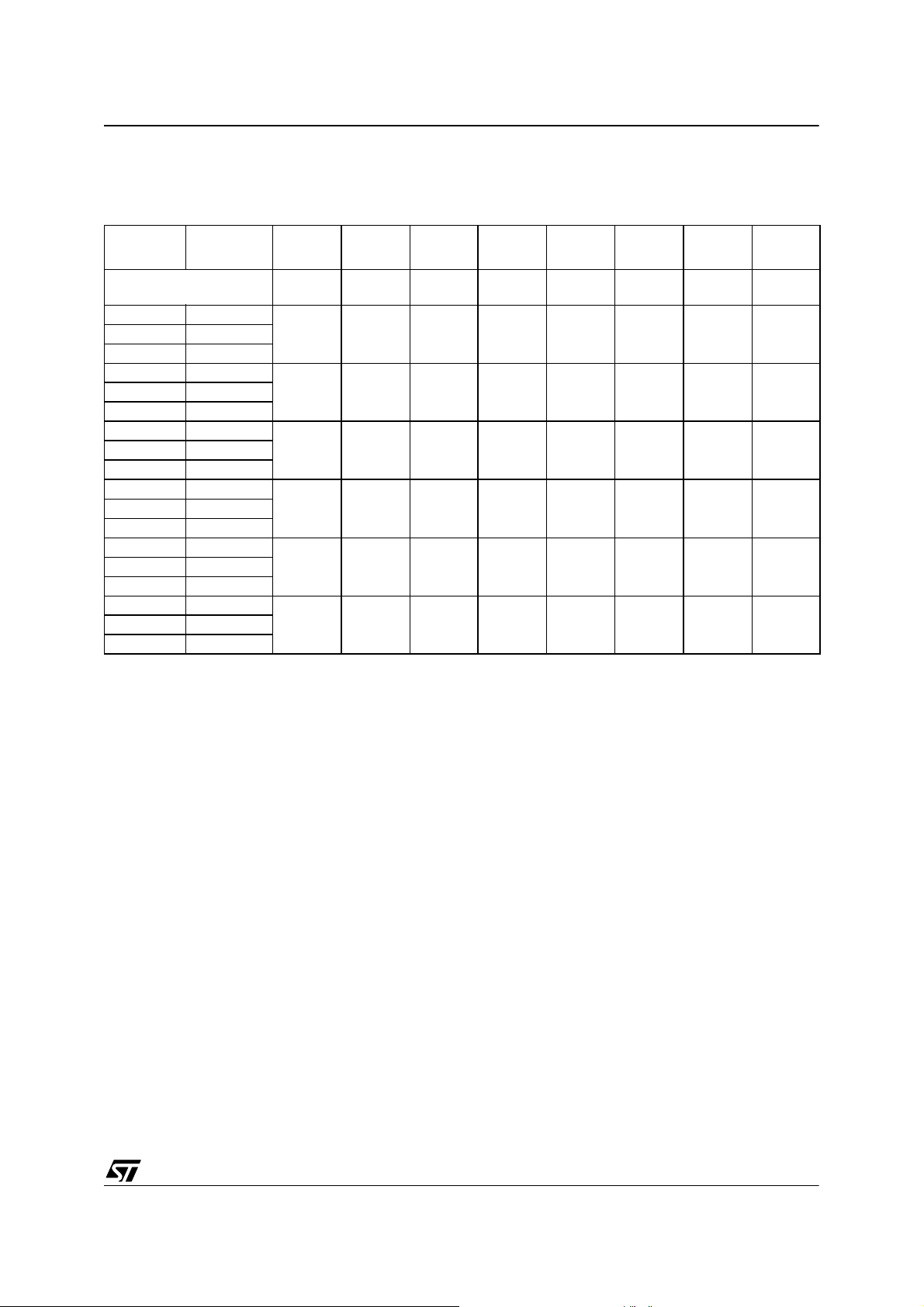
I/O PORTS (Cont’d)
Table 14. I/O Port Register Map and Reset Values
ST72561
Address
(Hex.)
Reset Value
of all IO port registers
0000h PADR
0002h PAOR
0003h PBDR
0005h PBOR
0006h PCDR
0008h PCOR
0009h PDDR
000Bh PDOR
000Ch PEDR
000Eh PEOR
000Fh PFDR
0011h PFOR
Register
Label
76543210
00000000
MSB LSB0001h PADDR
MSB LSB0004h PBDDR
MSB LSB0007h PCDDR
MSB LSB000Ah PDDDR
MSB LSB000Dh PEDDR
MSB LSB0010h PFDDR
53/262
Page 54
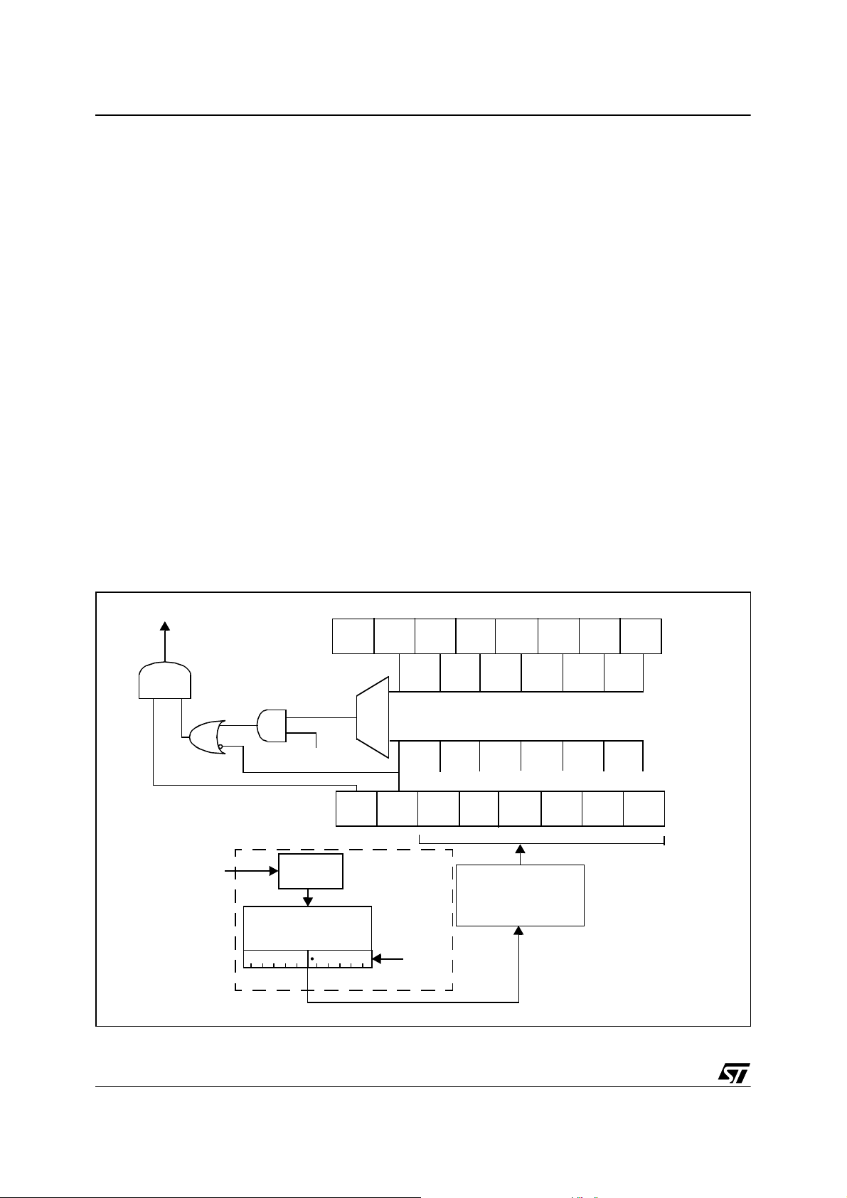
ST72561
10 ON-CHIP PER IPHERALS
10.1 WINDOW WATCHDOG (WWD G)
10.1.1 Introduction
The Window Watchdog is used t o detect the occurrence of a software fault, usually generated by
external interference or by unforeseen logical conditions, which causes the application program to
abandon its normal seque nce. The Watchdo g circuit generates an MCU reset o n expiry of a programmed time period, unless the program refreshes the contents of the downcounter before t he T6
bit becomes cleared. An MCU reset is also generated if the 7-bit downcounter value (in the control
register) is refreshed before the downco unter has
reached the window register value. This implies
that the counter must be refreshed in a limited window.
10.1.2 Main Features
– Programm able free-running down co unter
– Conditional reset
– Reset (if watchdog activated) when the down-
counter value becomes less than 40h
– Reset (if watchdog activated) if the down-
Figure 34. Watchdog Block Diagram
RESET
-
W6
counter is reloaded outside the window (see
Figure 37)
– Hardware/S oftware Watc hdog activation (se-
lectable by option byte)
– Optional reset on HALT instruction (configurable
by option byte)
10.1.3 Functional Description
The counter value stored in the WDGCR register
(bits T[6:0]), is decremented every 16384 f
OSC2
cycles (approx.), and the length of the timeout period can be programmed by the use r in 64 increments.
If the watchdog is activated (the WDGA bit is set)
and when the 7-bit downcounter (T[6:0] bits) rolls
over from 40h to 3Fh (T6 b ecome s cl eared), it initiates a reset cycle pulling low the reset pin for typically 30µs. If the software reloads the counter
while the counter is greater than the value stored
in the window register, then a reset is generated.
WATCHDOG WINDOW REGISTER (WDGWR)
W5
W4
W3
W2
W1
W0
54/262
f
OSC2
Write WDGCR
MCC/RTC
RTC COUNTER
MSB
11
comparator
=1 when
T6:0 > W6:0
DIV 64
12-BIT MCC
LSB
56
CMP
WDGA
0
WATCHDOG CONTROL REGISTER (WDGCR)
T5
T6
TB[1:0] bits
(MCCSR
Register)
T4
T3
6-BIT DOWNCOUNTER (CNT)
WDG PRESCALE R
DIV 4
T2
T1
T0
Page 55

WINDOW WATCHDOG (Cont’d)
The application program must write in the
WDGCR register at regular intervals during normal
operation to prevent an MCU reset. This operation
must occur only when the counter value is lower
than the window register value. The value to b e
stored in the WDGCR register must be between
FFh and C0h (see Figure 35):
– Enabling the watchdog:
When Software Watchdog is selected (by option
byte), the watchdog is disabled after a reset. It is
enabled by setting the WDGA bit in the WDGCR
register, then it cannot be disabled again except
by a reset.
When Hardware Watchdog is selected (by option
byte), the watchdog is always active and the
WDGA bit is not used.
– Controlling the downcounter :
This downcounter is free-running: it counts down
even if the watchdog is disabled. When the
watchdog is enabled, the T6 bit must be set to
prevent generating an immediate reset.
The T[5:0] bits contain the number of increments
which represents the time delay before the
watchdog produces a reset (see Figure 35. Ap-
proximate Timeout Duration). The timing varies
ST72561
between a minimum and a maximum value due
to the unknown status of the prescaler when writing to the WDGCR register (see Figure 36).
The window register (WDGWR) contains the
high limit of the window: to prevent a reset, the
downcounter must be reloaded when its value is
lower than the window register value and greater
than 3Fh. Figure 37 describes the window watchdog process.
Note: The T6 bit can be used to generate a s oftware reset (the WDGA bit is set and t he T6 bit is
cleared).
– Watc hdog Reset on Halt option
If the watchdog is activated and the watchdog reset on halt option is selected, then the HALT instruction will generate a Reset.
10.1.4 Using Halt Mode with the WDG
If Halt mode with Watchdog is en abled by option
byte (No watchdog reset on HALT instruction), it is
recommended before executing the HALT instruction to refresh the WDG counter, to avoid an unexpected WDG reset immediately after waking up
the microcontroller.
55/262
Page 56

ST72561
WINDOW WATCHDOG (Cont’d)
10.1.5 How to Program the Watchdog Timeout
Figure 3 5 shows the linear relationship between
the 6-bit value to be loaded in the Watchdog Counter (CNT) and the resulting timeout duration in milliseconds. This can be used for a quick calculation
without taking the timing variations into account. If
Figure 35. Approximate Timeout Duration
3F
38
30
28
more precision is needed, use the formulae in Fig-
ure 36.
Caution: When writing to the WDGCR register, always write 1 in the T6 bit to avoid generating an
immediate reset.
20
18
CNT Value (hex.)
10
08
00
1.5 65
503418 82 98 114
Watchdog timeout (ms) @ 8 MHz. f
128
OSC2
56/262
Page 57
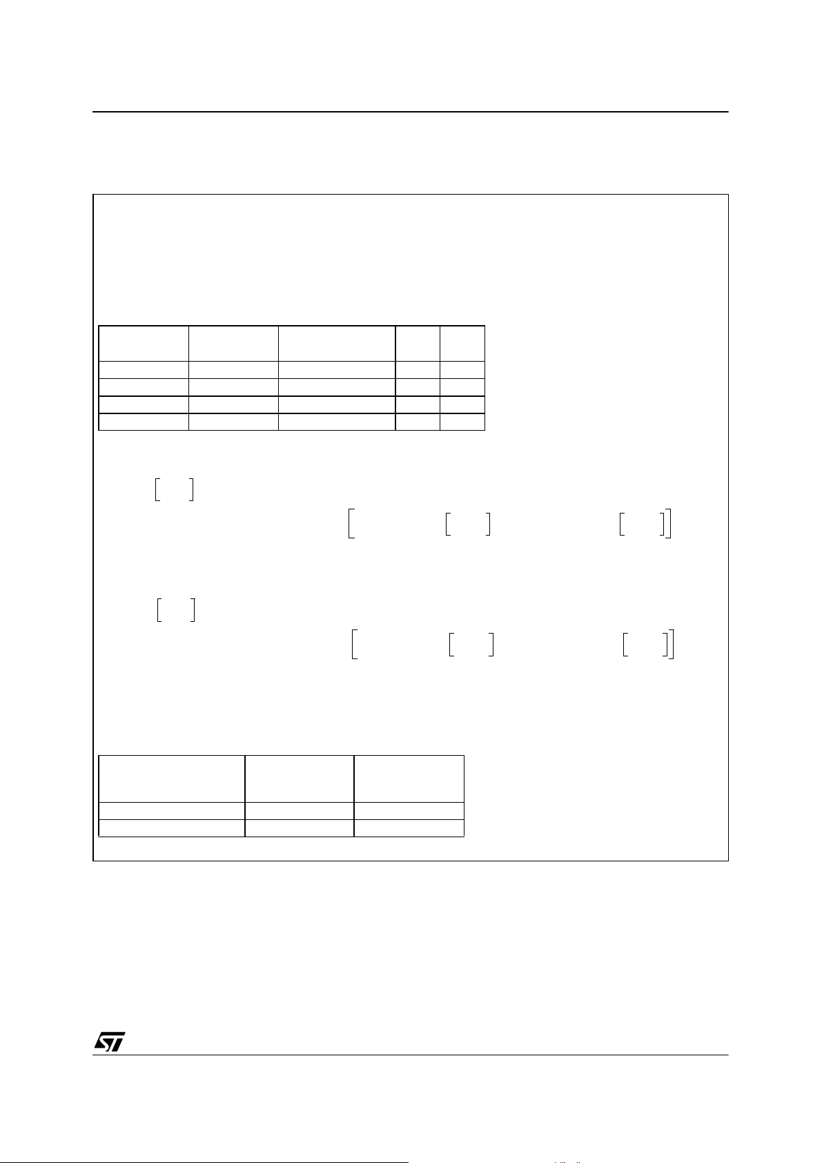
WATCHD OG TI M E R (Cont’d)
ST72561
Figure 36. Exact Timeout Duration (t
min
and t
max
)
WHERE:
= (LSB + 128) x 64 x t
t
min0
t
= 16384 x t
max0
t
OSC2
= 125ns if f
OSC2
OSC2
OSC2
=8 MHz
CNT = Value of T[5:0] bits in the WDGCR register (6 bits)
MSB and LSB are values f rom th e table b elow depending on the timeba se selecte d by t he T B[1:0] bits
in the MCCSR register
TB1 Bit
(MCCSR Reg.)
0 0 2ms 4 59
0 1 4ms 8 53
1 0 10ms 20 35
1 1 25ms 49 54
To calculate the m i ni m um W at chdog Tim eout (t
IF THEN
CNT
<
MSB
------------4
To calculate the maximum Watchdog Timeout (t
TB0 Bit
(MCCSR Reg.)
t
ELSE
t
mintmin0
Selected MCCSR
Timebase
mintmin0
MSB LSB
):
min
16384 CNT t
16384 CNT
× 192 LSB+()64
××+=
osc2
max
–
):
4CNT
---------------- MSB
+ t
××
4CNT
---------------- MSB
×+=
osc2
IF THEN
CNT
MSB
-------------
≤ t
4
ELSE
maxtmax0
t
maxtmax0
16384 CNT t
16384 CNT
× 192 LS B+()64
××+=
osc2
–
4CNT
---------------- MSB
+ t
××
4CNT
---------------- MSB
Note: In the above formulae, division results must be rounded down to the next integer value.
Example:
With 2ms timeout selected in MCCSR register
Value of T[5:0] Bits in
WDGCR Register (Hex.)
00 1.496 2.048
3F 128 128.552
Min. Watchdog
Timeout (ms)
t
min
Max. Watchdog
Timeout (ms)
t
max
×+=
osc2
57/262
Page 58
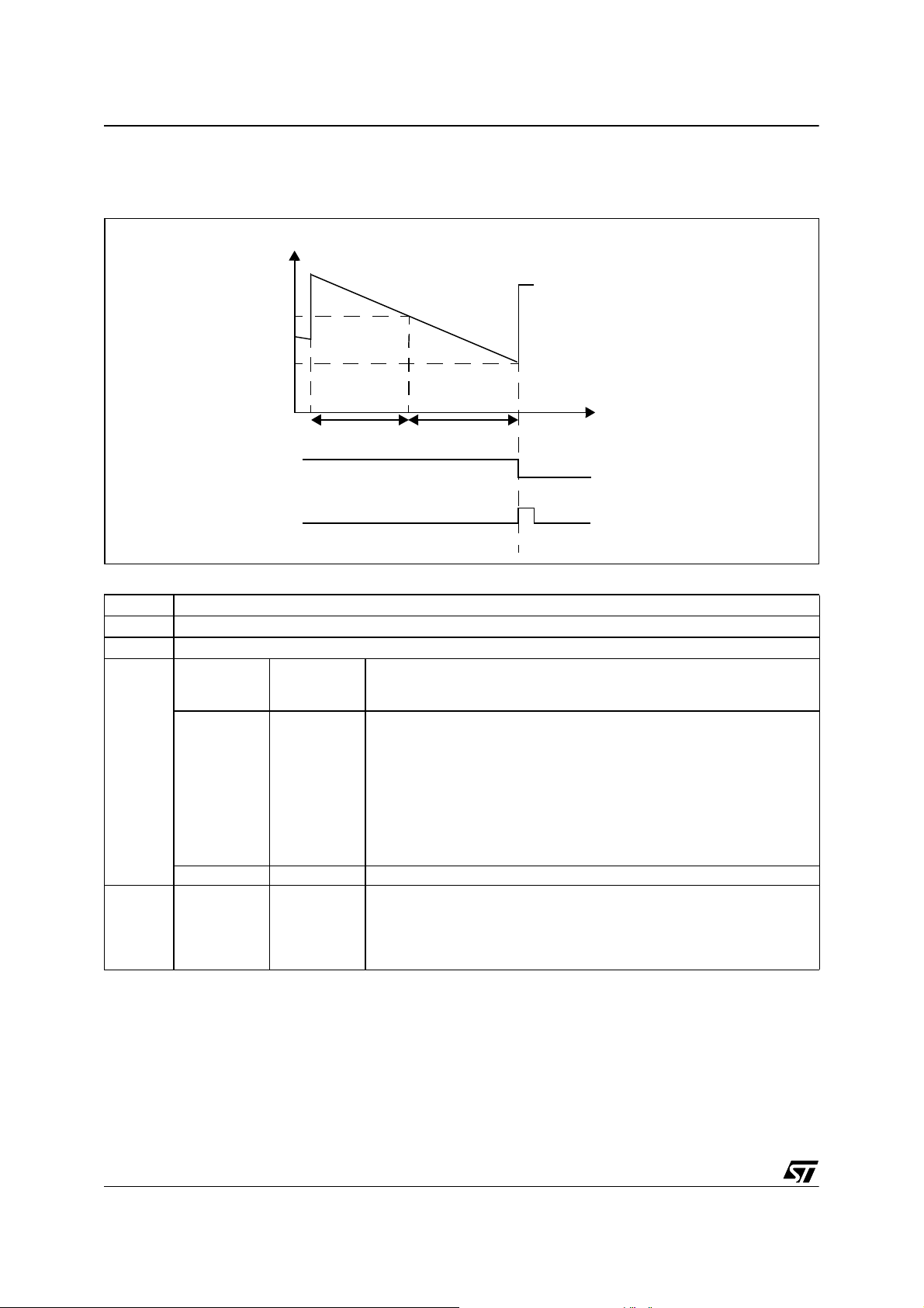
ST72561
WINDOW WATCHDOG (Cont’d)
Figure 37. Window Watchdog Timing Diagram
T[5:0] CNT downcounter
WDGWR
3Fh
Refresh WindowRefresh not allowed
T6 bit
Reset
time
(step = 16384/f
OSC2
)
10.1.6 Low Power Modes
Mode Description
SLOW No effect on Watchdog : the downcounter continues to decrement at normal speed.
WAIT No effect on Watchdog : the downcounter continues to decrement.
OIE bit in
MCCSR
register
HALT
00
0 1 A reset is generated instead of entering halt mode.
ACTIVE
HALT
1x
10.1.7 Hardware Watchdog Option
If Hardware Watchdog is selected by option b yte,
the watchdog is always active and the WDGA bit in
the WDGCR is not used. Refer to the Option By te
description.
WDGHALT bit
in Option
Byte
No Watchdog reset is generated. The MCU enters Halt mode. The Watchdog counter is decremented once and then stops counting and is no longer
able to generate a watchdog reset until the MCU receives an external interrupt or a reset.
If an interrupt is received (refer to interrupt table mapping to see interrupts
which can occur in halt mode), the Watchdog restarts counting after 256 or
4096 CPU clocks. If a reset is generated, the Watchdog is disabled (reset
state) unless Hardware Watchdog is selected by option byte. For application recommendations see Section 10.1.8 below.
No reset is generated. The MCU enters Active Halt mode. The Watchdog
counter is not decremented. It stop counting. When the MCU receives an
oscillator interrupt or external interrupt, the Watchdog restarts counting immediately. When the MCU receives a reset the Watchdog restarts counting
after 256 or 4096 CPU clocks.
10.1.8 Using Halt Mode with the WDG
(WDGHALT option)
The following recommendation applies if Halt
mode is used when the watchdog is enabled.
– Before execut ing the HALT instruction, refresh
the WDG counter, to avoid an unexpected WDG
reset immediately after waking up the microcontroller.
58/262
Page 59
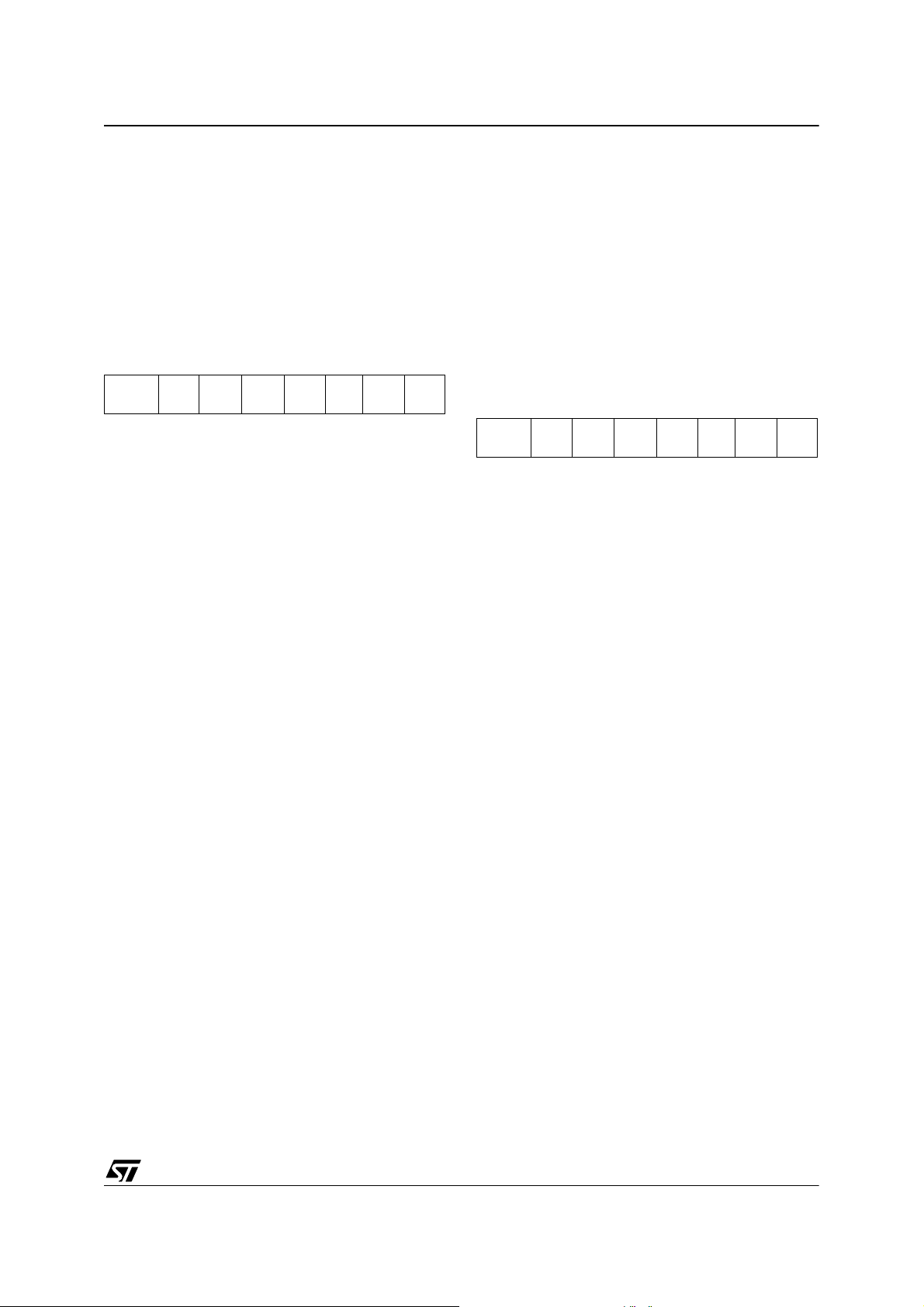
WINDOW WATCHDOG (Cont’d)
10.1.9 Interrupts
None.
Bits 6:0 = T[6:0] 7-bit counter (MSB to LSB).
These bits contain the value of the watchdog
10.1.10 Register Description
CONTROL REGISTER (WDGCR)
counter. It is decremented every 16384 f
cles (approx.). A reset is produced when it rolls
over from 40h to 3Fh (T6 becomes cleared).
Read/Write
Reset Value: 0111 1111 (7Fh)
70
WINDOW REGISTER (WDGWR)
Read/Write
Reset Value: 0111 1111 (7Fh)
WDGA T6 T5 T4 T3 T2 T1 T0
70
ST72561
cy-
OSC2
Bit 7 = WDGA Activation bit.
This bit is set by software and only cleared by
hardware after a reset. When WDGA = 1, the
watchdog can generate a reset.
0: Watchdog disabled
1: Watchdog enabled
Note: T his bit is not used if the hardware wat ch-
dog option is enabled by option byte.
- W6W5W4W3W2W1W0
Bit 7 = Reserved
Bits 6:0 = W[6:0] 7-bit window value
These bits contain the window value to be com-
pared to the downcounter.
59/262
Page 60

ST72561
WATCHD OG TI M E R (Cont’d)
Figure 38. Watchdog Timer Register Map and Reset Value s
Address
(Hex.)
2F
30
Register
Label
WDGCR
Reset Value
WWDGR
Reset Value
7654 3210
WDGA
0
-
0
T6
1
W6
1
T5
1
W5
1
T4
1
W4
1
T3
1
W3
1
T2
1
W2
1
T1
1
W1
1
T0
1
W0
1
60/262
Page 61
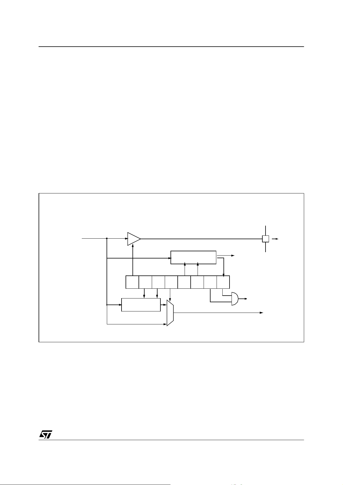
10.2 MAIN CLOCK CONTROLLER WITH REAL TIME CLOCK MCC/RTC
ST72561
The Main Clock Controller consi sts of three di fferent functions:
■
a programmable CPU clock prescaler
■
a clock-out signal to supply external devices
■
a real time clock timer with interrupt capability
Each function can be used independently and simultaneously.
10.2.1
Programmable CPU Clock Prescaler
The programmable CP U clock prescaler supplies
the clock for the ST7 CPU and its inte rnal peripherals. It manages SLOW power saving mode (See
Section 8.2 "SLOW MODE" for more details).
The prescale r select s th e f
main clock frequen-
CPU
cy and is controlled by three bits in the MCCSR
register : CP[1 :0 ] a n d SMS.
10.2.2
Clock- out Capabilit y
The clock-out capability is an alternate functio n of
an I/O port pin that outputs a f
external devices. It is controlled by t he M CO bit in
the MCCSR register.
10.2.3
Real Time Clo c k Ti m e r (R TC )
The counter of the real time clock t imer allows an
interrupt to be generated based on an accurate
real time clock. Four different time bases de pend-
ing directly on f
functionality is controlled by fo ur bits of the M CC-
SR register: TB[ 1 :0], OIE and OIF.
When the RTC interrupt is enabled (OIE bit set),
the ST7 enters ACTIVE-HALT mode when the
HALT instruction is executed. See Section 8.5
"ACTIVE-HALT MODE" for more details.
Figure 39. Main Clock Controller (MCC/RTC) Block Diagram
f
OSC2
cloc k to d rive
OSC2
are available. The whole
OSC2
MCO
MCO
MCCSR
DIV 2, 4, 8, 16
RTC
COUNTER
SMSCP1 CP0 TB1 TB0 OIE OIF
TO
WATCHDOG
TIMER
MCC/RTC INTERRUPT
f
CPU
CPU CLOCK
TO CPU AND
PERIPHERALS
61/262
Page 62
ST72561
MAIN CLOCK CONTROLLER WITH REAL TIME CLOCK (Cont’d)
10.2.4
10.2.5
The MCC/RTC interrupt even t generat es an interrupt if the OIE bit of the MCCSR register is set and
the interrupt mask in the CC register is not active
(RIM instruction).
Note:
The MCC/RTC interrupt wakes up the MCU from
ACTIVE-HALT mode, not from HALT or AWUF
HALT mode.
10.2.6
MCC CONTROL/STATUS REGISTER (MCCSR)
Read/Write
Reset Value: 0000 0000 (00h
Low Power Mo des
Mode Description
No effect on MCC/RTC peripheral.
WAIT
ACTIVEHALT
HALT
and
AWUF HALT
MCC/RTC interrupt cause the device to
exit from WAIT mode.
No effect on MCC/RTC counter (OIE bit
is set), the registers are frozen.
MCC/RTC interrupt cause the device to
exit from ACTIVE-HALT mode.
MCC/RTC counter and registers are
frozen.
MCC/RTC operation resumes when
the MCU is woken up by an interrupt
with “exit from HALT” capability.
Bit 6:5 = CP[1:0] CPU clock prescaler
These bits select the CPU clock prescaler which is
applied in the different slow modes. Their action is
conditioned by the setting of the SMS bit. These
two bits are set and cleared by software
f
in SLOW mode CP1 CP0
CPU
/ 2 0 0
f
OSC2
f
/ 4 0 1
OSC2
f
/ 8 1 0
OSC2
f
/ 16 1 1
OSC2
Bit 4 = SMS Slow mode select
Interrupts
This bit is set and cleared by software.
0: Normal mode. f
1: Slow mode. f
See Section 8.2 "SLOW MODE" and Section 10.2
= f
CPU
CPU
OSC2
is given by CP1, CP0
"MAIN CLOCK CONTROLLER WITH REAL TIME
CLOCK MCC/RTC" for more details.
Interrupt Event
Time base overflow
event
Register Description
Event
Enable
Control
Flag
OIF OIE Yes No
Bit
)
Exit
from
Wait
Exit
from
Halt
1)
Bit 3:2 = TB[1:0] Time base control
These bits select the programmable divider time
base. They are set and cleared by software.
Counter
Prescaler
16000 4ms 2ms 0 0
32000 8ms 4ms 0 1
80000 20ms 10ms 1 0
200000 50ms 25ms 1 1
f
OSC2
Time Base
=4MHz f
OSC2
A mod ificatio n of th e time bas e is taken into ac -
count at the end of the current period (previously
70
set) to avoid an unwanted time shift. This allows to
use this time base as a real time clock.
=8MHz
TB1 TB0
MCO CP1 CP0 SMS TB1 TB0 OIE OIF
Bit 7 = MCO Main clock out selection
This bit enables the MCO alternate function on the
corresponding I/O port. It is set and cleared by
software.
0: MCO alternate function disabled (I/O pin free for
general-purpose I/O)
1: MCO alternate function enabled (f
OSC2
on I/O
port)
62/262
Bit 1 = OIE Oscillator interrupt enable
This bit set and cleared by software.
0: Oscillator interrupt disabled
1: Oscillator interrupt enabled
This interrupt can be used to e xit from ACTIVE-
HALT mode.
When this bit is set, calling the ST7 software HALT
instruction enters the ACTIVE-HALT power saving
.
mode
Page 63
MAIN CLOCK CONTROLLER WITH REAL TIME CLOCK (Cont’d)
Bit 0 = OIF Oscilla t or in t er ru p t fl ag
This bit is set by hardware and cleared by software
reading the CSR register. It indicates when set
CAUTION: The BRES and BSET instructions
must not be used on the MCCSR register to avoid
unintentionally clearing the OIF bit.
that the main osc illator has reached t he selected
elapsed time (TB1:0).
0: Timeout not reached
1: Timeout reached
Table 15. Main Clock Controller Register Ma p and Reset Values
ST72561
Address
(Hex.)
002Dh
002Eh
Register
Label
SICSR
Reset Value
MCCSR
Reset Value
76543210
0 AVDIE AVDF LVDRF 0
MCO
0
CP1
0
CP0
0
SMS
0
TB1
0
00
TB0
0
OIE
0
WDGRF
x
OIF
0
63/262
Page 64
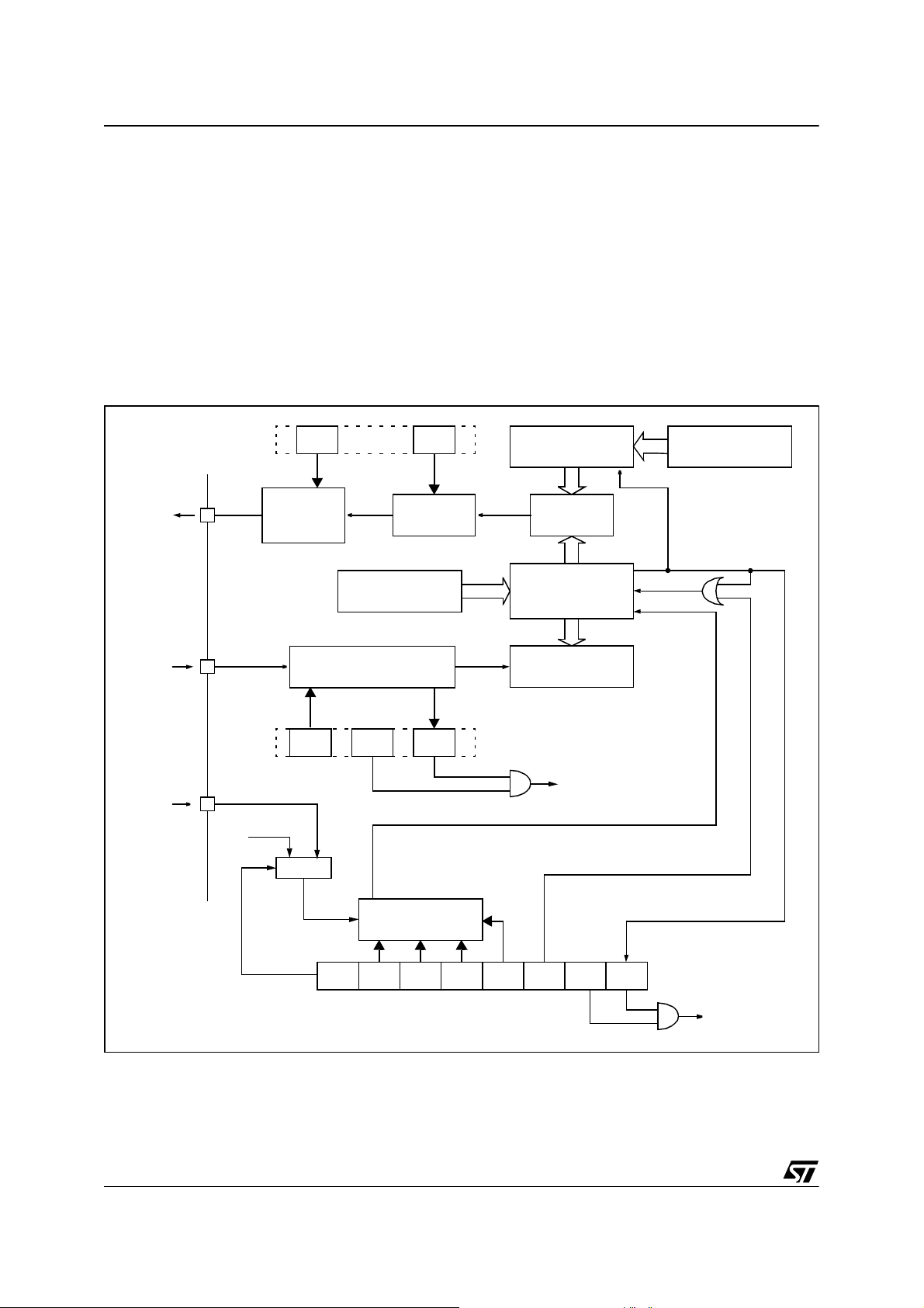
ST72561
10.3 PWM AUTO-RELOAD TIMER (ART)
10.3.1 Introduction
The Pulse Width Modulated Auto-Reload Timer
on-chip peripheral consists of an 8-bit auto reload
counter with compare/capture capabilities and of a
7-bit prescal er clock source.
These resources allow five possible operating
modes:
– Generation of up to 4 independent PWM signals
– Output compare and Time bas e interrupt
Figure 40. PWM Auto-Reload Timer Block Diagram
– Up to two input capture functions
– External event dete ctor
– Up to two external interrupt sources
The three first modes can be used together with a
single counter frequency.
The timer can b e used t o wake up the MCU from
WAIT and HALT modes.
PWMx
ARTICx
ARTCLK
PWMCR
ALTERNATE
FUNCTION
f
EXT
f
CPU
OEx
PORT
INPUT CAPTURE
MUX
ARR
REGISTER
CONTROL
ICIEx
OPx
POLARITY
CONTROL
ICFxICSx
f
COUNTER
LOAD
ICCSR
OCRx
REGISTER
COMPARE
8-BIT COUNTER
(CAR REGISTER)
ICRx
REGISTER
ICx INTERRUPT
DCRx
REGISTER
LOAD
LOAD
64/262
f
INPUT
EXCL CC2 CC1 CC0 TCE FCRL OIE OVF
PROGRAMMABLE
PRESCALER
ARTCSR
OVFINTERRUPT
Page 65
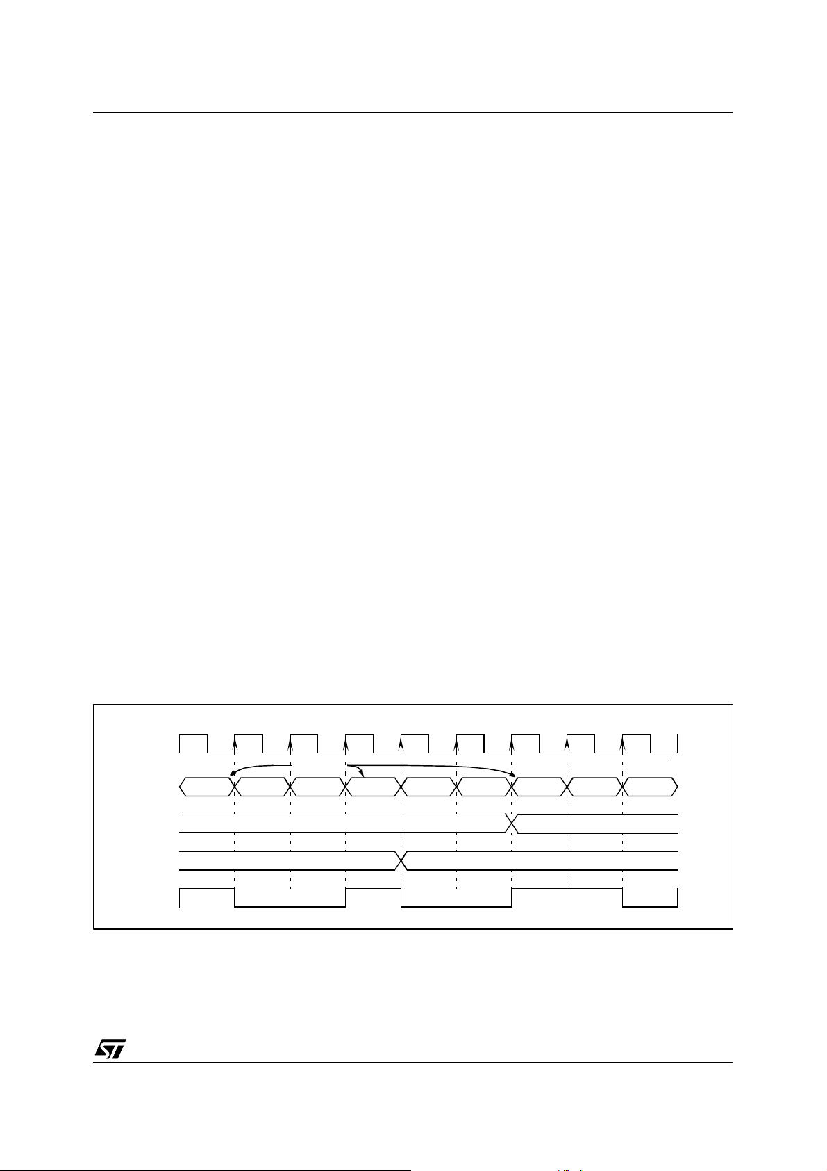
PWM AUTO-RELOAD TIMER (Cont’d)
10.3.2 Functional Description
ST72561
Counter
The free running 8-bit cou nter is fed by the output
of the prescaler, and is incremented on every rising edge of the clock signal.
It is possible to read or write the cont ents of the
counter on the fly by reading or writing the Counter
Access register (ARTCAR).
When a counter overflow occurs, the counter is
automatically reloaded with the contents of the
ARTARR register (the prescaler is not affected).
Counter clock and prescaler
The counter clock frequency is given by:
f
COUNTER
= f
INPUT
The timer counter’s input clock (f
/ 2
CC[2:0]
INPUT
) feeds the
7-bit programmable prescaler, which sel ects one
of the 8 available taps of the prescaler, as defined
by CC[2:0] bits in the Control/Status Register
(ARTCSR). Thus the division factor of the prescaler can be set to 2
This f
INPUT
n
(where n = 0, 1,..7).
frequency source is selected through
the EXCL bit of the ARTCSR register and can be
either the f
or an external input frequency f
CPU
EXT
The clock input to the counter is enabled by the
TCE (Timer Counter Enable) bit in the ARTCSR
register. When TCE is reset, the counter is
stopped and the prescaler and counter contents
are frozen. When T CE is set, the coun ter runs at
the rate of the selected clock sou rce .
Counter and Prescaler Initialization
After RESET, the counter and the prescaler are
cleared and f
INPUT
= f
CPU
.
The counter can be initialized by:
– Writing to the ARTARR register and then setting
the FCRL (Force Counter Re-Load) and the TCE
(Timer Counter Enable) bits in the ARTCSR reg-
ister.
– Writing to the ARTCAR counter access register,
In both cases the 7-b it prescaler is also cleared,
whereupon counting will start from a known value.
Direct access to the prescaler is not possible.
Output compare contro l
The timer compare function is based on four different comparisons with the counter (one for each
PWMx output). Each comparison is made between the counter value and an outpu t compare
register (OCRx) value. This OCRx register can not
be accessed directly, it is loaded from the duty cycle register (PWMDCRx) at each overflow of the
counter.
.
This double buffering method avoids glitch generation when changing the duty cycle on the fly.
Figure 41. Output compare control
f
COUNTER
ARTARR=FDh
COUNTER
OCRx
PWMDCRx
PWMx
FDh FEh FFh FDh FEh FFh FDh FEh
FDh
FDh
FFh
FEh
FEh
65/262
Page 66
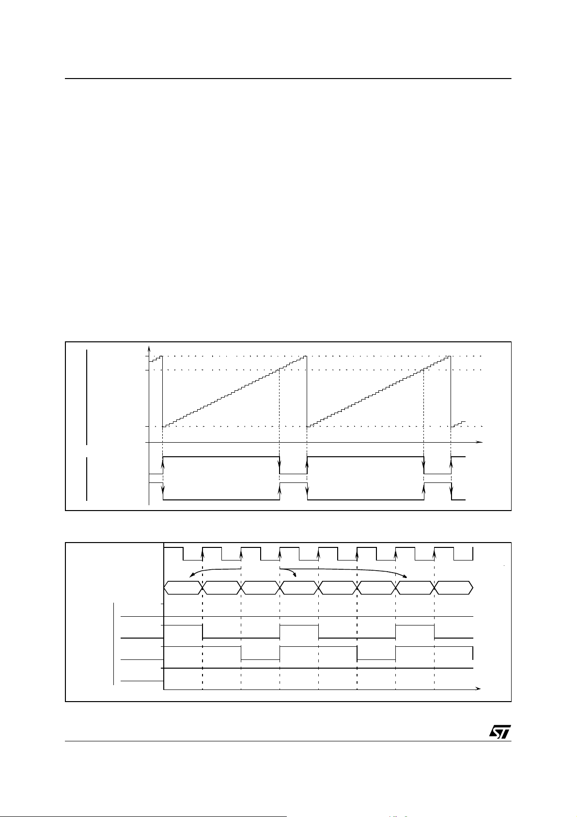
ST72561
PWM AUTO-RELOAD TIMER (Cont’d)
Independent PWM signal generation
This mode allows up to four Pulse Width Mo dulated signals to be generated on the PWMx output
pins with minimum core processing overhead.
This function is stopped during HALT mode.
Each PWMx ou tput signal can be selected independently using the corresponding OEx bit in the
PWM Control register (PWMCR). When this bit is
set, the corresponding I/O pin is configured as output push-pull alternate function.
The PWM signals all have the same frequency
which is controlled by the counter period and the
ARTARR register value.
f
PWM
= f
COUNTER
/ (256 - ARTARR)
When a counter overflow occurs, the PWMx pin
level is changed depending on the corresponding
OPx (output polarity) bit in the P WMCR register.
Figure 42. PW M Au to- re l oad Timer Fun ct io n
255
DUTY CYCLE
REGISTER
(PWMDCRx)
When the counter reaches the value contained in
one of the output compare register (OCRx) the
corresponding PWMx pin level is restored.
It should be noted that the reload values will also
affect the value and the resolution of t he duty cycl e
of the PWM output s ign al. T o obt ain a signal on a
PWMx pin, the contents of the OCRx register must
be greater than the con tents of the A RTARR register.
The maximum avai lable resolution for the PW Mx
duty cycle is:
Resolution = 1 / (256 - ARTARR)
Note: To get the maximum resolution (1/256), the
ARTARR register must be 0. With this maximum
resolution, 0% and 100% can be obtained by
changing the polarity.
AUTO-RELOAD
COUNTER
REGISTER
(ARTARR)
000
WITH OEx=1
AND OPx=0
WITH OEx=1
AND OPx=1
PWMx OUTPUT
Figure 43. PWM Signal from 0% to 100% Duty Cycle
f
COUNTER
ARTARR=FDh
COUNTER
OCRx=FCh
OCRx=FDh
OCRx=FEh
AND OPx=0
WITH OEx=1
PWMx OUTPUT
OCRx=FFh
FDh FEh FFh FDh FEh FFh FDh FEh
t
66/262
t
Page 67
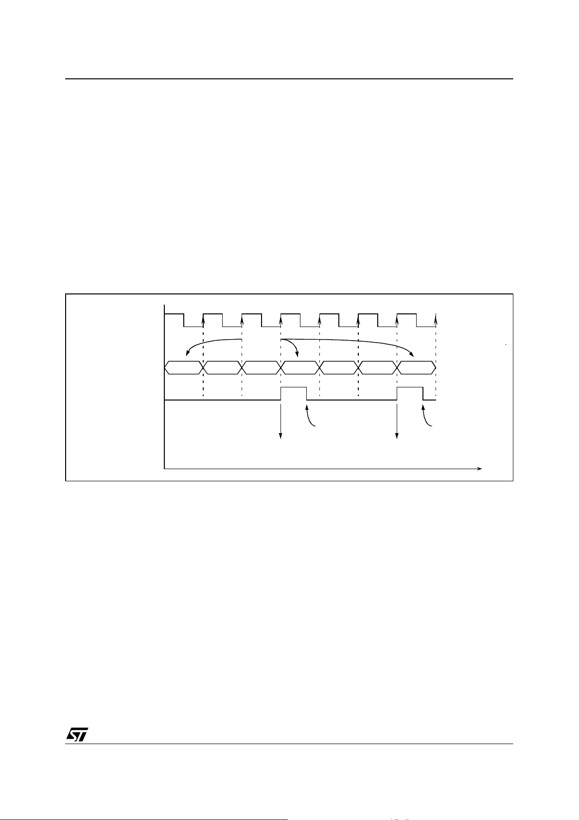
PWM AUTO-RELOAD TIMER (Cont’d)
ST72561
Output compare and Time base interru pt
On overflow, the OVF flag of the ARTCSR register
is set and an overflow interrupt request is generated if the overflow interrupt enable bit, OIE, in the
ARTCSR register, is set. The OVF flag must be reset by the user software. This interrupt can be
External clock and event detector mode
Using the f
auto-reload timer can be used as an external clock
event detector. In this mode, the ARTARR register
is used to select the n
be counted before setting the OVF flag.
used as a time base in the application.
Caution: The external clock function is not available in HALT mode. If HALT mode is used in the application, prior to executing the HALT instruction,
the counter must b e di sa bled by clea ring the TCE
bit in the ARTCSR register to avoid spurious counter increments.
Figure 44. External Event Detector Example (3 counts)
f
EXT=fCOUNTER
ARTARR=FDh
COUNTER
OVF
FDh FEh FFh FDh
external prescaler input clock, the
EXT
EVENT
n
FEh FFh FDh
= 256 - ARTARR
EVENT
number of even ts to
INTERRUPT
IF OIE=1
ARTCSR READ
ARTCSR READ
INTERRUPT
IF OIE=1
t
67/262
Page 68
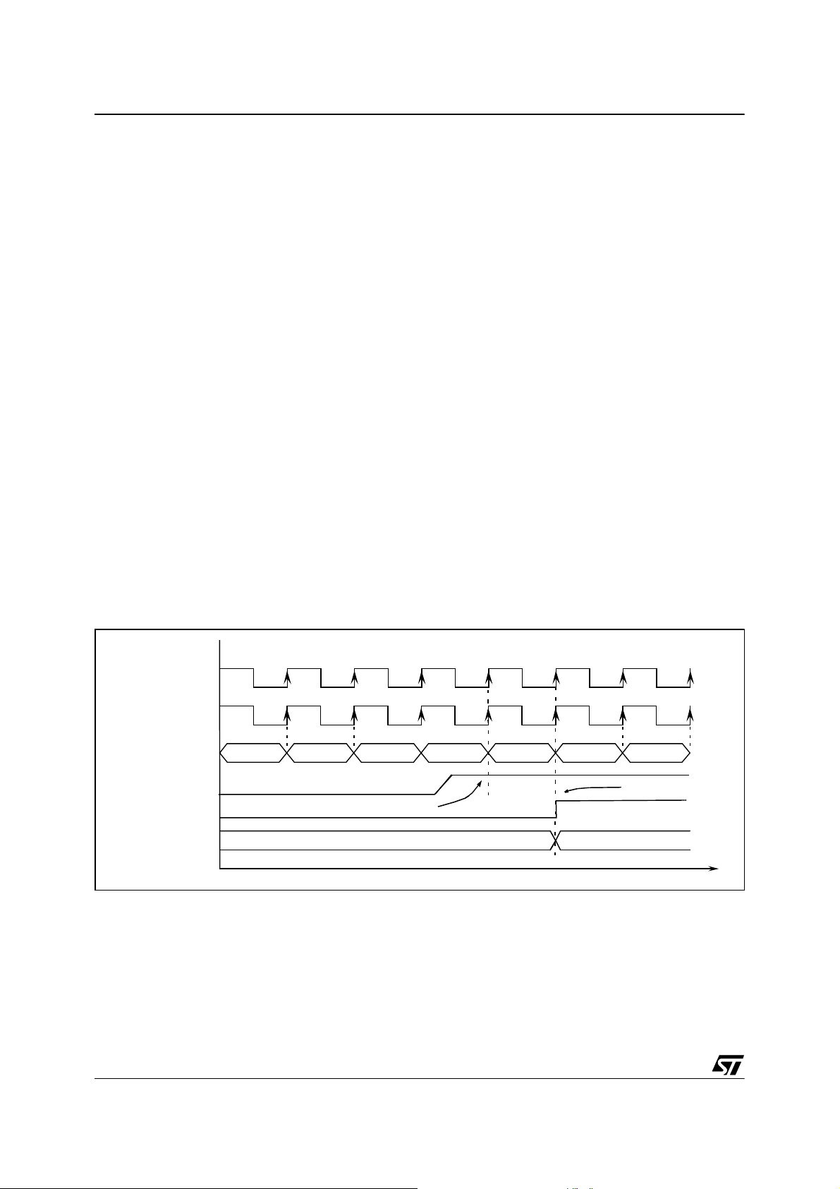
ST72561
PWM AUTO-RELOAD TIMER (Cont’d)
Input Capt ure Function
Input Capture mode allows the measurement of
external signal pulse widths through ARTICRx
registers.
Each input capture can generate an interrupt independently on a selected input signal transition.
This event is flagged by a set of the corresponding
CFx bits of the Input Capture Control/Status register (ARTICCSR).
These input capture interrupts are enabled
through the CIEx bits of the ARTICCSR register.
The active transition (falling or rising edge) is software programmable through the CSx bits of the
ARTICCSR register.
The read only input capture registers (ARTICRx)
are used to latch the auto-reload counter value
when a transition is detected on the ARTICx pin
(CFx bit set in ARTICCSR register). After fetching
the interrupt vector, the CFx flags can be read t o
identify the interrupt source.
Note: After a capture detection, data transfer in
the ARTICRx register is inhibited until the next
read (clearing the CFx bit).
The timer interrupt remains pending while the CFx
flag is set when the interrupt is enabled (CIEx bit
set). This means, the ARTICRx register has to be
read at each capture event to clear the CFx flag.
The timing resolution is given by auto-reload counter cycle time (1/f
COUNTER
).
Note: During HALT mode, i nput capt ure is i nhibited (the ARTICRx is never re-load ed) and only t he
external interrupt capability can be used.
Note: The ARTICx signal is synchronized on CPU
clock. It takes two rising edges un til ARTICRx is
latched with the counter value. Depending on the
prescaler value and the time when the ICAP event
occurs, the value loaded in the ARTICRx register
may be different.
If the counter is clocked with the CPU clock, the
value latched in ARTICRx is always the next counter value after the event on ARTICx occurred (Fig-
ure 45).
If the counter clock is prescaled, it depends on the
position of the ARTICx event within the counter cycle (Figure 46).
Figure 45. Input Capture Timing Diagram, f
f
CPU
f
COUNTER
COUNTER
ARTICx PIN
CFx FLAG
ICAP SAMPLED
01h
02h 03h 05h 06h 07h
ICAP SAMPLED
xxh
counter
= f
cpu
04h
.
INTERRUPT
05h
t
68/262
Page 69
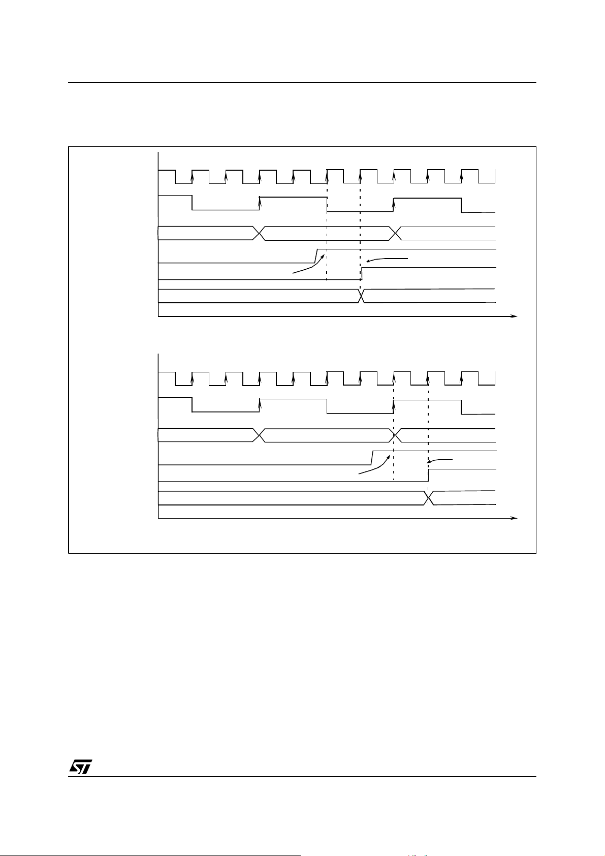
PWM AUTO-RELOAD TIMER (Cont’d)
ST72561
Figure 46. input Capture Timing Diagram, f
f
CPU
f
COUNTER
COUNTER
ARTICx PIN
CFx FLAG
ICRx REGISTER
f
CPU
f
COUNTER
COUNTER
03h
ICAP SAMPLED
xxh
03h
COUNTER
= f
04h
04h
cpu
/ 4.
05h
INTERRUPT
04h
t
05h
ARTICx PIN
CFx FLAG
ICRx REGISTER
xxh
INTERRUPT
ICAP SAMPLED
05h
t
69/262
Page 70

ST72561
External Interrup t Ca pab ility
This mode allows th e Input captur e capabilit ies to
be used as external interrupt sources . The interrupts are generated on the edge of the ARTICx
signal.
The edge sensitivity of the external interrupts is
programmable (CSx bit of ARTICCSR register)
and they are independently enabled through CIEx
bits of the ARTICCSR register. After fetching the
interrupt vector, the CFx flags can be read to identify the interrupt source.
During HALT mode, the external interrupts can be
used to wake up the micro (if the CIEx bit is set). In
this case, the interrupt synchronization is done directly on the ARTICx pin edge (Figure 47).
Figure 47. ART External Interrupt in HALT
mode
ARTICx PIN
CFx FLAG
INTERRUPT
t
70/262
Page 71
PWM AUTO-RELOAD TIMER (Cont’d)
10.3.3 Register Description
ST72561
CONTROL / STATUS REGISTER (ARTCSR)
Read/Write
Reset Value: 0000 0000 (00h)
70
0: New transition not yet reached
1: Transition reached
COUNTER ACCESS REGISTER (ARTCAR)
Read/Write
Reset Value: 0000 0000 (00h)
EXCL CC2 CC1 CC0 TCE FCRL OIE OVF
Bit 7 = EXCL
External Clock
70
CA7CA6CA5CA4CA3CA2CA1CA0
This bit is set and cleared by software. I t selects the
input clock for the 7-bit prescaler.
0: CPU clock.
1: External clock.
Bit 6:4 = CC[2:0] Counter Clock Control
These bits are set and cleared by software. They
determine the prescaler division ratio from f
f
COUNTER
f
INPUT
f
INPUT
f
INPUT
f
INPUT
f
INPUT
f
INPUT
f
INPUT
f
INPUT
/ 2
/ 4
/ 8
/ 16
/ 32
/ 64
/ 128
With f
=8 MHz CC2 CC1 CC0
INPUT
8 MHz
4 MHz
2 MHz
1 MHz
500 KHz
250 KHz
125 KHz
62.5 KHz
0
0
0
0
1
1
1
1
0
0
1
1
0
0
1
1
INPUT
0
1
0
1
0
1
0
1
Bit 7:0 = CA[7:0] Counter Access Data
These bits can be set and cleared either by hard-
ware or by software. The ARTCAR register is used
to read or write the auto-reload counter “on the fly”
(while it is counting).
.
AUTO-RELOAD REGISTER (ARTARR)
Read/Write
Reset Value: 0000 0000 (00h)
70
AR7AR6AR5AR4AR3AR2AR1AR0
Bit 3 = TCE Timer Counter Enable
This bit is set and cleared by s oftware. It puts the
timer in the lowest power consumption mode.
0: Counter stopped (prescaler and counter frozen).
1: Counter running.
Bit 2 = F CRL
Force Counter Re-Load
This bit is write-only and any attempt to read it will
yield a logical zero. When set, it causes the contents
of ARTARR register to be loaded into the counter,
and the content of the prescaler register to be
cleared in order to initialize the timer before starting
to count.
Bit 1 = OIE
Overflow Interrupt Enable
This bit is set and cleared by software. It allows to
enable/disable the interrupt which is generated
when the OVF bit is set.
0: Overflow Interrupt disable.
1: Overflow Interrupt enable.
Bit 0 = OVF
Overflow Flag
This bit is set by hardware and cleared by software
reading the ARTCSR register. It indicates the transition of the counter from FFh to the ARTARR val-
.
ue
Bit 7:0 = AR[7:0]
Counter Auto-Reload Data
These bits are set and cleared by software. They
are used to hold the auto-reload value which is automatically loaded in the counter when an overflow
occurs. At the same tim e, the PWM output levels
are changed according to the corresponding OPx
bit in the PWMCR register.
This register has two PWM management functions:
– Adjusting the PWM frequency
– Setting the PWM duty cycle resolution
PWM Frequency vs. Resolution:
f
ARTARR
value
0 8-bit ~0.244-KHz 31.25-KHz
[ 0..127 ] > 7-bit ~0.244-KHz 62.5-KHz
[ 128..191 ] > 6-bit ~0.488-KHz 125-KHz
[ 192..223 ] > 5-bit ~0.977-KHz 250-KHz
[ 224..239 ] > 4-bit ~1.953-KHz 500-KHz
Resolution
PWM
Min Max
71/262
Page 72
ST72561
PWM AUTO-RELOAD TIMER (Cont’d)
PWM CONTROL REGISTER (PWMCR)
Read/Write
Reset Value: 0000 0000 (00h)
70
OE3 OE2 OE1 OE0 OP3 OP2 OP1 OP0
Bit 7:4 = OE[3:0] PWM Output Enable
These bits are set and cleared by software. They
enable or disable the PWM output ch annels independently acting on the corresponding I/O pin.
0: PWM output disabled.
1: PWM output enabled.
Bit 3:0 = OP[3:0] PWM Output Polarity
These bits are set and cleared by software. They
independently select the po larity of the four PW M
DUTY CYCLE REGISTERS (PWMDCRx)
Read/Write
Reset Value: 0000 0000 (00h)
70
DC7 DC6 DC5 DC4 DC3 DC2 DC1 DC0
Bit 7:0 = DC[7:0] Duty Cycle Data
These bits are set and cleared by software.
A PWMDCRx register is associated with the OCRx
register of each PWM channel to determine the
second edge location of the PWM signal (the first
edge location is common to all channels and given
by the ARTARR register). These PWMDCR registers allow the duty cycle to be set independently
for each PWM channel.
output signals.
PWMx output level
Counter <= OCRx Counter > OCRx
100
011
OPx
Note: When an OPx bit is modified, the PWMx out-
put signal polarity is immediately reversed.
72/262
Page 73

PWM AUTO-RELOAD TIMER (Cont’d)
ST72561
INPUT CAPTURE
CONTROL / STATUS REGISTER (ARTICCSR)
Read/Write
INPUT CAPTURE REGISTERS (ARTICRx)
Read only
Reset Value: 0000 0000 (00h)
Reset Value: 0000 0000 (00h)
70
70
IC7IC6IC5IC4IC3IC2IC1IC0
0 0 CS2 CS1 CIE2 CIE1 CF2 CF1
Bit 7:0 = IC[7:0] Input Capture Data
Bit 7:6 = Reserved, always read as 0.
These read only bits are set and cleared by hard-
ware. An ARTICRx register contains the 8-bit
Bit 5:4 = CS[2:1] Capture Sensitivity
These bits are set and cleared by software. They
auto-reload counter v alue trans ferre d b y the input
capture channel x event.
determine the trigger event polarity on the corresponding input capture channel.
0: Falling edge triggers capture on channel x.
1: Rising edge triggers capture on channel x.
Bit 3:2 = CIE[2:1] Capture Interrupt Enable
These bits are set and cleared by software. They
enable or disable the Input capture channel interrupts independently.
0: Input capture channel x interrupt disabled.
1: Input capture channel x interrupt enabled.
Bit 1:0 = CF[2:1] Capture Flag
These bits are set by hardware and cleared by
software reading the corresponding ARTICRx register. Each CFx bit indicates that an input capture x
has occurred.
0: No input capture on channel x.
1: An input capture has occured on channel x.
73/262
Page 74

ST72561
PWM AUTO-RELOAD TIMER (Cont’d)
Table 16. PWM Auto-Reload Timer Register Map and Reset Values
Address
(Hex.)
0031h
0032h
0033h
0034h
0035h
0036h
0037h
0038h
0039h
003Ah
Register
Label
PWMDCR3
Reset Value
PWMDCR2
Reset Value
PWMDCR1
Reset Value
PWMDCR0
Reset Value
PWMCR
Reset Value
ARTCSR
Reset Value
ARTCAR
Reset Value
ARTARR
Reset Value
ARTICCSR
Reset Value
ARTICR1
Reset Value
76543210
DC7
0
DC7
0
DC7
0
DC7
0
OE3
0
EXCL
0
CA7
0
AR7
0
00
IC7
0
DC6
0
DC6
0
DC6
0
DC6
0
OE2
0
CC2
0
CA6
0
AR6
0
IC6
0
DC5
0
DC5
0
DC5
0
DC5
0
OE1
0
CC1
0
CA5
0
AR5
0
CE2
0
IC5
0
DC4
0
DC4
0
DC4
0
DC4
0
OE0
0
CC0
0
CA4
0
AR4
0
CE1
0
IC4
0
DC3
0
DC3
0
DC3
0
DC3
0
OP3
0
TCE
0
CA3
0
AR3
0
CS2
0
IC3
0
DC2
0
DC2
0
DC2
0
DC2
0
OP2
0
FCRL
0
CA2
0
AR2
0
CS1
0
IC2
0
DC1
0
DC1
0
DC1
0
DC1
0
OP1
0
RIE
0
CA1
0
AR1
0
CF2
0
IC1
0
DC0
0
DC0
0
DC0
0
DC0
0
OP0
0
OVF
0
CA0
0
AR0
0
CF1
0
IC0
0
003Bh
74/262
ARTICR2
Reset Value
IC7
0
IC6
0
IC5
0
IC4
0
IC3
0
IC2
0
IC1
0
IC0
0
Page 75

10.4 16-BIT TIMER
ST72561
10.4.1 Introduction
The timer consists of a 16-bit free-running counter
driven by a programmable prescaler.
It may be used for a variety of purposes, including
pulse length measurement of up to two input signals (input capture) or generation of up to two out-
put waveforms (output compare and PWM).
Pulse lengths and waveform perio ds can be modulated from a few microseconds to several milliseconds using the timer prescaler and the CPU
clock prescaler.
Some ST7 devices have two on-chip 16-bit timers.
They are completely independent, and do not
share any resources. They are synchronized a fter
a MCU reset as long as the timer clock frequencies are not modified.
This description covers one or two 16-bit timers. In
ST7 devices with two timers, register na mes are
prefixed with TA (Timer A) or TB (Timer B).
10.4.2 Main Features
■ Programmable prescaler: f
■ Overflow status flag and maskable interrupt
■ External clock input (must be at least 4 times
slower than the CPU
clock speed) with the choice
divided by 2, 4 or 8.
CPU
of active edge
■ 1 or 2 Output Compare functions each with:
– 2 dedicated 16-bit registers
– 2 dedicated programmable signals
– 2 dedicated status flags
– 1 dedicated maskable interrupt
■ 1 or 2 Input Capture functions each with:
– 2 dedicated 16-bit registers
– 2 dedicated active edge selection signals
– 2 dedicated status flags
– 1 dedicated maskable interrupt
■ Pulse width modulation mode (PWM)
■ One pulse mode
■ Reduced Power Mode
■ 5 alternate functions on I/O ports (ICAP1, ICAP2,
OCMP1, OCMP2, EXTCLK)*
When reading an input signal on a non-bonded
pin, the value will always be ‘1’.
10.4.3 Functional Description
10.4.3.1 Counter
The main block of the Programmable Timer is a
16-bit free running upcounter and its associated
16-bit registers. The 16-bit registers are made up
of two 8-bit registers called high & low.
Counter Register (CR):
– Counter High Register (CHR) is the most sig-
nific a nt byte ( MS By te ) .
– Counter Low Register (CLR) is the least sig-
nificant byte (LS Byte).
Alternate Counter Register (ACR)
– Alternate Counter H igh Re gist er (ACH R) is the
most significant byte (MS Byte).
– Alternate Counter Low Register (ACLR) is the
least significant byte (LS Byte).
These two read-only 16-bit registers contain the
same value but with the difference that reading the
ACLR register does not clear the TOF bit (Timer
overflow flag), located in the Status register, (SR),
(see note at the end of paragraph titled 16-bit read
sequence).
Writing in the CLR register or ACLR register resets
the free running counter to the FFFCh value.
Both counters have a reset value of FFFCh (this is
the only value which is reloaded in the 16-bit tim-
er). The reset value of both counters is also
FFFCh in One Pulse mode and PWM mode.
The timer clock depends on the clock con trol bits
of the CR2 register, as illustrated in Table 17 Clock
Control Bits. The value in the c ounter register re-
peats every 131072, 262144 or 524288 CPU clock
cycles depending on the CC[1:0] bits.
The timer frequency can be f
CPU
/2, f
CPU
/4, f
CPU
/8
or an external frequency.
The Block Diagram is shown in Figure 48.
*Note: So me time r pin s m ay not be available (not
bonded) in some ST7 devices. Refer to the device
pin out description.
75/262
Page 76
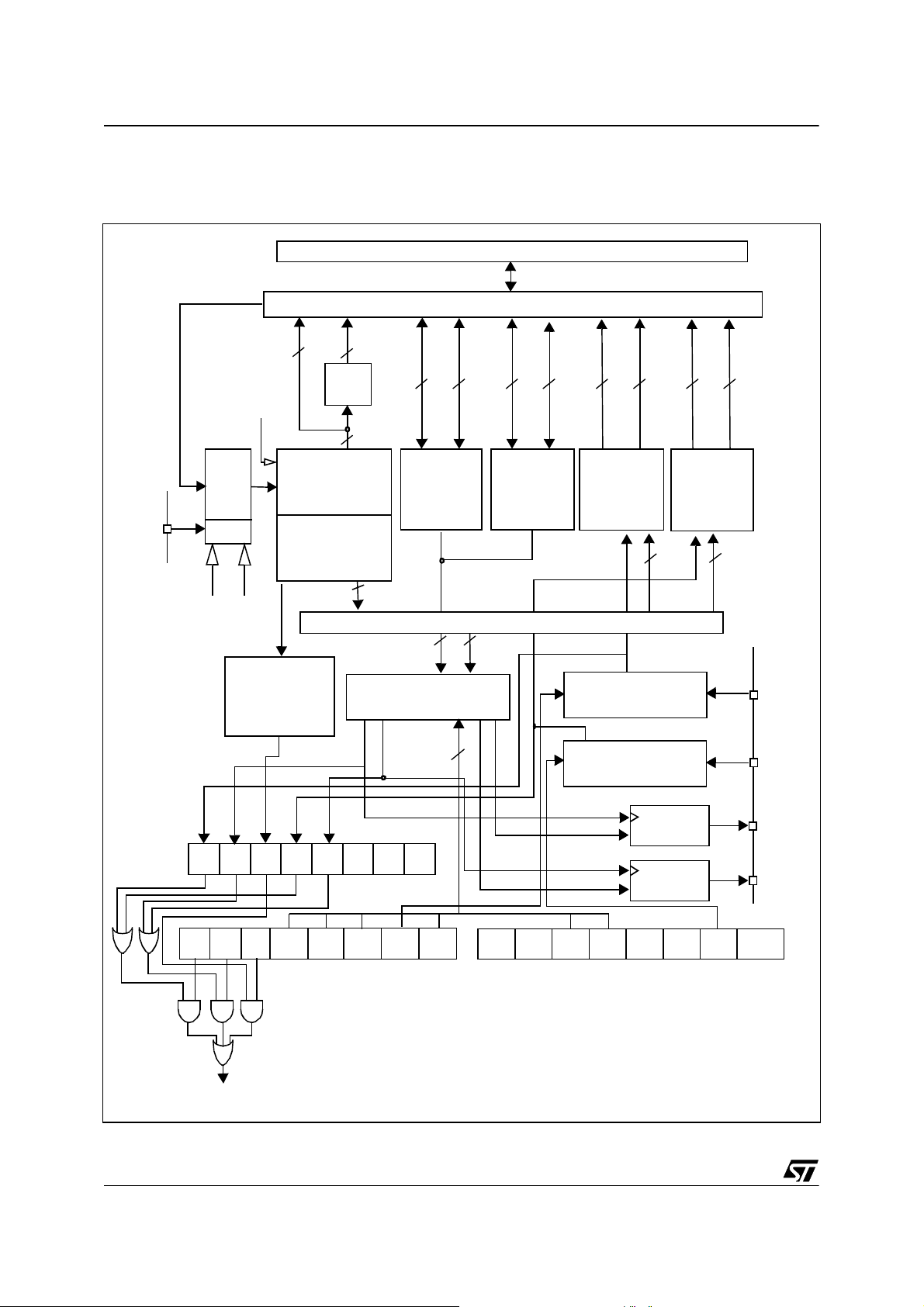
ST72561
16-BIT TIMER (Cont’d)
Figure 48. Tim er B l ock Di a gra m
f
CPU
ST7 INTERNAL BUS
MCU-PERIPHERAL INTERFACE
EXTCLK
pin
EXEDG
1/2
1/4
1/8
CC[1:0]
8 high
COUNTER
REGISTER
ALTERNATE
COUNTER
REGISTER
OVERFLOW
DETECT
CIRCUIT
8 low
8-bit
buffer
high
16
OUTPUT
COMPARE
REGISTER
16
TIMER INTERNAL BUS
OUTPUT COMPARE
CIRCUIT
low
1
16 16
6
8
high
low
OUTPUT
COMPARE
REGISTER
2
88 8
high
INPUT
CAPTURE
REGISTER
EDGE DETECT
CIRCUIT1
EDGE DETECT
CIRCUIT2
8
8 8 8
low
1
16
high
low
INPUT
CAPTURE
REGISTER
2
16
ICAP1
pin
ICAP2
pin
76/262
(See note)
TIMER INTERRUPT
ICF2ICF1
OCF2OCF1 TOF
(Control/Status Register)
TIMD
0
CSR
(Control Register 1) CR1
LATCH1
0
LATCH2
OC2E
PWMOC1E
OPMFOLV2ICIE OLVL1IEDG1OLVL2FOLV1OCIE TOIE
IEDG2CC0CC1
(Control Register 2) CR2
Note: If IC, OC and TO interrupt requests have separate vectors
then the last O R is not presen t (See device Interrupt Vector Table)
OCMP1
pin
OCMP2
pin
EXEDG
Page 77
16-BIT TIMER (Cont’d)
16-bit read seque nce: (from either the Counter
Register or the Alternate Counter Register).
Beginning of the sequence
At t0
Read
MS Byte
LS Byte
is buffered
Other
instructions
Returns the buffered
LS Byte value at t0
At t0 +∆t
Read
LS Byte
Sequence completed
The user must read the MS Byt e first, then th e LS
Byte value is buffered automatically.
This buffered value rem ains unchanged until th e
16-bit read sequence is completed, even if the
user reads the MS Byte several times.
After a complete reading sequence, if only the
CLR register or ACLR register are read, they return the LS Byte of the count v alue at the time of
the read.
Whatever the timer mode used (input capture, output compare, one pulse mode or PWM mode) an
overflow occurs when the counter rolls over from
FFFFh to 0000h then:
– The TOF bit of the SR register is set.
– A timer interrupt is generated if:
– TOIE bit of the CR1 register is set and
– I bit of the CC register is cleared.
If one of these cond itions is false, the interrupt remains pending to be issued as soon as they are
both true.
ST72561
Clearing the overflow interrupt request is done in
two steps:
1.Reading the SR register while the TOF bit is set.
2.An access (read or write) to the CLR register.
Notes: The TOF bit is not cleared by accesses to
ACLR register. The advantage of accessing the
ACLR register rather than the CLR register is that
it allows simultaneous use of the overflow function
and reading the free running counter at random
times (for example, to measure elapsed time) without the risk of clearing the TOF bit erroneously.
The timer is not affected by WAIT mode.
In HALT mode, the counter stops counting until the
mode is exited. Counting then resumes from the
previous count (MCU awakened by an interrupt) or
from the reset count (MCU awakened by a Reset).
10.4.3.2 External Clock
The external clock (where av ailable) is select ed if
CC0=1 and CC1=1 in the CR2 register.
The status of the EXEDG bit in the CR2 register
determines the type of level transition on the external clock pin EXTCLK that will trigger the free running counter.
The counter is synchronize d with the falling edge
of the internal CPU clock.
A minimum of four falling edges of the CPU clock
must occur between two consecutive active edges
of the external clock; thus t he external clock frequency must be less than a quarter of the CPU
clock frequency.
77/262
Page 78
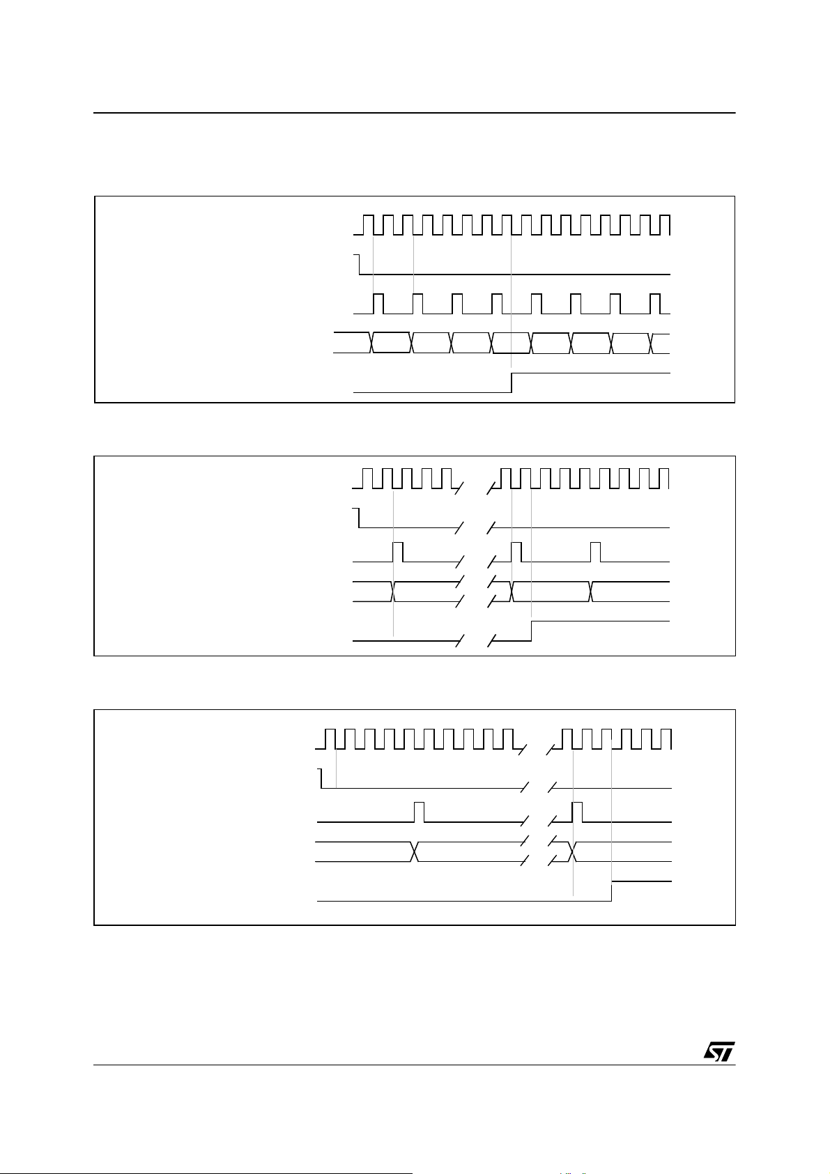
ST72561
16-BIT TIMER (Cont’d)
Figure 49. Counter Timing Diagram, internal clock divided by 2
CPU CLOCK
INTERNAL RESET
TIMER CLOCK
COUNTER REGISTER
TIMER OVERFLOW FLAG (TOF)
FFFD FFFE FFFF 0000 0001 0002 0003
Figure 50. Counter Timing Diagram, internal clock divided by 4
CPU CLOCK
INTERNAL RESET
TIMER CLOCK
COUNTER REGI STER
TIMER OVERFLOW FLAG (TOF)
FFFC FFFD 0000 0001
Figure 51. Counter Timing Diagram, internal clock divided by 8
CPU CLOCK
INTERNAL RESET
TIMER CLOCK
COUNTER REGISTER
TIMER OVERFLOW FLAG (TOF)
FFFC FFFD
0000
Note: The MCU is in reset state when the internal reset signal is high, when it is low the MCU is running.
78/262
Page 79

16-BIT TIMER (Cont’d)
10.4.3.3 Input Capture
In this section, the index, i, may be 1 or 2 because
there are 2 input capture functions in the 16-bit
timer.
The two 16-bit input capture registers (IC1R and
IC2R) are used to latch the valu e of the free running counter after a transition is detected on the
ICAPi pin (see figure 5).
MS Byte LS Byte
ICiR ICiHR ICiLR
ICiR register is a read-only register.
The active transition is software programmable
through the IEDGi bit of Control Registers (CRi).
Timing resolution is one count of the free running
f
counter: (
CPU
/CC[1:0]).
Procedure:
To use the input capture function select the following in the CR2 register:
– Select the timer clock (CC[1:0]) (see Table 17
Clock Control Bits).
– Select the edge of the active transition o n the
ICAP2 pin with the IEDG2 bit (the ICAP2 pin
must be configured as floating input or input with
pull-up without interrupt if this configuration is
available).
And select the following in the CR1 register:
– Set the IC IE b it to generat e an in terrupt after a n
input capture com ing from e ither the ICAP1 pin
or the ICAP2 pin
– Select the edge of the active transition o n the
ICAP1 pin with the IEDG1 bit (the ICAP1pin must
be configured as floating inp ut or inp ut with pul l-
up without interrupt if this configuration is availa-
ble).
ST72561
When an input capture occurs:
– IC Fi bit is set.
– Th e ICiR register contains the value of the free
running counter on the active transition on the
ICAPi pin (see Figure 53).
– A timer interrupt is generated if the ICIE bit is set
and the I bit is cleared in the CC register. Otherwise, the interrupt remains pending until both
conditions become true.
Clearing the Input Capture in terrupt request (i.e.
clearing the ICFi bit) is done in two steps:
1. Reading the SR register while the ICFi bit is set.
2. An access (read or write) to the ICiLR register.
Notes:
1. After reading the ICiHR register, transfer of
input capture data is inhibited and ICFi will
never be set until the ICiLR register is also
read.
2. The ICiR register contains the free running
counter value which corresponds to the most
recent input capture.
3. The 2 input capture functions can be used
together even if the timer also uses the 2 output
compare functions.
4. In One pulse Mode and PWM mode only Input
Capture 2 can be used.
5. The alternate inputs (ICAP1 & ICAP2) are
always directly connec ted to the timer. So any
transitions on these pins activates the input
capture function.
Moreover if one of the ICAPi pins is configured
as an input and t he second one as an output,
an interrupt can be generated if the user toggles the output pin and if the ICIE bit is set.
This can be avoided if the in put capture function i is disabled by reading the ICiHR (see note
1).
6. The TO F bit c an be used with interrupt generation in order to m easure events t hat go bey ond
the timer range (FFFFh).
79/262
Page 80
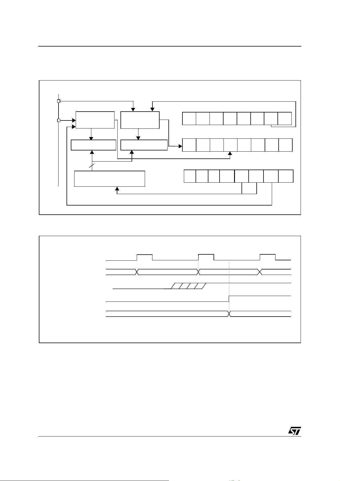
ST72561
16-BIT TIMER (Cont’d)
Figure 52. Input Capture Block Diagram
ICAP1
pin
ICAP2
pin
EDGE DETECT
CIRCUIT2
IC2R Register
16-BIT
16-BIT FREE RUNNING
COUNTER
EDGE DETECT
CIRCUIT1
IC1R Register
Figure 53. Input Capture Timing Diagram
TIMER CLOCK
ICIE
(Control Register 1) CR1
IEDG1
(Status Register) SR
ICF2ICF1 000
(Control Register 2) CR2
IEDG2
CC0
CC1
COUNTER REGISTER
ICAPi FLAG
ICAPi REGISTER
Note: The rising edge is the active edge.
80/262
FF01 FF02 FF03
ICAPi PIN
FF03
Page 81

16-BIT TIMER (Cont’d)
10.4.3.4 Output Compare
In this section, the index, i, may be 1 or 2 because
there are 2 output compare functions in the 16-bit
timer.
This function can be used to control an output
waveform or indicate when a period of time has
elapsed.
When a match is found bet ween the Out put Com pare register and the free running counter, the output compare function:
– Assigns pins with a programmable value if the
OCiE bit is set
– Sets a flag in the status register
– Generates an interrupt if enabled
Two 16-bit registers Output Compare Regist er 1
(OC1R) and Output Compare Register 2 (OC2R)
contain the value to be com pared to the counter
register each timer clock cycle.
MS Byte LS Byte
OCiROCiHR OCiLR
These registers are readable and writable and are
not affected by the timer hardware. A reset event
changes the OC
iR value to 8000h.
Timing resolution is one count of the free running
counter: (
f
CPU/
CC[1:0]
).
Procedure:
To use the output compare function, select the following in the CR2 register:
– Set the OCiE bit if an output is needed then the
OCMPi pin i s dedicated to the output com pare i
signal.
– Select the timer clock (CC[1:0]) (see Table 17
Clock Control Bits).
And select the following in the CR1 register:
– Select the OLVLi bit to applied to the OCMPi pins
after the match occurs.
– Set the OCIE bit to generate an interrupt i f it is
needed.
When a match is found between OCRi register
and CR register:
– OCFi bit is set.
ST72561
– The OCMP i pin take s OLVL i bit value (OCMPi
pin latch is forced low during reset).
– A timer interrupt is generated if the OCIE bit is
set in the CR1 register and the I bit is cleared in
the CC register (CC).
The OC
iR register value required for a specific tim-
ing application can be c alcul ated using the following f ormula:
∆t * f
∆ OCiR =
CPU
PRESC
Where:
∆t = Output compare period (in seconds)
f
= CPU clock frequency (in hertz)
CPU
PRESC
= Timer prescaler factor (2, 4 or 8 de-
pending on CC[1:0] bits, see Table 17
Clock Control Bits)
If the timer clock is an external clock, the formula
is:
∆ OCiR = ∆t
* fEXT
Where:
∆t = Output compare period (in seconds)
f
= External timer clock frequency (in hertz)
EXT
Clearing the output compare interrupt request (i.e.
clearing the OCFi bit) is done by:
1. Reading the SR register while the OCFi bit is
set.
2. An access (read or write) to the OCiLR register.
The following procedure is recommended to prevent the OCFi bit from be ing set betwee n the time
it is read and the write to the OC
– Write to the OCiHR register (further compares
are inhibited).
– Read the SR register (first step of the clearance
of the OCFi bit, which may be already set).
– Write to the OCiLR register (enables the output
compare function and clears the OCFi bit).
iR register:
81/262
Page 82
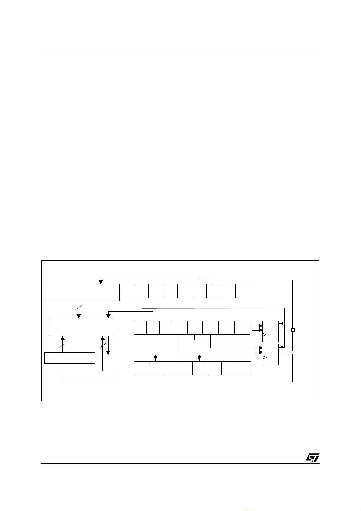
ST72561
16-BIT TIMER (Cont’d)
Notes:
1. After a processor write cycle to the OCiHR reg-
ister, the output compare function is inhibited
until the OCiLR register is also written.
2. If the OCiE bit is not set, the OCMPi pin is a
general I/O port and the OLVLi bit will not
appear when a match is f ound but an interrupt
could be generated if the OCIE bit is set.
3. When the timer clock is f
OCMPi are set while the counter value equals
the OCiR register value (see Figure 55 on page
83). This behaviour is the same in OPM or
PWM mode.
When the timer clock is f
external clock mode, OC Fi and OCMPi are set
while the counter value equals the OCiR register value plus 1 (see Figure 56 on page 83).
4. The output compare functions can be used both
for generating external events on the OCMPi
pins even if the input capture mode is also
used.
5. The value in the 16-bit OC
OLVi bit should be changed after each successful comparison in order to control an output
waveform or establish a new elapsed timeout.
/2, OCFi and
CPU
/4, f
CPU
iR register and the
CPU
/8 or in
Forced Compare Output capabilit y
When the FOLVi bit is set by software, the OLVLi
bit is copied to the OCMPi pin. The OLVi bit has to
be toggled in ord er to t oggle th e OCMPi pin when
it is enabled (OCiE bit=1). The OCFi bit is then not
set by hardware, and thus no interrupt request is
generated.
The FOLVLi bits have no effect in both one pulse
mode and PWM mode.
Figure 54. Output Compare Block Diagram
16 BIT FREE RUNNING
COUNTER
16-bit
OUTPUT COMPARE
CIRCUIT
16-bit
OC1R Register
16-bit
OC2R Register
OC1E CC0CC1
OC2E
(Control Register 2) CR2
(Control Register 1) CR1
FOLV2 FOLV1
(Status Register) SR
OLVL1OLVL2OCIE
000OCF2OCF1
Latch
1
Latch
2
OCMP1
Pin
OCMP2
Pin
82/262
Page 83
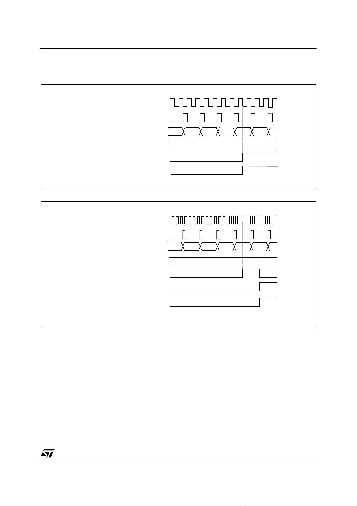
16-BIT TIMER (Cont’d)
ST72561
Figure 55. Output Compare Timing Diagram, f
INTERNAL CPU CLOC K
TIMER CLOCK
COUNTER REGISTER
OUTPUT COMPARE REGISTER i (OCRi)
OUTPUT COMPARE FLAG i (OCFi)
OCMPi PIN (OLVLi=1)
Figure 56. Output Compare Timing Diagram, f
INTERNAL CPU CLOC K
TIMER CLOCK
COUNTER REGISTER
=f
TIMER
TIMER
CPU
2ED0 2ED1 2ED2
=f
CPU
2ED0 2ED1 2ED2
/2
/4
2ED3
2ED3
2ED3
2ED42ECF
2ED42ECF
OUTPUT COMPARE REGISTER i (OCRi)
COMPARE REGISTER i LATCH
OUTPUT COMPARE FLAG i (OCFi)
OCMPi PIN (OLVLi=1)
2ED3
83/262
Page 84
ST72561
16-BIT TIMER (Cont’d)
10.4.3.5 One Pulse Mode
One Pulse mode enables the generation of a
pulse when an external event occurs. This mode is
selected via the OPM bit in the CR2 register.
The one pulse mode uses the Input Capture1
function and the Output Compare1 function.
Procedure:
To use one pulse mode:
1. Load the OC1R register with the value corresponding to the length of the pulse (see the formula in the op p os ite column) .
2. Select the following in the CR1 register:
– Using the OLVL1 bit, select the level to be ap-
plied to the OCMP1 pin after the pulse.
– Using the OLVL2 bit, select the level to be ap-
plied to the OCMP1 pin during the pulse.
– Select the edge of the a ctive tr ansition on the
ICAP1 pin with the IEDG1 bit (the ICAP1 pin
must be configured as floating input).
3. Select the following in the CR2 register:
– Set the OC1E bit, the OCMP1 pin is then ded-
icated to the Output Compare 1 function.
– Set the OPM bit.
– Select the timer clock CC[1:0] (see Table 17
Clock Control Bits).
Clearing the Input Capture in terrupt request (i.e.
clearing the ICFi bit) is done in two steps:
1. Reading the SR register while the ICFi bit is set.
2. An access (read or write) to the ICiLR register.
The OC1R register value required for a specific
timing application can be calculated usi ng the following formula:
OCiR Value =
CPU
PRESC
- 5
t
f
*
Where:
t = Pulse period (in seconds)
= CPU clock frequency (in hertz)
f
CPU
PRESC
= Timer prescaler factor (2, 4 or 8 depend-
ing on the CC[1:0] bits, see Table 17
Clock Control Bits)
If the timer clock is an external clock the formula is:
OCiR = t
* fEXT
-5
Where:
t = Pulse period (in seconds)
= External timer clock frequency (in hertz)
f
EXT
When the value of the counter is equal to the value
of the contents of t he OC1R register, the OLVL1
bit is output on the OCMP1 pin, (See Figure 57).
One pulse mode cycle
When
event occurs
on ICAP1
ICR1 = Counter
OCMP1 = OLVL2
Counter is reset
to FFFCh
ICF1 b i t is set
When
Counter
= OC1R
OCMP1 = OLVL1
Then, on a valid event on the ICAP1 pin, the counter is initialized to FFFCh and OLVL2 bit is loaded
on the OCMP1 pin, the ICF1 bit is set and the value FFFDh is loaded in the IC1R register.
Because the ICF1 bit is set when an active edge
occurs, an interrupt can be generated if the ICIE
bit is set.
Notes:
1. The OCF1 bit cannot be set by hardware in one
pulse mode but the OCF2 bit can gen erate an
Output Compare interrupt.
2. When the Pulse Width Mo dulation (PWM) and
One Pulse Mode (OPM) bits are both set, the
PWM mode is the only active one.
3. If OLVL1=OLVL2 a continuous signal will be
seen on the OCMP1 pin.
4. The ICAP1 pin can not be used to perform input
capture. The ICAP2 pin can be used t o perform
input capture (ICF2 can be set and IC2R can be
loaded) but the user must take care that the
counter is reset each time a valid edge o ccurs
on the ICAP1 pin and ICF1 can also generates
interrupt if ICIE is set.
5. When one pulse mode is used OC1R is dedicated to this mode. Nevertheless OC2R and
OCF2 can be used to indica te a period of time
has been elapsed but canno t generate an output waveform because the level OL VL 2 is dedicated to the one pulse mode.
84/262
Page 85
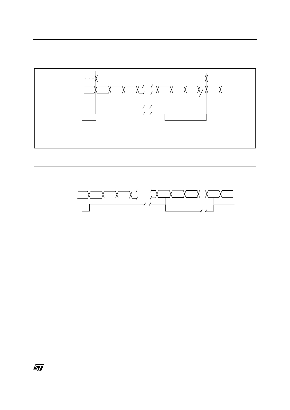
16-BIT TIMER (Cont’d)
Figure 57. One Pu lse Mode Timin g Example
ST72561
IC1R
COUNTER
ICAP1
OCMP1
01F8
FFFC FFFD FFFE 2ED0 2ED1 2ED2
01F8
OLVL2
2ED3
2ED3
FFFC FFFD
OLVL2OLVL1
compare1
Note: IEDG1=1, OC1R=2ED0h, OLVL1=0, OLVL2=1
Figure 58. Pul s e W i dt h M odulation Mode Timing E x am ple with 2 Outp ut C om pare Functi ons
COUNTER
OCMP1
FFFC FFFD FFFE
34E2
2ED0 2ED1 2ED2
OLVL2
34E2 FFFC
OLVL2OLVL1
compare2 compare1 compare2
Note: OC1R=2ED0h, OC2R=34E2, OLV L1=0, OLVL2= 1
Note: On timers with only 1 Output Compare register, a fixed frequency PWM signal can be generated us-
ing the output compare and the counter overflow to define the pulse length.
85/262
Page 86
ST72561
16-BIT TIMER (Cont’d)
10.4.3.6 Pulse Width Modulation Mode
Pulse Width Modulation (PWM) mode enables the
generation of a signal with a frequency a nd puls e
length determined by the value of the OC1R and
OC2R registers.
Pulse Width Modulation mode uses the complete
Output Compare 1 func tion plus the OC2R register, and so this functionality can not be used when
PWM mode is activated.
In PWM mode, double buffering is implemented on
the output compare registers. Any new values written in the OC1R and OC2R registers are taken
into account only a t the end of t he PWM period
(OC2) to avoid spikes on the PWM output pin
(OCMP1).
Procedure
To use pulse width modulation mode:
1. Load the OC2R register with the value corresponding to the period of the signal using the
formula in the opposite column.
2. Load the OC1R register with the value corresponding to the period of the pulse if (OLVL1=0
and OLVL2=1) using the formula in the op posite column.
3. Select the following in the CR1 register:
– Using the OLVL1 bit, select the level to be ap-
plied to the OCMP1 pin after a successful
comparison with the OC1R register.
– Using the OLVL2 bit, select the level to be ap-
plied to the OCMP1 pin after a successful
comparison with the OC2R register.
4. Select the following in the CR2 register:
– Set OC1E bit: the OCMP1 pin is then dedicat-
ed to the output compare 1 function.
– Set the PWM bit.
– Select the timer clock (CC[1:0]) (see Table 17
Clock Control Bits).
Pulse Width Modulation cycle
When
Counter
= OC1R
When
Counter
= OC2R
OCMP1 = OLVL1
OCMP1 = OLVL 2
Counter is reset
to FFFCh
If OLVL1=1 and OLVL2=0 th e length of the positive pulse is the difference between the OC2R and
OC1R registers.
If OLVL1=OLV L2 a c ontinuous signal will be seen
on the OCMP1 pin.
The OC
iR register value required for a specific tim-
ing application can be c alcul ated using the following f ormula:
OCiR Value =
CPU
PRESC
- 5
t
f
*
Where:
t = Signal or pulse period (in seconds)
= CPU clock frequency (in hertz)
f
CPU
PRESC
= Timer prescaler factor (2, 4 or 8 depend-
ing on CC[1:0] bits, see Table 17 Clock
Control Bits)
If the timer clock is an external clock the formula is:
OCiR = t
* fEXT
-5
Where:
t = Signal or pulse period (in seconds)
= External timer clock frequency (in hertz)
f
EXT
The Output Compare 2 event causes the counter
to be initialized to FFFCh (See Figure 58)
Notes:
1. After a write instruction to the OCiHR register,
the output compare function is inhibited until the
OCiLR register is also written.
2. The OCF1 and OCF2 bits cannot be set by
hardware in PWM mode therefore the Output
Compare interrupt is inhibited.
3. The ICF1 bit is set by hardware when the counter reaches the OC2R value and can produce a
timer interrupt if the ICIE bit is set and the I bit i s
cleared.
4. In PWM mode the ICAP1 pi n can not be used
to perform input capture because it is disconnected to the timer. The ICAP2 pin can be used
to perform input capture (ICF2 can be set and
IC2R can be loaded) but the user must take
care that the counter is reset ea ch period and
ICF1 can also generates interrupt if ICIE is set.
5. When the Pulse Width Mo dulation (PWM) and
One Pulse Mode (OPM) bits are both set, the
PWM mode is the only active one.
86/262
ICF1 bit is set
Page 87
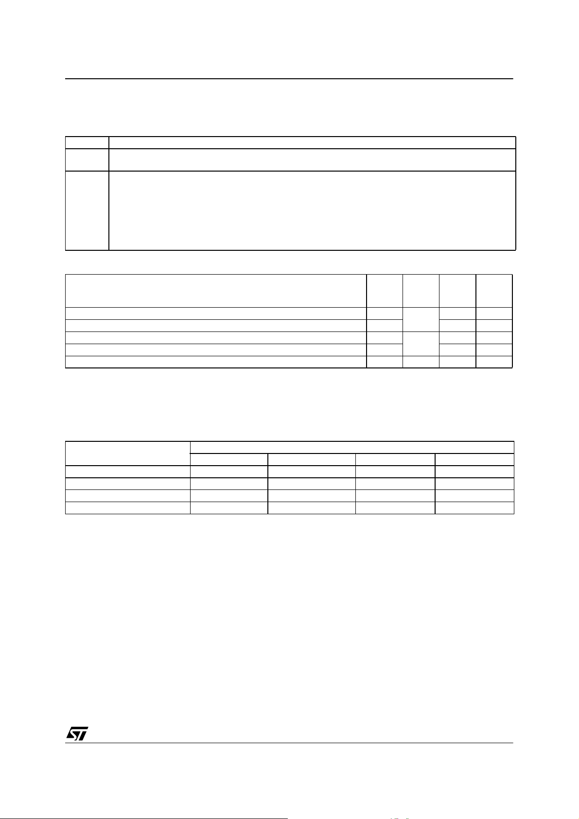
ST72561
16-BIT TIMER (Cont’d)
10.4.4 Low Power Modes
Mode Description
WAIT
HALT
10.4.5 Interrupts
Input Capture 1 event/Counter reset in PWM mode ICF1
Input Capture 2 event ICF2 Yes No
Output Compare 1 event (not available in PWM mode) OCF1
Output Compare 2 event (not available in PWM mode) OCF2 Yes No
Timer Overflow event TOF TOIE Yes No
No effect on 16-bit Timer.
Timer interrupts cause the device to exit from WAIT mode.
16-bit Timer registers are frozen.
In HALT mode, the counter stops counting until Halt mode is exited. Counting resumes from the previous
count when the MCU is woken up by an interrupt with “exit from HALT mode” capability or from the counter
reset value when the MCU is woken up by a RESET.
If an input capture event occurs on the ICAPi pin, the input capture detection circuitry is armed. Consequently, when the MCU is woken up by an interrupt with “exit from HALT mode” capability, the ICFi bit is set, and
the counter value present when exiting from HALT mode is captured into the ICiR register.
Interrupt Event
Event
Flag
Enable
Control
Bit
ICIE
OCIE
Exit
from
Wait
Yes No
Yes No
Exit
from
Halt
Note: The 16-bit Timer interrupt events are connec ted to the sa me inte rrupt vector (s ee Interrupts c hap-
ter). These events generate an interrupt if the corresponding Ena ble Control Bit is set and the interrupt
mask in the CC register is reset (RIM instruction).
10.4.6 Summary of Timer modes
MODES
Input Capture (1 and/or 2) Yes Yes Yes Yes
Output Compare (1 and/or 2) Yes Yes Yes Yes
One Pulse Mode No Not Recommended
PWM Mode No Not Recommended
Input Capture 1 Input Capture 2 Output Compare 1 Output Compare 2
TIMER RESOURCES
1)
3)
No Partially
No No
2)
1) See note 4 in Section 10.4.3.5 "One Pulse Mode"
2) See note 5 in Section 10.4.3.5 "One Pulse Mode"
3) See note 4 in Section 10.4.3.6 "Pulse Width Modulation Mode"
87/262
Page 88
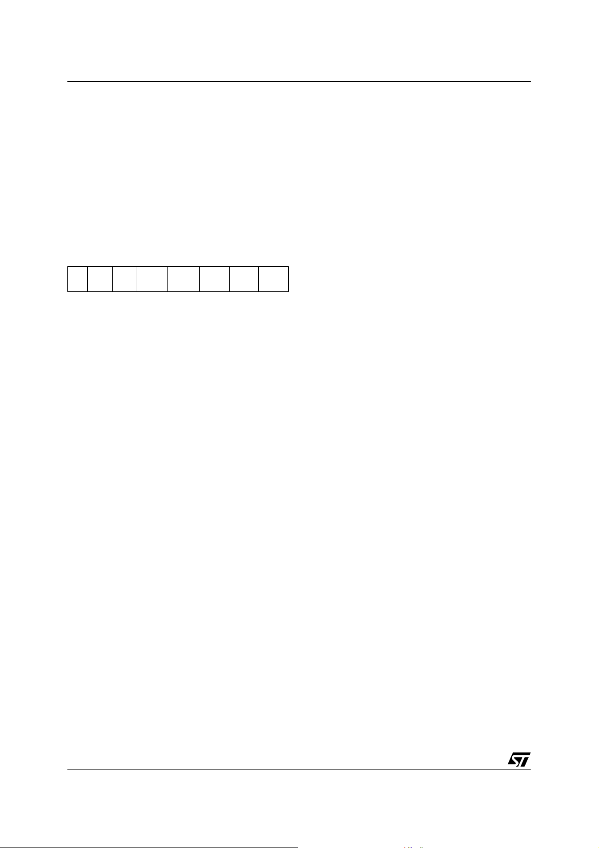
ST72561
16-BIT TIMER (Cont’d)
10.4.7 Register Description
Each Timer is associated with three control and
status registers, and with six pairs of data registers
(16-bit values) relating to the two input captures,
the two output compa res, the count er and the alternate counter.
Bit 4 = FOLV2 Forced Output Compare 2.
This bit is set and cleared by software.
0: No effect on the OCMP2 pin.
1:Forces the OLVL2 bit to be copied to the
OCMP2 pin, if the OC 2E bit is set and even if
there is no successful compari so n.
CONTROL REGISTER 1 (CR1)
Read/Write
Reset Value: 0000 0000 (00h)
70
ICIE OCIE TOIE FOLV2 FOLV1 OLVL2 IEDG1 OLVL1
Bit 3 = FOLV1 Forced Output Compare 1.
This bit is set and cleared by software.
0: No effect on the OCMP1 pin.
1: Forces OLVL1 to be copied to the OCMP1 pin, if
the OC1E bit is set and e ven if there is no successful comparison.
Bit 2 = OLVL2 Output Level 2.
Bit 7 = ICIE Input Capture Interrupt Enable.
0: Interrupt is inhibited.
1: A timer interrupt is generated whenever the
ICF1 or ICF2 bit of the SR register is set.
Bit 6 = OCIE Output Compare Interrupt Enable.
0: Interrupt is inhibited.
1: A timer interrupt is generated whenever the
OCF1 or OCF2 bit of the SR register is set.
This bit is copied to the OCMP2 pin wh enever a
successful compa rison occurs with the OC2R register and OCxE is set in the CR2 register. This value is copied to the OCMP1 pin in One Pulse Mode
and Pulse Width Modulation mode.
Bit 1 = IEDG1 Input Edge 1.
This bit determines wh ich type of level transition
on the ICAP1 pin will trigger the capture.
0: A falling edge triggers the capture.
1: A rising edge triggers the capture.
Bit 5 = TOIE Timer Overflow Interrupt Enable.
0: Interrupt is inhibited.
1: A timer interrupt is enabled whenever the TOF
bit of the SR register is set.
Bit 0 = OLVL1 Output Level 1.
The OLVL1 bit i s copied to the OCMP1 pin whenever a successful comparison occurs with the
OC1R register and the OC1E bit is set in th e CR2
register.
88/262
Page 89
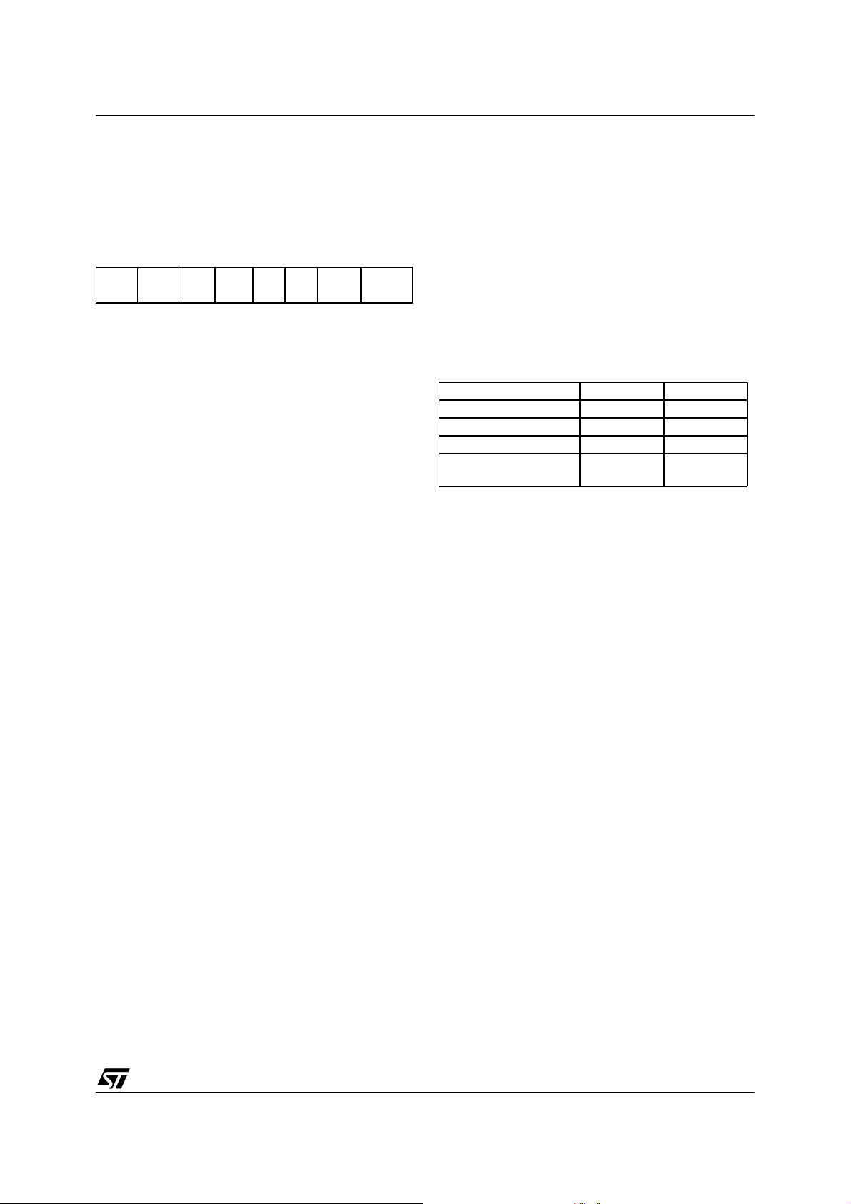
16-BIT TIMER (Cont’d)
CONTROL REGISTER 2 (CR2)
Read/Write
Reset Value: 0000 0000 (00h)
70
OC1E OC2E OPM PWM CC1 CC0 IEDG2 EXEDG
Bit 4 = PWM Pulse Width Modulation.
0: PWM mode is not active.
1: PWM mode is active, the OCMP1 pin outputs a
programmable cyclic signal; the length of the
pulse depends on the value of OC1R register;
the period depends on the value of OC2R register.
ST72561
Bit 7 = OC1E Output Compare 1 Pin Enable.
This bit is used only to outp ut the signal from the
timer on the OCMP1 pin (OLV1 in Output Compare mode, both OLV1 and OLV2 in PWM and
one-pulse mode). Whatever the value of the OC1E
bit, the Output Compare 1 function of the timer remains active.
0: OCMP1 pin alternate f unction disabled (I/O pin
free for general-purpose I/O).
1: OCMP1 pin alternate function enabled.
Bit 6 = OC2E Output Compare 2 Pin Enable.
This bit is used only to outp ut the signal from the
timer on the OCMP2 pin (OLV2 in Output Compare mode). Whatever the value of the OC2E bit,
the Output Compare 2 function of the timer remains active.
0: OCMP2 pin alternate f unction disabled (I/O pin
free for general-purpose I/O).
1: OCMP2 pin alternate function enabled.
Bit 5 = OPM One Pulse Mode.
0: One Pulse Mode is not active.
1: One Pulse Mode is active, the ICAP1 pin can be
used to trigger one pulse on the OCMP1 pin; the
active transition is g iven by the IE DG1 bit. The
length of the generated pulse depends on the
contents of the OC1R register.
Bit 3, 2 = CC[1:0] Clock Control.
The timer clock mode depends on these bits:
Table 17. Clock Control Bits
Timer Clock CC1 CC0
f
/ 4 0 0
CPU
f
/ 2 0 1
CPU
f
/ 8 1 0
CPU
External Clock (where
available)
11
Note: If the external clock pin is not available, programming the external clock configuration stops
the counter.
Bit 1 = IEDG2 Input Edge 2.
This bit determines wh ich type of level transition
on the ICAP2 pin will trigger the capture.
0: A falling edge triggers the capture.
1: A rising edge triggers the capture.
Bit 0 = EXEDG External Clock Edge.
This bit determines wh ich type of level transition
on the external clock pin EXTCLK wi ll trigger the
counter register.
0: A falling edge triggers the counter register.
1: A rising edge triggers the counter register.
89/262
Page 90

ST72561
16-BIT TIMER (Cont’d)
CONTROL/STATUS REGISTER (CSR)
Read/Write (bits 7:3 read only)
Reset Value: xxxx x0xx (xxh)
70
ICF1 OCF1 TOF ICF2 OCF2 TIMD 0 0
Bit 7 = ICF1 Input Capture Flag 1.
0: No input capture (reset value).
1: An input capture has occurred on the ICAP1 pin
or the counter has reached th e OC2R value in
PWM mode. To clear this bit, first read the SR
register, then read or write the low by te of the
IC1R (IC1LR) register.
Bit 6 = OCF1 Output Compare Flag 1.
0: No match (reset value).
1: The content of the free running counter has
matched the content of the OC1R register. To
clear this bit, first read the SR register, t hen read
or write the low byte of the OC1R (OC1LR) register.
Bit 5 = TOF Timer Overflow Flag.
0: No timer overflow (reset value).
1:The free running counter rolled over from FFFFh
to 0000h. To clear this bit, first read the SR register, then read or write the low byte of the CR
(CLR) register.
Note: Reading or writing the ACLR reg ister does
not clear TOF.
Bit 4 = ICF2 Input Capture Flag 2.
0: No input capture (reset value).
1: An input capture has occurred on the ICAP2
pin. To clear this bit, first read the SR register,
then read or write the low byte of the IC2R
(IC2LR) register.
Bit 3 = OCF2 O utput Compare Fl ag 2.
0: No match (reset value).
1: The content of the free running counter has
matched the c ontent of the OC2R register. T o
clear this bit, first read the SR register, then read
or write the low byte of the OC2R (OC2LR) register.
Bit 2 = TIMD Timer disable.
This bit is set and cleared by software. When set, it
freezes the timer prescaler an d counter and disabled the output functions (OCMP1 and OCMP2
pins) to reduce power consumption. Access to the
timer registers is still available, allowing t he timer
configuration to be changed, or the counter res et,
while it is disabled.
0: Timer enabled
1: Timer prescaler, counter and outputs disabled
Bits 1:0 = Reserved, must be kept cleared.
90/262
Page 91
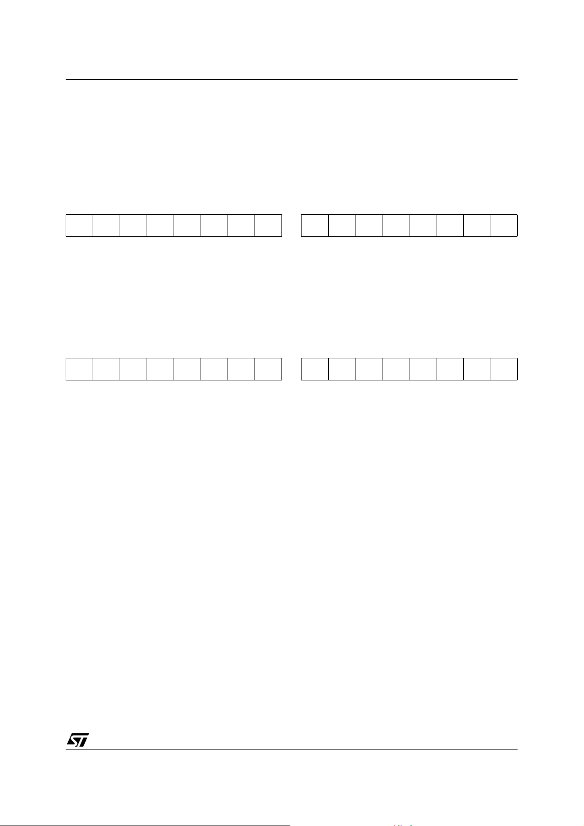
16-BIT TIMER (Cont’d)
INPUT CAPTURE 1 HIGH REGISTER (IC1HR)
Read Only
Reset Value: Undefined
This is an 8-bit read only register that contains the
high part of the counter value (transferred by the
input capture 1 event).
ST72561
OUTPUT COMPARE 1 HIGH REGISTER
(OC1HR)
Read/Write
Reset Value: 1000 0000 (80h)
This is an 8-bit register that contains the high part
of the value to be compared to the CHR register.
70
MSB LSB
INPUT CAPTURE 1 LOW REGISTER (IC1LR)
Read Only
Reset Value: Undefined
This is an 8-bit read only register that contains the
low part of the counter value (transferred by the input capture 1 event).
70
MSB LSB
70
MSB LSB
OUTPUT COMPARE 1 LOW REGISTER
(OC1LR)
Read/Write
Reset Value: 0000 0000 (00h)
This is an 8-bit register that contains the low part of
the value to be compared to the CLR register.
70
MSB LSB
91/262
Page 92
ST72561
16-BIT TIMER (Cont’d)
OUTPUT COMPARE 2 HIGH REGISTER
(OC2HR)
Read/Write
Reset Value: 1000 0000 (80h)
This is an 8-bit register that c ontains the high part
of the value to be compared to the CHR register.
ALTERNATE COUNTER HIGH REGISTER
(ACHR)
Read Only
Reset Value: 1111 1111 (FFh)
This is an 8-bit register that contains the high part
of the counter value.
70
MSB LSB
OUTPUT COMPARE 2 LOW REGISTER
(OC2LR)
Read/Write
Reset Value: 0000 0000 (00h)
This is an 8-bit register that contains the low part of
the value to be compared to the CLR register.
70
70
MSB LSB
ALTERNATE COUNTER LOW REGISTER
(ACLR)
Read Only
Reset Value: 1111 1100 (FCh)
This is an 8-bit register that contains the low part of
the counter value. A write to this register resets the
counter. An access to this register after an access
to CSR register does no t clear the TOF bit i n the
CSR register.
MSB LSB
COUNTER HIGH REGISTER (CHR)
70
MSB LSB
Read Only
Reset Value: 1111 1111 (FFh)
This is an 8-bit register that c ontains the high part
of the counter value.
70
INPUT CAPTURE 2 HIGH REGISTER (IC2HR)
Read Only
Reset Value: Undefined
This is an 8-bit read only register that contains the
high part of the counter value (transferred by the
MSB LSB
Input Capture 2 event).
70
COUNTER LOW REGISTER (CLR)
MSB LSB
Read Only
Reset Value: 1111 1100 (FCh)
This is an 8-bit register that contains the low part of
the counter value. A write to this register resets the
counter. An access to this register after accessing
the CSR register clears the TOF bit.
70
INPUT CAPTURE 2 LOW REGISTER (IC2LR)
Read Only
Reset Value: Undefined
This is an 8-bit read only register that contains the
low part of the counter value (transferred by the Input Capture 2 event).
MSB LSB
92/262
70
MSB LSB
Page 93
16-BIT TIMER (Cont’d)
Table 18. 16-Bit Timer Register Map
ST72561
Address
(Hex.)
51 CR2 OC1E OC2E OPM PWM CC1 CC0 IEDG2 EXEDG
52 CR1 ICIE OCIE TOIE FOLV2 FOLV1 OLVL2 IEDG1 OLVL1
53 CSR ICF1 OCF1 TOF ICF2 OCF2 TIMD
54 IC1HR MSB LSB
55 IC1LR MSB LSB
56 OC1HR MSB LSB
57 OC1LR MSB LSB
58 CHR MSB LSB
59 CLR MSB LSB
5A ACHR MSB LSB
5B ACLR MSB LSB
5C IC2HR MSB LSB
5D IC2LR MSB LSB
5E OC2HR MSB LSB
5F OC2LR MSB LSB
Register
Name
76543210
93/262
Page 94

ST72561
10.5 8-BIT TIMER (TIM8)
10.5.1 Introduction
The timer consists of a 8-bit free-running counter
driven by a programmable prescaler.
It may be used for a variety of purposes, including
pulse length measurement of up to two input signals (input capture) or generation of up to two out-
put waveforms (output compare and PWM).
Pulse lengths and waveform perio ds can be modulated from a few microseconds to several milliseconds using the timer prescaler and the clock
prescaler.
10.5.2 Main Features
■ Programmable prescaler: f
or f
■ Overflow status flag and maskable interrupt
■ Output compare functions with
divided by 8000.
OSC2
divided by 2, 4 , 8
CPU
– 2 dedicated 8-bit registers
– 2 dedicated programmable signals
– 2 dedicated status flags
– 1 dedicated maskable interrupt
■ Input capture functions with
– 2 dedicated 8-bit registers
– 2 dedicated active edge selection signals
– 2 dedicated status flags
– 1 dedicated maskable interrupt
■ Pulse width modulation mode (PWM)
■ One pulse mode
■ Reduced Power Mode
■ 4 alternate functions on I/O ports (ICAP1, ICAP2,
OCMP1, OCMP2)*
When reading an input signal on a non-bonded
pin, the value will always be ‘1’.
10.5.3 Functional Description
10.5.3.1 Counter
The main block of the Programmable Timer is a 8bit free running u pco unter and its associated 8-bit
registers.
These two read-only 8-bit registers contain the
same value but with the difference that reading the
ACTR register does not clear the TOF bit (Timer
overflow flag), located in the Status register, (SR).
Writing in the CTR register or ACTR register resets the free running counter to the FCh value.
Both counters have a reset value of FCh (this is
the only value which is reloaded in the 8-bit timer).
The reset value of both counters is also FCh in
One Pulse mode and PWM mode.
The timer clock depends on the clock con trol bits
of the CR2 register, as shown in Table 19 Clock
Control Bits. The value in the c ounter register re-
peats every 512, 1024, 2048 or 20480000 f
CPU
clock cycles depending on the CC[1:0] bits.
The timer frequency can be f
or f
For example, if f
f
OSC2
/8000.
OSC2
/8000 is selected, and
OSC2
=8 MHz, the timer frequency will be 1 ms.
CPU
/2, f
CPU
/4, f
CPU
/8
Refer to Table 19 on page 108.
The Block Diagram is shown in Figure 59.
*Note: So me time r pin s m ay not be available (not
bonded) in some ST7 devices. Refer to the device
pin out description.
94/262
Page 95
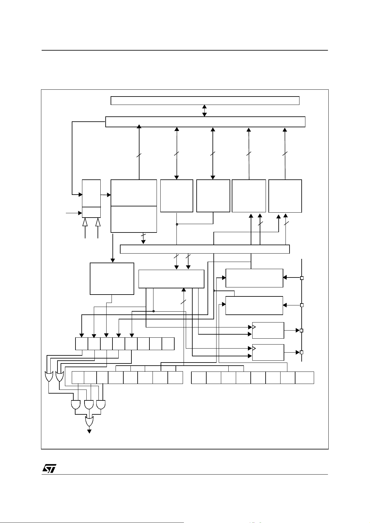
8-BI T TIMER (Cont’d)
Figure 59. Tim er B l ock Di a gra m
f
CPU
ST72561
ST7 INTERNAL BUS
MCU-PERIPHERAL INTERFACE
f
OSC2
1/2
1/4
1/8
1/8000
CC[1:0]
COUNTER
REGISTER
ALTERNATE
COUNTER
REGISTER
OVERFLOW
DETECT
CIRCUIT
ICF2ICF1
OCF2OCF1 TOF
(Control/Status Register)
8
OUTPUT
COMPARE
REGISTER
1
8
TIMER INTERNAL BUS
OUTPUT COMPARE
CIRCUIT
6
0
0
TIMD
CSR
8
8 8
8
OUTPUT
COMPARE
REGISTER
2
8
INPUT
CAPTURE
REGISTER
1
8
EDGE DETECT
CIRCUIT1
EDGE DETECT
CIRCUIT2
LATCH1
LATCH2
8
INPUT
CAPTURE
REGISTER
2
8
ICAP1
pin
ICAP2
pin
OCMP1
pin
OCMP2
pin
(See note)
TIMER INTERRUPT
(Control Register 1) CR1
Note: If IC, OC and TO interrupt requests have separate vectors
then the last O R is not presen t (See device Interrupt Vector Table)
OC2E
PWMOC1E
OPMFOLV2ICIE OLVL1IEDG1OLVL2FOLV1OCIE TOIE
IEDG2CC0CC1
0
(Control Register 2) CR2
95/262
Page 96

ST72561
8-BI T TIMER (Cont’d)
Whatever the timer mode used (input capture, output compare, one pulse mode or PWM mode) an
overflow occurs when the counter rolls over from
FFh to 00h then:
– The TOF bit of the SR register is set.
– A timer interrupt is generated if:
– TOIE bit of the CR1 register is set and
– I bit of the CC register is cleared.
If one of these cond itions is false, the interrupt remains pending to be issued as soon as they are
both true.
Clearing the overflow interrupt request is done in
two steps:
1.Reading the SR register while the TOF bit is set.
2.An access (read or write) to the CTR register.
Notes: The TOF bit is not cleared by accesses to
ACTR register. The advantage of accessing the
ACTR register rather than the CTR register is that
it allows simultaneous use of the overflow function
and reading the free running counter at random
times (for example, to measure elapsed time) without the risk of clearing the TOF bit erroneously.
The timer is not affected by WAIT mode.
In HALT mode, the counter stops counting until the
mode is exited. Counting then resumes from the
previous count (MCU awakened by an interrupt) or
from the reset count (MCU awakened by a Reset).
96/262
Page 97
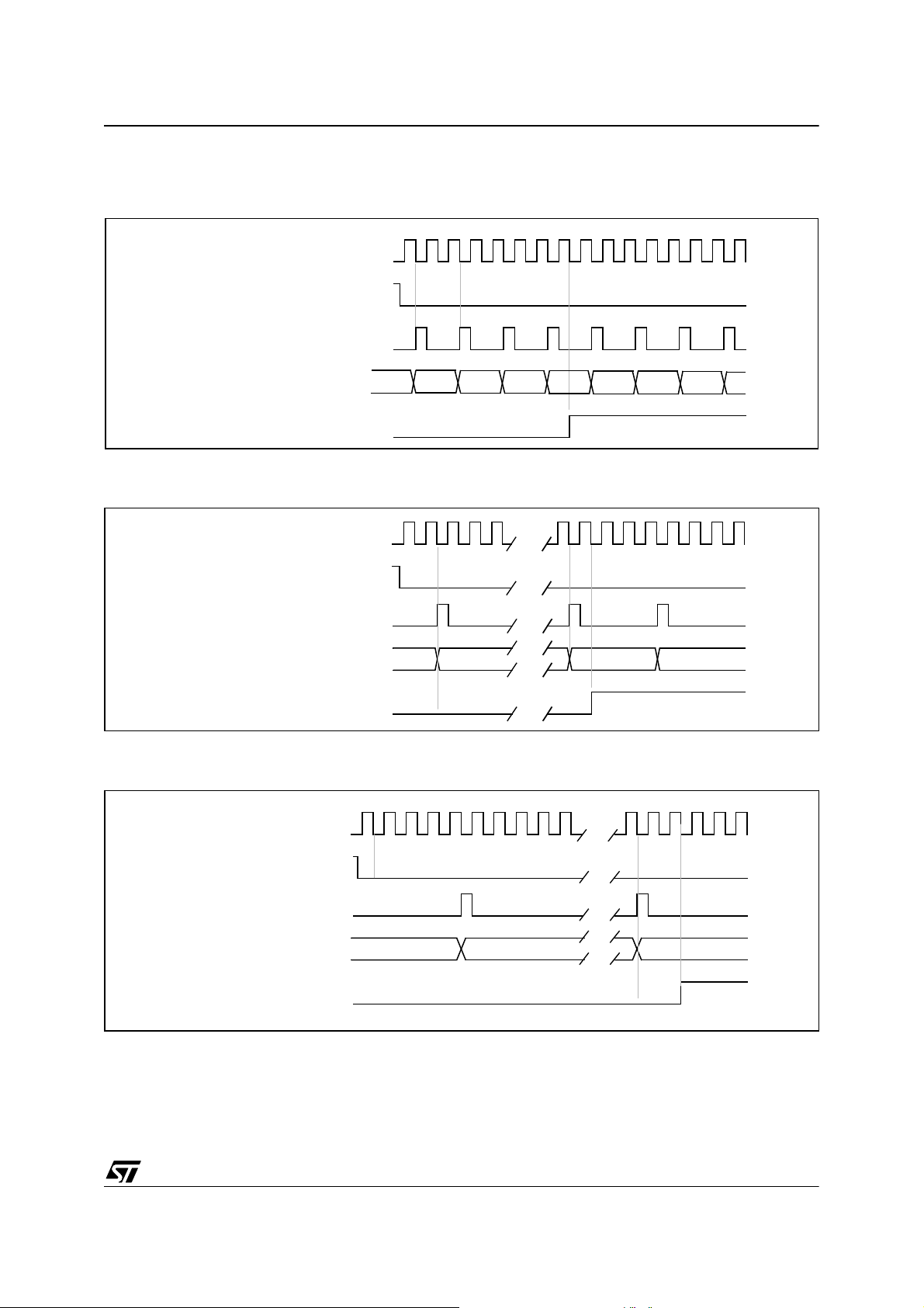
8-BI T TIMER (Cont’d)
Figure 60. Counter Timing Diagram, internal clock divided by 2
f
CLOCK
CPU
INTERNAL RESET
TIMER CLOCK
ST72561
COUNTER REGISTER
TIMER OVERFLOW FLAG (TOF)
FD FE FF 00 01 02 03
Figure 61. Counter Timing Diagram, internal clock divided by 4
f
CLOCK
CPU
INTERNAL RESET
TIMER CLOCK
COUNTER REGI STER
TIMER OVERFLOW FLAG (TOF)
FC FD 00 01
Figure 62. Counter Timing Diagram, internal clock divided by 8
f
CLOCK
CPU
INTERNAL RESET
TIMER CLOCK
COUNTER REGISTER
TIMER OVERFLOW FLAG (TOF)
FC FD
00
Note: The MCU is in reset state when the internal reset signal is high, when it is low the MCU is running.
97/262
Page 98

ST72561
8-BI T TIMER (Cont’d)
10.5.3.2 Input Capture
In this section, the index, i, may be 1 or 2 because
there are 2 input capture functions in the 8-bit timer.
The two 8-bit input capture registers (IC1R and
IC2R) are used to latch the valu e of the free running counter after a transition is detected on the
ICAPi pin (see figure 5).
ICiR register is a read-only register.
The active transition is software programmable
through the IEDGi bit of Control Registers (CRi).
Timing resolution is one count of the free running
counter (see Table 19 Clock Control Bits).
When an input capture occurs:
– IC Fi bit is set.
– Th e ICiR register contains the value of the free
running counter on the active transition on the
ICAPi pin (see Figure 64).
– A timer interrupt is generated if the ICIE bit is set
and the interrrupt mask is cleared in the CC register. Otherwise, the interrupt remains pending
until both conditions become true.
Clearing the Input Capture in terrupt request (i.e.
clearing the ICFi bit) is done in two steps:
1. Reading the SR register while the ICFi bit is set.
2. An access (read or write) to the ICiR register.
Procedure:
To use the input capture function select the following in the CR2 register:
– Select the timer clock (CC[1:0]) (see Table 19
Clock Control Bits).
– Select the edge of the active transition o n the
ICAP2 pin with the IEDG2 bit (the ICAP2 pin
must be configured as floating input or input with
pull-up without interrupt if this configuration is
available).
And select the following in the CR1 register:
– Set the IC IE b it to generat e an in terrupt after a n
input capture com ing from e ither the ICAP1 pin
or the ICAP2 pin
– Select the edge of the active transition o n the
ICAP1 pin with the IEDG1 bit (the ICAP1 pin
must be configured as floating input or input with
pull-up without interrupt if this configuration is
available).
Notes:
6. The ICiR register contains the free running
counter value which corresponds to the most
recent input capture.
7. The 2 input capture functions can be used
together even if the timer also uses the 2 output
compare functions.
8. Once the ICIE bit is set both input capture features may trigger interrupt reque sts. If only one
is needed in the ap plication, the interrupt routine software needs to discard the unwanted
capture interrupt. This can be done by checking
the ICF1 and ICF2 flags and resetting them
both.
9. In One pulse Mode and PWM mode only Input
Capture 2 can be used.
10.The alternate inputs (ICAP1 & ICAP2) are
always directly connec ted to the timer. So any
transitions on these pins activates the input
capture function.
Moreover if one of the ICAPi pins is configured
as an input and t he second one as an output,
an interrupt can be generated if the user toggles the output pin and if the ICIE bit is set.
11.The TOF bit can be used with interrupt generation in order to m easure events t hat go bey ond
the timer range (FFh).
98/262
Page 99
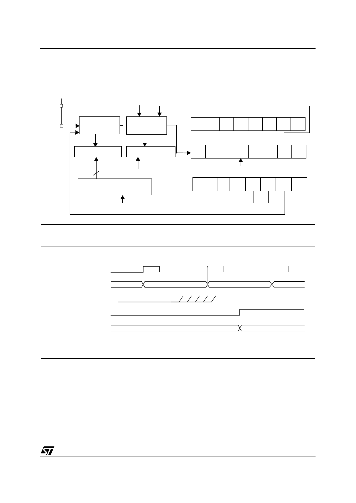
8-BI T TIMER (Cont’d)
Figure 63. Input Capture Block Diagram
ST72561
ICAP1
pin
ICAP2
pin
EDGE DETECT
CIRCUIT2
IC2R Register
8-bit
8-bit FREE RUNNING
COUNTER
EDGE DETECT
CIRCUIT1
IC1R Register
Figure 64. Input Capture Timing Diagram
TIMER CLOCK
ICIE
(Control Register 1) CR1
IEDG1
(Status Register) SR
ICF2ICF1 000
(Control Register 2) CR2
IEDG2
CC0
CC1
COUNTER REGISTER
ICAPi PIN
ICAPi FLAG
ICAPi REGISTER
Note: The rising edge is the active edge.
01 02 03
03
99/262
Page 100

ST72561
8-BI T TIMER (Cont’d)
10.5.3.3 Output Compare
In this section, the index, i, may be 1 or 2 because
there are 2 out put compare functions in the 8-bit
timer.
This function can be used to control an output
waveform or indicate when a period of time has
elapsed.
When a match is found bet ween the Out put Com pare register and the free running counter, the output compare function:
– Assigns pins with a programmable value if the
OCiE bit is set
– Sets a flag in the status register
– Generates an interrupt if enabled
Two 8-bit registers Output Compare Register 1
(OC1R) and Output Compare Register 2 (OC2R)
contain the value to be com pared to the counter
register each timer clock cycle.
These registers are readable and writable and are
not affected by the timer hardware. A reset event
changes the OC
Timing resolution is one count of the free running
counter: (f
Procedure:
To use the output compare function, select the following in the CR2 register:
– Set the OCiE bit if an output is needed then the
OCMPi pin i s dedicated to the output com pare i
signal.
– Select the timer clock (CC[1:0]) (see Table 19
Clock Control Bits).
And select the following in the CR1 register:
iR value to 00h.
CPU/CC[1:0]
).
– Select the OLVLi bit to applied to the OCMPi pins
after the match occurs.
– Set the OCIE bit t o generate an interrupt if it is
needed.
When a match is found between OCRi register
and CR register:
– OCF i b i t is set.
– The OCMP i pin take s OLVL i bit value (OCMPi
pin latch is forced low during reset).
– A timer interrupt is generated if the OCIE bit is
set in the CR1 register and the I bit is cleared in
the CC register (CC).
The OC
iR register value required for a specific tim-
ing application can be c alcul ated using the following f ormula:
∆t * f
∆ OCiR =
CPU
PRESC
Where:
∆t = Output compare period (in seconds)
f
= P LL output x2 clock frequency in h ertz
CPU
PRESC
(or f
= Timer prescaler factor (2, 4, 8 or 8000
depending on CC[1:0] bits, see Table
19 Clock Control Bits)
Clearing the output compare interrupt request (i.e.
clearing the OCFi bit) is done by:
1. Reading the SR register while the OCFi bit is
set.
2. An access (read or write) to the OCiR register.
/2 if PLL is not enabled)
OSC
100/262
 Loading...