

ST6253C ST6263C ST6263B
PDIP20
PSO20
CDIP20W
(See end of Datasheet for Ordering Information)
safe reset, auto-reload timer, EEPROM and SPI
Features
■ 3.0 to 6.0 V Supply Operating Range
■ 8 MHz Maximum Clock Frequency
■ -40 to +125°C Operating Temperature Range
■ Run, Wait and Stop Modes
■ 5 Interrupt Vectors
■ Look-up Table capability in Program Memory
■ Data Storage in Program Memory:
User selectable size
■ Data RAM: 128 bytes
■ Data EEPROM: 64/128 bytes (not in ST6253C
devices)
■ User Programmable Options
■ 13 I/O pins, fully programmable as:
– Input with pull-up resistor
– Input without pull-up resistor
– Input with interrupt generation
– Open-drain or push-pull output
– Analog Input
■ 6 I/O lines can sink up to 30 mA to drive LEDs or
TRIACs directly
■ 8-bit Timer / Counter with 7-bit programmable
prescaler
■ 8-bit Auto-reload Timer with 7-bit programmable
prescaler (AR Timer)
■ Digital Watchdog
■ Oscillator Safe Guard (not in ROM devices)
■ Low Voltage Detector for Safe Reset (not in
ROM devices)
■ 8-bit A/D Converter with 7 analog inputs
■ 8-bit Synchronous Peripheral Interface (SPI)
■ On-chip Clock oscillator can be driven by Quartz
Crystal Ceramic resonator or RC network
■ User configurable Power-on Reset
■ One external Non-Maskable Interrupt
■ ST626x-EMU2 Emulation and Development
System (connects to an MS-DOS PC via a
parallel port).
ST6260C ST6260B
8-bit MCUs with A/D converter,
DEVICE SUMMARY
DEVICE
ST6253C 1836 ST6260C / ST6260B 3884 128
ST6263C / ST6263B 1836 64
Program memory
(Bytes)
EEPROM
(Bytes)
March 2009 Rev. 3 1/83

Table of Contents
Document
Page
ST6253C ST6263C ST6263B
ST6260C ST6260B . . . . . . . . . . . . . . . . . . . . . . . . . . . . . . . . . . . . . 1
1 GENERAL DESCRIPTION . . . . . . . . . . . . . . . . . . . . . . . . . . . . . . . . . . . . . . . . . . . . . . . . . . . . . . 4
1.1 INTRODUCTION . . . . . . . . . . . . . . . . . . . . . . . . . . . . . . . . . . . . . . . . . . . . . . . . . . . . . . . . . 4
1.2 PIN DESCRIPTIONS . . . . . . . . . . . . . . . . . . . . . . . . . . . . . . . . . . . . . . . . . . . . . . . . . . . . . . 5
1.3 MEMORY MAP . . . . . . . . . . . . . . . . . . . . . . . . . . . . . . . . . . . . . . . . . . . . . . . . . . . . . . . . . . 6
1.4 PROGRAMMING MODES . . . . . . . . . . . . . . . . . . . . . . . . . . . . . . . . . . . . . . . . . . . . . . . . . 13
2 CENTRAL PROCESSING UNIT . . . . . . . . . . . . . . . . . . . . . . . . . . . . . . . . . . . . . . . . . . . . . . . . . 15
2.1 INTRODUCTION . . . . . . . . . . . . . . . . . . . . . . . . . . . . . . . . . . . . . . . . . . . . . . . . . . . . . . . . 15
2.2 CPU REGISTERS . . . . . . . . . . . . . . . . . . . . . . . . . . . . . . . . . . . . . . . . . . . . . . . . . . . . . . . 15
3 CLOCKS, RESET, INTERRUPTS AND POWER SAVING MODES . . . . . . . . . . . . . . . . . . . . . 17
3.1 CLOCK SYSTEM . . . . . . . . . . . . . . . . . . . . . . . . . . . . . . . . . . . . . . . . . . . . . . . . . . . . . . . . 17
3.2 RESETS . . . . . . . . . . . . . . . . . . . . . . . . . . . . . . . . . . . . . . . . . . . . . . . . . . . . . . . . . . . . . . . 22
3.3 DIGITAL WATCHDOG . . . . . . . . . . . . . . . . . . . . . . . . . . . . . . . . . . . . . . . . . . . . . . . . . . . . 26
3.4 INTERRUPTS . . . . . . . . . . . . . . . . . . . . . . . . . . . . . . . . . . . . . . . . . . . . . . . . . . . . . . . . . . 30
3.5 POWER SAVING MODES . . . . . . . . . . . . . . . . . . . . . . . . . . . . . . . . . . . . . . . . . . . . . . . . . 34
4 ON-CHIP PERIPHERALS . . . . . . . . . . . . . . . . . . . . . . . . . . . . . . . . . . . . . . . . . . . . . . . . . . . . . . 36
4.1 I/O PORTS . . . . . . . . . . . . . . . . . . . . . . . . . . . . . . . . . . . . . . . . . . . . . . . . . . . . . . . . . . . . . 36
4.2 TIMER . . . . . . . . . . . . . . . . . . . . . . . . . . . . . . . . . . . . . . . . . . . . . . . . . . . . . . . . . . . . . . . . 42
4.3 AUTO-RELOAD TIMER . . . . . . . . . . . . . . . . . . . . . . . . . . . . . . . . . . . . . . . . . . . . . . . . . . . 45
4.4 A/D CONVERTER (ADC) . . . . . . . . . . . . . . . . . . . . . . . . . . . . . . . . . . . . . . . . . . . . . . . . . 51
4.5 SERIAL PERIPHERAL INTERFACE (SPI) . . . . . . . . . . . . . . . . . . . . . . . . . . . . . . . . . . . . 53
4.6 SPI TIMING DIAGRAMS . . . . . . . . . . . . . . . . . . . . . . . . . . . . . . . . . . . . . . . . . . . . . . . . . . 56
5 SOFTWARE . . . . . . . . . . . . . . . . . . . . . . . . . . . . . . . . . . . . . . . . . . . . . . . . . . . . . . . . . . . . . . . . 58
5.1 ST6 ARCHITECTURE . . . . . . . . . . . . . . . . . . . . . . . . . . . . . . . . . . . . . . . . . . . . . . . . . . . . 58
5.2 ADDRESSING MODES . . . . . . . . . . . . . . . . . . . . . . . . . . . . . . . . . . . . . . . . . . . . . . . . . . . 58
5.3 INSTRUCTION SET . . . . . . . . . . . . . . . . . . . . . . . . . . . . . . . . . . . . . . . . . . . . . . . . . . . . . . 59
6 ELECTRICAL CHARACTERISTICS . . . . . . . . . . . . . . . . . . . . . . . . . . . . . . . . . . . . . . . . . . . . . . 64
6.1 ABSOLUTE MAXIMUM RATINGS . . . . . . . . . . . . . . . . . . . . . . . . . . . . . . . . . . . . . . . . . . . 64
6.2 RECOMMENDED OPERATING CONDITIONS . . . . . . . . . . . . . . . . . . . . . . . . . . . . . . . . . 65
6.3 DC ELECTRICAL CHARACTERISTICS . . . . . . . . . . . . . . . . . . . . . . . . . . . . . . . . . . . . . . 66
6.4 AC ELECTRICAL CHARACTERISTICS . . . . . . . . . . . . . . . . . . . . . . . . . . . . . . . . . . . . . . 67
6.5 A/D CONVERTER CHARACTERISTICS . . . . . . . . . . . . . . . . . . . . . . . . . . . . . . . . . . . . . . 68
6.6 TIMER CHARACTERISTICS . . . . . . . . . . . . . . . . . . . . . . . . . . . . . . . . . . . . . . . . . . . . . . . 68
6.7 SPI CHARACTERISTICS . . . . . . . . . . . . . . . . . . . . . . . . . . . . . . . . . . . . . . . . . . . . . . . . . 68
6.8 ARTIMER ELECTRICAL CHARACTERISTICS . . . . . . . . . . . . . . . . . . . . . . . . . . . . . . . . . 68
7 PACKAGE MECHANICAL DATA . . . . . . . . . . . . . . . . . . . . . . . . . . . . . . . . . . . . . . . . . . . . . . . . 74
8 ORDERING INFORMATION . . . . . . . . . . . . . . . . . . . . . . . . . . . . . . . . . . . . . . . . . . . . . . . . . . . . 76
8.1 OTP/EPROM VERSIONS . . . . . . . . . . . . . . . . . . . . . . . . . . . . . . . . . . . . . . . . . . . . . . . . . 76
8.2 FASTROM VERSIONS . . . . . . . . . . . . . . . . . . . . . . . . . . . . . . . . . . . . . . . . . . . . . . . . . . . 77
8.3 ROM VERSIONS . . . . . . . . . . . . . . . . . . . . . . . . . . . . . . . . . . . . . . . . . . . . . . . . . . . . . . . . 78
2/83

Table of Contents
9 REVISION HISTORY . . . . . . . . . . . . . . . . . . . . . . . . . . . . . . . . . . . . . . . . . . . . . . . . . . . . . . . . . . 82
Document
Page
3/83

ST6253C ST6263C ST6263B ST6260C ST6260B
TEST
NMI
INTERRUPT
PROGRAM
PC
STACK LEVEL 1
STACK LEVEL 2
STACK LEVEL 3
STACK LEVEL 4
STACK LEVEL 5
STACK LEVEL 6
POWER
SUPPLY
OSCILLATOR
RESET
DATA ROM
USER
SELECTABLE
DATA RAM
PORT A
PORT B
TIMER
DIGITAL
8 BIT CORE
TEST/V
PP
8-BIT
A/D CONVERTER
PA0..PA3 / Ain
PB0..PB3 / 30 mA Sink
VDDV
SS
OSCin OSCout RESET
WATCHDOG
MEMORY
PB6 / ARTimin / 30 mA Sink
PORT C
PC2 / Sin / Ain
PC3 / Sout / Ain
SPI (SERIAL
PERIPHERAL
INTERFACE)
AUTORELOAD
TIMER
PC4 / Sck / Ain
PB7 / ARTimout / 30 mA Sink
128 Bytes
1836 bytes OTP
3884 bytes OTP
3884 bytes EPROM
(ST62T53C,T63C)
(ST62T60C)
(ST62E60C)
DATA EEPROM
64 Bytes
128 Bytes
(ST62T60C/E60C)
(ST62T63C)
1 GENERAL DESCRIPTION
1.1 INTRODUCTION
The ST62T53C, ST62T60C, ST62T63C and
ST62E60C devices are low cost members of the
ST62xx 8-bit HCMOS family of microcontrollers,
which is targeted at low to medium complexity ap
plications. All ST62xx devices are based on a
building block approach: a common core is sur
rounded by a number of on-chip peripherals.
The ST62E60C is the erasable EPROM version of
the ST62T60C device, which may be used to em
ulate the ST62T53C, ST62T60C and ST62T63C
devices, as well as the respective ST6253C,
ST6260B and ST6263B ROM devices.
OTP and EPROM devices are functionally identical. The ROM based versions offer the same functionality selecting as ROM options the options de-
Figure 1. Block Diagram
-
-
-
fined in the programmable option byte of the OTP/
EPROM versions.
OTP devices offer all the advantages of user programmability at low cost, which make them the
ideal choice in a wide range of applications where
frequent code changes, multiple code versions or
last minute programmability are required.
These compact low-cost devices feature a Timer
comprising an 8-bit counter and a 7-bit program
mable prescaler, an 8-bit Auto-Reload Timer,
EEPROM data capability (except ST62T53C), a
serial port communication interface, an 8-bit A/D
Converter with 7 analog inputs and a Digital
Watchdog timer, making them well suited for a
wide range of automotive, appliance and industrial
applications.
4/83

ST6253C ST6263C ST6263B ST6260C ST6260B
1
2
3
4
5
6
7
8
9
10
11
12
13
14
15
16
17
18
19
20
PB0
PB1
V
PP
/TEST
PB2
PB3
Ain/PA0
V
SS
V
DD
PC2 / Sin / Ain
RESET
PA1/Ain
ARTIMin/PB6
ARTIMout/PB7
PC3 / Sout / Ain
PC4 / Sck / Ain
NMI
OSCin
OSCout
PA2/Ain
PA3/Ain
1.2 PIN DESCRIPTIONS
VDD and VSS. Power is supplied to the MCU via
these two pins. V
V
is the ground connection.
SS
OSCin and OSCout. These pins are internally
connected to the on-chip oscillator circuit. A quartz
crystal, a ceramic resonator or an external clock
signal can be connected between these two pins.
The OSCin pin is the input pin, the OSCout pin is
the output pin.
RESET. The active-low RESET pin is used to restart the microcontroller.
TEST/VPP. The TEST must be held at VSS for nor-
mal operation. If TEST pin is connected to a
+12.5V level during the reset phase, the EPROM/
OTP programming Mode is entered.
NMI. The NMI pin provides the capability for asynchronous interruption, by applying an external non
maskable interrupt to the MCU. It is provided with
an on-chip pullup resistor (if option has been ena
bled), and Schmitt trigger characteristics.
PA0-PA3. These 4 lines are organized as one I/O
port (A). Each line may be configured under soft
ware control as inputs with or without internal pullup resistors, interrupt generating inputs with pullup resistors, open-drain or push-pull outputs, ana
log inputs for the A/D converter.
PB0-PB3. These 4 lines are organized as one I/O
port (B). Each line may be configured under soft
ware control as inputs with or without internal pullup resistors, interrupt generating inputs with pullup resistors, open-drain or push-pull outputs.
PB0-PB3 can also sink 30mA for direct LED
driving.
is the power connection and
DD
-
-
-
-
PB6/ARTIMin, PB7/ARTIMout. These pins are either Port B I/O bits or the Input and Output pins of
the AR TIMER. To be used as timer input function
PB6 has to be programmed as input with or with
out pull-up. A dedicated bit in the AR TIMER Mode
Control Register sets PB7 as timer output function.
PB6-PB7 can also sink 30mA for direct LED driving.
PC2-PC4. These 3 lines are organized as one I/O
port (C). Each line may be configured under soft
ware control as input with or without internal pullup resistor, interrupt generating input with pull-up
resistor, analog input for the A/D converter, opendrain or push-pull output.
PC2-PC4 can also be used as respectively Data
in, Data out and Clock I/O pins for the on-chip SPI
to carry the synchronous serial I/O signals.
Figure 2ST62T53C/T60C/T63C/E60C Pin
Configuration
-
-
5/83
ST6253C ST6263C ST6263B ST6260C ST6260B
PROGRAM SPACE
PROGRAM
INTERRUPT &
RESET VECTORS
ACCUMULATOR
DATA RAM
BANK SELECT
WINDOW SELECT
RAM
X REGISTER
Y REGISTER
V REGISTER
W REGISTER
DATA READ-ONLY
WINDOW
RAM / EEPROM
BANKING AREA
000h
03Fh
040h
07Fh
080h
081h
082h
083h
084h
0C0h
0FFh
0-63
DATA SPACE
0000h
0FF0h
0FFFh
MEMORY
MEMORY
DATA READ-ONLY
MEMORY
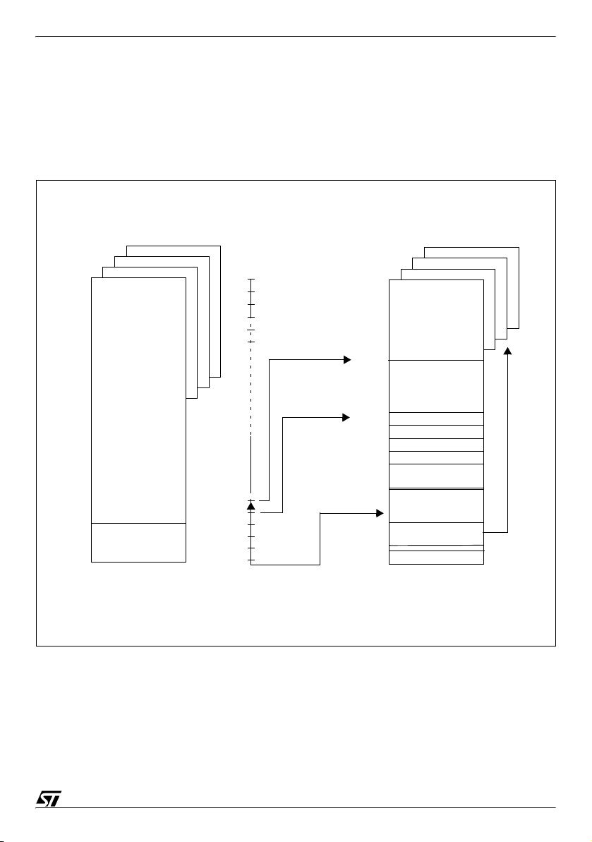
1.3 MEMORY MAP
1.3.1 Introduction
The MCU operates in three separate memory
spaces: Program space, Data space, and Stack
space. Operation in these three memory spaces is
described in the following paragraphs.
Figure 3Memory Addressing Diagram
Briefly, Program space contains user program
code in OTP and user vectors; Data space con
tains user data in RAM and in OTP, and Stack
space accommodates six levels of stack for sub
routine and interrupt service routine nesting.
-
-
6/83

ST6253C ST6263C ST6263B ST6260C ST6260B
0000h
RESERVED
*
USER
PROGRAM MEMORY
(OTP/EPROM)
3872 BYTES
0F9Fh
0FA0h
0FEFh
0FF0h
0FF7h
0FF8h
0FFBh
0FFCh
0FFDh
0FFEh
0FFFh
RESERVED
*
RESERVED
INTERRUPT VECTORS
NMI VECTOR
USER RESET VECTOR
0080h
(*) Reserved areas should be filled with 0FFh
007Fh
0000h
RESERVED
*
USER
PROGRAM MEMORY
(OTP)
1824 BYTES
0F9Fh
0FA0h
0FEFh
0FF0h
0FF7h
0FF8h
0FFBh
0FFCh
0FFDh
0FFEh
0FFFh
RESERVED
*
RESERVED
INTERRUPT VECTORS
NMI VECTOR
USER RESET VECTOR
087Fh
(*) Reserved areas should be filled with 0FFh
0880h
MEMORY MAP (Cont’d)
1.3.2 Program Space
Program Space comprises the instructions to be
executed, the data required for immediate ad
dressing mode instructions, the reserved factory
test area and the user vectors. Program Space is
addressed via the 12-bit Program Counter register
(PC register).
1.3.2.1 Program Memory Protection
The Program Memory in OTP or EPROM devices
can be protected against external readout of mem
ory by selecting the READOUT PROTECTION option in the option byte.
Figure 4ST62E60C/T60C Program
Memory Map
In the EPROM parts, READOUT PROTECTION
-
option can be disactivated only by U.V. erasure
that also results into the whole EPROM context
erasure.
Note: Once the Readout Protection is activated, it
is no longer possible, even for STMicroelectronics,
to gain access to the OTP contents. Returned
parts with a protection set can therefore not be ac
cepted.
-
Figure 5ST62T53C/T63C Program
Memory Map
-
7/83
ST6253C ST6263C ST6263B ST6260C ST6260B
MEMORY MAP (Cont’d)
1.3.3 Data Space
Data Space accommodates all the data necessary
for processing the user program. This space com
prises the RAM resource, the processor core and
peripheral registers, as well as read-only data
such as constants and look-up tables in OTP/
EPROM.
1.3.3.1 Data ROM
All read-only data is physically stored in program
memory, which also accommodates the Program
Space. The program memory consequently con
tains the program code to be executed, as well as
the constants and look-up tables required by the
application.
The Data Space locations in which the different
constants and look-up tables are addressed by the
processor core may be thought of as a 64-byte
window through which it is possible to access the
read-only data stored in OTP/EPROM.
1.3.3.2 Data RAM/EEPROM
In ST62T53C, T60C, T63C and ST62E60C devices, the data space includes 60 bytes of RAM, the
accumulator (A), the indirect registers (X), (Y), the
short direct registers (V), (W), the I/O port regis
ters, the peripheral data and control registers, the
interrupt option register and the Data ROM Win
dow register (DRW register).
Additional RAM and EEPROM pages can also be
addressed using banks of 64 bytes located be
tween addresses 00h and 3Fh.
1.3.4 Stack Space
Stack space consists of six 12-bit registers which
are used to stack subroutine and interrupt return
addresses, as well as the current program counter
contents.
Table 1. Additional RAM/EEPROM Banks
Device RAM EEPROM
ST62T53C 1 x 64 bytes -
ST62T60C/E60C 1 x 64 bytes 2 x 64 bytes
ST62T63C 1 x 64 bytes 1 x 64 bytes
Table 2ST62T53C, T60C, T63C and ST62E60C
Data Memory Space
-
-
-
-
-
AR TIMER STATUS/CONTROL REGISTER1 0D6h
AR TIMER STATUS/CONTROL REGISTER2 0D7h
AR TIMER RELOAD/CAPTURE REGISTER 0D9h
* WRITE ONLY REGISTER
RAM and EEPROM
DATA ROM WINDOW AREA
X REGISTER 080h
Y REGISTER 081h
V REGISTER 082h
W REGISTER 083h
DATA RAM 60 BYTES
PORT A DATA REGISTER 0C0h
PORT B DATA REGISTER 0C1h
PORT C DATA REGISTER 0C2h
RESERVED 0C3h
PORT A DIRECTION REGISTER 0C4h
PORT B DIRECTION REGISTER 0C5h
PORT C DIRECTION REGISTER 0C6h
RESERVED 0C7h
INTERRUPT OPTION REGISTER 0C8h*
DATA ROM WINDOW REGISTER 0C9h*
RESERVED
PORT A OPTION REGISTER 0CCh
PORT B OPTION REGISTER 0CDh
PORT C OPTION REGISTER 0CEh
RESERVED 0CFh
A/D DATA REGISTER 0D0h
A/D CONTROL REGISTER 0D1h
TIMER PRESCALER REGISTER 0D2h
TIMER COUNTER REGISTER 0D3h
TIMER STATUS CONTROL REGISTER 0D4h
AR TIMER MODE CONTROL REGISTER 0D5h
WATCHDOG REGISTER 0D8h
AR TIMER COMPARE REGISTER 0DAh
AR TIMER LOAD REGISTER 0DBh
OSCILLATOR CONTROL REGISTER 0DCh*
MISCELLANEOUS 0DDh
RESERVED
SPI DATA REGISTER 0E0h
SPI DIVIDER REGISTER 0E1h
SPI MODE REGISTER 0E2h
RESERVED
DATA RAM/EEPROM REGISTER 0E8h*
RESERVED 0E9h
EEPROM CONTROL REGISTER
(except ST62T53C)
RESERVED
ACCUMULATOR 0FFh
000h
03Fh
040h
07Fh
084h
0BFh
0CAh
0CBh
0DEh
0DFh
0E3h
0E7h
0EAh
0EBh
0FEh
8/83
ST6253C ST6263C ST6263B ST6260C ST6260B
DATA ROM
WINDOW REGISTER
CONTENTS
DATA SPACE ADDRESS
40h-7Fh
IN INSTRUCTION
PROGRAM SPACE ADDRESS
765432 0
543210
543210
READ
1
67891011
0
1
VR01573C
12
1
0
DATA SPACE ADDRESS
:
:
59h
000
0
1
00
1
11
Example:
(DWR)
DWR=28h
11
0000000
1
ROM
ADDRESS:A19h
11
13
0
1
MEMORY MAP (Cont’d)
1.3.5 Data Window Register (DWR)
The Data read-only memory window is located from
address 0040h to address 007Fh in Data space. It
allows direct reading of 64 consecutive bytes locat
ed anywhere in program memory, between address 0000h and 0FFFh (top memory address depends on the specific device). All the program
memory can therefore be used to store either in
structions or read-only data. Indeed, the window
can be moved in steps of 64 bytes along the pro
gram memory by writing the appropriate code in the
Data Window Register (DWR).
The DWR can be addressed like any RAM location
in the Data Space, it is however a write-only regis
ter and therefore cannot be accessed using singlebit operations. This register is used to position the
64-byte read-only data window (from address 40h
to address 7Fh of the Data space) in program
memory in 64-byte steps. The effective address of
the byte to be read as data in program memory is
obtained by concatenating the 6 least significant
bits of the register address given in the instruction
(as least significant bits) and the content of the
DWR register (as most significant bits), as illustrat
ed in Figure 6 below. For instance, when addressing location 0040h of the Data Space, with 0 loaded in the DWR register, the physical location addressed in program memory is 00h. The DWR register is not cleared on reset, therefore it must be
written to prior to the first access to the Data readonly memory window area.
Figure 6Data read-only memory Window Memory Addressing
Data Window Register (DWR)
Address: 0C9h — Write Only
7 0
-
- - DWR5 DWR4 DWR3 DWR2 DWR1 DWR0
Bits 6, 7 = Not used.
Bit 5-0 = DWR6-DWR0: Data read-only memory
Window Register Bits. These are the Data read-
only memory Window bits that correspond to the
upper bits of the data read-only memory space.
Caution: This register is undefined on reset. Nei-
-
ther read nor single bit instructions may be used to
address this register.
Note: Care is required when handling the DWR
register as it is write only. For this reason, the
DWR contents should not be changed while exe
cuting an interrupt service routine, as the service
routine cannot save and then restore the register’s
previous contents. If it is impossible to avoid writ
ing to the DWR during the interrupt service routine,
-
an image of the register must be saved in a RAM
location, and each time the program writes to the
DWR, it must also write to the image register. The
image register must be written first so that, if an in
terrupt occurs between the two instructions, the
DWR is not affected.
-
-
-
9/83

ST6253C ST6263C ST6263B ST6260C ST6260B
MEMORY MAP (Cont’d)
1.3.6 Data RAM/EEPROM Bank Register (DRBR)
Address: E8h — Write only
7 0
- - -
DRBR
4
- -
DRBR1DRBR
Bit 7-5 = These bits are not used
Bit 4 - DRBR4. This bit, when set, selects RAM
Page 2.
Bit 3-2 - Reserved. These bits are not used.
Bit 1 - DRBR1. This bit, when set, selects
EEPROM Page 1, when available.
Bit 0 - DRBR0. This bit, when set, selects
EEPROM Page 0, when available.
The selection of the bank is made by programming
the Data RAM Bank Switch register (DRBR regis
ter) located at address E8h of the Data Space according to Table 1. No more than one bank should
be set at a time.
The DRBR register can be addressed like a RAM
Data Space at the address E8h; nevertheless it is
a write only register that cannot be accessed with
single-bit operations. This register is used to select
the desired 64-byte RAM/EEPROM bank of the
Data Space. The bank number has to be loaded in
the DRBR register and the instruction has to point
Table 3Data RAM Bank Register Set-up
DRBR ST62T53C ST62T60C/E60C ST62T63C
to the selected location as if it was in bank 0 (from
00h address to 3Fh address).
This register is not cleared during the MCU initialization, therefore it must be written before the first
access to the Data Space bank region. Refer to
the Data Space description for additional informa
0
tion. The DRBR register is not modified when an
interrupt or a subroutine occurs.
Notes :
Care is required when handling the DRBR register
as it is write only. For this reason, it is not allowed
to change the DRBR contents while executing in
terrupt service routine, as the service routine cannot save and then restore its previous content. If it
is impossible to avoid the writing of this register in
interrupt service routine, an image of this register
must be saved in a RAM location, and each time
the program writes to DRBR it must write also to
the image register. The image register must be
-
written first, so if an interrupt occurs between the
two instructions the DRBR is not affected.
In DRBR Register, only 1 bit must be set. Otherwise two or more pages are enabled in parallel,
producing errors.
Care must also be taken not to change the
E²PROM page (when available) when the parallel
writing mode is set for the E²PROM, as defined in
EECTL register.
-
-
00 None None None
01 Not Available EEPROM Page 0 EEPROM Page 0
02 Not Available EEPROM Page 1 Not Available
08 Not Available Not Available Not Available
10h RAM Page 2 RAM Page 2 RAM Page 2
other Reserved Reserved Reserved
10/83

ST6253C ST6263C ST6263B ST6260C ST6260B
MEMORY MAP (Cont’d)
1.3.7 EEPROM Description
EEPROM memory is located in 64-byte pages in
data space. This memory may be used by the user
program for non-volatile data storage.
Data space from 00h to 3Fh is paged as described
in Table 4. EEPROM locations are accessed di
rectly by addressing these paged sections of data
space.
The EEPROM does not require dedicated instructions for read or write access. Once selected via the
Data RAM Bank Register, the active EEPROM
page is controlled by the EEPROM Control Regis
ter (EECTL), which is described below.
Bit E20FF of the EECTL register must be reset prior
to any write or read access to the EEPROM. If no
bank has been selected, or if E2OFF is set, any ac
cess is meaningless.
Programming must be enabled by setting the
E2ENA bit of the EECTL register.
The E2BUSY bit of the EECTL register is set when
the EEPROM is performing a programming cycle.
Any access to the EEPROM when E2BUSY is set
is meaningless.
Provided E2OFF and E2BUSY are reset, an EEPROM location is read just like any other data location, also in terms of access time.
Writing to the EEPROM may be carried out in two
modes: Byte Mode (BMODE) and Parallel Mode
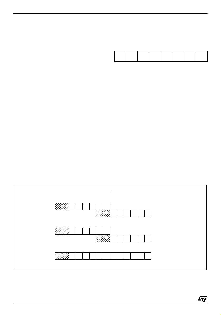
Table 4. Row Arrangement for Parallel Writing of EEPROM Locations
Byte 0 1 2 3 4 5 6 7
ROW7 38h-3Fh
ROW6 30h-37h
ROW5 28h-2Fh
ROW4 20h-27h
ROW3 18h-1Fh
ROW2 10h-17h
ROW1 08h-0Fh
ROW0 00h-07h
(PMODE). In BMODE, one byte is accessed at a
time, while in PMODE up to 8 bytes in the same
row are programmed simultaneously (with conse
quent speed and power consumption advantages,
the latter being particularly important in battery
powered circuits).
General Notes:
Data should be written directly to the intended address in EEPROM space. There is no buffer memory between data RAM and the EEPROM space.
When the EEPROM is busy (E2BUSY = “1”)
-
EECTL cannot be accessed in write mode, it is
only possible to read the status of E2BUSY. This
implies that as long as the EEPROM is busy, it is
not possible to change the status of the EEPROM
Control Register. EECTL bits 4 and 5 are reserved
and must never be set.
Care is required when dealing with the EECTL register, as some bits are write only. For this reason,
the EECTL contents must not be altered while ex
ecuting an interrupt service routine.
If it is impossible to avoid writing to this register
within an interrupt service routine, an image of the
register must be saved in a RAM location, and
each time the program writes to EECTL it must
also write to the image register. The image register
must be written to first so that, if an interrupt oc
curs between the two instructions, the EECTL will
not be affected.
Dataspace
addresses.
Banks 0 and 1.
-
-
-
Up to 8 bytes in each row may be programmed simultaneously in Parallel Write mode.
The number of available 64-byte banks (1 or 2) is device dependent.
Note: The EEPROM is disabled as soon as STOP instruction is executed in order to achieve the lowest
power-consumption.
11/83

ST6253C ST6263C ST6263B ST6260C ST6260B
MEMORY MAP (Cont’d)
Additional Notes on Parallel Mode:
If the user wishes to perform parallel programming, the first step should be to set the E2PAR2
bit. From this time on, the EEPROM will be ad
dressed in write mode, the ROW address and the
data will be latched and it will be possible to
change them only at the end of the programming
cycle or by resetting E2PAR2 without program
ming the EEPROM. After the ROW address is
latched, the MCU can only “see” the selected
EEPROM row and any attempt to write or read
other rows will produce errors.
The EEPROM should not be read while E2PAR2
is set.
As soon as the E2PAR2 bit is set, the 8 volatile
ROW latches are cleared. From this moment on,
the user can load data in all or in part of the ROW.
Setting E2PAR1 will modify the EEPROM regis
ters corresponding to the ROW latches accessed
after E2PAR2. For example, if the software sets
E2PAR2 and accesses the EEPROM by writing to
addresses 18h, 1Ah and 1Bh, and then sets
E2PAR1, these three registers will be modified si
multaneously; the remaining bytes in the row will
be unaffected.
Note that E2PAR2 is internally reset at the end of
the programming cycle. This implies that the user
must set the E2PAR2 bit between two parallel pro
gramming cycles. Note that if the user tries to set
E2PAR1 while E2PAR2 is not set, there will be no
programming cycle and the E2PAR1 bit will be un
affected. Consequently, the E2PAR1 bit cannot be
set if E2ENA is low. The E2PAR1 bit can be set by
the user, only if the E2ENA and E2PAR2 bits are
also set.
Notes: The EEPROM page shall not be changed
through the DRBR register when the E2PAR2 bit
is set.
EEPROM Control Register (EECTL)
Address: EAh — Read/Write
Reset status: 00h
-
7 0
E2O
D7
-
FF
D5 D4
E2PAR1E2PAR2E2BUSYE2E
Bit 7 = D7: Unused.
Bit 6 = E2OFF: Stand-by Enable Bit. WRITE ONLY.
If this bit is set the EEPROM is disabled (any access
will be meaningless) and the power consumption of
the EEPROM is reduced to its lowest value.
Bit 5-4 = D5-D4: Reserved. MUST be kept reset.
Bit 3 = E2PAR1: Parallel Start Bit. WRITE ONLY.
Once in Parallel Mode, as soon as the user software
-
sets the E2PAR1 bit, parallel writing of the 8 adja
cent registers will start. This bit is internally reset at
the end of the programming procedure. Note that
less than 8 bytes can be written if required, the un
defined bytes being unaffected by the parallel pro-
-
gramming cycle; this is explained in greater detail in
the Additional Notes on Parallel Mode overleaf.
Bit 2 = E2PAR2: Parallel Mode En. Bit. WRITE
ONLY. This bit must be set by the user program in
order to perform parallel programming. If E2PAR2
-
is set and the parallel start bit (E2PAR1) is reset,
up to 8 adjacent bytes can be written simultane
ously. These 8 adjacent bytes are considered as a
-
row, whose address lines A7, A6, A5, A4, A3 are
fixed while A2, A1 and A0 are the changing bits, as
illustrated in
Table 4. E2PAR2 is automatically re-
set at the end of any parallel programming procedure. It can be reset by the user software before
starting the programming procedure, thus leaving
the EEPROM registers unchanged.
Bit 1 = E2BUSY: EEPROM Busy Bit. READ ON-
LY. This bit is automatically set by the EEPROM
control logic when the EEPROM is in program
ming mode. The user program should test it before
any EEPROM read or write operation; any attempt
to access the EEPROM while the busy bit is set
will be aborted and the writing procedure in
progress will be completed.
Bit 0 = E2ENA: EEPROM Enable Bit. WRITE ON-
LY. This bit enables programming of the EEPROM
cells. It must be set before any write to the EEP
ROM register. Any attempt to write to the EEPROM when E2ENA is low is meaningless and will
not trigger a write cycle.
The EEPROM is disabled as soon as a STOP instruction is executed in order to achieve the lowest
power-consumption.
NA
-
-
-
-
-
12/83

ST6253C ST6263C ST6263B ST6260C ST6260B
1.4 PROGRAMMING MODES
1.4.1 Option Bytes
The two Option Bytes allow configuration capability to the MCUs. Option byte’s content is automatically read, and the selected options enabled, when
the chip reset is activated.
It can only be accessed during the programming
mode. This access is made either automatically
(copy from a master device) or by selecting the
OPTION BYTE PROGRAMMING mode of the pro
grammer.
The option bytes are located in a non-user map.
No address has to be specified.
EPROM Code Option Byte (LSB)
7 0
PRO-
EXTC-
PB2-3
TECT
NTL
PULL
PB0-1
PULL
WDACT
DELAY
OSCIL OSGEN
EPROM Code Option Byte (MSB)
15 8
- - -
ADC
SYNCHRO
- -
NMI
PULL
D15-D13. Reserved. Must be cleared.
ADC SYNCHRO. When set, an A/D conversion is
started upon WAIT instruction execution, in order
to reduce supply noise. When this bit is low, an A/
D conversion is started as soon as the STA bit of
the A/D Converter Control Register is set.
D11. Reserved, must be set to one.
D10. Reserved, must be cleared.
NMI PULL. NMI Pull-Up. This bit must be set high
to configure the NMI pin with a pull-up resistor.
When it is low, no pull-up is provided.
LVD. LVD RESET enable.When this bit is set, safe
RESET is performed by MCU when the supply
-
LVD
voltage is too low. When this bit is cleared, only
power-on reset or external RESET are active.
PROTECT. Readout Protection. This bit allows the
protection of the software contents against piracy.
When the bit PROTECT is set high, readout of the
OTP contents is prevented by hardware.. When
this bit is low, the user program can be read.
EXTCNTL. External STOP MODE control.. When
EXTCNTL is high, STOP mode is available with
watchdog active by setting NMI pin to one. When
EXTCNTL is low, STOP mode is not available with
the watchdog active.
PB2-3 PULL. When set this bit removes pull-up at
reset on PB2-PB3 pins. When cleared PB2-PB3
pins have an internal pull-up resistor at reset.
PB0-1 PULL. When set this bit removes pull-up at
reset on PB0-PB1 pins. When cleared PB0-PB1
pins have an internal pull-up resistor at reset.
WDACT. This bit controls the watchdog activation.
When it is high, hardware activation is selected.
The software activation is selected when WDACT
is low.
DELAY. This bit enables the selection of the delay
internally generated after the internal reset (exter
nal pin, LVD, or watchdog activated) is released.
When DELAY is low, the delay is 2048 cycles of
the oscillator, it is of 32768 cycles when DELAY is
high.
OSCIL. Oscillator selection. When this bit is low,
the oscillator must be controlled by a quartz crys
tal, a ceramic resonator or an external frequency.
When it is high, the oscillator must be controlled by
an RC network, with only the resistor having to be
externally provided.
OSGEN. Oscillator Safe Guard. This bit must be
set high to enable the Oscillator Safe Guard.
When this bit is low, the OSG is disabled.
The Option byte is written during programming either by using the PC menu (PC driven Mode) or
automatically (stand-alone mode).
-
-
13/83

ST6253C ST6263C ST6263B ST6260C ST6260B
PROGRAMMING MODES (Cont’d)
1.4.2 EPROM Erasing
The EPROM of the windowed package of the
MCUs may be erased by exposure to Ultra Violet
light. The erasure characteristic of the MCUs is
such that erasure begins when the memory is ex
posed to light with a wave lengths shorter than approximately 4000Å. It should be noted that sunlights and some types of fluorescent lamps have
wavelengths in the range 3000-4000Å.
It is thus recommended that the window of the
MCUs packages be covered by an opaque label to
prevent unintentional erasure problems when test
ing the application in such an environment.
The recommended erasure procedure of the
MCUs EPROM is the exposure to short wave ul
-
traviolet light which have a wave-length 2537A.
The integrated dose (i.e. U.V. intensity x exposure
time) for erasure should be a minimum of 15W-
2
. The erasure time with this dosage is ap-
sec/cm
proximately 15 to 20 minutes using an ultraviolet
lamp with 12000µW/cm
2
power rating. The
ST62E60C should be placed within 2.5cm (1Inch)
of the lamp tubes during erasure.
-
-
14/83

ST6253C ST6263C ST6263B ST6260C ST6260B
PROGRAM
RESET
OPCODE
FLAG
VALUES
2
CONTROLLER
FLAGS
ALU
A-DATA
B-DATA
ADDRESS/READ LINE
DATA SPACE
INTERRUPTS
DATA
RAM/EEPROM
DATA
ROM/EPROM
RESULTS TO DATA SPACE (WRITE LINE)
ROM/EPROM
DEDICATIONS
ACCUMULATOR
CONTROL
SIGNALS
OSCin
OSCout
ADDRESS
DECODER
256
12
Program Counter
and
6 LAYER STACK
0,01 TO 8MHz
VR01811
2 CENTRAL PROCESSING UNIT
2.1 INTRODUCTION
The CPU Core of ST6 devices is independent of the
I/O or Memory configuration. As such, it may be
thought of as an independent central processor
communicating with on-chip I/O, Memory and Pe
ripherals via internal address, data, and control
buses. In-core communication is arranged as
shown in Figure 7; the controller being externally
linked to both the Reset and Oscillator circuits,
while the core is linked to the dedicated on-chip pe
ripherals via the serial data bus and indirectly, for
interrupt purposes, through the control registers.
2.2 CPU REGISTERS
The ST6 Family CPU core features six registers and
three pairs of flags available to the programmer.
These are described in the following paragraphs.
Accumulator (A). The accumulator is an 8-bit
general purpose register used in all arithmetic cal
culations, logical operations, and data manipulations. The accumulator can be addressed in Data
space as a RAM location at address FFh. Thus the
ST6 can manipulate the accumulator just like any
other register in Data space.
Figure 7. ST6 Core Block Diagram
-
-
-
Indirect Registers (X, Y). These two indirect registers are used as pointers to memory locations in
Data space. They are used in the register-indirect
addressing mode. These registers can be ad
dressed in the data space as RAM locations at addresses 80h (X) and 81h (Y). They can also be accessed with the direct, short direct, or bit direct addressing modes. Accordingly, the ST6 instruction
set can use the indirect registers as any other reg
ister of the data space.
Short Direct Registers (V, W). These two registers are used to save a byte in short direct addressing mode. They can be addressed in Data
space as RAM locations at addresses 82h (V) and
83h (W). They can also be accessed using the di
rect and bit direct addressing modes. Thus, the
ST6 instruction set can use the short direct regis
ters as any other register of the data space.
Program Counter (PC). The program counter is a
12-bit register which contains the address of the
next ROM location to be processed by the core.
This ROM location may be an opcode, an oper
and, or the address of an operand. The 12-bit
length allows the direct addressing of 4096 bytes
in Program space.
-
-
-
-
-
15/83
CPU REGISTERS (Cont’d)
SHORT
DIRECT
ADDRESSING
MODE
VREGISTER
WREGISTER
PROGRAM COUNTER
SIX LEVELS
STACK REGISTER
CZNORMAL FLAGS
INTERRUPT FLAGS
NMI FLAGS
INDEX
REGISTER
VA000423
b7
b7
b7
b7
b7
b0
b0
b0
b0
b0
b0b11
ACCUMULATOR
Y REG. POINTER
X REG. POINTER
CZ
CZ
However, if the program space contains more than
4096 bytes, the additional memory in program
space can be addressed by using the Program
Bank Switch register.
The PC value is incremented after reading the address of the current instruction. To execute relative
jumps, the PC and the offset are shifted through
the ALU, where they are added; the result is then
shifted back into the PC. The program counter can
be changed in the following ways:
- JP (Jump) instructionPC=Jump address
- CALL instructionPC= Call address
- Relative Branch Instruction.PC= PC +/- offset
- Interrupt PC=Interrupt vector
- Reset PC= Reset vector
- RET & RETI instructionsPC= Pop (stack)
- Normal instructionPC= PC + 1
Flags (C, Z). The ST6 CPU includes three pairs of
flags (Carry and Zero), each pair being associated
with one of the three normal modes of operation:
Normal mode, Interrupt mode and Non Maskable
Interrupt mode. Each pair consists of a CARRY
flag and a ZERO flag. One pair (CN, ZN) is used
during Normal operation, another pair is used dur
ing Interrupt mode (CI, ZI), and a third pair is used
in the Non Maskable Interrupt mode (CNMI, ZN
MI).
The ST6 CPU uses the pair of flags associated
with the current mode: as soon as an interrupt (or
a Non Maskable Interrupt) is generated, the ST6
CPU uses the Interrupt flags (resp. the NMI flags)
instead of the Normal flags. When the RETI in
struction is executed, the previously used set of
flags is restored. It should be noted that each flag
set can only be addressed in its own context (Non
Maskable Interrupt, Normal Interrupt or Main rou
tine). The flags are not cleared during context
switching and thus retain their status.
The Carry flag is set when a carry or a borrow occurs during arithmetic operations; otherwise it is
cleared. The Carry flag is also set to the value of
the bit tested in a bit test instruction; it also partici
pates in the rotate left instruction.
The Zero flag is set if the result of the last arithmetic or logical operation was equal to zero; otherwise it is cleared.
Switching between the three sets of flags is performed automatically when an NMI, an interrupt or
a RETI instructions occurs. As the NMI mode is
ST6253C ST6263C ST6263B ST6260C ST6260B
automatically selected after the reset of the MCU,
the ST6 core uses at first the NMI flags.
Stack. The ST6 CPU includes a true LIFO hardware stack which eliminates the need for a stack
pointer. The stack consists of six separate 12-bit
RAM locations that do not belong to the data
space RAM area. When a subroutine call (or inter
rupt request) occurs, the contents of each level are
shifted into the next higher level, while the content
of the PC is shifted into the first level (the original
contents of the sixth stack level are lost). When a
subroutine or interrupt return occurs (RET or RETI
instructions), the first level register is shifted back
into the PC and the value of each level is popped
back into the previous level. Since the accumula
tor, in common with all other data space registers,
is not stored in this stack, management of these
registers should be performed within the subrou
tine. The stack will remain in its “deepest” position
if more than 6 nested calls or interrupts are execut
ed, and consequently the last return address will
be lost. It will also remain in its highest position if
the stack is empty and a RET or RETI is executed.
In this case the next instruction will be executed.
Figure 8. ST6 CPU Programming Mode
l
-
-
-
-
-
-
-
-
-
16/83
ST6253C ST6263C ST6263B ST6260C ST6260B
INTEGRATED CLOCK
CRYSTAL/RESONATOR option
OSG ENABLED option
OSC
in
OSC
out
C
L1n
C
L2
ST6xxx
CRYSTAL/RESONATOR CLOCK
CRYSTAL/RESONATOR option
OSC
in
OSC
out
ST6xxx
EXTERNAL CLOCK
CRYSTAL/RESONATOR option
NC
OSC
in
OSC
out
ST6xxx
NC
OSC
in
OSC
out
R
NET
ST6xxx
RC NETWORK
RC NETWORK option
NC
3 CLOCKS, RESET, INTERRUPTS AND POWER SAVING MODES
3.1 CLOCK SYSTEM
The MCU features a Main Oscillator which can be
driven by an external clock, or used in conjunction
with an AT-cut parallel resonant crystal or a suita
ble ceramic resonator, or with an external resistor
). In addition, a Low Frequency Auxiliary Os-
(R
NET
cillator (LFAO) can be switched in for security reasons, to reduce power consumption, or to offer the
benefits of a back-up clock system.
The Oscillator Safeguard (OSG) option filters
spikes from the oscillator lines, provides access to
the LFAO to provide a backup oscillator in the
event of main oscillator failure and also automati
cally limits the internal clock frequency (f
function of V
ation. These functions are illustrated in Figure 10,
Figure 11, Figure 12 and Figure 13.
A programmable divider on F
order to adjust the internal clock of the MCU to the
, in order to guarantee correct oper-
DD
is also provided in
INT
INT
) as a
best power consumption and performance tradeoff.
Figure 9 illustrates various possible oscillator con-
figurations using an external crystal or ceramic resonator, an external clock input, an external resistor
(R
LFAO. C
range 12 to 22 pF for an oscillator frequency in the
4-8 MHz range.
The internal MCU clock frequency (f
by 12 to drive the Timer, the A/D converter and the
Watchdog timer, and by 13 to drive the CPU core,
as may be seen in Figure 12.
), or the lowest cost solution using only the
NET
an CL2 should have a capacitance in the
L1
) is divided
INT
With an 8 MHz oscillator frequency, the fastest machine cycle is therefore 1.625µs.
A machine cycle is the smallest unit of time needed
to execute any operation (for instance, to increment
the Program Counter). An instruction may require
two, four, or five machine cycles for execution.
3.1.1 Main Oscillator
The oscillator configuration may be specified by selecting the appropriate option. When the CRYSTAL/
RESONATOR option is selected, it must be used with
a quartz crystal, a ceramic resonator or an external
signal provided on the OSCin pin. When the RC NET
WORK option is selected, the system clock is generated by an external resistor.
The main oscillator can be turned off (when the
OSG ENABLED option is selected) by setting the
OSCOFF bit of the ADC Control Register. The
Low Frequency Auxiliary Oscillator is automatical
ly started.
Figure 9. Oscillator Configurations
-
-
-
-
17/83

ST6253C ST6263C ST6263B ST6260C ST6260B
CLOCK SYSTEM (Cont’d)
Turning on the main oscillator is achieved by resetting the OSCOFF bit of the A/D Converter Control Register or by resetting the MCU. Restarting
the main oscillator implies a delay comprising the
oscillator start up delay period plus the duration of
the software instruction at f
3.1.2 Low Frequency Auxiliary Oscillator (LFAO)
The Low Frequency Auxiliary Oscillator has three
main purposes. Firstly, it can be used to reduce
power consumption in non timing critical routines.
Secondly, it offers a fully integrated system clock,
without any external components. Lastly, it acts as
a safety oscillator in case of main oscillator failure.
This oscillator is available when the OSG ENABLED option is selected. In this case, it automatically starts one of its periods after the first missing
edge from the main oscillator, whatever the reason
(main oscillator defective, no clock circuitry provid
ed, main oscillator switched off...).
User code, normal interrupts, WAIT and STOP instructions, are processed as normal, at the reduced f
cy is decreased, since the internal frequency is be-
frequency. The A/D converter accura-
LFAO
low 1MHz.
At power on, the Low Frequency Auxiliary Oscilla-
tor starts faster than the Main Oscillator. It therefore feeds the on-chip counter generating the POR
delay until the Main Oscillator runs.
The Low Frequency Auxiliary Oscillator is automatically switched off as soon as the main oscillator starts.
ADCR
Address: 0D1h — Read/Write
7 0
ADCR7ADCR6ADCR5ADCR4ADCR3OSC
Bit 7-3, 1-0= ADCR7-ADCR3, ADCR1-ADCR0:
ADC Control Register. These bits are reserved for
ADC Control.
Bit 2 = OSCOFF. When low, this bit enables main
oscillator to run. The main oscillator is switched off
when OSCOFF is high.
3.1.3 Oscillator Safe Guard
The Oscillator Safe Guard (OSG) affords drastically increased operational integrity in ST62xx devices. The OSG circuit provides three basic func-
clock frequency.
LFAO
OFF
ADCR1ADCR
0
-
tions: it filters spikes from the oscillator lines which
would result in over frequency to the ST62 CPU; it
gives access to the Low Frequency Auxiliary Os
cillator (LFAO), used to ensure minimum processing in case of main oscillator failure, to offer reduced power consumption or to provide a fixed frequency low cost oscillator; finally, it automatically
limits the internal clock frequency as a function of
supply voltage, in order to ensure correct opera
tion even if the power supply should drop.
The OSG is enabled or disabled by choosing the
relevant OSG option. It may be viewed as a filter
whose cross-over frequency is device dependent.
Spikes on the oscillator lines result in an effectively
increased internal clock frequency. In the absence
of an OSG circuit, this may lead to an over fre
quency for a given power supply voltage. The
OSG filters out such spikes (as illustrated in Figure
10). In all cases, when the OSG is active, the max
imum internal clock frequency, f
, which is supply voltage dependent. This re-
f
OSG
lationship is illustrated in Figure 13.
, is limited to
INT
When the OSG is enabled, the Low Frequency
Auxiliary Oscillator may be accessed. This oscilla
tor starts operating after the first missing edge of
the main oscillator (see Figure 11).
Over-frequency, at a given power supply level, is
seen by the OSG as spikes; it therefore filters out
some cycles in order that the internal clock fre
quency of the device is kept within the range the
particular device can stand (depending on V
and below f
cy with OSG enabled.
: the maximum authorised frequen-
OSG
DD
),
Note. The OSG should be used wherever possible
as it provides maximum safety. Care must be tak
en, however, as it can increase power consumption and reduce the maximum operating frequency
.
to f
OSG
Warning: Care has to be taken when using the
OSG, as the internal frequency is defined between
a minimum and a maximum value and is not accu
rate.
For precise timing measurements, it is not recommended to use the OSG and it should not be enabled in applications that use the SPI or the UART.
It should also be noted that power consumption in
Stop mode is higher when the OSG is enabled
(around 50µA at nominal conditions and room
temperature).
-
-
-
-
-
-
-
-
18/83
ST6253C ST6263C ST6263B ST6260C ST6260B
(1)
VR001932
(3)
(2)
(4)
(1)
(2)
(3)
(4)
Maximum Frequency for the device to work correctly
Actual Quartz Crystal Frequency at OSCin pin
Noise from OSCin
Resulting Internal Frequency
Main
VR001933
Internal
Emergency
Oscillator
Frequency
Oscillator
CLOCK SYSTEM (Cont’d)
Figure 10. OSG Filtering Principle
Figure 11. OSG Emergency Oscillator Principle
19/83

ST6253C ST6263C ST6263B ST6260C ST6260B
CLOCK SYSTEM (Cont’d)
Oscillator Control Registers
Address: DCh — Write only
Reset State: 00h
7 0
- - - -
Bit 7-4. These bits are not used.
Bit 3. Reserved. Cleared at Reset. Must be kept
cleared.
Bit 2. Reserved. Must be kept low.
RS1-RS0. These bits select the division ratio of
the Oscillator Divider in order to generate the inter
nal frequency. The following selctions are available:
OSCR
3
- RS1 RS0
RS1 RS0 Division Ratio
0
0
1
1
0
1
0
1
Note: Care is required when handling the OSCR
register as some bits are write only. For this rea
son, it is not allowed to change the OSCR contents
while executing interrupt service routine, as the
service routine cannot save and then restore its
previous content. If it is impossible to avoid the
writing of this register in interrupt service routine,
an image of this register must be saved in a RAM
location, and each time the program writes to
-
OSCR it must write also to the image register. The
image register must be written first, so if an inter
rupt occurs between the two instructions the
OSCR is not affected.
1
2
4
4
-
-
20/83
ST6253C ST6263C ST6263B ST6260C ST6260B
MAIN
OSCILLATOR
OSG
LFAO
M
U
X
Core
: 13
:
12
:
1
TIMER 1
Watchdog
POR
f
INT
Main Oscillator off
OSCILLATOR
DIVIDER
RS0,RS1
1
2.5
3.644.555.56
8
7
6
5
4
3
2
Maximum FREQUENCY (MHz)
SUPPLY VOLTAGE (V
DD
)
FUNCTIONALITY IS NOT
3
4
3
2
1
f
OSG
f
OSG
Min (at 85°C)
GUARANTEED
IN THIS AREA
VR01807J
f
OSG
Min (at 125°C)
CLOCK SYSTEM (Cont’d)
Figure 12. Clock Circuit Block Diagram
Figure 13. Maximum Operating Frequency (f
Notes:
1. In this area, operation is guaranteed at the
quartz crystal frequency.
2. When the OSG is disabled, operation in this
area is guaranteed at the crystal frequency. When
the OSG is enabled, operation in this area is guaranteed at a frequency of at least f
3. When the OSG is disabled, operation in this
OSG Min.
MAX
21/83
) versus Supply Voltage (VDD)
area is guaranteed at the quartz crystal frequency.
When the OSG is enabled, access to this area is
prevented. The internal frequency is kept a f
4. When the OSG is disabled, operation in this
area is not guaranteed
When the OSG is enabled, access to this area is
prevented. The internal frequency is kept at f
OSG.
OSG.
ST6253C ST6263C ST6263B ST6260C ST6260B
INT LATCH CLEARED
NMI MASK SET
RESET
( IF PRESENT )
SELECT
NMI MODE FLAGS
IS RESET STILL
PRESENT?
YES
PUT FFEH
ON ADDRESS BUS
FROM RESET LOCATIONS
FFE/FFF
NO
FETCH INSTRUCTION
LOAD PC
VA000427
3.2 RESETS
The MCU can be reset in four ways:
– by the external Reset input being pulled low;
– by Power-on Reset;
– by the digital Watchdog peripheral timing out.
– by Low Voltage Detection (LVD)
3.2.1 RESET Input
The RESET pin may be connected to a device of
the application board in order to reset the MCU if
required. The
RUN, WAIT or STOP mode. This input can be
used to reset the MCU internal state and ensure a
correct start-up procedure. The pin is active low
and features a Schmitt trigger input. The internal
Reset signal is generated by adding a delay to the
external signal. Therefore even short pulses on
RESET pin are acceptable, provided VDD has
the
completed its rising phase and that the oscillator is
running correctly (normal RUN or WAIT modes).
The MCU is kept in the Reset state as long as the
RESET pin is held low.
If RESET activation occurs in the RUN or WAIT
modes, processing of the user program is stopped
(RUN mode only), the Inputs and Outputs are con
figured as inputs with pull-up resistors and the
main Oscillator is restarted. When the level on the
RESET pin then goes high, the initialization se
quence is executed following expiry of the internal
delay period.
If RESET pin activation occurs in the STOP mode,
the oscillator starts up and all Inputs and Outputs
are configured as inputs with pull-up resistors.
When the level of the
the initialization sequence is executed following
expiry of the internal delay period.
3.2.2 Power-on Reset
The function of the POR circuit consists in waking
up the MCU by detecting around 2V a dynamic
(rising edge) variation of the VDD Supply. At the
beginning of this sequence, the MCU is configured
in the Reset state: all I/O ports are configured as
inputs with pull-up resistors and no instruction is
executed. When the power supply voltage rises to
a sufficient level, the oscillator starts to operate,
whereupon an internal delay is initiated, in order to
allow the oscillator to fully stabilize before execut
ing the first instruction. The initialization sequence
RESET pin may be pulled low in
RESET pin then goes high,
is executed immediately following the internal de
lay.
To ensure correct start-up, the user should take
care that the VDD Supply is stabilized at a suffi
cient level for the chosen frequency (see recommended operation) before the reset signal is released. In addition, supply rising must start from
0V.
As a consequence, the POR does not allow to supervise static, slowly rising, or falling, or noisy
(presenting oscillation) VDD supplies.
An external RC network connected to the RESET
pin, or the LVD reset can be used instead to get
the best performances.
Figure 14. Reset and Interrupt Processing
-
-
-
-
-
22/83
ST6253C ST6263C ST6263B ST6260C ST6260B
RESET
RESET
VR02106A
time
V
Up
V
dn
V
DD
RESETS (Cont’d)
3.2.3 Watchdog Reset
The MCU provides a Watchdog timer function in
order to ensure graceful recovery from software
upsets. If the Watchdog register is not refreshed
before an end-of-count condition is reached, the
internal reset will be activated. This, amongst oth
er things, resets the watchdog counter.
The MCU restarts just as though the Reset had
been generated by the
RESET pin, including the
built-in stabilisation delay period.
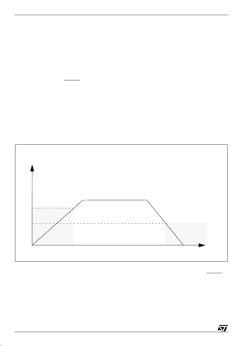
3.2.4 LVD Reset
The on-chip Low Voltage Detector, selectable as
user option, features static Reset when supply
voltage is below a reference value. Thanks to this
feature, external reset circuit can be removed
while keeping the application safety. This SAFE
RESET is effective as well in Power-on phase as
in power supply drop with different reference val
Figure 15. LVD Reset on Power-on and Power-down (Brown-out)
ues, allowing hysteresis effect. Reference value in
case of voltage drop has been set lower than the
reference value for power-on in order to avoid any
parasitic Reset when MCU start's running and
sinking current on the supply.
-
As long as the supply voltage is below the reference value, there is a internal and static RESET
command. The MCU can start only when the sup
ply voltage rises over the reference value. Therefore, only two operating mode exist for the MCU:
RESET active below the voltage reference, and
running mode over the voltage reference as
shown on the Figure 15, that represents a power-
up, power-down sequence.
Note: When the RESET state is controlled by one
of the internal RESET sources (Low Voltage De
tector, Watchdog, Power on Reset), the RESET
pin is tied to low logic level.
-
-
-
3.2.5 Application Notes
No external resistor is required between VDD and
the Reset pin, thanks to the built-in pull-up device.
23/83
Direct external connection of the pin RESET to
must be avoided in order to ensure safe be-
V
DD
haviour of the internal reset sources (AND.Wired
structure).

ST6253C ST6263C ST6263B ST6260C ST6260B
RESET
RESET
VECTOR
JP
JP:2 BYTES/4 CYCLES
RETI
RETI: 1 BYTE/2 CYCLES
INITIALIZATION
ROUTINE
VA00181
V
DD
RESET
R
PU
R
ESD
1)
POWER
WATCHDOG RESET
CK
COUNTER
RESET
ST6
INTERNAL
RESET
f
OSC
RESET
ON RESET
LVD RESET
VR02107A
AND. Wired
1) Resistive ESD protection. Value not guaranteed.
RESETS (Cont’d)
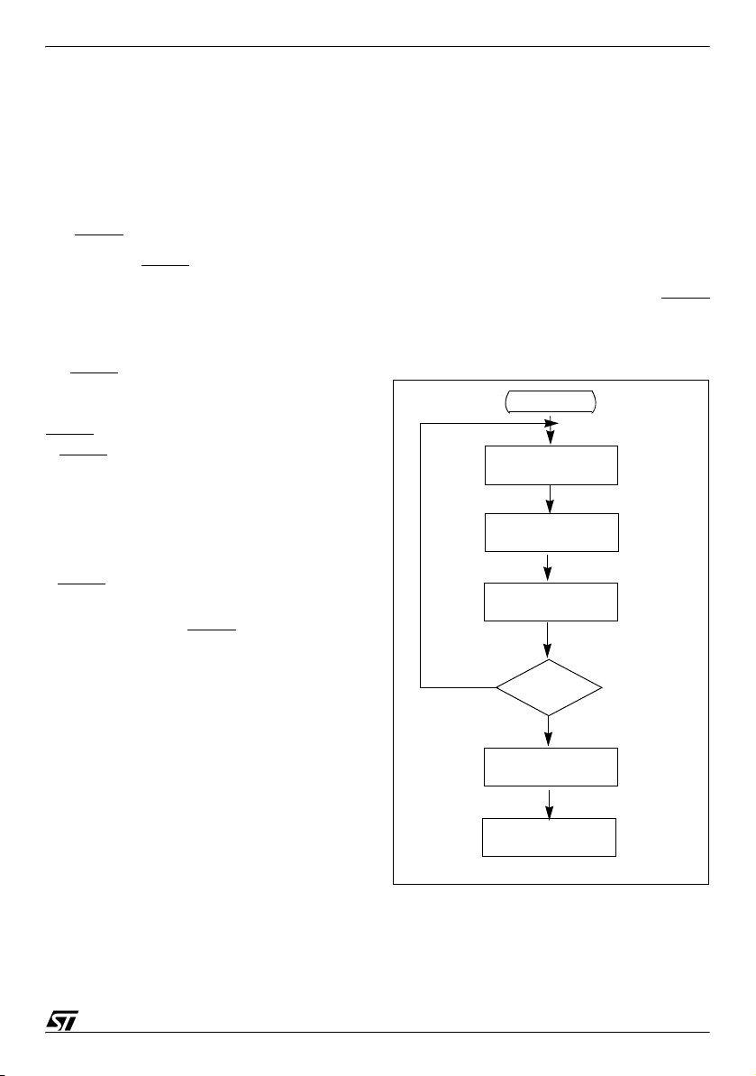
3.2.6 MCU Initialization Sequence
When a reset occurs the stack is reset, the PC is
loaded with the address of the Reset Vector (locat
ed in program ROM starting at address 0FFEh). A
jump to the beginning of the user program must be
coded at this address. Following a Reset, the In
terrupt flag is automatically set, so that the CPU is
in Non Maskable Interrupt mode; this prevents the
initialisation routine from being interrupted. The in
itialisation routine should therefore be terminated
by a RETI instruction, in order to revert to normal
mode and enable interrupts. If no pending interrupt
is present at the end of the initialisation routine, the
MCU will continue by processing the instruction
immediately following the RETI instruction. If, how
ever, a pending interrupt is present, it will be serviced.
Figure 17. Reset Block Diagram
Figure 16. Reset and Interrupt Processing
-
-
-
-
24/83

ST6253C ST6263C ST6263B ST6260C ST6260B
RESETS (Cont’d)
Table 5Register Reset Status
Register Address(es) Status Comment
Oscillator Control Register
EEPROM Control Register
Port Data Registers
Port Direction Register
Port Option Register
Interrupt Option Register
TIMER Status/Control
AR TIMER Mode Control Register
AR TIMER Status/Control 0 Register
AR TIMER Status/Control 1 Register
AR TIMER Compare Register
Miscellaneous Register
SPI Registers
SPI DIV Register
SPI MOD Register
SPI DSR Register
X, Y, V, W, Register
Accumulator
Data RAM
Data RAM Page REgister
Data ROM Window Register
EEPROM
A/D Result Register
AR TIMER Load Register
AR TIMER Reload/Capture Register
0DCh
0EAh
0C0h to 0C2h
0C4h to 0C6h
0CCh to 0CEh
0C8h
0D4h
0D5h
0D6h
0D7h
0DDh
0E0h to 0E2h
0E1h
0E2h
0E0h
080H TO 083H
0FFh
084h to 0BFh
0E8h
0C9h
00h to 03Fh
0D0h
0DBh
0D9h
00h
00h
00h
00h
00h
00h
00h
00h
00h
00h
00h
00h
00h
00h
00h
Undefined
Undefined
EEPROM disabled (if available)
I/O are Input with pull-up
I/O are Input with pull-up
I/O are Input with pull-up
Interrupt disabled
TIMER disabled
AR TIMER stopped
SPI Output not connected to PC3
SPI disabled
SPI disabled
SPI disabled
SPI disabled
As written if programmed
TIMER Counter Register
TIMER Prescaler Register
Watchdog Counter Register
A/D Control Register
25/83
0D3h
0D2h
0D8h
0D1h
FFh
7Fh
FEh
40h
Max count loaded
A/D in Standby
 Loading...