

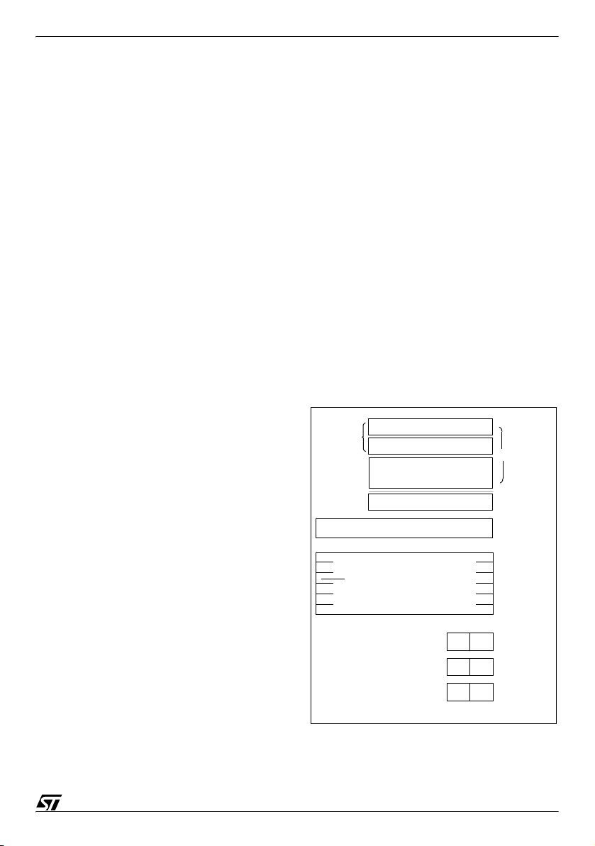
ST6253C ST6263C ST6263B
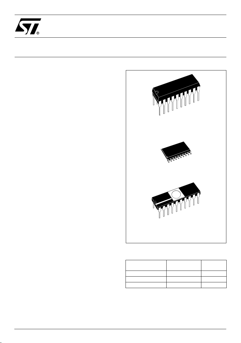
PDIP20
PSO20
CDIP20W
(See end of Datasheet for Ordering Information)
safe reset, auto-reload timer, EEPROM and SPI
Features
■ 3.0 to 6.0 V Supply Operating Range
■ 8 MHz Maximum Clock Frequency
■ -40 to +125°C Operating Temperature Range
■ Run, Wait and Stop Modes
■ 5 Interrupt Vectors
■ Look-up Table capability in Program Memory
■ Data Storage in Program Memory:
User selectable size
■ Data RAM: 128 bytes
■ Data EEPROM: 64/128 bytes (not in ST6253C
devices)
■ User Programmable Options
■ 13 I/O pins, fully programmable as:
– Input with pull-up resistor
– Input without pull-up resistor
– Input with interrupt generation
– Open-drain or push-pull output
– Analog Input
■ 6 I/O lines can sink up to 30 mA to drive LEDs or
TRIACs directly
■ 8-bit Timer / Counter with 7-bit programmable
prescaler
■ 8-bit Auto-reload Timer with 7-bit programmable
prescaler (AR Timer)
■ Digital Watchdog
■ Oscillator Safe Guard (not in ROM devices)
■ Low Voltage Detector for Safe Reset (not in
ROM devices)
■ 8-bit A/D Converter with 7 analog inputs
■ 8-bit Synchronous Peripheral Interface (SPI)
■ On-chip Clock oscillator can be driven by Quartz
Crystal Ceramic resonator or RC network
■ User configurable Power-on Reset
■ One external Non-Maskable Interrupt
■ ST626x-EMU2 Emulation and Development
System (connects to an MS-DOS PC via a
parallel port).
ST6260C ST6260B
8-bit MCUs with A/D converter,
DEVICE SUMMARY
DEVICE
ST6253C 1836 ST6260C / ST6260B 3884 128
ST6263C / ST6263B 1836 64
Program memory
(Bytes)
EEPROM
(Bytes)
March 2009 Rev. 3 1/83

Table of Contents
Document
Page
ST6253C ST6263C ST6263B
ST6260C ST6260B . . . . . . . . . . . . . . . . . . . . . . . . . . . . . . . . . . . . . 1
1 GENERAL DESCRIPTION . . . . . . . . . . . . . . . . . . . . . . . . . . . . . . . . . . . . . . . . . . . . . . . . . . . . . . 4
1.1 INTRODUCTION . . . . . . . . . . . . . . . . . . . . . . . . . . . . . . . . . . . . . . . . . . . . . . . . . . . . . . . . . 4
1.2 PIN DESCRIPTIONS . . . . . . . . . . . . . . . . . . . . . . . . . . . . . . . . . . . . . . . . . . . . . . . . . . . . . . 5
1.3 MEMORY MAP . . . . . . . . . . . . . . . . . . . . . . . . . . . . . . . . . . . . . . . . . . . . . . . . . . . . . . . . . . 6
1.4 PROGRAMMING MODES . . . . . . . . . . . . . . . . . . . . . . . . . . . . . . . . . . . . . . . . . . . . . . . . . 13
2 CENTRAL PROCESSING UNIT . . . . . . . . . . . . . . . . . . . . . . . . . . . . . . . . . . . . . . . . . . . . . . . . . 15
2.1 INTRODUCTION . . . . . . . . . . . . . . . . . . . . . . . . . . . . . . . . . . . . . . . . . . . . . . . . . . . . . . . . 15
2.2 CPU REGISTERS . . . . . . . . . . . . . . . . . . . . . . . . . . . . . . . . . . . . . . . . . . . . . . . . . . . . . . . 15
3 CLOCKS, RESET, INTERRUPTS AND POWER SAVING MODES . . . . . . . . . . . . . . . . . . . . . 17
3.1 CLOCK SYSTEM . . . . . . . . . . . . . . . . . . . . . . . . . . . . . . . . . . . . . . . . . . . . . . . . . . . . . . . . 17
3.2 RESETS . . . . . . . . . . . . . . . . . . . . . . . . . . . . . . . . . . . . . . . . . . . . . . . . . . . . . . . . . . . . . . . 22
3.3 DIGITAL WATCHDOG . . . . . . . . . . . . . . . . . . . . . . . . . . . . . . . . . . . . . . . . . . . . . . . . . . . . 26
3.4 INTERRUPTS . . . . . . . . . . . . . . . . . . . . . . . . . . . . . . . . . . . . . . . . . . . . . . . . . . . . . . . . . . 30
3.5 POWER SAVING MODES . . . . . . . . . . . . . . . . . . . . . . . . . . . . . . . . . . . . . . . . . . . . . . . . . 34
4 ON-CHIP PERIPHERALS . . . . . . . . . . . . . . . . . . . . . . . . . . . . . . . . . . . . . . . . . . . . . . . . . . . . . . 36
4.1 I/O PORTS . . . . . . . . . . . . . . . . . . . . . . . . . . . . . . . . . . . . . . . . . . . . . . . . . . . . . . . . . . . . . 36
4.2 TIMER . . . . . . . . . . . . . . . . . . . . . . . . . . . . . . . . . . . . . . . . . . . . . . . . . . . . . . . . . . . . . . . . 42
4.3 AUTO-RELOAD TIMER . . . . . . . . . . . . . . . . . . . . . . . . . . . . . . . . . . . . . . . . . . . . . . . . . . . 45
4.4 A/D CONVERTER (ADC) . . . . . . . . . . . . . . . . . . . . . . . . . . . . . . . . . . . . . . . . . . . . . . . . . 51
4.5 SERIAL PERIPHERAL INTERFACE (SPI) . . . . . . . . . . . . . . . . . . . . . . . . . . . . . . . . . . . . 53
4.6 SPI TIMING DIAGRAMS . . . . . . . . . . . . . . . . . . . . . . . . . . . . . . . . . . . . . . . . . . . . . . . . . . 56
5 SOFTWARE . . . . . . . . . . . . . . . . . . . . . . . . . . . . . . . . . . . . . . . . . . . . . . . . . . . . . . . . . . . . . . . . 58
5.1 ST6 ARCHITECTURE . . . . . . . . . . . . . . . . . . . . . . . . . . . . . . . . . . . . . . . . . . . . . . . . . . . . 58
5.2 ADDRESSING MODES . . . . . . . . . . . . . . . . . . . . . . . . . . . . . . . . . . . . . . . . . . . . . . . . . . . 58
5.3 INSTRUCTION SET . . . . . . . . . . . . . . . . . . . . . . . . . . . . . . . . . . . . . . . . . . . . . . . . . . . . . . 59
6 ELECTRICAL CHARACTERISTICS . . . . . . . . . . . . . . . . . . . . . . . . . . . . . . . . . . . . . . . . . . . . . . 64
6.1 ABSOLUTE MAXIMUM RATINGS . . . . . . . . . . . . . . . . . . . . . . . . . . . . . . . . . . . . . . . . . . . 64
6.2 RECOMMENDED OPERATING CONDITIONS . . . . . . . . . . . . . . . . . . . . . . . . . . . . . . . . . 65
6.3 DC ELECTRICAL CHARACTERISTICS . . . . . . . . . . . . . . . . . . . . . . . . . . . . . . . . . . . . . . 66
6.4 AC ELECTRICAL CHARACTERISTICS . . . . . . . . . . . . . . . . . . . . . . . . . . . . . . . . . . . . . . 67
6.5 A/D CONVERTER CHARACTERISTICS . . . . . . . . . . . . . . . . . . . . . . . . . . . . . . . . . . . . . . 68
6.6 TIMER CHARACTERISTICS . . . . . . . . . . . . . . . . . . . . . . . . . . . . . . . . . . . . . . . . . . . . . . . 68
6.7 SPI CHARACTERISTICS . . . . . . . . . . . . . . . . . . . . . . . . . . . . . . . . . . . . . . . . . . . . . . . . . 68
6.8 ARTIMER ELECTRICAL CHARACTERISTICS . . . . . . . . . . . . . . . . . . . . . . . . . . . . . . . . . 68
7 PACKAGE MECHANICAL DATA . . . . . . . . . . . . . . . . . . . . . . . . . . . . . . . . . . . . . . . . . . . . . . . . 74
8 ORDERING INFORMATION . . . . . . . . . . . . . . . . . . . . . . . . . . . . . . . . . . . . . . . . . . . . . . . . . . . . 76
8.1 OTP/EPROM VERSIONS . . . . . . . . . . . . . . . . . . . . . . . . . . . . . . . . . . . . . . . . . . . . . . . . . 76
8.2 FASTROM VERSIONS . . . . . . . . . . . . . . . . . . . . . . . . . . . . . . . . . . . . . . . . . . . . . . . . . . . 77
8.3 ROM VERSIONS . . . . . . . . . . . . . . . . . . . . . . . . . . . . . . . . . . . . . . . . . . . . . . . . . . . . . . . . 78
2/83

Table of Contents
9 REVISION HISTORY . . . . . . . . . . . . . . . . . . . . . . . . . . . . . . . . . . . . . . . . . . . . . . . . . . . . . . . . . . 82
Document
Page
3/83

ST6253C ST6263C ST6263B ST6260C ST6260B
TEST
NMI
INTERRUPT
PROGRAM
PC
STACK LEVEL 1
STACK LEVEL 2
STACK LEVEL 3
STACK LEVEL 4
STACK LEVEL 5
STACK LEVEL 6
POWER
SUPPLY
OSCILLATOR
RESET
DATA ROM
USER
SELECTABLE
DATA RAM
PORT A
PORT B
TIMER
DIGITAL
8 BIT CORE
TEST/V
PP
8-BIT
A/D CONVERTER
PA0..PA3 / Ain
PB0..PB3 / 30 mA Sink
VDDV
SS
OSCin OSCout RESET
WATCHDOG
MEMORY
PB6 / ARTimin / 30 mA Sink
PORT C
PC2 / Sin / Ain
PC3 / Sout / Ain
SPI (SERIAL
PERIPHERAL
INTERFACE)
AUTORELOAD
TIMER
PC4 / Sck / Ain
PB7 / ARTimout / 30 mA Sink
128 Bytes
1836 bytes OTP
3884 bytes OTP
3884 bytes EPROM
(ST62T53C,T63C)
(ST62T60C)
(ST62E60C)
DATA EEPROM
64 Bytes
128 Bytes
(ST62T60C/E60C)
(ST62T63C)
1 GENERAL DESCRIPTION
1.1 INTRODUCTION
The ST62T53C, ST62T60C, ST62T63C and
ST62E60C devices are low cost members of the
ST62xx 8-bit HCMOS family of microcontrollers,
which is targeted at low to medium complexity ap
plications. All ST62xx devices are based on a
building block approach: a common core is sur
rounded by a number of on-chip peripherals.
The ST62E60C is the erasable EPROM version of
the ST62T60C device, which may be used to em
ulate the ST62T53C, ST62T60C and ST62T63C
devices, as well as the respective ST6253C,
ST6260B and ST6263B ROM devices.
OTP and EPROM devices are functionally identical. The ROM based versions offer the same functionality selecting as ROM options the options de-
Figure 1. Block Diagram
-
-
-
fined in the programmable option byte of the OTP/
EPROM versions.
OTP devices offer all the advantages of user programmability at low cost, which make them the
ideal choice in a wide range of applications where
frequent code changes, multiple code versions or
last minute programmability are required.
These compact low-cost devices feature a Timer
comprising an 8-bit counter and a 7-bit program
mable prescaler, an 8-bit Auto-Reload Timer,
EEPROM data capability (except ST62T53C), a
serial port communication interface, an 8-bit A/D
Converter with 7 analog inputs and a Digital
Watchdog timer, making them well suited for a
wide range of automotive, appliance and industrial
applications.
4/83

ST6253C ST6263C ST6263B ST6260C ST6260B
1
2
3
4
5
6
7
8
9
10
11
12
13
14
15
16
17
18
19
20
PB0
PB1
V
PP
/TEST
PB2
PB3
Ain/PA0
V
SS
V
DD
PC2 / Sin / Ain
RESET
PA1/Ain
ARTIMin/PB6
ARTIMout/PB7
PC3 / Sout / Ain
PC4 / Sck / Ain
NMI
OSCin
OSCout
PA2/Ain
PA3/Ain
1.2 PIN DESCRIPTIONS
VDD and VSS. Power is supplied to the MCU via
these two pins. V
V
is the ground connection.
SS
OSCin and OSCout. These pins are internally
connected to the on-chip oscillator circuit. A quartz
crystal, a ceramic resonator or an external clock
signal can be connected between these two pins.
The OSCin pin is the input pin, the OSCout pin is
the output pin.
RESET. The active-low RESET pin is used to restart the microcontroller.
TEST/VPP. The TEST must be held at VSS for nor-
mal operation. If TEST pin is connected to a
+12.5V level during the reset phase, the EPROM/
OTP programming Mode is entered.
NMI. The NMI pin provides the capability for asynchronous interruption, by applying an external non
maskable interrupt to the MCU. It is provided with
an on-chip pullup resistor (if option has been ena
bled), and Schmitt trigger characteristics.
PA0-PA3. These 4 lines are organized as one I/O
port (A). Each line may be configured under soft
ware control as inputs with or without internal pullup resistors, interrupt generating inputs with pullup resistors, open-drain or push-pull outputs, ana
log inputs for the A/D converter.
PB0-PB3. These 4 lines are organized as one I/O
port (B). Each line may be configured under soft
ware control as inputs with or without internal pullup resistors, interrupt generating inputs with pullup resistors, open-drain or push-pull outputs.
PB0-PB3 can also sink 30mA for direct LED
driving.
is the power connection and
DD
-
-
-
-
PB6/ARTIMin, PB7/ARTIMout. These pins are either Port B I/O bits or the Input and Output pins of
the AR TIMER. To be used as timer input function
PB6 has to be programmed as input with or with
out pull-up. A dedicated bit in the AR TIMER Mode
Control Register sets PB7 as timer output function.
PB6-PB7 can also sink 30mA for direct LED driving.
PC2-PC4. These 3 lines are organized as one I/O
port (C). Each line may be configured under soft
ware control as input with or without internal pullup resistor, interrupt generating input with pull-up
resistor, analog input for the A/D converter, opendrain or push-pull output.
PC2-PC4 can also be used as respectively Data
in, Data out and Clock I/O pins for the on-chip SPI
to carry the synchronous serial I/O signals.
Figure 2ST62T53C/T60C/T63C/E60C Pin
Configuration
-
-
5/83
ST6253C ST6263C ST6263B ST6260C ST6260B
PROGRAM SPACE
PROGRAM
INTERRUPT &
RESET VECTORS
ACCUMULATOR
DATA RAM
BANK SELECT
WINDOW SELECT
RAM
X REGISTER
Y REGISTER
V REGISTER
W REGISTER
DATA READ-ONLY
WINDOW
RAM / EEPROM
BANKING AREA
000h
03Fh
040h
07Fh
080h
081h
082h
083h
084h
0C0h
0FFh
0-63
DATA SPACE
0000h
0FF0h
0FFFh
MEMORY
MEMORY
DATA READ-ONLY
MEMORY
1.3 MEMORY MAP
1.3.1 Introduction
The MCU operates in three separate memory
spaces: Program space, Data space, and Stack
space. Operation in these three memory spaces is
described in the following paragraphs.
Figure 3Memory Addressing Diagram
Briefly, Program space contains user program
code in OTP and user vectors; Data space con
tains user data in RAM and in OTP, and Stack
space accommodates six levels of stack for sub
routine and interrupt service routine nesting.
-
-
6/83

ST6253C ST6263C ST6263B ST6260C ST6260B
0000h
RESERVED
*
USER
PROGRAM MEMORY
(OTP/EPROM)
3872 BYTES
0F9Fh
0FA0h
0FEFh
0FF0h
0FF7h
0FF8h
0FFBh
0FFCh
0FFDh
0FFEh
0FFFh
RESERVED
*
RESERVED
INTERRUPT VECTORS
NMI VECTOR
USER RESET VECTOR
0080h
(*) Reserved areas should be filled with 0FFh
007Fh
0000h
RESERVED
*
USER
PROGRAM MEMORY
(OTP)
1824 BYTES
0F9Fh
0FA0h
0FEFh
0FF0h
0FF7h
0FF8h
0FFBh
0FFCh
0FFDh
0FFEh
0FFFh
RESERVED
*
RESERVED
INTERRUPT VECTORS
NMI VECTOR
USER RESET VECTOR
087Fh
(*) Reserved areas should be filled with 0FFh
0880h
MEMORY MAP (Cont’d)
1.3.2 Program Space
Program Space comprises the instructions to be
executed, the data required for immediate ad
dressing mode instructions, the reserved factory
test area and the user vectors. Program Space is
addressed via the 12-bit Program Counter register
(PC register).
1.3.2.1 Program Memory Protection
The Program Memory in OTP or EPROM devices
can be protected against external readout of mem
ory by selecting the READOUT PROTECTION option in the option byte.
Figure 4ST62E60C/T60C Program
Memory Map
In the EPROM parts, READOUT PROTECTION
-
option can be disactivated only by U.V. erasure
that also results into the whole EPROM context
erasure.
Note: Once the Readout Protection is activated, it
is no longer possible, even for STMicroelectronics,
to gain access to the OTP contents. Returned
parts with a protection set can therefore not be ac
cepted.
-
Figure 5ST62T53C/T63C Program
Memory Map
-
7/83
ST6253C ST6263C ST6263B ST6260C ST6260B
MEMORY MAP (Cont’d)
1.3.3 Data Space
Data Space accommodates all the data necessary
for processing the user program. This space com
prises the RAM resource, the processor core and
peripheral registers, as well as read-only data
such as constants and look-up tables in OTP/
EPROM.
1.3.3.1 Data ROM
All read-only data is physically stored in program
memory, which also accommodates the Program
Space. The program memory consequently con
tains the program code to be executed, as well as
the constants and look-up tables required by the
application.
The Data Space locations in which the different
constants and look-up tables are addressed by the
processor core may be thought of as a 64-byte
window through which it is possible to access the
read-only data stored in OTP/EPROM.
1.3.3.2 Data RAM/EEPROM
In ST62T53C, T60C, T63C and ST62E60C devices, the data space includes 60 bytes of RAM, the
accumulator (A), the indirect registers (X), (Y), the
short direct registers (V), (W), the I/O port regis
ters, the peripheral data and control registers, the
interrupt option register and the Data ROM Win
dow register (DRW register).
Additional RAM and EEPROM pages can also be
addressed using banks of 64 bytes located be
tween addresses 00h and 3Fh.
1.3.4 Stack Space
Stack space consists of six 12-bit registers which
are used to stack subroutine and interrupt return
addresses, as well as the current program counter
contents.
Table 1. Additional RAM/EEPROM Banks
Device RAM EEPROM
ST62T53C 1 x 64 bytes -
ST62T60C/E60C 1 x 64 bytes 2 x 64 bytes
ST62T63C 1 x 64 bytes 1 x 64 bytes
Table 2ST62T53C, T60C, T63C and ST62E60C
Data Memory Space
-
-
-
-
-
AR TIMER STATUS/CONTROL REGISTER1 0D6h
AR TIMER STATUS/CONTROL REGISTER2 0D7h
AR TIMER RELOAD/CAPTURE REGISTER 0D9h
* WRITE ONLY REGISTER
RAM and EEPROM
DATA ROM WINDOW AREA
X REGISTER 080h
Y REGISTER 081h
V REGISTER 082h
W REGISTER 083h
DATA RAM 60 BYTES
PORT A DATA REGISTER 0C0h
PORT B DATA REGISTER 0C1h
PORT C DATA REGISTER 0C2h
RESERVED 0C3h
PORT A DIRECTION REGISTER 0C4h
PORT B DIRECTION REGISTER 0C5h
PORT C DIRECTION REGISTER 0C6h
RESERVED 0C7h
INTERRUPT OPTION REGISTER 0C8h*
DATA ROM WINDOW REGISTER 0C9h*
RESERVED
PORT A OPTION REGISTER 0CCh
PORT B OPTION REGISTER 0CDh
PORT C OPTION REGISTER 0CEh
RESERVED 0CFh
A/D DATA REGISTER 0D0h
A/D CONTROL REGISTER 0D1h
TIMER PRESCALER REGISTER 0D2h
TIMER COUNTER REGISTER 0D3h
TIMER STATUS CONTROL REGISTER 0D4h
AR TIMER MODE CONTROL REGISTER 0D5h
WATCHDOG REGISTER 0D8h
AR TIMER COMPARE REGISTER 0DAh
AR TIMER LOAD REGISTER 0DBh
OSCILLATOR CONTROL REGISTER 0DCh*
MISCELLANEOUS 0DDh
RESERVED
SPI DATA REGISTER 0E0h
SPI DIVIDER REGISTER 0E1h
SPI MODE REGISTER 0E2h
RESERVED
DATA RAM/EEPROM REGISTER 0E8h*
RESERVED 0E9h
EEPROM CONTROL REGISTER
(except ST62T53C)
RESERVED
ACCUMULATOR 0FFh
000h
03Fh
040h
07Fh
084h
0BFh
0CAh
0CBh
0DEh
0DFh
0E3h
0E7h
0EAh
0EBh
0FEh
8/83
ST6253C ST6263C ST6263B ST6260C ST6260B
DATA ROM
WINDOW REGISTER
CONTENTS
DATA SPACE ADDRESS
40h-7Fh
IN INSTRUCTION
PROGRAM SPACE ADDRESS
765432 0
543210
543210
READ
1
67891011
0
1
VR01573C
12
1
0
DATA SPACE ADDRESS
:
:
59h
000
0
1
00
1
11
Example:
(DWR)
DWR=28h
11
0000000
1
ROM
ADDRESS:A19h
11
13
0
1
MEMORY MAP (Cont’d)
1.3.5 Data Window Register (DWR)
The Data read-only memory window is located from
address 0040h to address 007Fh in Data space. It
allows direct reading of 64 consecutive bytes locat
ed anywhere in program memory, between address 0000h and 0FFFh (top memory address depends on the specific device). All the program
memory can therefore be used to store either in
structions or read-only data. Indeed, the window
can be moved in steps of 64 bytes along the pro
gram memory by writing the appropriate code in the
Data Window Register (DWR).
The DWR can be addressed like any RAM location
in the Data Space, it is however a write-only regis
ter and therefore cannot be accessed using singlebit operations. This register is used to position the
64-byte read-only data window (from address 40h
to address 7Fh of the Data space) in program
memory in 64-byte steps. The effective address of
the byte to be read as data in program memory is
obtained by concatenating the 6 least significant
bits of the register address given in the instruction
(as least significant bits) and the content of the
DWR register (as most significant bits), as illustrat
ed in Figure 6 below. For instance, when addressing location 0040h of the Data Space, with 0 loaded in the DWR register, the physical location addressed in program memory is 00h. The DWR register is not cleared on reset, therefore it must be
written to prior to the first access to the Data readonly memory window area.
Figure 6Data read-only memory Window Memory Addressing
Data Window Register (DWR)
Address: 0C9h — Write Only
7 0
-
- - DWR5 DWR4 DWR3 DWR2 DWR1 DWR0
Bits 6, 7 = Not used.
Bit 5-0 = DWR6-DWR0: Data read-only memory
Window Register Bits. These are the Data read-
only memory Window bits that correspond to the
upper bits of the data read-only memory space.
Caution: This register is undefined on reset. Nei-
-
ther read nor single bit instructions may be used to
address this register.
Note: Care is required when handling the DWR
register as it is write only. For this reason, the
DWR contents should not be changed while exe
cuting an interrupt service routine, as the service
routine cannot save and then restore the register’s
previous contents. If it is impossible to avoid writ
ing to the DWR during the interrupt service routine,
-
an image of the register must be saved in a RAM
location, and each time the program writes to the
DWR, it must also write to the image register. The
image register must be written first so that, if an in
terrupt occurs between the two instructions, the
DWR is not affected.
-
-
-
9/83

ST6253C ST6263C ST6263B ST6260C ST6260B
MEMORY MAP (Cont’d)
1.3.6 Data RAM/EEPROM Bank Register (DRBR)
Address: E8h — Write only
7 0
- - -
DRBR
4
- -
DRBR1DRBR
Bit 7-5 = These bits are not used
Bit 4 - DRBR4. This bit, when set, selects RAM
Page 2.
Bit 3-2 - Reserved. These bits are not used.
Bit 1 - DRBR1. This bit, when set, selects
EEPROM Page 1, when available.
Bit 0 - DRBR0. This bit, when set, selects
EEPROM Page 0, when available.
The selection of the bank is made by programming
the Data RAM Bank Switch register (DRBR regis
ter) located at address E8h of the Data Space according to Table 1. No more than one bank should
be set at a time.
The DRBR register can be addressed like a RAM
Data Space at the address E8h; nevertheless it is
a write only register that cannot be accessed with
single-bit operations. This register is used to select
the desired 64-byte RAM/EEPROM bank of the
Data Space. The bank number has to be loaded in
the DRBR register and the instruction has to point
Table 3Data RAM Bank Register Set-up
DRBR ST62T53C ST62T60C/E60C ST62T63C
to the selected location as if it was in bank 0 (from
00h address to 3Fh address).
This register is not cleared during the MCU initialization, therefore it must be written before the first
access to the Data Space bank region. Refer to
the Data Space description for additional informa
0
tion. The DRBR register is not modified when an
interrupt or a subroutine occurs.
Notes :
Care is required when handling the DRBR register
as it is write only. For this reason, it is not allowed
to change the DRBR contents while executing in
terrupt service routine, as the service routine cannot save and then restore its previous content. If it
is impossible to avoid the writing of this register in
interrupt service routine, an image of this register
must be saved in a RAM location, and each time
the program writes to DRBR it must write also to
the image register. The image register must be
-
written first, so if an interrupt occurs between the
two instructions the DRBR is not affected.
In DRBR Register, only 1 bit must be set. Otherwise two or more pages are enabled in parallel,
producing errors.
Care must also be taken not to change the
E²PROM page (when available) when the parallel
writing mode is set for the E²PROM, as defined in
EECTL register.
-
-
00 None None None
01 Not Available EEPROM Page 0 EEPROM Page 0
02 Not Available EEPROM Page 1 Not Available
08 Not Available Not Available Not Available
10h RAM Page 2 RAM Page 2 RAM Page 2
other Reserved Reserved Reserved
10/83

ST6253C ST6263C ST6263B ST6260C ST6260B
MEMORY MAP (Cont’d)
1.3.7 EEPROM Description
EEPROM memory is located in 64-byte pages in
data space. This memory may be used by the user
program for non-volatile data storage.
Data space from 00h to 3Fh is paged as described
in Table 4. EEPROM locations are accessed di
rectly by addressing these paged sections of data
space.
The EEPROM does not require dedicated instructions for read or write access. Once selected via the
Data RAM Bank Register, the active EEPROM
page is controlled by the EEPROM Control Regis
ter (EECTL), which is described below.
Bit E20FF of the EECTL register must be reset prior
to any write or read access to the EEPROM. If no
bank has been selected, or if E2OFF is set, any ac
cess is meaningless.
Programming must be enabled by setting the
E2ENA bit of the EECTL register.
The E2BUSY bit of the EECTL register is set when
the EEPROM is performing a programming cycle.
Any access to the EEPROM when E2BUSY is set
is meaningless.
Provided E2OFF and E2BUSY are reset, an EEPROM location is read just like any other data location, also in terms of access time.
Writing to the EEPROM may be carried out in two
modes: Byte Mode (BMODE) and Parallel Mode
Table 4. Row Arrangement for Parallel Writing of EEPROM Locations
Byte 0 1 2 3 4 5 6 7
ROW7 38h-3Fh
ROW6 30h-37h
ROW5 28h-2Fh
ROW4 20h-27h
ROW3 18h-1Fh
ROW2 10h-17h
ROW1 08h-0Fh
ROW0 00h-07h
(PMODE). In BMODE, one byte is accessed at a
time, while in PMODE up to 8 bytes in the same
row are programmed simultaneously (with conse
quent speed and power consumption advantages,
the latter being particularly important in battery
powered circuits).
General Notes:
Data should be written directly to the intended address in EEPROM space. There is no buffer memory between data RAM and the EEPROM space.
When the EEPROM is busy (E2BUSY = “1”)
-
EECTL cannot be accessed in write mode, it is
only possible to read the status of E2BUSY. This
implies that as long as the EEPROM is busy, it is
not possible to change the status of the EEPROM
Control Register. EECTL bits 4 and 5 are reserved
and must never be set.
Care is required when dealing with the EECTL register, as some bits are write only. For this reason,
the EECTL contents must not be altered while ex
ecuting an interrupt service routine.
If it is impossible to avoid writing to this register
within an interrupt service routine, an image of the
register must be saved in a RAM location, and
each time the program writes to EECTL it must
also write to the image register. The image register
must be written to first so that, if an interrupt oc
curs between the two instructions, the EECTL will
not be affected.
Dataspace
addresses.
Banks 0 and 1.
-
-
-
Up to 8 bytes in each row may be programmed simultaneously in Parallel Write mode.
The number of available 64-byte banks (1 or 2) is device dependent.
Note: The EEPROM is disabled as soon as STOP instruction is executed in order to achieve the lowest
power-consumption.
11/83

ST6253C ST6263C ST6263B ST6260C ST6260B
MEMORY MAP (Cont’d)
Additional Notes on Parallel Mode:
If the user wishes to perform parallel programming, the first step should be to set the E2PAR2
bit. From this time on, the EEPROM will be ad
dressed in write mode, the ROW address and the
data will be latched and it will be possible to
change them only at the end of the programming
cycle or by resetting E2PAR2 without program
ming the EEPROM. After the ROW address is
latched, the MCU can only “see” the selected
EEPROM row and any attempt to write or read
other rows will produce errors.
The EEPROM should not be read while E2PAR2
is set.
As soon as the E2PAR2 bit is set, the 8 volatile
ROW latches are cleared. From this moment on,
the user can load data in all or in part of the ROW.
Setting E2PAR1 will modify the EEPROM regis
ters corresponding to the ROW latches accessed
after E2PAR2. For example, if the software sets
E2PAR2 and accesses the EEPROM by writing to
addresses 18h, 1Ah and 1Bh, and then sets
E2PAR1, these three registers will be modified si
multaneously; the remaining bytes in the row will
be unaffected.
Note that E2PAR2 is internally reset at the end of
the programming cycle. This implies that the user
must set the E2PAR2 bit between two parallel pro
gramming cycles. Note that if the user tries to set
E2PAR1 while E2PAR2 is not set, there will be no
programming cycle and the E2PAR1 bit will be un
affected. Consequently, the E2PAR1 bit cannot be
set if E2ENA is low. The E2PAR1 bit can be set by
the user, only if the E2ENA and E2PAR2 bits are
also set.
Notes: The EEPROM page shall not be changed
through the DRBR register when the E2PAR2 bit
is set.
EEPROM Control Register (EECTL)
Address: EAh — Read/Write
Reset status: 00h
-
7 0
E2O
D7
-
FF
D5 D4
E2PAR1E2PAR2E2BUSYE2E
Bit 7 = D7: Unused.
Bit 6 = E2OFF: Stand-by Enable Bit. WRITE ONLY.
If this bit is set the EEPROM is disabled (any access
will be meaningless) and the power consumption of
the EEPROM is reduced to its lowest value.
Bit 5-4 = D5-D4: Reserved. MUST be kept reset.
Bit 3 = E2PAR1: Parallel Start Bit. WRITE ONLY.
Once in Parallel Mode, as soon as the user software
-
sets the E2PAR1 bit, parallel writing of the 8 adja
cent registers will start. This bit is internally reset at
the end of the programming procedure. Note that
less than 8 bytes can be written if required, the un
defined bytes being unaffected by the parallel pro-
-
gramming cycle; this is explained in greater detail in
the Additional Notes on Parallel Mode overleaf.
Bit 2 = E2PAR2: Parallel Mode En. Bit. WRITE
ONLY. This bit must be set by the user program in
order to perform parallel programming. If E2PAR2
-
is set and the parallel start bit (E2PAR1) is reset,
up to 8 adjacent bytes can be written simultane
ously. These 8 adjacent bytes are considered as a
-
row, whose address lines A7, A6, A5, A4, A3 are
fixed while A2, A1 and A0 are the changing bits, as
illustrated in
Table 4. E2PAR2 is automatically re-
set at the end of any parallel programming procedure. It can be reset by the user software before
starting the programming procedure, thus leaving
the EEPROM registers unchanged.
Bit 1 = E2BUSY: EEPROM Busy Bit. READ ON-
LY. This bit is automatically set by the EEPROM
control logic when the EEPROM is in program
ming mode. The user program should test it before
any EEPROM read or write operation; any attempt
to access the EEPROM while the busy bit is set
will be aborted and the writing procedure in
progress will be completed.
Bit 0 = E2ENA: EEPROM Enable Bit. WRITE ON-
LY. This bit enables programming of the EEPROM
cells. It must be set before any write to the EEP
ROM register. Any attempt to write to the EEPROM when E2ENA is low is meaningless and will
not trigger a write cycle.
The EEPROM is disabled as soon as a STOP instruction is executed in order to achieve the lowest
power-consumption.
NA
-
-
-
-
-
12/83

ST6253C ST6263C ST6263B ST6260C ST6260B
1.4 PROGRAMMING MODES
1.4.1 Option Bytes
The two Option Bytes allow configuration capability to the MCUs. Option byte’s content is automatically read, and the selected options enabled, when
the chip reset is activated.
It can only be accessed during the programming
mode. This access is made either automatically
(copy from a master device) or by selecting the
OPTION BYTE PROGRAMMING mode of the pro
grammer.
The option bytes are located in a non-user map.
No address has to be specified.
EPROM Code Option Byte (LSB)
7 0
PRO-
EXTC-
PB2-3
TECT
NTL
PULL
PB0-1
PULL
WDACT
DELAY
OSCIL OSGEN
EPROM Code Option Byte (MSB)
15 8
- - -
ADC
SYNCHRO
- -
NMI
PULL
D15-D13. Reserved. Must be cleared.
ADC SYNCHRO. When set, an A/D conversion is
started upon WAIT instruction execution, in order
to reduce supply noise. When this bit is low, an A/
D conversion is started as soon as the STA bit of
the A/D Converter Control Register is set.
D11. Reserved, must be set to one.
D10. Reserved, must be cleared.
NMI PULL. NMI Pull-Up. This bit must be set high
to configure the NMI pin with a pull-up resistor.
When it is low, no pull-up is provided.
LVD. LVD RESET enable.When this bit is set, safe
RESET is performed by MCU when the supply
-
LVD
voltage is too low. When this bit is cleared, only
power-on reset or external RESET are active.
PROTECT. Readout Protection. This bit allows the
protection of the software contents against piracy.
When the bit PROTECT is set high, readout of the
OTP contents is prevented by hardware.. When
this bit is low, the user program can be read.
EXTCNTL. External STOP MODE control.. When
EXTCNTL is high, STOP mode is available with
watchdog active by setting NMI pin to one. When
EXTCNTL is low, STOP mode is not available with
the watchdog active.
PB2-3 PULL. When set this bit removes pull-up at
reset on PB2-PB3 pins. When cleared PB2-PB3
pins have an internal pull-up resistor at reset.
PB0-1 PULL. When set this bit removes pull-up at
reset on PB0-PB1 pins. When cleared PB0-PB1
pins have an internal pull-up resistor at reset.
WDACT. This bit controls the watchdog activation.
When it is high, hardware activation is selected.
The software activation is selected when WDACT
is low.
DELAY. This bit enables the selection of the delay
internally generated after the internal reset (exter
nal pin, LVD, or watchdog activated) is released.
When DELAY is low, the delay is 2048 cycles of
the oscillator, it is of 32768 cycles when DELAY is
high.
OSCIL. Oscillator selection. When this bit is low,
the oscillator must be controlled by a quartz crys
tal, a ceramic resonator or an external frequency.
When it is high, the oscillator must be controlled by
an RC network, with only the resistor having to be
externally provided.
OSGEN. Oscillator Safe Guard. This bit must be
set high to enable the Oscillator Safe Guard.
When this bit is low, the OSG is disabled.
The Option byte is written during programming either by using the PC menu (PC driven Mode) or
automatically (stand-alone mode).
-
-
13/83

ST6253C ST6263C ST6263B ST6260C ST6260B
PROGRAMMING MODES (Cont’d)
1.4.2 EPROM Erasing
The EPROM of the windowed package of the
MCUs may be erased by exposure to Ultra Violet
light. The erasure characteristic of the MCUs is
such that erasure begins when the memory is ex
posed to light with a wave lengths shorter than approximately 4000Å. It should be noted that sunlights and some types of fluorescent lamps have
wavelengths in the range 3000-4000Å.
It is thus recommended that the window of the
MCUs packages be covered by an opaque label to
prevent unintentional erasure problems when test
ing the application in such an environment.
The recommended erasure procedure of the
MCUs EPROM is the exposure to short wave ul
-
traviolet light which have a wave-length 2537A.
The integrated dose (i.e. U.V. intensity x exposure
time) for erasure should be a minimum of 15W-
2
. The erasure time with this dosage is ap-
sec/cm
proximately 15 to 20 minutes using an ultraviolet
lamp with 12000µW/cm
2
power rating. The
ST62E60C should be placed within 2.5cm (1Inch)
of the lamp tubes during erasure.
-
-
14/83

ST6253C ST6263C ST6263B ST6260C ST6260B
PROGRAM
RESET
OPCODE
FLAG
VALUES
2
CONTROLLER
FLAGS
ALU
A-DATA
B-DATA
ADDRESS/READ LINE
DATA SPACE
INTERRUPTS
DATA
RAM/EEPROM
DATA
ROM/EPROM
RESULTS TO DATA SPACE (WRITE LINE)
ROM/EPROM
DEDICATIONS
ACCUMULATOR
CONTROL
SIGNALS
OSCin
OSCout
ADDRESS
DECODER
256
12
Program Counter
and
6 LAYER STACK
0,01 TO 8MHz
VR01811
2 CENTRAL PROCESSING UNIT
2.1 INTRODUCTION
The CPU Core of ST6 devices is independent of the
I/O or Memory configuration. As such, it may be
thought of as an independent central processor
communicating with on-chip I/O, Memory and Pe
ripherals via internal address, data, and control
buses. In-core communication is arranged as
shown in Figure 7; the controller being externally
linked to both the Reset and Oscillator circuits,
while the core is linked to the dedicated on-chip pe
ripherals via the serial data bus and indirectly, for
interrupt purposes, through the control registers.
2.2 CPU REGISTERS
The ST6 Family CPU core features six registers and
three pairs of flags available to the programmer.
These are described in the following paragraphs.
Accumulator (A). The accumulator is an 8-bit
general purpose register used in all arithmetic cal
culations, logical operations, and data manipulations. The accumulator can be addressed in Data
space as a RAM location at address FFh. Thus the
ST6 can manipulate the accumulator just like any
other register in Data space.
Figure 7. ST6 Core Block Diagram
-
-
-
Indirect Registers (X, Y). These two indirect registers are used as pointers to memory locations in
Data space. They are used in the register-indirect
addressing mode. These registers can be ad
dressed in the data space as RAM locations at addresses 80h (X) and 81h (Y). They can also be accessed with the direct, short direct, or bit direct addressing modes. Accordingly, the ST6 instruction
set can use the indirect registers as any other reg
ister of the data space.
Short Direct Registers (V, W). These two registers are used to save a byte in short direct addressing mode. They can be addressed in Data
space as RAM locations at addresses 82h (V) and
83h (W). They can also be accessed using the di
rect and bit direct addressing modes. Thus, the
ST6 instruction set can use the short direct regis
ters as any other register of the data space.
Program Counter (PC). The program counter is a
12-bit register which contains the address of the
next ROM location to be processed by the core.
This ROM location may be an opcode, an oper
and, or the address of an operand. The 12-bit
length allows the direct addressing of 4096 bytes
in Program space.
-
-
-
-
-
15/83
CPU REGISTERS (Cont’d)
SHORT
DIRECT
ADDRESSING
MODE
VREGISTER
WREGISTER
PROGRAM COUNTER
SIX LEVELS
STACK REGISTER
CZNORMAL FLAGS
INTERRUPT FLAGS
NMI FLAGS
INDEX
REGISTER
VA000423
b7
b7
b7
b7
b7
b0
b0
b0
b0
b0
b0b11
ACCUMULATOR
Y REG. POINTER
X REG. POINTER
CZ
CZ
However, if the program space contains more than
4096 bytes, the additional memory in program
space can be addressed by using the Program
Bank Switch register.
The PC value is incremented after reading the address of the current instruction. To execute relative
jumps, the PC and the offset are shifted through
the ALU, where they are added; the result is then
shifted back into the PC. The program counter can
be changed in the following ways:
- JP (Jump) instructionPC=Jump address
- CALL instructionPC= Call address
- Relative Branch Instruction.PC= PC +/- offset
- Interrupt PC=Interrupt vector
- Reset PC= Reset vector
- RET & RETI instructionsPC= Pop (stack)
- Normal instructionPC= PC + 1
Flags (C, Z). The ST6 CPU includes three pairs of
flags (Carry and Zero), each pair being associated
with one of the three normal modes of operation:
Normal mode, Interrupt mode and Non Maskable
Interrupt mode. Each pair consists of a CARRY
flag and a ZERO flag. One pair (CN, ZN) is used
during Normal operation, another pair is used dur
ing Interrupt mode (CI, ZI), and a third pair is used
in the Non Maskable Interrupt mode (CNMI, ZN
MI).
The ST6 CPU uses the pair of flags associated
with the current mode: as soon as an interrupt (or
a Non Maskable Interrupt) is generated, the ST6
CPU uses the Interrupt flags (resp. the NMI flags)
instead of the Normal flags. When the RETI in
struction is executed, the previously used set of
flags is restored. It should be noted that each flag
set can only be addressed in its own context (Non
Maskable Interrupt, Normal Interrupt or Main rou
tine). The flags are not cleared during context
switching and thus retain their status.
The Carry flag is set when a carry or a borrow occurs during arithmetic operations; otherwise it is
cleared. The Carry flag is also set to the value of
the bit tested in a bit test instruction; it also partici
pates in the rotate left instruction.
The Zero flag is set if the result of the last arithmetic or logical operation was equal to zero; otherwise it is cleared.
Switching between the three sets of flags is performed automatically when an NMI, an interrupt or
a RETI instructions occurs. As the NMI mode is
ST6253C ST6263C ST6263B ST6260C ST6260B
automatically selected after the reset of the MCU,
the ST6 core uses at first the NMI flags.
Stack. The ST6 CPU includes a true LIFO hardware stack which eliminates the need for a stack
pointer. The stack consists of six separate 12-bit
RAM locations that do not belong to the data
space RAM area. When a subroutine call (or inter
rupt request) occurs, the contents of each level are
shifted into the next higher level, while the content
of the PC is shifted into the first level (the original
contents of the sixth stack level are lost). When a
subroutine or interrupt return occurs (RET or RETI
instructions), the first level register is shifted back
into the PC and the value of each level is popped
back into the previous level. Since the accumula
tor, in common with all other data space registers,
is not stored in this stack, management of these
registers should be performed within the subrou
tine. The stack will remain in its “deepest” position
if more than 6 nested calls or interrupts are execut
ed, and consequently the last return address will
be lost. It will also remain in its highest position if
the stack is empty and a RET or RETI is executed.
In this case the next instruction will be executed.
Figure 8. ST6 CPU Programming Mode
l
-
-
-
-
-
-
-
-
-
16/83
ST6253C ST6263C ST6263B ST6260C ST6260B
INTEGRATED CLOCK
CRYSTAL/RESONATOR option
OSG ENABLED option
OSC
in
OSC
out
C
L1n
C
L2
ST6xxx
CRYSTAL/RESONATOR CLOCK
CRYSTAL/RESONATOR option
OSC
in
OSC
out
ST6xxx
EXTERNAL CLOCK
CRYSTAL/RESONATOR option
NC
OSC
in
OSC
out
ST6xxx
NC
OSC
in
OSC
out
R
NET
ST6xxx
RC NETWORK
RC NETWORK option
NC
3 CLOCKS, RESET, INTERRUPTS AND POWER SAVING MODES
3.1 CLOCK SYSTEM
The MCU features a Main Oscillator which can be
driven by an external clock, or used in conjunction
with an AT-cut parallel resonant crystal or a suita
ble ceramic resonator, or with an external resistor
). In addition, a Low Frequency Auxiliary Os-
(R
NET
cillator (LFAO) can be switched in for security reasons, to reduce power consumption, or to offer the
benefits of a back-up clock system.
The Oscillator Safeguard (OSG) option filters
spikes from the oscillator lines, provides access to
the LFAO to provide a backup oscillator in the
event of main oscillator failure and also automati
cally limits the internal clock frequency (f
function of V
ation. These functions are illustrated in Figure 10,
Figure 11, Figure 12 and Figure 13.
A programmable divider on F
order to adjust the internal clock of the MCU to the
, in order to guarantee correct oper-
DD
is also provided in
INT
INT
) as a
best power consumption and performance tradeoff.
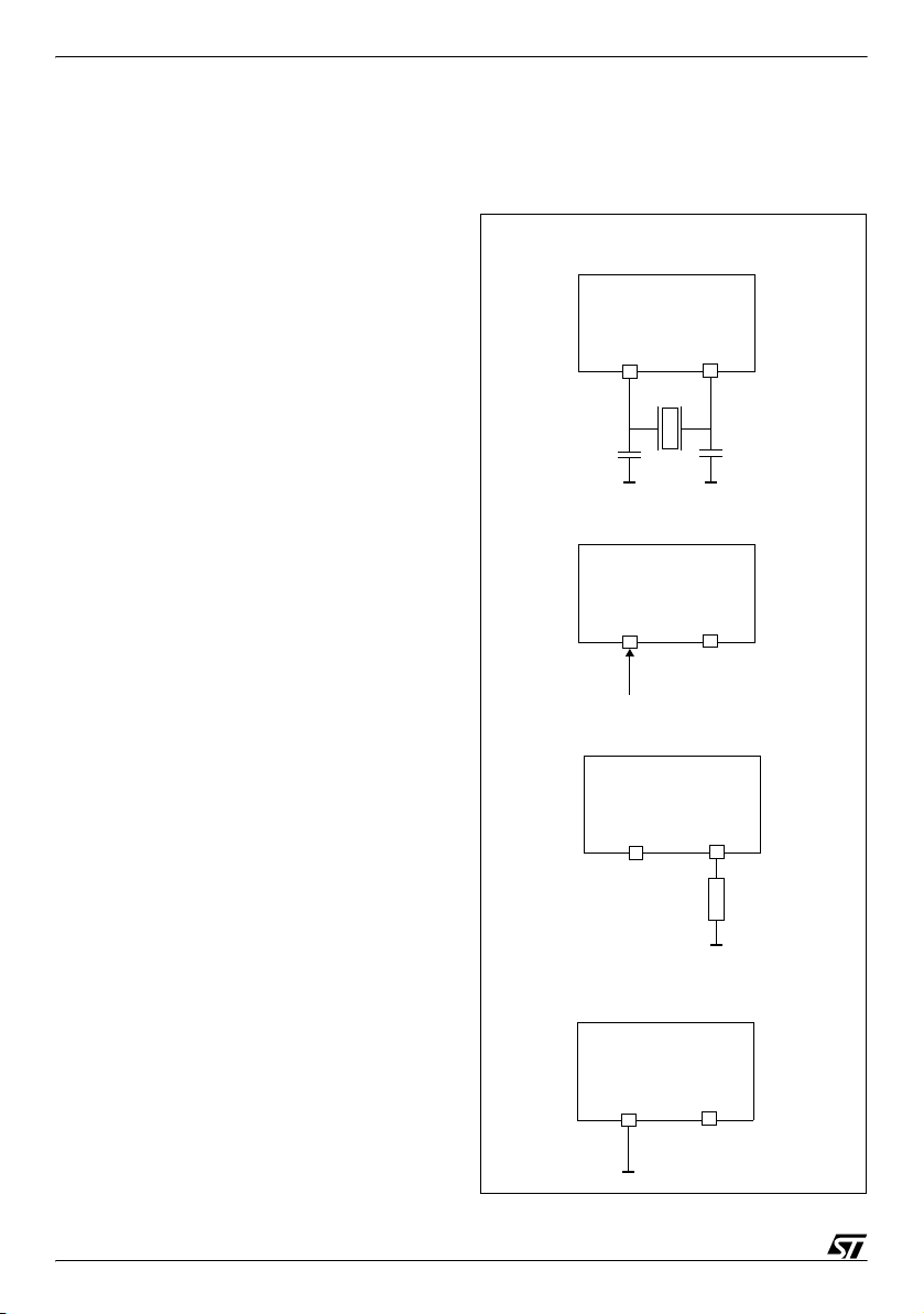
Figure 9 illustrates various possible oscillator con-
figurations using an external crystal or ceramic resonator, an external clock input, an external resistor
(R
LFAO. C
range 12 to 22 pF for an oscillator frequency in the
4-8 MHz range.
The internal MCU clock frequency (f
by 12 to drive the Timer, the A/D converter and the
Watchdog timer, and by 13 to drive the CPU core,
as may be seen in Figure 12.
), or the lowest cost solution using only the
NET
an CL2 should have a capacitance in the
L1
) is divided
INT
With an 8 MHz oscillator frequency, the fastest machine cycle is therefore 1.625µs.
A machine cycle is the smallest unit of time needed
to execute any operation (for instance, to increment
the Program Counter). An instruction may require
two, four, or five machine cycles for execution.
3.1.1 Main Oscillator
The oscillator configuration may be specified by selecting the appropriate option. When the CRYSTAL/
RESONATOR option is selected, it must be used with
a quartz crystal, a ceramic resonator or an external
signal provided on the OSCin pin. When the RC NET
WORK option is selected, the system clock is generated by an external resistor.
The main oscillator can be turned off (when the
OSG ENABLED option is selected) by setting the
OSCOFF bit of the ADC Control Register. The
Low Frequency Auxiliary Oscillator is automatical
ly started.
Figure 9. Oscillator Configurations
-
-
-
-
17/83

ST6253C ST6263C ST6263B ST6260C ST6260B
CLOCK SYSTEM (Cont’d)
Turning on the main oscillator is achieved by resetting the OSCOFF bit of the A/D Converter Control Register or by resetting the MCU. Restarting
the main oscillator implies a delay comprising the
oscillator start up delay period plus the duration of
the software instruction at f
3.1.2 Low Frequency Auxiliary Oscillator (LFAO)
The Low Frequency Auxiliary Oscillator has three
main purposes. Firstly, it can be used to reduce
power consumption in non timing critical routines.
Secondly, it offers a fully integrated system clock,
without any external components. Lastly, it acts as
a safety oscillator in case of main oscillator failure.
This oscillator is available when the OSG ENABLED option is selected. In this case, it automatically starts one of its periods after the first missing
edge from the main oscillator, whatever the reason
(main oscillator defective, no clock circuitry provid
ed, main oscillator switched off...).
User code, normal interrupts, WAIT and STOP instructions, are processed as normal, at the reduced f
cy is decreased, since the internal frequency is be-
frequency. The A/D converter accura-
LFAO
low 1MHz.
At power on, the Low Frequency Auxiliary Oscilla-
tor starts faster than the Main Oscillator. It therefore feeds the on-chip counter generating the POR
delay until the Main Oscillator runs.
The Low Frequency Auxiliary Oscillator is automatically switched off as soon as the main oscillator starts.
ADCR
Address: 0D1h — Read/Write
7 0
ADCR7ADCR6ADCR5ADCR4ADCR3OSC
Bit 7-3, 1-0= ADCR7-ADCR3, ADCR1-ADCR0:
ADC Control Register. These bits are reserved for
ADC Control.
Bit 2 = OSCOFF. When low, this bit enables main
oscillator to run. The main oscillator is switched off
when OSCOFF is high.
3.1.3 Oscillator Safe Guard
The Oscillator Safe Guard (OSG) affords drastically increased operational integrity in ST62xx devices. The OSG circuit provides three basic func-
clock frequency.
LFAO
OFF
ADCR1ADCR
0
-
tions: it filters spikes from the oscillator lines which
would result in over frequency to the ST62 CPU; it
gives access to the Low Frequency Auxiliary Os
cillator (LFAO), used to ensure minimum processing in case of main oscillator failure, to offer reduced power consumption or to provide a fixed frequency low cost oscillator; finally, it automatically
limits the internal clock frequency as a function of
supply voltage, in order to ensure correct opera
tion even if the power supply should drop.
The OSG is enabled or disabled by choosing the
relevant OSG option. It may be viewed as a filter
whose cross-over frequency is device dependent.
Spikes on the oscillator lines result in an effectively
increased internal clock frequency. In the absence
of an OSG circuit, this may lead to an over fre
quency for a given power supply voltage. The
OSG filters out such spikes (as illustrated in Figure
10). In all cases, when the OSG is active, the max
imum internal clock frequency, f
, which is supply voltage dependent. This re-
f
OSG
lationship is illustrated in Figure 13.
, is limited to
INT
When the OSG is enabled, the Low Frequency
Auxiliary Oscillator may be accessed. This oscilla
tor starts operating after the first missing edge of
the main oscillator (see Figure 11).
Over-frequency, at a given power supply level, is
seen by the OSG as spikes; it therefore filters out
some cycles in order that the internal clock fre
quency of the device is kept within the range the
particular device can stand (depending on V
and below f
cy with OSG enabled.
: the maximum authorised frequen-
OSG
DD
),
Note. The OSG should be used wherever possible
as it provides maximum safety. Care must be tak
en, however, as it can increase power consumption and reduce the maximum operating frequency
.
to f
OSG
Warning: Care has to be taken when using the
OSG, as the internal frequency is defined between
a minimum and a maximum value and is not accu
rate.
For precise timing measurements, it is not recommended to use the OSG and it should not be enabled in applications that use the SPI or the UART.
It should also be noted that power consumption in
Stop mode is higher when the OSG is enabled
(around 50µA at nominal conditions and room
temperature).
-
-
-
-
-
-
-
-
18/83
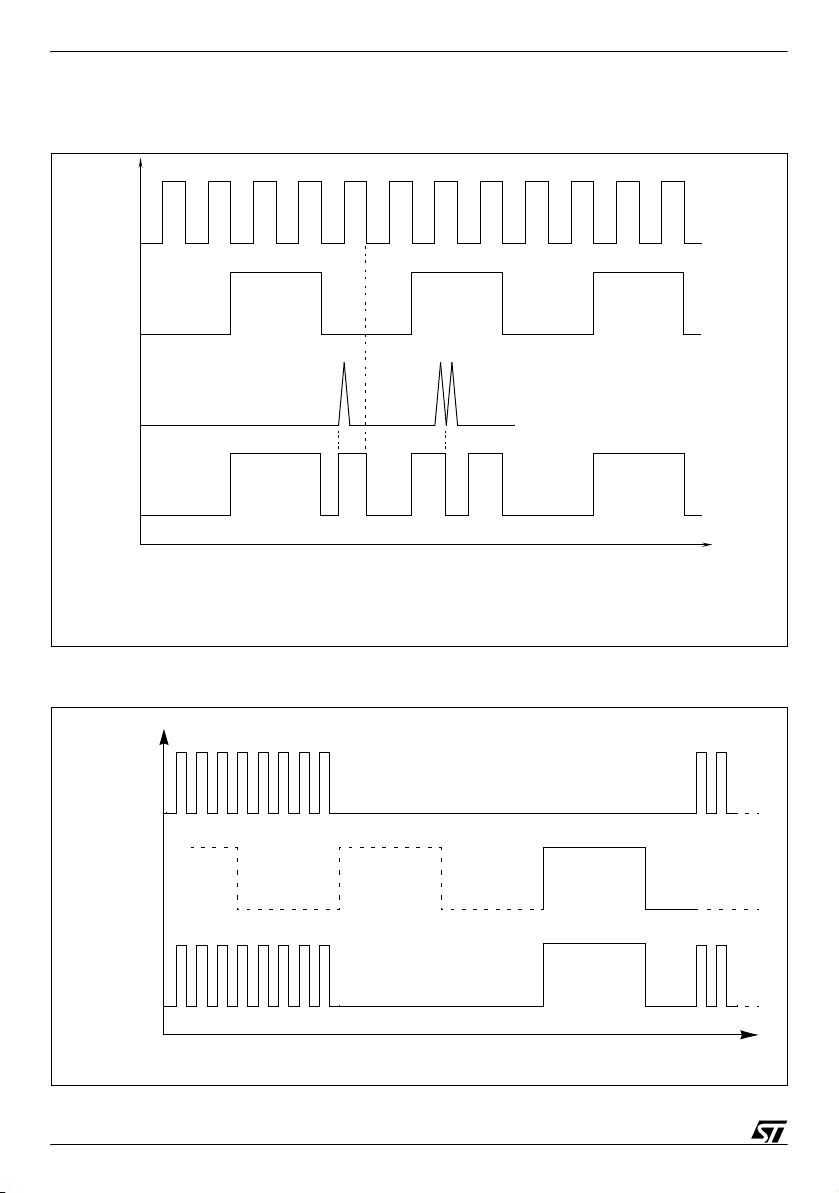
ST6253C ST6263C ST6263B ST6260C ST6260B
(1)
VR001932
(3)
(2)
(4)
(1)
(2)
(3)
(4)
Maximum Frequency for the device to work correctly
Actual Quartz Crystal Frequency at OSCin pin
Noise from OSCin
Resulting Internal Frequency
Main
VR001933
Internal
Emergency
Oscillator
Frequency
Oscillator
CLOCK SYSTEM (Cont’d)
Figure 10. OSG Filtering Principle
Figure 11. OSG Emergency Oscillator Principle
19/83

ST6253C ST6263C ST6263B ST6260C ST6260B
CLOCK SYSTEM (Cont’d)
Oscillator Control Registers
Address: DCh — Write only
Reset State: 00h
7 0
- - - -
Bit 7-4. These bits are not used.
Bit 3. Reserved. Cleared at Reset. Must be kept
cleared.
Bit 2. Reserved. Must be kept low.
RS1-RS0. These bits select the division ratio of
the Oscillator Divider in order to generate the inter
nal frequency. The following selctions are available:
OSCR
3
- RS1 RS0
RS1 RS0 Division Ratio
0
0
1
1
0
1
0
1
Note: Care is required when handling the OSCR
register as some bits are write only. For this rea
son, it is not allowed to change the OSCR contents
while executing interrupt service routine, as the
service routine cannot save and then restore its
previous content. If it is impossible to avoid the
writing of this register in interrupt service routine,
an image of this register must be saved in a RAM
location, and each time the program writes to
-
OSCR it must write also to the image register. The
image register must be written first, so if an inter
rupt occurs between the two instructions the
OSCR is not affected.
1
2
4
4
-
-
20/83
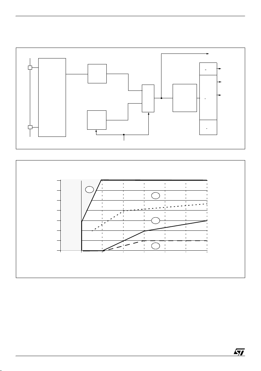
ST6253C ST6263C ST6263B ST6260C ST6260B
MAIN
OSCILLATOR
OSG
LFAO
M
U
X
Core
: 13
:
12
:
1
TIMER 1
Watchdog
POR
f
INT
Main Oscillator off
OSCILLATOR
DIVIDER
RS0,RS1
1
2.5
3.644.555.56
8
7
6
5
4
3
2
Maximum FREQUENCY (MHz)
SUPPLY VOLTAGE (V
DD
)
FUNCTIONALITY IS NOT
3
4
3
2
1
f
OSG
f
OSG
Min (at 85°C)
GUARANTEED
IN THIS AREA
VR01807J
f
OSG
Min (at 125°C)
CLOCK SYSTEM (Cont’d)
Figure 12. Clock Circuit Block Diagram
Figure 13. Maximum Operating Frequency (f
Notes:
1. In this area, operation is guaranteed at the
quartz crystal frequency.
2. When the OSG is disabled, operation in this
area is guaranteed at the crystal frequency. When
the OSG is enabled, operation in this area is guaranteed at a frequency of at least f
3. When the OSG is disabled, operation in this
OSG Min.
MAX
21/83
) versus Supply Voltage (VDD)
area is guaranteed at the quartz crystal frequency.
When the OSG is enabled, access to this area is
prevented. The internal frequency is kept a f
4. When the OSG is disabled, operation in this
area is not guaranteed
When the OSG is enabled, access to this area is
prevented. The internal frequency is kept at f
OSG.
OSG.
ST6253C ST6263C ST6263B ST6260C ST6260B
INT LATCH CLEARED
NMI MASK SET
RESET
( IF PRESENT )
SELECT
NMI MODE FLAGS
IS RESET STILL
PRESENT?
YES
PUT FFEH
ON ADDRESS BUS
FROM RESET LOCATIONS
FFE/FFF
NO
FETCH INSTRUCTION
LOAD PC
VA000427
3.2 RESETS
The MCU can be reset in four ways:
– by the external Reset input being pulled low;
– by Power-on Reset;
– by the digital Watchdog peripheral timing out.
– by Low Voltage Detection (LVD)
3.2.1 RESET Input
The RESET pin may be connected to a device of
the application board in order to reset the MCU if
required. The
RUN, WAIT or STOP mode. This input can be
used to reset the MCU internal state and ensure a
correct start-up procedure. The pin is active low
and features a Schmitt trigger input. The internal
Reset signal is generated by adding a delay to the
external signal. Therefore even short pulses on
RESET pin are acceptable, provided VDD has
the
completed its rising phase and that the oscillator is
running correctly (normal RUN or WAIT modes).
The MCU is kept in the Reset state as long as the
RESET pin is held low.
If RESET activation occurs in the RUN or WAIT
modes, processing of the user program is stopped
(RUN mode only), the Inputs and Outputs are con
figured as inputs with pull-up resistors and the
main Oscillator is restarted. When the level on the
RESET pin then goes high, the initialization se
quence is executed following expiry of the internal
delay period.
If RESET pin activation occurs in the STOP mode,
the oscillator starts up and all Inputs and Outputs
are configured as inputs with pull-up resistors.
When the level of the
the initialization sequence is executed following
expiry of the internal delay period.
3.2.2 Power-on Reset
The function of the POR circuit consists in waking
up the MCU by detecting around 2V a dynamic
(rising edge) variation of the VDD Supply. At the
beginning of this sequence, the MCU is configured
in the Reset state: all I/O ports are configured as
inputs with pull-up resistors and no instruction is
executed. When the power supply voltage rises to
a sufficient level, the oscillator starts to operate,
whereupon an internal delay is initiated, in order to
allow the oscillator to fully stabilize before execut
ing the first instruction. The initialization sequence
RESET pin may be pulled low in
RESET pin then goes high,
is executed immediately following the internal de
lay.
To ensure correct start-up, the user should take
care that the VDD Supply is stabilized at a suffi
cient level for the chosen frequency (see recommended operation) before the reset signal is released. In addition, supply rising must start from
0V.
As a consequence, the POR does not allow to supervise static, slowly rising, or falling, or noisy
(presenting oscillation) VDD supplies.
An external RC network connected to the RESET
pin, or the LVD reset can be used instead to get
the best performances.
Figure 14. Reset and Interrupt Processing
-
-
-
-
-
22/83
ST6253C ST6263C ST6263B ST6260C ST6260B
RESET
RESET
VR02106A
time
V
Up
V
dn
V
DD
RESETS (Cont’d)
3.2.3 Watchdog Reset
The MCU provides a Watchdog timer function in
order to ensure graceful recovery from software
upsets. If the Watchdog register is not refreshed
before an end-of-count condition is reached, the
internal reset will be activated. This, amongst oth
er things, resets the watchdog counter.
The MCU restarts just as though the Reset had
been generated by the
RESET pin, including the
built-in stabilisation delay period.
3.2.4 LVD Reset
The on-chip Low Voltage Detector, selectable as
user option, features static Reset when supply
voltage is below a reference value. Thanks to this
feature, external reset circuit can be removed
while keeping the application safety. This SAFE
RESET is effective as well in Power-on phase as
in power supply drop with different reference val
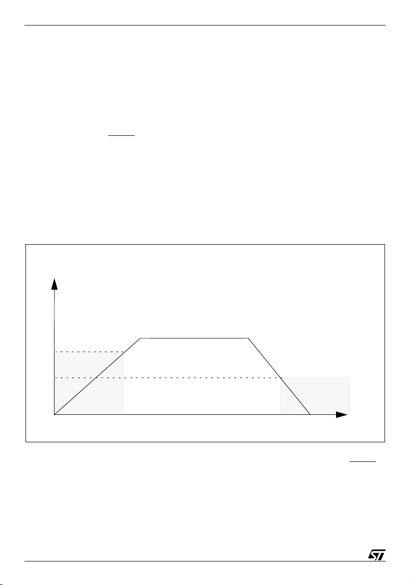
Figure 15. LVD Reset on Power-on and Power-down (Brown-out)
ues, allowing hysteresis effect. Reference value in
case of voltage drop has been set lower than the
reference value for power-on in order to avoid any
parasitic Reset when MCU start's running and
sinking current on the supply.
-
As long as the supply voltage is below the reference value, there is a internal and static RESET
command. The MCU can start only when the sup
ply voltage rises over the reference value. Therefore, only two operating mode exist for the MCU:
RESET active below the voltage reference, and
running mode over the voltage reference as
shown on the Figure 15, that represents a power-
up, power-down sequence.
Note: When the RESET state is controlled by one
of the internal RESET sources (Low Voltage De
tector, Watchdog, Power on Reset), the RESET
pin is tied to low logic level.
-
-
-
3.2.5 Application Notes
No external resistor is required between VDD and
the Reset pin, thanks to the built-in pull-up device.
23/83
Direct external connection of the pin RESET to
must be avoided in order to ensure safe be-
V
DD
haviour of the internal reset sources (AND.Wired
structure).

ST6253C ST6263C ST6263B ST6260C ST6260B
RESET
RESET
VECTOR
JP
JP:2 BYTES/4 CYCLES
RETI
RETI: 1 BYTE/2 CYCLES
INITIALIZATION
ROUTINE
VA00181
V
DD
RESET
R
PU
R
ESD
1)
POWER
WATCHDOG RESET
CK
COUNTER
RESET
ST6
INTERNAL
RESET
f
OSC
RESET
ON RESET
LVD RESET
VR02107A
AND. Wired
1) Resistive ESD protection. Value not guaranteed.
RESETS (Cont’d)
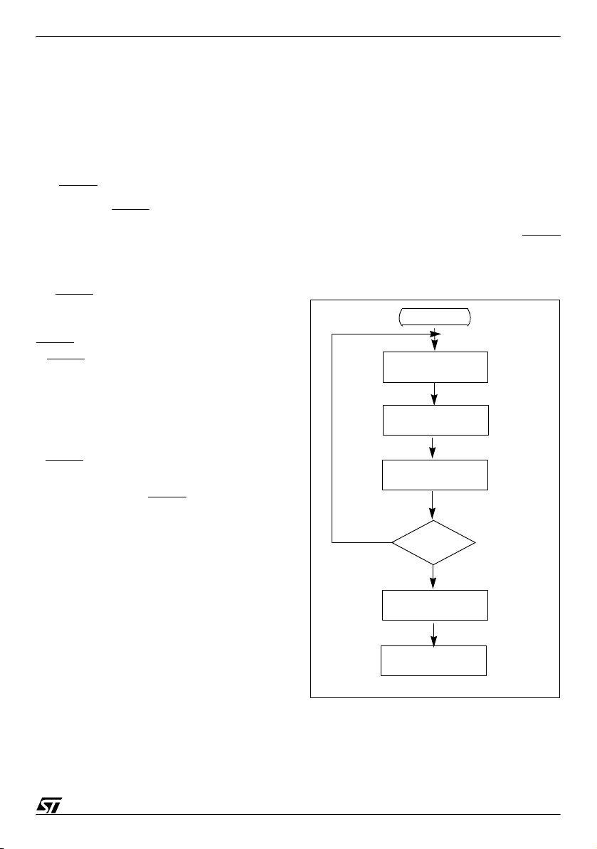
3.2.6 MCU Initialization Sequence
When a reset occurs the stack is reset, the PC is
loaded with the address of the Reset Vector (locat
ed in program ROM starting at address 0FFEh). A
jump to the beginning of the user program must be
coded at this address. Following a Reset, the In
terrupt flag is automatically set, so that the CPU is
in Non Maskable Interrupt mode; this prevents the
initialisation routine from being interrupted. The in
itialisation routine should therefore be terminated
by a RETI instruction, in order to revert to normal
mode and enable interrupts. If no pending interrupt
is present at the end of the initialisation routine, the
MCU will continue by processing the instruction
immediately following the RETI instruction. If, how
ever, a pending interrupt is present, it will be serviced.
Figure 17. Reset Block Diagram
Figure 16. Reset and Interrupt Processing
-
-
-
-
24/83

ST6253C ST6263C ST6263B ST6260C ST6260B
RESETS (Cont’d)
Table 5Register Reset Status
Register Address(es) Status Comment
Oscillator Control Register
EEPROM Control Register
Port Data Registers
Port Direction Register
Port Option Register
Interrupt Option Register
TIMER Status/Control
AR TIMER Mode Control Register
AR TIMER Status/Control 0 Register
AR TIMER Status/Control 1 Register
AR TIMER Compare Register
Miscellaneous Register
SPI Registers
SPI DIV Register
SPI MOD Register
SPI DSR Register
X, Y, V, W, Register
Accumulator
Data RAM
Data RAM Page REgister
Data ROM Window Register
EEPROM
A/D Result Register
AR TIMER Load Register
AR TIMER Reload/Capture Register
0DCh
0EAh
0C0h to 0C2h
0C4h to 0C6h
0CCh to 0CEh
0C8h
0D4h
0D5h
0D6h
0D7h
0DDh
0E0h to 0E2h
0E1h
0E2h
0E0h
080H TO 083H
0FFh
084h to 0BFh
0E8h
0C9h
00h to 03Fh
0D0h
0DBh
0D9h
00h
00h
00h
00h
00h
00h
00h
00h
00h
00h
00h
00h
00h
00h
00h
Undefined
Undefined
EEPROM disabled (if available)
I/O are Input with pull-up
I/O are Input with pull-up
I/O are Input with pull-up
Interrupt disabled
TIMER disabled
AR TIMER stopped
SPI Output not connected to PC3
SPI disabled
SPI disabled
SPI disabled
SPI disabled
As written if programmed
TIMER Counter Register
TIMER Prescaler Register
Watchdog Counter Register
A/D Control Register
25/83
0D3h
0D2h
0D8h
0D1h
FFh
7Fh
FEh
40h
Max count loaded
A/D in Standby

ST6253C ST6263C ST6263B ST6260C ST6260B
3.3 DIGITAL WATCHDOG
The digital Watchdog consists of a reloadable
downcounter timer which can be used to provide
controlled recovery from software upsets.
The Watchdog circuit generates a Reset when the
downcounter reaches zero. User software can
prevent this reset by reloading the counter, and
should therefore be written so that the counter is
regularly reloaded while the user program runs
correctly. In the event of a software mishap (usual
ly caused by externally generated interference),
the user program will no longer behave in its usual
fashion and the timer register will thus not be re
loaded periodically. Consequently the timer will
decrement down to 00h and reset the MCU. In or
der to maximise the effectiveness of the Watchdog
function, user software must be written with this
concept in mind.
Watchdog behaviour is governed by two options,
known as “WATCHDOG ACTIVATION” (i.e.
HARDWARE or SOFTWARE) and “EXTERNAL
STOP MODE CONTROL” (see Table 6).
In the SOFTWARE option, the Watchdog is disabled until bit C of the DWDR register has been set.
Table 6. Recommended Option Choices
Functions Required Recommended Options
Stop Mode & Watchdog “EXTERNAL STOP MODE” & “HARDWARE WATCHDOG”
Stop Mode “SOFTWARE WATCHDOG”
Watchdog “HARDWARE WATCHDOG”
-
-
-
When the Watchdog is disabled, low power Stop
mode is available. Once activated, the Watchdog
cannot be disabled, except by resetting the MCU.
In the HARDWARE option, the Watchdog is permanently enabled. Since the oscillator will run continuously, low power mode is not available. The
STOP instruction is interpreted as a WAIT instruc
tion, and the Watchdog continues to countdown.
However, when the EXTERNAL STOP MODE
CONTROL option has been selected low power
consumption may be achieved in Stop Mode.
Execution of the STOP instruction is then governed by a secondary function associated with the
NMI pin. If a STOP instruction is encountered
when the NMI pin is low, it is interpreted as WAIT,
as described above. If, however, the STOP in
struction is encountered when the NMI pin is high,
the Watchdog counter is frozen and the CPU en
ters STOP mode.
When the MCU exits STOP mode (i.e. when an interrupt is generated), the Watchdog resumes its
activity.
-
-
-
26/83

ST6253C ST6263C ST6263B ST6260C ST6260B
WATCHDOG CONTROL REGISTER
D0
D1
D3
D4
D5
D6
D7
WATCHDOG COUNTER
C
SR
T5
T4
T3
T2
T1
D2
T0
OSC ÷12
RESET
VR02068A
÷2
8
DIGITAL WATCHDOG (Cont’d)
The Watchdog is associated with a Data space
register (Digital WatchDog Register, DWDR, loca
tion 0D8h) which is described in greater detail in
Section 3.3.1 Digital Watchdog Register (DWDR).
This register is set to 0FEh on Reset: bit C is
cleared to “0”, which disables the Watchdog; the
timer downcounter bits, T0 to T5, and the SR bit
are all set to “1”, thus selecting the longest Watch
dog timer period. This time period can be set to the
user’s requirements by setting the appropriate val
ue for bits T0 to T5 in the DWDR register. The SR
bit must be set to “1”, since it is this bit which gen
erates the Reset signal when it changes to “0”;
clearing this bit would generate an immediate Re
set.
It should be noted that the order of the bits in the
DWDR register is inverted with respect to the as
sociated bits in the down counter: bit 7 of the
DWDR register corresponds, in fact, to T0 and bit
2 to T5. The user should bear in mind the fact that
these bits are inverted and shifted with respect to
the physical counter bits when writing to this regis
ter. The relationship between the DWDR register
bits and the physical implementation of the Watch
dog timer downcounter is illustrated in Figure 18.
Only the 6 most significant bits may be used to define the time period, since it is bit 6 which triggers
the Reset when it changes to “0”. This offers the
user a choice of 64 timed periods ranging from
3,072 to 196,608 clock cycles (with an oscillator
frequency of 8
MHz, this is equivalent to timer peri-
ods ranging from 384 µs to 24.576 ms).
-
-
-
-
-
-
-
-
Figure 18. Watchdog Counter Control
27/83

ST6253C ST6263C ST6263B ST6260C ST6260B
DIGITAL WATCHDOG (Cont’d)
3.3.1 Digital Watchdog Register (DWDR)
Address: 0D8h — Read/Write
Reset status: 1111 1110 b
7 0
T0 T1 T2 T3 T4 T5 SR C
Bit 0 = C: Watchdog Control bit
If the hardware option is selected, this bit is forced
high and the user cannot change it (the Watchdog
is always active). When the software option is se
lected, the Watchdog function is activated by setting bit C to 1, and cannot then be disabled (save
by resetting the MCU).
When C is kept low the counter can be used as a
7-bit timer.
This bit is cleared to “0” on Reset.
Bit 1 = SR: Software Reset bit
This bit triggers a Reset when cleared.
When C = “0” (Watchdog disabled) it is the MSB of
the 7-bit timer.
This bit is set to “1” on Reset.
Bits 2-7 = T5-T0: Downcounter bits
It should be noted that the register bits are reversed and shifted with respect to the physical
counter: bit-7 (T0) is the LSB of the Watchdog
downcounter and bit-2 (T5) is the MSB.
These bits are set to “1” on Reset.
3.3.2 Application Notes
The Watchdog plays an important supporting role
in the high noise immunity of ST62xx devices, and
should be used wherever possible. Watchdog re
lated options should be selected on the basis of a
trade-off between application security and STOP
mode availability.
When STOP mode is not required, hardware activation without EXTERNAL STOP MODE CONTROL should be preferred, as it provides maximum security, especially during power-on.
When STOP mode is required, hardware activa-
tion and EXTERNAL STOP MODE CONTROL
should be chosen. NMI should be high by default,
to allow STOP mode to be entered when the MCU
is idle.
The NMI pin can be connected to an I/O line (see
Figure 19) to allow its state to be controlled by soft
ware. The I/O line can then be used to keep NMI
low while Watchdog protection is required, or to
avoid noise or key bounce. When no more
processing is required, the I/O line is released and
the device placed in STOP mode for lowest power
consumption.
When software activation is selected and the
Watchdog is not activated, the downcounter may
be used as a simple 7-bit timer (remember that the
bits are in reverse order).
The software activation option should be chosen
only when the Watchdog counter is to be used as
a timer. To ensure the Watchdog has not been un
expectedly activated, the following instructions
should be executed within the first 27 instructions:
jrr 0, WD, #+3
ldi WD, 0FDH
-
-
-
28/83

ST6253C ST6263C ST6263B ST6260C ST6260B
NMI
SWITCH
I/O
VR02002
RSFF
8
DATA BUS
VA00010
-2
-12
OSCILLATOR
RESET
WRITE
RESET
DB0
R
S
Q
DB1.7 SETLOAD
7
8
-2
SET
CLOCK
DIGITAL WATCHDOG (Cont’d)
These instructions test the C bit and Reset the
MCU (i.e. disable the Watchdog) if the bit is set
(i.e. if the Watchdog is active), thus disabling the
Watchdog.
In all modes, a minimum of 28 instructions are executed after activation, before the Watchdog can
generate a Reset. Consequently, user software
should load the watchdog counter within the first
27 instructions following Watchdog activation
(software mode), or within the first 27 instructions
executed following a Reset (hardware activation).
It should be noted that when the GEN bit is low (interrupts disabled), the NMI interrupt is active but
cannot cause a wake up from STOP/WAIT modes.
Figure 20. Digital Watchdog Block Diagram
Figure 19. A typical circuit making use of the
EXERNAL STOP MODE CONTROL feature
29/83

ST6253C ST6263C ST6263B ST6260C ST6260B
3.4 INTERRUPTS
The CPU can manage four Maskable Interrupt
sources, in addition to a Non Maskable Interrupt
source (top priority interrupt). Each source is asso
ciated with a specific Interrupt Vector which contains a Jump instruction to the associated interrupt
service routine. These vectors are located in Pro
gram space (see Table 7).
When an interrupt source generates an interrupt
request, and interrupt processing is enabled, the
PC register is loaded with the address of the inter
rupt vector (i.e. of the Jump instruction), which
then causes a Jump to the relevant interrupt serv
ice routine, thus servicing the interrupt.
Interrupt sources are linked to events either on external pins, or on chip peripherals. Several events
can be ORed on the same interrupt source, and
relevant flags are available to determine which
event triggered the interrupt.
The Non Maskable Interrupt request has the highest priority and can interrupt any interrupt routine
at any time; the other four interrupts cannot inter
rupt each other. If more than one interrupt request
is pending, these are processed by the processor
core according to their priority level: source #1 has
the higher priority while source #4 the lower. The
priority of each interrupt source is fixed.
Table 7. Interrupt Vector Map
Interrupt Source Priority Vector Address
Interrupt source #0 1 (FFCh-FFDh)
Interrupt source #1 2 (FF6h-FF7h)
Interrupt source #2 3 (FF4h-FF5h)
Interrupt source #3 4 (FF2h-FF3h)
Interrupt source #4 5 (FF0h-FF1h)
3.4.1 Interrupt request
All interrupt sources but the Non Maskable Interrupt source can be disabled by setting accordingly
the GEN bit of the Interrupt Option Register (IOR).
This GEN bit also defines if an interrupt source, in
cluding the Non Maskable Interrupt source, can restart the MCU from STOP/WAIT modes.
Interrupt request from the Non Maskable Interrupt
source #0 is latched by a flip flop which is automat
ically reset by the core at the beginning of the nonmaskable interrupt service routine.
-
Interrupt request from source #1 can be configured either as edge or level sensitive by setting accordingly the LES bit of the Interrupt Option Regis-
-
ter (IOR).
Interrupt request from source #2 are always edge
sensitive. The edge polarity can be configured by
setting accordingly the ESB bit of the Interrupt Op
-
tion Register (IOR).
Interrupt request from sources #3 & #4 are level
sensitive.
In edge sensitive mode, a latch is set when a edge
occurs on the interrupt source line and is cleared
when the associated interrupt routine is started.
So, the occurrence of an interrupt can be stored,
until completion of the running interrupt routine be
fore being processed. If several interrupt requests
occurs before completion of the running interrupt
routine, only the first request is stored.
Storage of interrupt requests is not available in lev-
el sensitive mode. To be taken into account, the
low level must be present on the interrupt pin when
the MCU samples the line after instruction execu
tion.
At the end of every instruction, the MCU tests the
interrupt lines: if there is an interrupt request the
next instruction is not executed and the appropri
ate interrupt service routine is executed instead.
Table 8. Interrupt Option Register Description
GEN
ESB
LES
-
OTHERS NOT USED
SET Enable all interrupts
CLEARED Disable all interrupts
SET
CLEARED
SET
CLEARED
Rising edge mode on interrupt source #2
Falling edge mode on interrupt source #2
Level-sensitive mode on interrupt source #1
Falling edge mode on interrupt source #1
-
-
-
-
-
30/83

ST6253C ST6263C ST6263B ST6260C ST6260B
INSTRUCTION
FETCH
INSTRUCTION
EXECUTE
INSTRUCTION
WAS
THE INSTRUCTION
A RETI
?
?
CLEAR
INTERRUPT MASK
SELECT
PROGRAM FLAGS
"POP"
THE STACKED PC
?
CHECK IF THERE IS
AN INTERRUPT REQUEST
AND INTERRUPT MASK
SELECT
INTERNAL MODE FLAG
PUSH THE
PC INTO THE STACK
LOAD PC FROM
INTERRUPT VECTOR
(FFC/FFD)
SET
INTERRUPT MASK
NO
NO
YES
IS THE CORE
ALREADY IN
NORMAL MODE?
VA000014
YES
NO
YES
INTERRUPTS (Cont’d)
3.4.2 Interrupt Procedure
The interrupt procedure is very similar to a call procedure, indeed the user can consider the interrupt
as an asynchronous call procedure. As this is an
asynchronous event, the user cannot know the
context and the time at which it occurred. As a re
sult, the user should save all Data space registers
which may be used within the interrupt routines.
There are separate sets of processor flags for nor
mal, interrupt and non-maskable interrupt modes,
which are automatically switched and so do not
need to be saved.
The following list summarizes the interrupt procedure:
MCU
– The interrupt is detected.
– The C and Z flags are replaced by the interrupt
flags (or by the NMI flags).
– The PC contents are stored in the first level of
the stack.
– The normal interrupt lines are inhibited (NMI still
active).
– The first internal latch is cleared.
– The associated interrupt vector is loaded in the PC.
WARNING: In some circumstances, when a
maskable interrupt occurs while the ST6 core is in
NORMAL mode and especially during the execu
tion of an "ldi IOR, 00h" instruction (disabling all
maskable interrupts): if the interrupt arrives during
the first 3 cycles of the "ldi" instruction (which is a
4-cycle instruction) the core will switch to interrupt
mode BUT the flags CN and ZN will NOT switch to
the interrupt pair CI and ZI.
User
– User selected registers are saved within the in-
terrupt service routine (normally on a software
stack).
– The source of the interrupt is found by polling the
interrupt flags (if more than one source is associ
ated with the same vector).
– The interrupt is serviced.
– Return from interrupt (RETI)
MCU
– Automatically the MCU switches back to the nor-
mal flag set (or the interrupt flag set) and pops
the previous PC value from the stack.
The interrupt routine usually begins by the identify-
-
ing the device which generated the interrupt request (by polling). The user should save the registers which are used within the interrupt routine in a
-
software stack. After the RETI instruction is exe
cuted, the MCU returns to the main routine.
Figure 21. Interrupt Processing Flow Chart
-
-
-
31/83

ST6253C ST6263C ST6263B ST6260C ST6260B
INTERRUPTS (Cont’d)
3.4.3 Interrupt Option Register (IOR)
The Interrupt Option Register (IOR) is used to enable/disable the individual interrupt sources and to
select the operating mode of the external interrupt
inputs. This register is write-only and cannot be
accessed by single-bit operations.
Address: 0C8h — Write Only
Reset status: 00h
7 0
- LES ESB GEN - - - -
Bit 7, Bits 3-0 = Unused.
Bit 6 = LES: Level/Edge Selection bit.
When this bit is set to one, the interrupt source #1
is level sensitive. When cleared to zero the edge
sensitive mode for interrupt request is selected.
Table 9Interrupt Requests and Mask Bits
Peripheral Register
GENERAL IOR C8h GEN All Interrupts, excluding NMI
TIMER TSCR1 D4h ETI TMZ: TIMER Overflow Vector 4
A/D CONVERTER ADCR D1h EAI EOC: End of Conversion Vector 4
AR TIMER ARMC D5h
SPI SPIMOD E2h SPIE SPRUN: End of Transmission Vector 2
Port PAn ORPA-DRPA C0h-C4h ORPAn-DRPAn PAn pin Vector 1
Port PBn ORPB-DRPB C1h-C5h ORPBn-DRPBn PBn pin Vector 1
Port PCn ORPC-DRPC C2h-C6h ORPCn-DRPCn PCn pin Vector 2
Address
Register
Bit 5 = ESB: Edge Selection bit.
The bit ESB selects the polarity of the interrupt
source #2.
Bit 4 = GEN: Global Enable Interrupt. When this bit
is set to one, all interrupts are enabled. When this
bit is cleared to zero all the interrupts (excluding
NMI) are disabled.
When the GEN bit is low, the NMI interrupt is active but cannot cause a wake up from STOP/WAIT
modes.
This register is cleared on reset.
3.4.4 Interrupt sources
Interrupt sources available on these MCUs are
summarized in the
bit to enable/disable the interrupt request.
Mask bit Masked Interrupt Source
OVIE
CPIE
EIE
Table 9 with associated mask
OVF: AR TIMER Overflow
CPF: Successful compare
EF: Active edge on ARTIMin
Interrupt
vector
Vector 3
32/83

ST6253C ST6263C ST6263B ST6260C ST6260B
Start
1
I
QCLK
CLR
FF
1
0
MUX
IOR REG. C8H, bit 6
IOR REG. C8H, bit 5
FF
CLR
CLK Q
I
2
Start
TIMER1
CPIE
CPF
TMZ
ETI
INT #4 (FF0,1)
INT #3 (FF2,3)
INT #2 (FF4,5)
INT #1 (FF6,7)
RESTART FROM
STOP/WAIT
AR TIMER
EF
EIE
OVF
OVIE
VA0426K
PBE
Bits
Bits
PORT B
PORT A
PBE
PBE
DD
V
SINGLE BIT ENABLE
FROM REGISTER PORT A,B,C
PORT C
SPINT bit
Start
0
I
QCLK
CLR
FF
Bit GEN (IOR Register)
NMI (FFC,D)
NMI
V
DD
ADC
EOC
EAI
SPIE bit
SPIDIV Register
SPIMOD Register
INTERRUPTS (Cont’d)
Figure 22. Interrupt Block Diagram
33/83

ST6253C ST6263C ST6263B ST6260C ST6260B
3.5 POWER SAVING MODES
The WAIT and STOP modes have been implemented in the ST62xx family of MCUs in order to
reduce the product’s electrical consumption during
idle periods. These two power saving modes are
described in the following paragraphs.
3.5.1 WAIT Mode
The MCU goes into WAIT mode as soon as the
WAIT instruction is executed. The microcontroller
can be considered as being in a “software frozen”
state where the core stops processing the pro
gram instructions, the RAM contents and peripheral registers are preserved as long as the power
supply voltage is higher than the RAM retention
voltage. In this mode the peripherals are still ac
tive.
WAIT mode can be used when the user wants to
reduce the MCU power consumption during idle
periods, while not losing track of time or the capability of monitoring external events. The active oscillator is not stopped in order to provide a clock
signal to the peripherals. Timer counting may be
enabled as well as the Timer interrupt, before en
tering the WAIT mode: this allows the WAIT mode
to be exited when a Timer interrupt occurs. The
same applies to other peripherals which use the
clock signal.
If the WAIT mode is exited due to a Reset (either
by activating the external pin or generated by the
Watchdog), the MCU enters a normal reset proce
dure. If an interrupt is generated during WAIT
mode, the MCU’s behaviour depends on the state
of the processor core prior to the WAIT instruction,
but also on the kind of interrupt request which is
generated. This is described in the following para
graphs. The processor core does not generate a
delay following the occurrence of the interrupt, because the oscillator clock is still available and no
stabilisation period is necessary.
3.5.2 STOP Mode
If the Watchdog is disabled, STOP mode is availa-
-
ble. When in STOP mode, the MCU is placed in
the lowest power consumption mode. In this operating mode, the microcontroller can be considered
as being “frozen”, no instruction is executed, the
oscillator is stopped, the RAM contents and pe
ripheral registers are preserved as long as the
power supply voltage is higher than the RAM re
tention voltage, and the ST62xx core waits for the
occurrence of an external interrupt request or a
Reset to exit the STOP state.
If the STOP state is exited due to a Reset (by activating the external pin) the MCU will enter a nor-
-
mal reset procedure. Behaviour in response to interrupts depends on the state of the processor
core prior to issuing the STOP instruction, and
also on the kind of interrupt request that is gener
ated.
This case will be described in the following paragraphs. The processor core generates a delay af-
-
ter occurrence of the interrupt request, in order to
wait for complete stabilisation of the oscillator, before executing the first instruction.
-
-
-
-
34/83

ST6253C ST6263C ST6263B ST6260C ST6260B
POWER SAVING MODE (Cont’d)
3.5.3 Exit from WAIT and STOP Modes
The following paragraphs describe how the MCU
exits from WAIT and STOP modes, when an interrupt occurs (not a Reset). It should be noted that
the restart sequence depends on the original state
of the MCU (normal, interrupt or non-maskable interrupt mode) prior to entering WAIT or STOP
mode, as well as on the interrupt type.
Interrupts do not affect the oscillator selection.
3.5.3.1 Normal Mode
If the MCU was in the main routine when the WAIT
or STOP instruction was executed, exit from Stop
or Wait mode will occur as soon as an interrupt occurs; the related interrupt routine is executed and,
on completion, the instruction which follows the
STOP or WAIT instruction is then executed, providing no other interrupts are pending.
3.5.3.2 Non Maskable Interrupt Mode
If the STOP or WAIT instruction has been executed during execution of the non-maskable interrupt
routine, the MCU exits from the Stop or Wait mode
as soon as an interrupt occurs: the instruction
which follows the STOP or WAIT instruction is ex
ecuted, and the MCU remains in non-maskable interrupt mode, even if another interrupt has been
generated.
3.5.3.3 Normal Interrupt Mode
If the MCU was in interrupt mode before the STOP
or WAIT instruction was executed, it exits from
STOP or WAIT mode as soon as an interrupt oc
curs. Nevertheless, two cases must be considered:
– If the interrupt is a normal one, the interrupt rou-
tine in which the WAIT or STOP mode was en-
-
-
tered will be completed, starting with the
execution of the instruction which follows the
STOP or the WAIT instruction, and the MCU is
still in the interrupt mode. At the end of this rou
tine pending interrupts will be serviced in accordance with their priority.
– In the event of a non-maskable interrupt, the
non-maskable interrupt service routine is proc
essed first, then the routine in which the WAIT or
STOP mode was entered will be completed by
executing the instruction following the STOP or
WAIT instruction. The MCU remains in normal
interrupt mode.
Notes:
To achieve the lowest power consumption during
RUN or WAIT modes, the user program must take
care of:
– configuring unused I/Os as inputs without pull-up
(these should be externally tied to well defined
logic levels);
– placing all peripherals in their power down
modes before entering STOP mode;
When the hardware activated Watchdog is selected, or when the software Watchdog is enabled, the
STOP instruction is disabled and a WAIT instruction will be executed in its place.
If all interrupt sources are disabled (GEN low), the
MCU can only be restarted by a Reset. Although
setting GEN low does not mask the NMI as an in
terrupt, it will stop it generating a wake-up signal.
The WAIT and STOP instructions are not executed if an enabled interrupt request is pending.
-
-
-
35/83

ST6253C ST6263C ST6263B ST6260C ST6260B
V
DD
RESET
SIN CONTROLS
S
OUT
SHIFT
REGISTER
DATA
DATA
DIRECTION
REGISTER
REGISTER
OPTION
REGISTER
INPUT/OUTPUT
TO INTERRUPT
V
DD
TO ADC
VA00413
4 ON-CHIP PERIPHERALS
4.1 I/O PORTS
The MCU features Input/Output lines which may
be individually programmed as any of the following
input or output configurations:
– Input without pull-up or interrupt
– Input with pull-up and interrupt
– Input with pull-up, but without interrupt
– Analog input
– Push-pull output
– Open drain output
The lines are organised as bytewise Ports.
Each port is associated with 3 registers in Data
space. Each bit of these registers is associated
with a particular line (for instance, bits 0 of Port A
Data, Direction and Option registers are associat
ed with the PA0 line of Port A).
The DATA registers (DRx), are used to read the
voltage level values of the lines which have been
configured as inputs, or to write the logic value of
the signal to be output on the lines configured as
outputs. The port data registers can be read to get
the effective logic levels of the pins, but they can
Figure 23. I/O Port Block Diagram
be also written by user software, in conjunction
with the related option registers, to select the dif
ferent input mode options.
Single-bit operations on I/O registers are possible
but care is necessary because reading in input
mode is done from I/O pins while writing will direct
ly affect the Port data register causing an undesired change of the input configuration.
The Data Direction registers (DDRx) allow the
data direction (input or output) of each pin to be
set.
The Option registers (ORx) are used to select the
different port options available both in input and in
output mode.
All I/O registers can be read or written to just as
any other RAM location in Data space, so no extra
RAM cells are needed for port data storage and
manipulation. During MCU initialization, all I/O reg
isters are cleared and the input mode with pull-ups
and no interrupt generation is selected for all the
pins, thus avoiding pin conflicts.
-
-
-
36/83

ST6253C ST6263C ST6263B ST6260C ST6260B
I/O PORTS (Cont’d)
4.1.1 Operating Modes
Each pin may be individually programmed as input
or output with various configurations.
This is achieved by writing the relevant bit in the
Data (DR), Data Direction (DDR) and Option reg
isters (OR). Table 10 illustrates the various port
configurations which can be selected by user soft
ware.
4.1.1.1 Input Options
Pull-up, High Impedance Option. All input lines
can be individually programmed with or without an
internal pull-up by programming the OR and DR
registers accordingly. If the pull-up option is not
selected, the input pin will be in the high-imped
ance state.
Table 10. I/O Port Option Selection
DDR OR DR Mode Option
0 0 0 Input With pull-up, no interrupt
0 0 1 Input No pull-up, no interrupt
0 1 0 Input With pull-up and with interrupt
0 1 1 Input Analog input (when available)
1 0 X Output Open-drain output (20mA sink when available)
1 1 X Output Push-pull output (20mA sink when available)
Note: X = Don’t care
4.1.1.2 Interrupt Options
All input lines can be individually connected by
software to the interrupt system by programming
the OR and DR registers accordingly. The inter
rupt trigger modes (falling edge, rising edge and
low level) can be configured by software as de
scribed in the Interrupt Chapter for each port.
-
4.1.1.3 Analog Input Options
Some pins can be configured as analog inputs by
programming the OR and DR registers according
ly. These analog inputs are connected to the onchip 8-bit Analog to Digital Converter. ONLY ONE
pin should be programmed as an analog input at
any time, since by selecting more than one input
simultaneously their pins will be effectively short
ed.
-
-
-
-
37/83

ST6253C ST6263C ST6263B ST6260C ST6260B
Interrupt
pull-up
Output
Open Drain
Output
Push-pull
Input
pull-up (Reset
state)
Input
Analog
Output
Open Drain
Output
Push-pull
Input
010*
000
100
110
011
001
101
111
I/O PORTS (Cont’d)
4.1.2 Safe I/O State Switching Sequence
Switching the I/O ports from one state to another
should be done in a sequence which ensures that
no unwanted side effects can occur. The recom
mended safe transitions are illustrated in Figure
24. All other transitions are potentially risky and
should be avoided when changing the I/O operat
ing mode, as it is most likely that undesirable sideeffects will be experienced, such as spurious inter
rupt generation or two pins shorted together by the
analog multiplexer.
Single bit instructions (SET, RES, INC and DEC)
should be used with great caution on Ports Data
registers, since these instructions make an implicit
read and write back of the entire register. In port
input mode, however, the data register reads from
the input pins directly, and not from the data regis
ter latches. Since data register information in input
mode is used to set the characteristics of the input
pin (interrupt, pull-up, analog input), these may be
unintentionally reprogrammed depending on the
state of the input pins. As a general rule, it is better
to limit the use of single bit instructions on data
registers to when the whole (8-bit) port is in output
mode. In the case of inputs or of mixed inputs and
Figure 24. Diagram showing Safe I/O State Transitions
outputs, it is advisable to keep a copy of the data
register in RAM. Single bit instructions may then
be used on the RAM copy, after which the whole
copy register can be written to the port data regis
ter:
SET bit, datacopy
LD a, datacopy
-
LD DRA, a
Warning: Care must also be taken to not use in-
structions that act on a whole port register (INC,
DEC, or read operations) when all 8 bits are not
available on the device. Unavailable bits must be
masked by software (AND instruction).
The WAIT and STOP instructions allow the
ST62xx to be used in situations where low power
consumption is needed. The lowest power con
sumption is achieved by configuring I/Os in input
mode with well-defined logic levels.
The user must take care not to switch outputs with
heavy loads during the conversion of one of the
analog inputs in order to avoid any disturbance to
the conversion.
-
-
Note *. xxx = DDR, OR, DR Bits respectively
38/83

ST6253C ST6263C ST6263B ST6260C ST6260B
Data in
Interrupt
Data in
Interrupt
Data in
Interrupt
Data out
ADC
Data out
I/O PORTS (Cont’d)
Table 11I/O Port Option Selections
MODE AVAILABLE ON
PA0-PA3
Input
PB0-PB3, PB6-PB7
PC2-PC4
(1)
SCHEMATIC
Input
with pull up
Input
with pull up
with interrupt
Analog Input
Open drain output
5mA
Open drain output
30mA
Push-pull output
5mA
Push-pull output
30mA
PA0-PA3
PB0-PB3, PB6-PB7
PC2-PC4
PA0-PA3
PB0-PB3, PB6-PB7
PC2-PC4
PA0-PA3
PC2-PC4
PA0-PA3
PC2-PC4
PB0-PB3, PB6-PB7
PA0-PA3
PC2-PC4
PB0-PB3, PB6-PB7
Note 1. Provided the correct configuration has been selected.
39/83

ST6253C ST6263C ST6263B ST6260C ST6260B
I/O PORTS (Cont’d)
4.1.3 AR Timer Alternate function Option
When bit PWMOE of register ARMC is low, pin ARTIMout/PB7 is configured as any standard pin of
port B through the port registers. When PWMOE is
high, ARTIMout/PB7 is the PWM output, independ
ently of the port registers configuration.
ARTIMin/PB6 is connected to the AR Timer input.
It is configured through the port registers as any
standard pin of port B. To use ARTIMin/PB6 as AR
Timer input, it must be configured as input through
DDRB.
4.1.4 SPI Alternate function Option
PC2/PC4 are used as standard I/O as long as bit
SPCLK of the SPI Mode Register is kept low.
When PC2/Sin is configured as input, it is automat
-
ically connected to the SPI shift register input, independent of the state at SPCLK.
PC3/SOUT is configured as SPI push-pull output
by setting bit 0 of the Miscellaneous register (ad
dress DDh), regardless of the state of Port C registers. PC4/SCK is configured as push-pull output
clock (master mode) by programming it as pushpull output through DDRC register and by setting
bit SPCLK of the SPI Mode Register.
PC4/SCK is configured as input clock (slave mode)
by programming it as input through DDRC register
and by clearing bit SPCLK of the SPI Mode Regis
ter. With this configuration, PC4 can simultaneously be used as an input.
-
-
-
40/83

ST6253C ST6263C ST6263B ST6260C ST6260B
MUX
1
0
DR
PP/OD
OUT
IN
CLOCK IN
SPI
DR
DR
0
1
MUX
IN
OUT
TIMER 1
DR
MUX
1
0
DR
OR
AR TIMER
ARTIMout
ARTIMin
PWMOE
PP/OD
PC3/Sout
PC2/Sin
PC4/SCK
PC1/TIM1
ARTIMin
ARTIMout
VR0C1661
V
DD
b0
REGISTER
MISC.
0
1
CLOCK OUT
SPCLK
MOD REGISTER
MUX
OR
OR
DR
OR
TOUT
I/O PORTS (Cont’d)
Figure 25Peripheral Interface Configuration of SPI, Timer 1 and AR Timer
41/83

ST6253C ST6263C ST6263B ST6260C ST6260B
DATA BUS
8-BIT
COUNTER
STATUS/CONTROL
REGISTER
INTERRUPT
LINE
VR02070A
3
8
8
8
6
5
4
3
2
1
0
SELECT
1 OF 7
12
b7 b6 b5 b4 b3 b2 b1 b0
TMZ ETI D5 D4 PSI PS2 PS1 PS0
f
INT
PSC
4.2 TIMER
The MCU features an on-chip Timer peripheral,
consisting of an 8-bit counter with a 7-bit program
mable prescaler, giving a maximum count of 215.
Figure 26 shows the Timer Block Diagram. The
content of the 8-bit counter can be read/written in
the Timer/Counter register, TCR, which can be ad
dressed in Data space as a RAM location at address 0D3h. The state of the 7-bit prescaler can be
read in the PSC register at address 0D2h. The
control logic device is managed in the TSCR reg
ister as described in the following paragraphs.
The 8-bit counter is decrement by the output (rising edge) coming from the 7-bit prescaler and can
be loaded and read under program control. When
it decrements to zero then the TMZ (Timer Zero)bit
in the TSCR is set. If the ETI (Enable Timer Inter
rupt) bit in the TSCR is also set, an interrupt request is generated. The Timer interrupt can be
used to exit the MCU from WAIT mode.
Figure 26. Timer Block Diagram
The prescaler input is the internal frequency (f
-
divided by 12. The prescaler decrements on the
rising edge. Depending on the division factor pro
grammed by PS2, PS1 and PS0 bits in the TSCR
(see Figure 12), the clock input of the timer/coun
ter register is multiplexed to different sources. For
division factor 1, the clock input of the prescaler is
also that of timer/counter; for factor 2, bit 0 of the
prescaler register is connected to the clock input of
TCR. This bit changes its state at half the frequen
cy of the prescaler input clock. For factor 4, bit 1 of
the PSC is connected to the clock input of TCR,
and so forth. The prescaler initialize bit, PSI, in the
TSCR register must be set to allow the prescaler
(and hence the counter) to start. If it is cleared, all
the prescaler bits are set and the counter is inhib
-
ited from counting. The prescaler can be loaded
with any value between 0 and 7Fh, if bit PSI is set.
The prescaler tap is selected by means of the
PS2/PS1/PS0 bits in the control register.
Figure 27 illustrates the Timer’s working principle.
INT
)
-
-
-
-
42/83

ST6253C ST6263C ST6263B ST6260C ST6260B
BIT0
BIT1 BIT2
BIT3 BIT6BIT5BIT4
CLOCK
7-BIT PRESCALER
8-1 MULTIPLEXER
8-BIT COUNTER
BIT0 BIT1
BIT2
BIT3 BIT4 BIT5
BIT6
BIT7
10234
5
6
7
PS0
PS1
PS2
VA00186
TIMER (Cont’d)
4.2.1 Timer Operation
The Timer prescaler is clocked by the prescaler
clock input (f
The user can select the desired prescaler division
ratio through the PS2, PS1, PS0 bits. When the
TCR count reaches 0, it sets the TMZ bit in the
TSCR. The TMZ bit can be tested under program
control to perform a timer function whenever it
goes high.
4.2.2 Timer Interrupt
When the counter register decrements to zero with
the ETI (Enable Timer Interrupt) bit set to one, an
interrupt request associated with Interrupt Vector
#4 is generated. When the counter decrements to
Figure 27. Timer Working Principle
INT
÷ 12).
zero, the TMZ bit in the TSCR register is set to
one.
4.2.3 Application Notes
TMZ is set when the counter reaches zero; however, it may also be set by writing 00h in the TCR
register or by setting bit 7 of the TSCR register.
The TMZ bit must be cleared by user software
when servicing the timer interrupt to avoid unde
sired interrupts when leaving the interrupt service
routine. After reset, the 8-bit counter register is
loaded with 0FFh, while the 7-bit prescaler is load
ed with 07Fh, and the TSCR register is cleared.
This means that the Timer is stopped (PSI=“0”)
and the timer interrupt is disabled.
-
-
43/83

ST6253C ST6263C ST6263B ST6260C ST6260B
TIMER (Cont’d)
A write to the TCR register will predominate over
the 8-bit counter decrement to 00h function, i.e. if a
write and a TCR register decrement to 00h occur
simultaneously, the write will take precedence,
and the TMZ bit is not set until the 8-bit counter
reaches 00h again. The values of the TCR and the
PSC registers can be read accurately at any time.
4.2.4 Timer Registers Timer Status Control Register (TSCR)
Address: 0D4h — Read/Write
7 0
TMZ ETI D5 D4 PSI PS2 PS1 PS0
Bit 7 = TMZ: Timer Zero bit
A low-to-high transition indicates that the timer
count register has decrement to zero. This bit
must be cleared by user software before starting a
new count.
Bit 6 = ETI: Enable Timer Interrup
When set, enables the timer interrupt request
(vector #4). If ETI=0 the timer interrupt is disabled.
If ETI=1 and TMZ=1 an interrupt request is gener
ated.
Bit 5 = D5: Reserved
Must be set to “1”.
Bit 4 = D4
Do not care.
Bit 3 = PSI: Prescaler Initialize Bit
Used to initialize the prescaler and inhibit its count-
ing. When PSI=“0” the prescaler is set to 7Fh and
the counter is inhibited. When PSI=“1” the prescal
er is enabled to count downwards. As long as
PSI=“0” both counter and prescaler are not run
ning.
Bit 2, 1, 0 = PS2, PS1, PS0: Prescaler Mux. Select. These bits select the division ratio of the pres-
caler register.
Table 12. Prescaler Division Factors
PS2 PS1 PS0 Divided by
0 0 0 1
0 0 1 2
0 1 0 4
0 1 1 8
1 0 0 16
1 0 1 32
1 1 0 64
1 1 1 128
Timer Counter Register (TCR)
Address: 0D3h — Read/Write
7 0
D7 D6 D5 D4 D3 D2 D1 D0
Bit 7-0 = D7-D0: Counter Bits.
Prescaler Register PSC
Address: 0D2h — Read/Write
7 0
D7 D6 D5 D4 D3 D2 D1 D0
Bit 7 = D7: Always read as "0".
Bit 6-0 = D6-D0: Prescaler Bits.
-
44/83

ST6253C ST6263C ST6263B ST6260C ST6260B
4.3 AUTO-RELOAD TIMER
The Auto-Reload Timer (AR Timer) on-chip peripheral consists of an 8-bit timer/counter with
compare and capture/reload capabilities and of a
7-bit prescaler with a clock multiplexer, enabling
the clock input to be selected as f
external clock source. A Mode Control Register,
ARMC, two Status Control Registers, ARSC0 and
ARSC1, an output pin, ARTIMout, and an input
pin, ARTIMin, allow the Auto-Reload Timer to be
used in 4 modes:
– Auto-reload (PWM generation),
– Output compare and reload on external event
(PLL),
– Input capture and output compare for time meas-
urement.
– Input capture and output compare for period
measurement.
The AR Timer can be used to wake the MCU from
WAIT mode either with an internal or with an exter
nal clock. It also can be used to wake the MCU
from STOP mode, if used with an external clock
signal connected to the ARTIMin pin. A Load reg
ister allows the program to read and write the
counter on the fly.
4.3.1 AR Timer Description
The AR COUNTER is an 8-bit up-counter incremented on the input clock’s rising edge. The counter is loaded from the ReLoad/Capture Register,
ARRC, for auto-reload or capture operations, as
well as for initialization. Direct access to the AR
counter is not possible; however, by reading or
writing the ARLR load register, it is possible to
read or write the counter’s contents on the fly.
The AR Timer’s input clock can be either the internal clock (from the Oscillator Divider), the internal
clock divided by 3, or the clock signal connected to
the ARTIMin pin. Selection between these clock
sources is effected by suitably programming bits
CC0-CC1 of the ARSC1 register. The output of the
AR Multiplexer feeds the 7-bit programmable AR
Prescaler, ARPSC, which selects one of the 8
available taps of the prescaler, as defined by
PSC0-PSC2 in the AR Mode Control Register.
Thus the division factor of the prescaler can be set
to 2n (where n = 0, 1,..7).
The clock input to the AR counter is enabled by the
TEN (Timer Enable) bit in the ARMC register.
When TEN is reset, the AR counter is stopped and
INT
, f
INT/3
or an
-
-
the prescaler and counter contents are frozen.
When TEN is set, the AR counter runs at the rate
of the selected clock source. The counter is
cleared on system reset.
The AR counter may also be initialized by writing
to the ARLR load register, which also causes an
immediate copy of the value to be placed in the AR
counter, regardless of whether the counter is run
ning or not. Initialization of the counter, by either
method, will also clear the ARPSC register, where
upon counting will start from a known value.
4.3.2 Timer Operating Modes
Four different operating modes are available for
the AR Timer:
Auto-reload Mode with PWM Generation. This
mode allows a Pulse Width Modulated signal to be
generated on the ARTIMout pin with minimum
Core processing overhead.
The free running 8-bit counter is fed by the prescaler’s output, and is incremented on every rising
edge of the clock signal.
When a counter overflow occurs, the counter is
automatically reloaded with the contents of the Re
load/Capture Register, ARCC, and ARTIMout is
set. When the counter reaches the value con
tained in the compare register (ARCP), ARTIMout
is reset.
On overflow, the OVF flag of the ARSC0 register is
set and an overflow interrupt request is generated
if the overflow interrupt enable bit, OVIE, in the
Mode Control Register (ARMC), is set. The OVF
flag must be reset by the user software.
When the counter reaches the compare value, the
CPF flag of the ARSC0 register is set and a com
pare interrupt request is generated, if the Compare
Interrupt enable bit, CPIE, in the Mode Control
Register (ARMC), is set. The interrupt service rou
tine may then adjust the PWM period by loading a
new value into ARCP. The CPF flag must be reset
by user software.
The PWM signal is generated on the ARTIMout
pin (refer to the Block Diagram). The frequency of
this signal is controlled by the prescaler setting
and by the auto-reload value present in the Re
load/Capture register, ARRC. The duty cycle of
the PWM signal is controlled by the Compare Reg
ister, ARCP.
45/83

AUTO-RELOAD TIMER (Cont’d)
DATA BUS
8
8
8
COMPARE
8
RELOAD/CAPTURE
DATA BUS
AR TIMER
VR01660A
8
8
R
S
TCLD
OVIE
PWMOE
OVF
LOAD
ARTIMout
M
SYNCHRO
ARTIMin
SL0-SL1
INT
f
PB6/
AR
REGISTER
EF
REGISTER
LOAD
AR
U
X
f
INT
/3
AR PRESCALER
7-Bit
CC0-CC1
AR COUNTER
8-Bit
AR COMPARE
REGISTER
OVF
EIE
EF
INTERRUPT
CPF
CPIE
CPF
DRB7
DDRB7
PB7/
PS0-PS2
88
Figure 28. AR Timer Block Diagram
ST6253C ST6263C ST6263B ST6260C ST6260B
46/83

ST6253C ST6263C ST6263B ST6260C ST6260B
COUNTER
COMPARE
VALUE
RELOAD
REGISTER
PWM OUTPUT
t
t
255
000
VR001852
t
HIGH
t
LOW
AUTO-RELOAD TIMER (Cont’d)
It should be noted that the reload values will also
affect the value and the resolution of the duty cycle
of PWM output signal. To obtain a signal on ARTI
Mout, the contents of the ARCP register must be
greater than the contents of the ARRC register.
The maximum available resolution for the ARTIMout duty cycle is:
Resolution = 1/[256-(ARRC)]
Where ARRC is the content of the Reload/Capture
register. The compare value loaded in the Com
pare Register, ARCP, must be in the range from
(ARRC) to 255.
Figure 29. Auto-reload Timer PWM Function
-
-
The ARTC counter is initialized by writing to the
ARRC register and by then setting the TCLD (Tim
er Load) and the TEN (Timer Clock Enable) bits in
the Mode Control register, ARMC.
Enabling and selection of the clock source is controlled by the CC0, CC1, SL0 and SL1 bits in the
Status Control Register, ARSC1. The prescaler di
vision ratio is selected by the PS0, PS1 and PS2
bits in the ARSC1 register.
In Auto-reload Mode, any of the three available
clock sources can be selected: Internal Clock, In
ternal Clock divided by 3 or the clock signal
present on the ARTIMin pin.
-
-
-
47/83

ST6253C ST6263C ST6263B ST6260C ST6260B
AUTO-RELOAD TIMER (Cont’d)
Capture Mode with PWM Generation. In this
mode, the AR counter operates as a free running
8-bit counter fed by the prescaler output. The
counter is incremented on every clock rising edge.
An 8-bit capture operation from the counter to the
ARRC register is performed on every active edge
on the ARTIMin pin, when enabled by Edge Con
trol bits SL0, SL1 in the ARSC1 register. At the
same time, the External Flag, EF, in the ARSC0
register is set and an external interrupt request is
generated if the External Interrupt Enable bit, EIE,
in the ARMC register, is set. The EF flag must be
reset by user software.
Each ARTC overflow sets ARTIMout, while a
match between the counter and ARCP (Compare
Register) resets ARTIMout and sets the compare
flag, CPF. A compare interrupt request is generat
ed if the related compare interrupt enable bit,
CPIE, is set. A PWM signal is generated on ARTI
Mout. The CPF flag must be reset by user software.
The frequency of the generated signal is determined by the prescaler setting. The duty cycle is
determined by the ARCP register.
Initialization and reading of the counter are identical to the auto-reload mode (see previous description).
Enabling and selection of clock sources is controlled by the CC0 and CC1 bits in the AR Status Control Register, ARSC1.
The prescaler division ratio is selected by programming the PS0, PS1 and PS2 bits in the
ARSC1 Register.
In Capture mode, the allowed clock sources are
the internal clock and the internal clock divided by
3; the external ARTIMin input pin should not be
used as a clock source.
Capture Mode with Reset of counter and prescaler, and PWM Generation. This mode is identi-
cal to the previous one, with the difference that a
capture condition also resets the counter and the
prescaler, thus allowing easy measurement of the
time between two captures (for input period meas
urement on the ARTIMin pin).
Note: In this mode it is recommended not to
change the ARTimer counter value from FFH to
any other value by writing this value in the ARRC
register and setting the TLCD bit in the ARMC reg
ister.
Load on External Input. The counter operates as
a free running 8-bit counter fed by the prescaler.
the count is incremented on every clock rising
edge.
Each counter overflow sets the ARTIMout pin. A
match between the counter and ARCP (Compare
-
Register) resets the ARTIMout pin and sets the
compare flag, CPF. A compare interrupt request is
generated if the related compare interrupt enable
bit, CPIE, is set. A PWM signal is generated on
ARTIMout. The CPF flag must be reset by user
software.
Initialization of the counter is as described in the
previous paragraph. In addition, if the external AR
TIMin input is enabled, an active edge on the input
pin will copy the contents of the ARRC register into
-
the counter, whether the counter is running or not.
Notes:
The allowed AR Timer clock sources are the fol-
lowing:
AR Timer Mode Clock Sources
Auto-reload mode f
Capture mode f
Capture/Reset mode f
External Load mode f
INT
INT
INT
INT
, f
, f
, f
, f
INT/3
INT/3
INT/3
INT/3
, ARTIMin
The clock frequency should not be modified while
the counter is counting, since the counter may be
set to an unpredictable value. For instance, the
multiplexer setting should not be modified while
the counter is counting.
Loading of the counter by any means (by auto-reload, through ARLR, ARRC or by the Core) resets
the prescaler at the same time.
Care should be taken when both the Capture interrupt and the Overflow interrupt are used. Capture
and overflow are asynchronous. If the capture oc
curs when the Overflow Interrupt Flag, OVF, is
high (between counter overflow and the flag being
reset by software, in the interrupt routine), the Ex
ternal Interrupt Flag, EF, may be cleared simultaneusly without the interrupt being taken into ac-
count.
The solution consists in resetting the OVF flag by
writing 06h in the ARSC0 register. The value of EF
is not affected by this operation. If an interrupt has
occured, it will be processed when the MCU exits
from the interrupt routine (the second interrupt is
latched).
-
-
-
48/83

ST6253C ST6263C ST6263B ST6260C ST6260B
AUTO-RELOAD TIMER (Cont’d)
4.3.3 AR Timer Registers AR Mode Control Register (ARMC)
Address: D5h — Read/Write
Reset status: 00h
7 0
TCLD TEN PWMOE EIE CPIE OVIE ARMC1 ARMC0
The AR Mode Control Register ARMC is used to
program the different operating modes of the AR
Timer, to enable the clock and to initialize the
counter. It can be read and written to by the Core
and it is cleared on system reset (the AR Timer is
disabled).
Note: Care should be taken when writing to the
ARMC register while AR Timer is running: if a
PWM signal is being output while the ARMC regis
ter is overwritten with its previous value, ARTIMout
pin remains at its previous state for a programmed
time equal to t
new count starts.
(refer to Figure 29). Then, a
HIGH
Bit 7 = TLCD: Timer Load Bit. This bit, when set,
will cause the contents of ARRC register to be
loaded into the counter and the contents of the
prescaler register, ARPSC, are cleared in order to
initialize the timer before starting to count. This bit
is write-only and any attempt to read it will yield a
logical zero.
Bit 6 = TEN: Timer Clock Enable. This bit, when
set, allows the timer to count. When cleared, it will
stop the timer and freeze ARPSC and ARTSC.
Bit 5 = PWMOE: PWM Output Enable. This bit,
when set, enables the PWM output on the ARTI
Mout pin. When reset, the PWM output is disabled.
Bit 4 = EIE: External Interrupt Enable. This bit,
when set, enables the external interrupt request.
When reset, the external interrupt request is
masked. If EIE is set and the related flag, EF, in
the ARSC0 register is also set, an interrupt re
quest is generated.
Bit 3 = CPIE: Compare Interrupt Enable. This bit,
when set, enables the compare interrupt request.
If CPIE is reset, the compare interrupt request is
masked. If CPIE is set and the related flag, CPF, in
the ARSC0 register is also set, an interrupt re
quest is generated.
-
-
-
-
Bit 2 = OVIE: Overflow Interrupt. This bit, when
set, enables the overflow interrupt request. If OVIE
is reset, the compare interrupt request is masked.
If OVIE is set and the related flag, OVF in the
ARSC0 register is also set, an interrupt request is
generated.
Bit 1-0 = ARMC1-ARMC0: Mode Control Bits 1-0.
These are the operating mode control bits. The fol
lowing bit combinations will select the various operating modes:
ARMC1 ARMC0 Operating Mode
0 0 Auto-reload Mode
0 1 Capture Mode
1 0
1 1
Capture Mode with Reset
of ARTC and ARPSC
Load on External Edge
Mode
AR Timer Status/Control Registers ARSC0 &
ARSC1. These registers contain the AR Timer sta
tus information bits and also allow the programming of clock sources, active edge and prescaler
multiplexer setting.
ARSC0 register bits 0,1 and 2 contain the interrupt
flags of the AR Timer. These bits are read normal
ly. Each one may be reset by software. Writing a
one does not affect the bit value.
AR Status Control Register 0 (ARSC0)
Address: D6h — Read/Clear
7 0
D7 D6 D5 D4 D3 EF CPF OVF
Bits 7-3 = D7-D3: Unused
Bit 2 = EF: External Interrupt Flag. This bit is set by
any active edge on the external ARTIMin input pin.
The flag is cleared by writing a zero to the EF bit.
Bit 1 = CPF: Compare Interrupt Flag. This bit is set
if the contents of the counter and the ARCP regis
ter are equal. The flag is cleared by writing a zero
to the CPF bit.
Bit 0 = OVF: Overflow Interrupt Flag. This bit is set
by a transition of the counter from FFh to 00h
(overflow). The flag is cleared by writing a zero to
the OVF bit.
-
-
-
-
49/83

ST6253C ST6263C ST6263B ST6260C ST6260B
AUTO-RELOAD TIMER (Cont’d)
AR Status Control Register 1(ARSC1)
Address: D7h — Read/Write
7 0
PS2 PS1 PS0 D4 SL1 SL0 CC1 CC0
Bist 7-5 = PS2-PS0: Prescaler Division Selection
Bits 2-0. These bits determine the Prescaler divi
sion ratio. The prescaler itself is not affected by
these bits. The prescaler division ratio is listed in the
following table:
Table 13. Prescaler Division Ratio Selection
PS2 PS1 PS0 ARPSC Division Ratio
0
0
0
0
0
1
0
1
0
0
1
1
1
0
0
1
0
1
1
1
0
1
1
1
Bit 4 = D4: Reserved. Must be kept reset.
Bit 3-2 = SL1-SL0: Timer Input Edge Control Bits 1-
0. These bits control the edge function of the Timer
input pin for external synchronization. If bit SL0 is re
set, edge detection is disabled; if set edge detection
is enabled. If bit SL1 is reset, the AR Timer input pin
is rising edge sensitive; if set, it is falling edge sen
sitive.
SL1 SL0 Edge Detection
X 0 Disabled
0 1 Rising Edge
1 1 Falling Edge
Bit 1-0 = CC1-CC0: Clock Source Select Bit 1-0.
These bits select the clock source for the AR Timer
through the AR Multiplexer. The programming of
the clock sources is explained in the following Table
14:
Table 14. Clock Source Selection.
CC1 CC0 Clock Source
0 0 F
0 1 F
1 0 ARTIMin Input Clock
1 1 Reserved
int
Divided by 3
int
1
2
4
8
16
32
64
128
AR Load Register ARLR. The ARLR load register
is used to read or write the ARTC counter register
“on the fly” (while it is counting). The ARLR regis
ter is not affected by system reset.
AR Load Register (ARLR)
Address: DBh — Read/Write
7 0
-
D7 D6 D5 D4 D3 D2 D1 D0
Bit 7-0 = D7-D0: Load Register Data Bits. These
are the load register data bits.
AR Reload/Capture Register. The ARRC reload/
capture register is used to hold the auto-reload
value which is automatically loaded into the coun
ter when overflow occurs.
AR Reload/Capture (ARRC)
Address: D9h — Read/Write
7 0
D7 D6 D5 D4 D3 D2 D1 D0
Bit 7-0 = D7-D0: Reload/Capture Data Bits. These
are the Reload/Capture register data bits.
AR Compare Register. The CP compare register
is used to hold the compare value for the compare
-
function.
AR Compare Register (ARCP)
Address: DAh — Read/Write
7 0
D7 D6 D5 D4 D3 D2 D1 D0
Bit 7-0 = D7-D0: Compare Data Bits. These are
the Compare register data bits.
-
-
50/83

ST6253C ST6263C ST6263B ST6260C ST6260B
CONTROL REGISTER
CONVERTER
VA00418
RESULT REGISTER
RESET
INTERRUPT
CLOCK
AV
AV
DD
Ain
8
CORE
CONTROL SIGNALS
SS
8
CORE
4.4 A/D CONVERTER (ADC)
The A/D converter peripheral is an 8-bit analog to
digital converter with analog inputs as alternate I/O
functions (the number of which is device depend
ent), offering 8-bit resolution with a typical conversion time of 70us (at an oscillator clock frequency
of 8MHz).
The ADC converts the input voltage by a process
of successive approximations, using a clock fre
quency derived from the oscillator with a division
factor of twelve. With an oscillator clock frequency
less than 1.2MHz, conversion accuracy is de
creased.
Selection of the input pin is done by configuring
the related I/O line as an analog input via the Op
tion and Data registers (refer to I/O ports description for additional information). Only one I/O line
must be configured as an analog input at any time.
The user must avoid any situation in which more
than one I/O pin is selected as an analog input si
multaneously, to avoid device malfunction.
The ADC uses two registers in the data space: the
ADC data conversion register, ADR, which stores
the conversion result, and the ADC control regis
ter, ADCR, used to program the ADC functions.
A conversion is started by writing a “1” to the Start
bit (STA) in the ADC control register. This auto
matically clears (resets to “0”) the End Of Conversion Bit (EOC). When a conversion is complete,
the EOC bit is automatically set to “1”, in order to
flag that conversion is complete and that the data
in the ADC data conversion register is valid. Each
conversion has to be separately initiated by writing
to the STA bit.
The STA bit is continuously scanned so that, if the
user sets it to “1” while a previous conversion is in
progress, a new conversion is started before com
pleting the previous one. The start bit (STA) is a
write only bit, any attempt to read it will show a log
ical “0”.
The A/D converter features a maskable interrupt
associated with the end of conversion. This inter
rupt is associated with interrupt vector #4 and occurs when the EOC bit is set (i.e. when a conversion is completed). The interrupt is masked using
the EAI (interrupt mask) bit in the control register.
The power consumption of the device can be reduced by turning off the ADC peripheral. This is
done by setting the PDS bit in the ADC control reg
ister to “0”. If PDS=“1”, the A/D is powered and enabled for conversion. This bit must be set at least
one instruction before the beginning of the conver
-
-
-
-
-
-
-
-
-
-
-
-
sion to allow stabilisation of the A/D converter.
This action is also needed before entering WAIT
mode, since the A/D comparator is not automati
-
cally disabled in WAIT mode.
During Reset, any conversion in progress is
stopped, the control register is reset to 40h and the
ADC interrupt is masked (EAI=0).
Figure 30. ADC Block Diagram
4.4.1 Application Notes
The A/D converter does not feature a sample and
hold circuit. The analog voltage to be measured
should therefore be stable during the entire con
version cycle. Voltage variation should not exceed
±1/2 LSB for the optimum conversion accuracy. A
low pass filter may be used at the analog input
pins to reduce input voltage variation during con
version.
When selected as an analog channel, the input pin
is internally connected to a capacitor C
cally 12pF. For maximum accuracy, this capacitor
must be fully charged at the beginning of conver
of typi-
ad
sion. In the worst case, conversion starts one instruction (6.5 µs) after the channel has been selected. In worst case conditions, the impedance,
ASI, of the analog voltage source is calculated us
ing the following formula:
6.5µs = 9 x Cad x ASI
(capacitor charged to over 99.9%), i.e. 30 kΩ in-
cluding a 50% guardband. ASI can be higher if C
has been charged for a longer period by adding in-
ad
structions before the start of conversion (adding
more than 26 CPU cycles is pointless).
51/83

ST6253C ST6263C ST6263B ST6260C ST6260B
V
DDVSS
–
256
----------------------------
A/D CONVERTER (Cont’d)
Since the ADC is on the same chip as the micro-
processor, the user should not switch heavily loaded output signals during conversion, if high precision is required. Such switching will affect the supply voltages used as analog references.
The accuracy of the conversion depends on the
quality of the power supplies (V
user must take special care to ensure a well regu
lated reference voltage is present on the VDD and
pins (power supply voltage variations must be
V
SS
less than 5V/ms). This implies, in particular, that a
suitable decoupling capacitor is used at the V
pin.
The converter resolution is given by::
and VSS). The
DD
DD
the noise during the conversion. But the first con
version step is performed before the execution of
the WAIT when most of clocks signals are still en
abled . The key is to synchronize the ADC start
with the effective execution of the WAIT. This is
achieved by setting ADC SYNC option. This way,
ADC conversion starts in effective WAIT for maxi
mum accuracy.
Note: With this extra option, it is mandatory to execute WAIT instruction just after ADC start instruction. Insertion of any extra instruction may cause
spurious interrupt request at ADC interrupt vector.
A/D Converter Control Register (ADCR)
Address: 0D1h — Read/Write
7 0
EAI EOC STA PDS D3 D2 D1 D0
-
-
-
The Input voltage (Ain) which is to be converted
must be constant for 1µs before conversion and
remain constant during conversion.
Conversion resolution can be improved if the power supply voltage (VDD) to the microcontroller is
lowered.
In order to optimise conversion resolution, the user
can configure the microcontroller in WAIT mode,
because this mode minimises noise disturbances
and power supply variations due to output switch
ing. Nevertheless, the WAIT instruction should be
executed as soon as possible after the beginning
of the conversion, because execution of the WAIT
instruction may cause a small variation of the V
voltage. The negative effect of this variation is min-
DD
imized at the beginning of the conversion when the
converter is less sensitive, rather than at the end
of conversion, when the less significant bits are
determined.
The best configuration, from an accuracy standpoint, is WAIT mode with the Timer stopped. Indeed, only the ADC peripheral and the oscillator
are then still working. The MCU must be woken up
from WAIT mode by the ADC interrupt at the end
of the conversion. It should be noted that waking
up the microcontroller could also be done using
the Timer interrupt, but in this case the Timer will
be working and the resulting noise could affect
conversion accuracy.
One extra feature is available in the ADC to get a
better accuracy. In fact, each ADC conversion has
to be followed by a WAIT instruction to minimize
Bit 7 = EAI: Enable A/D Interrupt. If this bit is set to
“1” the A/D interrupt is enabled, when EAI=0 the
interrupt is disabled.
Bit 6 = EOC: End of conversion. Read Only. This
read only bit indicates when a conversion has
been completed. This bit is automatically reset to
“0” when the STA bit is written. If the user is using
the interrupt option then this bit can be used as an
interrupt pending bit. Data in the data conversion
register are valid only when this bit is set to “1”.
Bit 5 = STA: Start of Conversion. Write Only. Writ-
ing a “1” to this bit will start a conversion on the selected channel and automatically reset to “0” the
EOC bit. If the bit is set again when a conversion is
in progress, the present conversion is stopped and
a new one will take place. This bit is write only, any
attempt to read it will show a logical zero.
Bit 4 = PDS: Power Down Selection. This bit activates the A/D converter if set to “1”. Writing a “0” to
this bit will put the ADC in power down mode (idle
mode).
Bit 3-0 = D3-D0. Not used
A/D Converter Data Register (ADR)
Address: 0D0h — Read only
7 0
D7 D6 D5 D4 D3 D2 D1 D0
Bit 7-0 = D7-D0: 8 Bit A/D Conversion Result.
52/83

ST6253C ST6263C ST6263B ST6260C ST6260B
SPI
SCK
FILTER
Sin
Sout
CPU
CYCLE
CLOCK
CLOCK
DATA BUS
8
VR001693
SHIFT
REGISTER
FILTER
DIVIDER
4.5 SERIAL PERIPHERAL INTERFACE (SPI)
The SPI peripheral is an optimized synchronous
serial interface with programmable transmission
modes and master/slave capabilities supporting a
wide range of industry standard SPI specifications.
The SPI interface may also implement asynchro
nous data transfer, in which case processor overhead is limited to data transfer from or to the shift
register on an interrupt driven basis.
The SPI may be controlled by simple user software to perform serial data exchange with lowcost external memory, or with serially controlled
peripherals to drive displays, motors or relays.
The SPI’s shift register is simultaneously fed by
the Sin pin and feeds the Sout pin, thus transmis
sion and reception are essentially the same process. Suitable setting of the number of bits in the
data frame can allow filtering of unwanted leading
data bits in the incoming data stream.
The SPI comprises an 8-bit Data/Shift Register,
DSR, a Divide register, DIV, a Mode Control Reg
ister MOD, and a Miscellaneous register, MISCR.
The SPI may be operated either in Master mode or
in Slave mode.
Master mode is defined by the synchronous serial
clock being supplied by the MCU, by suitably pro
gramming the clock divider (DIV register). Slave
Figure 31. SPI Block Diagram
-
-
-
-
mode is defined by the serial clock being supplied
externally on the SCK pin by the external Master
device.
For maximum versatility the SPI may be programmed to sample data either on the rising or on
the falling edge of SCK, with or without phase shift
(clock Polarity and Phase selection).
The Sin, Sout and SCK signals are connected as
alternate I/O pin functions.
For serial input operation, Sin must be configured
as an input. For serial output operation, Sout is se
lected as an output by programming Bit 0 of the
Miscellaneous Register: clearing this bit will set
the pin as a standard I/O line, while setting the bit
will select the Sout function.
An interrupt request may be associated with the
end of a transmission or reception cycle; this is de
fined by programming the number of bits in the
data frame and by enabling the interrupt. This re
quest is associated with interrupt vector #2, and
can be masked by programming the SPIE bit of
the MOD register. Since the SPI interrupt is
“ORed” with the port interrupt source, an interrupt
flag bit is available in the DIV register allowing dis
crimination of the interrupt request.
53/83

ST6253C ST6263C ST6263B ST6260C ST6260B
SERIAL PERIPHERAL INTERFACE SPI (Cont’d)
4.5.1 SPI Registers SPI Mode Control Register (MOD)
Address: E2h — Read/Write
Reset status: 00h
7 0
SPRUN SPIE CPHA SP CLK SPIN SPSTRT EFILT CPOL
The MOD register defines and controls the transmission modes and characteristics.
This register is read/write and all bits are cleared
at reset. Setting SPSTRT = 1 and SPIN = 1 is not
allowed and must be avoided.
Bit 7 = SPRUN: SPI Run. This bit is the SPI activity
flag. This can be used in either transmit or receive
modes; it is automatically cleared by the SPI at the
end of a transmission or reception and generates
an interrupt request (providing that the SPIE Inter
rupt Enable bit is set). The Core can stop transmission or reception at any time by resetting the
SPRUN bit; this will also generate an interrupt re
quest (providing that the SPIE Interrupt enable bit
is set). The SPRUN bit can be used as a start con
dition parameter, in conjunction with the SPSTRT
bit, when an external signal is present on the Sin
pin. Note that a rising edge is then necessary to in
itiate reception; this may require external data inversion. This bit can be used to poll the end of reception or transmission.
Bit 6 = SPIE: SPI Interrupt Enable. This bit is the
SPI Interrupt Enable bit. If this bit is set the SPI in
terrupt (vector #2) is enabled, when SPIE is reset,
the interrupt is disabled.
Bit 5 = CPHA: Clock Phase Selection. This bit selects the clock phase of the clock signal. If this bit
is cleared to zero the normal state is selected; in
this case Bit 7 of the data frame is present on Sout
pin as soon as the SPI Shift Register is loaded. If
this bit is set to one the shifted state' is selected; in
this case Bit 7 of data frame is present on Sout pin
on the first falling edge of Shift Register clock. The
polarity relation and the division ratio between
Shift Register and SPI base clock are also pro
grammable; refer to DIV register and Timing Diagrams for more information.
Bit 4= SPCLK: Base Clock Selection
This bit selects the SPI base clock source. It is ei-
ther the core cycle clock (f
or the signal provided at SCK pin by an external
device (slave mode). If SPCLK is low and the SCK
/13) (Master mode)
INT
pin is configured as input, the slave mode is se
lected. If SPCLK is high, the SCK pin is automaticcally configured as push pull output and the master mode is selected. In this case, the phase and
polarity of the clock are controlled by CPOL and
CPHA.
Note: When the master mode is enabled, it is
mandatory to configure PC4 in input mode through
the i/o port registers.
Bit 3 = SPIN: Input Selection
This bit enables the transfer of the data input to the
Shift Register in receive mode. If this bit is cleared
the Shift Register input is 0. If this bit is set, the
Shift Register input corresponds to the input signal
present on the Sin pin.
Bit 2 = SPSTRT: Start Selection
This bit selects the transmission or reception start
mode. If SPSTRT is cleared, the internal start con
dition occurs as soon as the SPRUN bit is set. If
SPSTRT is set, the internal start signal is the logic
“AND” between the SPRUN bit and the external
signal present on the Sin pin; in this case transmis
sion will start after the latest of both signals providing that the first signal is still present (note that this
implies a rising edge). After the transmission or re
cetion has been started, it will continue even if the
Sin signal is reset.
Bit 1 = EFILT: Enable Filters
This bit enables/disables the input noise filters on
the Sin and SCK inputs. If it is cleared to zero the
filters are enabled, if set to one the filters are disa
-
bled. These noise filters will eliminate any pulse on
Sin and SCK with a pulse width smaller than one
to two Core clock periods (depending on the oc
currence of the signal edge with respect to the
Core clock edge). For example, if the ST6260B/
65B runs with an 8MHz crystal, Sin and SCK will
be delayed by 125 to 250ns.
Bit 0 = CPOL: Clock Polarity
This bit controls the relationship between the data
on the Sin and Sout pins and SCK. The CPOL bit
selects the clock edge which captures data and al
lows it to change state. It has the greatest impact
on the first bit transmitted (the MSB) as it does (or
does not) allow a clock transition before the first
data capture edge.
Refer to the timing diagrams at the end of this section for additional details. These show the relationship between CPOL, CPHA and SCK, and indicate
the active clock edges and strobe times.
-
-
-
-
-
-
-
54/83

ST6253C ST6263C ST6263B ST6260C ST6260B
SERIAL PERIPHERAL INTERFACE SPI (Cont’d)
SPI DIV Register (DIV)
Address: E1h — Read/Write
Reset status: 00h
7 0
SPINT DOV6 DIV5 DIV4 DIV3 CD2 CD1 CD0
The SPIDIV register defines the transmission rate
and frame format and contains the interrupt flag.
Bits CD0-CD2, DIV3-DIV6 are read/write while
SPINT can be read and cleared only. Write access
is not allowed if SPRUN in the MOD register is set.
Bit 7 = SPINT: Interrupt Flag. If SPIE bit=1, SPINT
is automatically set to one by the SPI at the end of
a transmission or reception and an interrupt re
quest can be generated depending on the state of
the interrupt mask bit in the MOD control register.
This bit is write and read and must be cleared by
user software at the end of the interrupt service
routine.
Bit 6-3 = DIV6-DIV3: Burst Mode Bit Clock Period
Selection. Define the number of shift register bits
that are transmitted or received in a frame. The
available selections are listed in Table 16. The
normal maximum setting is 8 bits, since the shift
register is 8 bits wide. Note that by setting a great
er number of bits, in conjunction with the SPIN bit
in the MOD register, unwanted data bits may be fil
tered from the data stream.
Bit 2-0 = CD2-CD0: Base/Bit Clock Rate Selec-
tion. Define the division ratio between the core
clock (f
the Shift Register in Master mode.
divided by 13) and the clock supplied to
INT
Table 15. Base/Bit Clock Ratio Selection
CD2-CD0 Divide Ratio (decimal)
0
0
0
Divide by 1
0
0
1
Divide by 2
0
1
0
Divide by 4
0
1
1
Divide by 8
1
0
0
Divide by 16
1
0
1
Divide by 32
1
1
0
Divide by 64
1
1
1
Divide by 256
Note: For example, when an 8MHz CPU clock is
used, asynchronous operation at 9600 Baud is
possible (8MHz/13/64). Other Baud rates are
available by proportionally selecting division fac
tors depending on CPU clock frequency.
Data setup time on Sin is typically 250ns min, while
data hold time is typically 50ns min.
-
-
-
-
DIV6-DIV3 Number of bits sent
0
0
0
0
0
0
0
0
0
1
0
1
0
1
0
1
1
0
1
0
1
0
1
0
1
1
1
1
1
1
1
1
0
0
0
1
1
0
0
1
1
0
0
1
1
0
0
1
1
Reserved (not to be used)
1
1
0
2
1
3
0
4
1
5
0
6
1
7
0
8
1
9 ⎞
0
10 ⎟
1
11 ⎟ Refer to the
0
12 ⎟ description of the
1
13 ⎟ DIV6-DIV3 bits in
0
14 ⎟ the DIV Register
1
15 ⎠
SPI Data/Shift Register (SPIDSR)
Address: E0h — Read/Write
Reset status: XXh
7 0
D7 D6 D5 D4 D3 D2 D1 D0
SPIDSR is read/write, however write access is not
allowed if the SPRUN bit of Mode Control register
is set to one.
Data is sampled into SPDSR on the SCK edge determined by the CPOL and CPHA bits. The affect
of these setting is shown in the following diagrams.
The Shift Register transmits and receives the Most
Significant Bit first.
Bit 7-0 = DSR7-DSR0: Data Bits. These are the
SPI shift register data bits.
Miscellaneous Register (MISCR)
Address: DDh — Write only
Reset status: xxxxxxxb
7 0
- - - - - - - D0
Bit 7-1 = D7-D1: Reserved.
Bit 0 = D0: Bit 0. This bit, when set, selects the
Sout pin as the SPI output line. When this bit is
cleared, Sout acts as a standard I/O line.
55/83

ST6253C ST6263C ST6263B ST6260C ST6260B
SPRUN
Sout
Sin
b7 b6 b5 b4 b3 b2 b1 b0
VR001694
SCK
Sampling
SPRUN
SCK
Sout
Sin
b7 b6 b5 b4 b3 b2 b1 b0
VR0A1694
Sampling
SERIAL PERIPHERAL INTERFACE SPI (Cont’d)
4.6 SPI Timing Diagrams
Figure 32. CPOL = 0 Clock Polarity Normal, CPHA = 0 Phase Selection Normal
Figure 33. CPOL = 1 Clock Polarity Inverted, CPHA = 0 Phase Selection Normal
56/83

ST6253C ST6263C ST6263B ST6260C ST6260B
SPRUN
SCK
Sout b7 b6 b5 b4 b3 b2 b1 b0
VR0B1694
Sin
Sampling
SPRUN
SCK
Sout b7 b6 b5 b4 b3 b2 b1 b0
VR0C1694
Sin
Sampling
SERIAL PERIPHERAL INTERFACE SPI (Cont’d)
Figure 34. CPOL = 0 Clock Polarity Normal, CPHA = 1 Phase Selection Shifted
Figure 35. CPOL = 1 Clock Polarity Inverted, CPHA = 1 Phase Selection Shifted
57/83

ST6253C ST6263C ST6263B ST6260C ST6260B
5 SOFTWARE
5.1 ST6 ARCHITECTURE
The ST6 software has been designed to fully use
the hardware in the most efficient way possible
while keeping byte usage to a minimum; in short,
to provide byte efficient programming capability.
The ST6 core has the ability to set or clear any
register or RAM location bit of the Data space with
a single instruction. Furthermore, the program
may branch to a selected address depending on
the status of any bit of the Data space. The carry
bit is stored with the value of the bit when the SET
or RES instruction is processed.
5.2 ADDRESSING MODES
The ST6 core offers nine addressing modes,
which are described in the following paragraphs.
Three different address spaces are available: Pro
gram space, Data space, and Stack space. Program space contains the instructions which are to
be executed, plus the data for immediate mode in
structions. Data space contains the Accumulator,
the X,Y,V and W registers, peripheral and Input/
Output registers, the RAM locations and Data
ROM locations (for storage of tables and con
stants). Stack space contains six 12-bit RAM cells
used to stack the return addresses for subroutines
and interrupts.
Immediate. In the immediate addressing mode,
the operand of the instruction follows the opcode
location. As the operand is a ROM byte, the immediate addressing mode is used to access constants which do not change during program execution (e.g., a constant used to initialize a loop counter).
Direct. In the direct addressing mode, the address
of the byte which is processed by the instruction is
stored in the location which follows the opcode. Di
rect addressing allows the user to directly address
the 256 bytes in Data Space memory with a single
two-byte instruction.
Short Direct. The core can address the four RAM
registers X,Y,V,W (locations 80h, 81h, 82h, 83h) in
the short-direct addressing mode. In this case, the
instruction is only one byte and the selection of the
location to be processed is contained in the op
code. Short direct addressing is a subset of the direct addressing mode. (Note that 80h and 81h are
also indirect registers).
Extended. In the extended addressing mode, the
12-bit address needed to define the instruction is
obtained by concatenating the four less significant
bits of the opcode with the byte following the op
code. The instructions (JP, CALL) which use the
extended addressing mode are able to branch to
any address of the 4K bytes Program space.
An extended addressing mode instruction is twobyte long.
Program Counter Relative. The relative addressing mode is only used in conditional branch instructions. The instruction is used to perform a test
and, if the condition is true, a branch with a span of
-15 to +16 locations around the address of the rel
ative instruction. If the condition is not true, the instruction which follows the relative instruction is
executed. The relative addressing mode instruction is one-byte long. The opcode is obtained in
adding the three most significant bits which char
acterize the kind of the test, one bit which determines whether the branch is a forward (when it is
0) or backward (when it is 1) branch and the four
less significant bits which give the span of the
branch (0h to Fh) which must be added or sub
tracted to the address of the relative instruction to
-
obtain the address of the branch.
Bit Direct. In the bit direct addressing mode, the
bit to be set or cleared is part of the opcode, and
the byte following the opcode points to the address of the byte in which the specified bit must be
set or cleared. Thus, any bit in the 256 locations of
Data space memory can be set or cleared.
Bit Test & Branch. The bit test and branch addressing mode is a combination of direct addressing and relative addressing. The bit test and
branch instruction is three-byte long. The bit iden
tification and the tested condition are included in
the opcode byte. The address of the byte to be
tested follows immediately the opcode in the Pro
gram space. The third byte is the jump displacement, which is in the range of -127 to +128. This
displacement can be determined using a label,
which is converted by the assembler.
Indirect. In the indirect addressing mode, the byte
processed by the register-indirect instruction is at
the address pointed by the content of one of the in
-
direct registers, X or Y (80h,81h). The indirect register is selected by the bit 4 of the opcode. A register indirect instruction is one byte long.
Inherent. In the inherent addressing mode, all the
information necessary to execute the instruction is
contained in the opcode. These instructions are
one byte long.
-
-
-
-
-
-
-
58/83

ST6253C ST6263C ST6263B ST6260C ST6260B
5.3 INSTRUCTION SET
The ST6 core offers a set of 40 basic instructions
which, when combined with nine addressing
modes, yield 244 usable opcodes. They can be di
vided into six different types: load/store, arithmetic/logic, conditional branch, control instructions,
jump/call, and bit manipulation. The following par
agraphs describe the different types.
All the instructions belonging to a given type are
presented in individual tables.
Table 17. Load & Store Instructions
Instruction Addressing Mode Bytes Cycles
LD A, X Short Direct 1 4 Δ *
LD A, Y Short Direct 1 4 Δ *
LD A, V Short Direct 1 4 Δ *
LD A, W Short Direct 1 4 Δ *
LD X, A Short Direct 1 4 Δ *
LD Y, A Short Direct 1 4 Δ *
LD V, A Short Direct 1 4 Δ *
LD W, A Short Direct 1 4 Δ *
LD A, rr Direct 2 4 Δ *
LD rr, A Direct 2 4 Δ *
LD A, (X) Indirect 1 4 Δ *
LD A, (Y) Indirect 1 4 Δ *
LD (X), A Indirect 1 4 Δ *
LD (Y), A Indirect 1 4 Δ *
LDI A, #N Immediate 2 4 Δ *
LDI rr, #N Immediate 3 4 * *
Notes:
X,Y. Indirect Register Pointers, V & W Short Direct Registers
# . Immediate data (stored in ROM memory)
rr. Data space register
Δ. Affected
* . Not Affected
Load & Store. These instructions use one, two or
three bytes in relation with the addressing mode.
One operand is the Accumulator for LOAD and the
other operand is obtained from data memory using
one of the addressing modes.
For Load Immediate one operand can be any of
the 256 data space bytes while the other is always
immediate data.
Flags
Z C
59/83

ST6253C ST6263C ST6263B ST6260C ST6260B
INSTRUCTION SET (Cont’d)
Arithmetic and Logic. These instructions are
used to perform the arithmetic calculations and
logic operations. In AND, ADD, CP, SUB instruc
tions one operand is always the accumulator while
the other can be either a data space memory con
Table 18. Arithmetic & Logic Instructions
Instruction Addressing Mode Bytes Cycles
ADD A, (X) Indirect 1 4 Δ Δ
ADD A, (Y) Indirect 1 4 Δ Δ
ADD A, rr Direct 2 4 Δ Δ
ADDI A, #N Immediate 2 4 Δ Δ
AND A, (X) Indirect 1 4 Δ Δ
AND A, (Y) Indirect 1 4 Δ Δ
AND A, rr Direct 2 4 Δ Δ
ANDI A, #N Immediate 2 4 Δ Δ
CLR A Short Direct 2 4 Δ Δ
CLR r Direct 3 4 * *
COM A Inherent 1 4 Δ Δ
CP A, (X) Indirect 1 4 Δ Δ
CP A, (Y) Indirect 1 4 Δ Δ
CP A, rr Direct 2 4 Δ Δ
CPI A, #N Immediate 2 4 Δ Δ
DEC X Short Direct 1 4 Δ *
DEC Y Short Direct 1 4 Δ *
DEC V Short Direct 1 4 Δ *
DEC W Short Direct 1 4 Δ *
DEC A Direct 2 4 Δ *
DEC rr Direct 2 4 Δ *
DEC (X) Indirect 1 4 Δ *
DEC (Y) Indirect 1 4 Δ *
INC X Short Direct 1 4 Δ *
INC Y Short Direct 1 4 Δ *
INC V Short Direct 1 4 Δ *
INC W Short Direct 1 4 Δ *
INC A Direct 2 4 Δ *
INC rr Direct 2 4 Δ *
INC (X) Indirect 1 4 Δ *
INC (Y) Indirect 1 4 Δ *
RLC A Inherent 1 4 Δ Δ
SLA A Inherent 2 4 Δ Δ
SUB A, (X) Indirect 1 4 Δ Δ
SUB A, (Y) Indirect 1 4 Δ Δ
SUB A, rr Direct 2 4 Δ Δ
SUBI A, #N Immediate 2 4 Δ Δ
Notes:
X,Y.Indirect Register Pointers, V & W Short Direct RegistersD. Affected
# . Immediate data (stored in ROM memory)* . Not Affected
rr. Data space register
tent or an immediate value in relation with the addressing mode. In CLR, DEC, INC instructions the
-
operand can be any of the 256 data space addresses. In COM, RLC, SLA the operand is always
the accumulator.
-
Flags
Z C
60/83

ST6253C ST6263C ST6263B ST6260C ST6260B
INSTRUCTION SET (Cont’d)
Conditional Branch. The branch instructions
achieve a branch in the program when the select
ed condition is met.
Bit Manipulation Instructions. These instructions can handle any bit in data space memory.
One group either sets or clears. The other group
(see Conditional Branch) performs the bit test
branch operations.
Table 19. Conditional Branch Instructions
Instruction Branch If Bytes Cycles
JRC e C = 1 1 2 * *
JRNC e C = 0 1 2 * *
JRZ e Z = 1 1 2 * *
JRNZ e Z = 0 1 2 * *
JRR b, rr, ee Bit = 0 3 5 * Δ
JRS b, rr, ee Bit = 1 3 5 * Δ
Notes:
b. 3-bit address rr. Data space register
e. 5 bit signed displacement in the range -15 to +16<F128M> Δ . Affected. The tested bit is shifted into carry.
ee. 8 bit signed displacement in the range -126 to +129 * . Not Affected
Table 20. Bit Manipulation Instructions
Instruction Addressing Mode Bytes Cycles
SET b,rr Bit Direct 2 4 * *
RES b,rr Bit Direct 2 4 * *
Notes:
b. 3-bit address; * . Not<M> Affected
rr. Data space register;
Table 21. Control Instructions
Instruction Addressing Mode Bytes Cycles
NOP Inherent 1 2 * *
RET Inherent 1 2 * *
RETI Inherent 1 2 Δ Δ
STOP (1) Inherent 1 2 * *
WAIT Inherent 1 2 * *
Notes:
1. This instruction is deactivated<N>and a WAIT is automatically executed instead of a STOP if the watchdog function is selected.
Δ . Affected
*. Not Affected
Table 22. Jump & Call Instructions
Instruction
CALL abc Extended 2 4 * *
JP abc Extended 2 4 * *
Notes:
abc. 12-bit address;
* . Not Affected
Addressing Mode Bytes Cycles
Control Instructions. The control instructions
control the MCU operations during program exe
cution.
Jump and Call. These two instructions are used
to perform long (12-bit) jumps or subroutines call
inside the whole program space.
Flags
Z C
Flags
Z C
Flags
Z C
Flags
Z C
-
61/83

ST6253C ST6263C ST6263B ST6260C ST6260B
2
JRC
e
1prc
Mnemonic
Addressing Mode
Bytes
Cycle
Operand
Opcode Map Summary. The following table contains an opcode map for the instructions used by the ST6
LOW
HI HI
0
0000
1
0001
2
0010
3
0011
4
0100
5
0101
6
0110
7
0111
8
1000
9
1001
A
1010
B
1011
C
1100
D
1101
E
1110
F
1111
Abbreviations for Addressing Modes: Legend:
dir Direct # Indicates Illegal Instructions
sd Short Direct e 5 Bit Displacement
imm Immediate b 3 Bit Address
inh Inherent rr 1byte dataspace address
ext Extended nn 1 byte immediate data
b.d Bit Direct abc 12 bit address
bt Bit Test ee 8 bit Displacement
pcr Program Counter Relative
ind Indirect
0
0000
2 JRNZ 4 CALL 2 JRNC 5 JRR 2 JRZ 2 JRC 4 LD
e abc e b0,rr,ee e # e a,(x)
1 pcr 2 ext 1 pcr 3 bt 1 pcr 1 prc 1 ind
2 JRNZ 4 CALL 2 JRNC 5 JRS 2 JRZ 4 INC 2 JRC 4 LDI
e abc e b0,rr,ee e x e a,nn
1 pcr 2 ext 1 pcr 3 bt 1 pcr 1 sd 1 prc 2 imm
2 JRNZ 4 CALL 2 JRNC 5 JRR 2 JRZ 2 JRC 4 CP
e abc e b4,rr,ee e # e a,(x)
1 pcr 2 ext 1 pcr 3 bt 1 pcr 1 prc 1 ind
2 JRNZ 4 CALL 2 JRNC 5 JRS 2 JRZ 4 LD 2 JRC 4 CPI
e abc e b4,rr,ee e a,x e a,nn
1 pcr 2 ext 1 pcr 3 bt 1 pcr 1 sd 1 prc 2 imm
2 JRNZ 4 CALL 2 JRNC 5 JRR 2 JRZ 2 JRC 4 ADD
e abc e b2,rr,ee e # e a,(x)
1 pcr 2 ext 1 pcr 3 bt 1 pcr 1 prc 1 ind
2 JRNZ 4 CALL 2 JRNC 5 JRS 2 JRZ 4 INC 2 JRC 4 ADDI
e abc e b2,rr,ee e y e a,nn
1 pcr 2 ext 1 pcr 3 bt 1 pcr 1 sd 1 prc 2 imm
2 JRNZ 4 CALL 2 JRNC 5 JRR 2 JRZ 2 JRC 4 INC
e abc e b6,rr,ee e # e (x)
1 pcr 2 ext 1 pcr 3 bt 1 pcr 1 prc 1 ind
2 JRNZ 4 CALL 2 JRNC 5 JRS 2 JRZ 4 LD 2 JRC
e abc e b6,rr,ee e a,y e #
1 pcr 2 ext 1 pcr 3 bt 1 pcr 1 sd 1 prc
2 JRNZ 4 CALL 2 JRNC 5 JRR 2 JRZ 2 JRC 4 LD
e abc e b1,rr,ee e # e (x),a
1 pcr 2 ext 1 pcr 3 bt 1 pcr 1 prc 1 ind
2 RNZ 4 CALL 2 JRNC 5 JRS 2 JRZ 4 INC 2 JRC
e abc e b1,rr,ee e v e #
1 pcr 2 ext 1 pcr 3 bt 1 pcr 1 sd 1 prc
2 JRNZ 4 CALL 2 JRNC 5 JRR 2 JRZ 2 JRC 4 AND
e abc e b5,rr,ee e # e a,(x)
1 pcr 2 ext 1 pcr 3 bt 1 pcr 1 prc 1 ind
2 JRNZ 4 CALL 2 JRNC 5 JRS 2 JRZ 4 LD 2 JRC 4 ANDI
e abc e b5,rr,ee e a,v e a,nn
1 pcr 2 ext 1 pcr 3 bt 1 pcr 1 sd 1 prc 2 imm
2 JRNZ 4 CALL 2 JRNC 5 JRR 2 JRZ 2 JRC 4 SUB
e abc e b3,rr,ee e # e a,(x)
1 pcr 2 ext 1 pcr 3 bt 1 pcr 1 prc 1 ind
2 JRNZ 4 CALL 2 JRNC 5 JRS 2 JRZ 4 INC 2 JRC 4 SUBI
e abc e b3,rr,ee e w e a,nn
1 pcr 2 ext 1 pcr 3 bt 1 pcr 1 sd 1 prc 2 imm
2 JRNZ 4 CALL 2 JRNC 5 JRR 2 JRZ 2 JRC 4 DEC
e abc e b7,rr,ee e # e (x)
1 pcr 2 ext 1 pcr 3 bt 1 pcr 1 prc 1 ind
2 JRNZ 4 CALL 2 JRNC 5 JRS 2 JRZ 4 LD 2 JRC
e abc e b7,rr,ee e a,w e #
1 pcr 2 ext 1 pcr 3 bt 1 pcr 1 sd 1 prc
0001
1
2
0010
0011
3
0100
4
5
0101
6
0110
0111
LOW
7
0
0000
1
0001
2
0010
3
0011
4
0100
5
0101
6
0110
7
0111
8
1000
9
1001
A
1010
B
1011
C
1100
D
1101
E
1110
F
1111
62/83

ST6253C ST6263C ST6263B ST6260C ST6260B
2
JRC
e
1prc
Mnemonic
Addressing Mode
Bytes
Cycle
Operand
Opcode Map Summary (Continued)
LOW
HI HI
0
0000
1
0001
2
0010
3
0011
4
0100
5
0101
6
0110
7
0111
8
1000
9
1001
A
1010
B
1011
C
1100
D
1101
E
1110
F
1111
Abbreviations for Addressing Modes: Legend:
dir Direct # Indicates Illegal Instructions
sd Short Direct e 5 Bit Displacement
imm Immediate b 3 Bit Address
inh Inherent rr 1byte dataspace address
ext Extended nn 1 byte immediate data
b.d Bit Direct abc 12 bit address
bt Bit Test ee 8 bit Displacement
pcr Program Counter Relative
ind Indirect
8
1000
2 JRNZ 4 JP 2 JRNC 4 RES 2 JRZ 4 LDI 2 JRC 4 LD
e abc e b0,rr e rr,nn e a,(y)
1 pcr 2 ext 1 pcr 2 b.d 1 pcr 3 imm 1 prc 1 ind
2 JRNZ 4 JP 2 JRNC 4 SET 2 JRZ 4 DEC 2 JRC 4 LD
e abc e b0,rr e x e a,rr
1 pcr 2 ext 1 pcr 2 b.d 1 pcr 1 sd 1 prc 2 dir
2 JRNZ 4 JP 2 JRNC 4 RES 2 JRZ 4 COM 2 JRC 4 CP
e abc e b4,rr e a e a,(y)
1 pcr 2 ext 1 pcr 2 b.d 1 pcr 1 prc 1 ind
2 JRNZ 4 JP 2 JRNC 4 SET 2 JRZ 4 LD 2 JRC 4 CP
e abc e b4,rr e x,a e a,rr
1 pcr 2 ext 1 pcr 2 b.d 1 pcr 1 sd 1 prc 2 dir
2 JRNZ 4 JP 2 JRNC 4 RES 2 JRZ 2 RETI 2 JRC 4 ADD
e abc e b2,rr e e a,(y)
1 pcr 2 ext 1 pcr 2 b.d 1 pcr 1 inh 1 prc 1 ind
2 JRNZ 4 JP 2 JRNC 4 SET 2 JRZ 4 DEC 2 JRC 4 ADD
e abc e b2,rr e y e a,rr
1 pcr 2 ext 1 pcr 2 b.d 1 pcr 1 sd 1 prc 2 dir
2 JRNZ 4 JP 2 JRNC 4 RES 2 JRZ 2 STOP 2 JRC 4 INC
e abc e b6,rr e e (y)
1 pcr 2 ext 1 pcr 2 b.d 1 pcr 1 inh 1 prc 1 ind
2 JRNZ 4 JP 2 JRNC 4 SET 2 JRZ 4 LD 2 JRC 4 INC
e abc e b6,rr e y, a e rr
1 pcr 2 ext 1 pcr 2 b.d 1 pcr 1 sd 1 prc 2 dir
2 JRNZ 4 JP 2 JRNC 4 RES 2 JRZ 2 JRC 4 LD
e abc e b1,rr e # e (y),a
1 pcr 2 ext 1 pcr 2 b.d 1 pcr 1 prc 1 ind
2 RNZ 4 JP 2 JRNC 4 SET 2 JRZ 4 DEC 2 JRC 4 LD
e abc e b1,rr e v e rr,a
1 pcr 2 ext 1 pcr 2 b.d 1 pcr 1 sd 1 prc 2 dir
2 JRNZ 4 JP 2 JRNC 4 RES 2 JRZ 4 RCL 2 JRC 4 AND
e abc e b5,rr e a e a,(y)
1 pcr 2 ext 1 pcr 2 b.d 1 pcr 1 inh 1 prc 1 ind
2 JRNZ 4 JP 2 JRNC 4 SET 2 JRZ 4 LD 2 JRC 4 AND
e abc e b5,rr e v, a e a,rr
1 pcr 2 ext 1 pcr 2 b.d 1 pcr 1 sd 1 prc 2 dir
2 JRNZ 4 JP 2 JRNC 4 RES 2 JRZ 2 RET 2 JRC 4 SUB
e abc e b3,rr e e a,(y)
1 pcr 2 ext 1 pcr 2 b.d 1 pcr 1 inh 1 prc 1 ind
2 JRNZ 4 JP 2 JRNC 4 SET 2 JRZ 4 DEC 2 JRC 4 SUB
e abc e b3,rr e w e a,rr
1 pcr 2 ext 1 pcr 2 b.d 1 pcr 1 sd 1 prc 2 dir
2 JRNZ 4 JP 2 JRNC 4 RES 2 JRZ 2 WAIT 2 JRC 4 DEC
e abc e b7,rr e e (y)
1 pcr 2 ext 1 pcr 2 b.d 1 pcr 1 inh 1 prc 1 ind
2 JRNZ 4 JP 2 JRNC 4 SET 2 JRZ 4 LD 2 JRC 4 DEC
e abc e b7,rr e w, a e rr
1 pcr 2 ext 1 pcr 2 b.d 1 pcr 1 sd 1 prc 2 dir
1001
9
A
1010
B
1011
C
1100
D
1101
E
1110
F
1111
LOW
0
0000
1
0001
2
0010
3
0011
4
0100
5
0101
6
0110
7
0111
8
1000
9
1001
A
1010
B
1011
C
1100
D
1101
E
1110
F
1111
63/83

ST6253C ST6263C ST6263B ST6260C ST6260B
6 ELECTRICAL CHARACTERISTICS
6.1 ABSOLUTE MAXIMUM RATINGS
This product contains devices to protect the inputs
against damage due to high static voltages, however it is advisable to take normal precaution to
avoid application of any voltage higher than the
specified maximum rated voltages.
For proper operation it is recommended that V
and VO be higher than VSS and lower than VDD.
Reliability is enhanced if unused inputs are connected to an appropriate logic voltage level (V
or VSS).
Symbol Parameter Value Unit
V
DD
V
I
V
O
IV
DD
IV
SS
Tj Junction Temperature 150 °C
T
STG
Notes:
- Stresses above those listed as “absolute maximum ratings” may cause permanent damage to the device. This is a stress rating only and
functional operation of the device at these conditions is not implied. Exposure to maximum rating conditions for extended periods may
affect device reliability.
- (1) Within these limits, clamping diodes are guarantee to be not conductive. Voltages outside these limits are authorised as long as injection
current is kept within the specification.
Supply Voltage -0.3 to 7.0 V
Input Voltage VSS - 0.3 to VDD + 0.3
Output Voltage VSS - 0.3 to VDD + 0.3
Total Current into VDD (source) 80 mA
Total Current out of VSS (sink) 100 mA
Storage Temperature -60 to 150 °C
Power Considerations.The average chip-junction temperature, Tj, in Celsius can be obtained
from:
Tj=TA + PD x RthJA
Where:TA = Ambient Temperature.
I
RthJA =Package thermal resistance (junc-
tion-to ambient).
DD
PD = Pint + Pport.
Pint =IDD x VDD (chip internal power).
Pport =Port power dissipation (determined
by the user).
(1)
(1)
V
V
64/83

ST6253C ST6263C ST6263B ST6260C ST6260B
8
7
6
5
4
3
2
1
2.5 3 4 4.5 5 5.5 6
SUPPLY VOLTAGE (VDD)
Maximum FREQUENCY (MHz)
FUNCTIONALITY IS NOT
GUARANTEED IN
THIS AREA
3 Suffix version
1 & 6 Suffix version
3.6
3 Suffix version
ST626xB ROM devices
All devices except ST626xB ROM devices
1 & 6 Suffix
version
6.2 RECOMMENDED OPERATING CONDITIONS
Symbol Parameter Test Conditions
TAOperating Temperature
Operating Supply Voltage
(Except ST626xB ROM devices)
V
DD
Operating Supply Voltage
(ST626xB ROM devices)
Oscillator Frequency
2)
(Except ST626xB ROM devices)
f
OSC
Oscillator Frequency
2)
(ST626xB ROM devices)
I
Pin Injection Current (positive) VDD = 4.5 to 5.5V +5 mA
INJ+
I
Pin Injection Current (negative) VDD = 4.5 to 5.5V -5 mA
INJ-
Notes:
1. Care must be taken in case of negative current injection, where adapted impedance must be respected on analog sources to not affect the
A/D conversion. For a -1mA injection, a maximum 10 KΩ is recommended.
2.An oscillator frequency above 1MHz is recommended for reliable A/D results
6 Suffix Version
1 Suffix Version
3 Suffix Version
f
4MHz, 1 & 6 Suffix
OSC =
f
4MHz, 3 Suffix
OSC =
fosc= 8MHz , 1 & 6 Suffix
fosc= 8MHz , 3 Suffix
f
4MHz, 1 & 6 Suffix
OSC =
f
4MHz, 3 Suffix
OSC =
fosc= 8MHz , 1 & 6 Suffix
fosc= 8MHz , 3 Suffix
V
= 3.0V, 1 & 6 Suffix
DD
V
= 3.0V , 3 Suffix
DD
V
= 3.6V , 1 & 6 Suffix
DD
V
= 3.6V , 3 Suffix
DD
V
= 3.0V, 1 & 6 Suffix
DD
V
= 3.0V , 3 Suffix
DD
V
= 4.0V , 1 & 6 Suffix
DD
V
= 4.0V , 3 Suffix
DD
Min. Typ. Max.
-40
-40
3.0
3.0
3.6
4.5
3.0
3.0
4.0
4.5
Figure 36. Maximum Operating FREQUENCY (Fmax) Versus SUPPLY VOLTAGE (VDD)
Value
0
0
0
0
0
0
0
0
0
85
70
125
6.0
6.0
6.0
6.0
6.0
6.0
6.0
6.0
4.0
4.0
8.0
4.0
4.0
4.0
8.0
4.0
Unit
°C
V
V
MHz
MHz
The shaded area is outside the recommended operating range; device functionality is not guaranteed under these conditions.
65/83

ST6253C ST6263C ST6263B ST6260C ST6260B
6.3 DC ELECTRICAL CHARACTERISTICS
(TA = -40 to +125°C unless otherwise specified)
Symbol Parameter Test Conditions
V
Input Low Level Voltage
IL
All Input pins
V
Input High Level Voltage
IH
All Input pins
Hysteresis Voltage
V
Hys
All Input pins
V
LVD Threshold in power-on 4.1 4.3
up
V
LVD threshold in powerdown 3.5 3.8
dn
Low Level Output Voltage
All Output pins
V
OL
Low Level Output Voltage
30 mA Sink I/O pins
High Level Output Voltage
V
OH
All Output pins
R
Pull-up Resistance
PU
Input Leakage Current
All Input pins but RESET
I
IL
I
Input Leakage Current
IH
RESET pin
Supply Current in RESET
Mode
Supply Current in
RUN Mode
Supply Current in WAIT
I
DD
(3)
Mode
Supply Current in STOP
Mode, with LVD disabled
Supply Current in STOP
Mode, with LVD enabled
(1)
(2)
VDD x 0.7 V
VDD= 5V
VDD= 3V
VDD= 5.0V; I
VDD= 5.0V; I
VDD= 5.0V; I
VDD= 5.0V; I
VDD= 5.0V; IOL = +15mA
VDD= 5.0V; I
VDD= 5.0V; I
= +10µA
OL
= + 3mA
OL
= +10µA
OL
= +7mA
OL
= -10µA
OH
= -3.0mA
OH
All Input pins 40 100 350
RESET pin 150 350 900
VIN = VSS (No Pull-Up configured)
VIN = V
DD
VIN = V
SS
VIN = V
DD
V
RESET=VSS
f
=8MHz
OSC
VDD=5.0V f
VDD=5.0V f
I
(3)
VDD=5.0V
I
(3)
VDD=5.0V
LOAD
LOAD
=0mA
=0mA
=8MHz 7 mA
INT
=8MHz 2.5 mA
INT
Retention EPROM Data Retention TA = 55°C 10 years
Value
Min. Typ. Max.
VDD x 0.3 V
0.2
0.2
0.1
0.8
0.1
0.8
4.9
3.5
1.3
0.1 1.0
-8 -16 -30
10
7 mA
20 μA
500
Unit
V
V
V
ΚΩ
μA
Notes:
(1) Hysteresis voltage between switching levels
(2) All peripherals running
(3) All peripherals in stand-by
66/83

ST6253C ST6263C ST6263B ST6260C ST6260B
DC ELECTRICAL CHARACTERISTICS (Cont’d)
(TA = -40 to +85°C unless otherwise specified))
Symbol Parameter Test Conditions
V
LVD Threshold in power-on Vdn +50 mV 4.1 4.3 V
up
V
LVD threshold in powerdown 3.6 3.8 Vup -50 mV V
dn
Low Level Output Voltage
All Output pins
V
OL
Low Level Output Voltage
30 mA Sink I/O pins
High Level Output Voltage
V
OH
All Output pins
Supply Current in STOP
I
DD
Mode, with LVD disabled
Note:
(*) All Peripherals in stand-by.
VDD= 5.0V; I
VDD= 5.0V; I
VDD= 5.0V; I
VDD= 5.0V; I
VDD= 5.0V; I
VDD= 5.0V; I
VDD= 5.0V; IOL = +30mA
VDD= 5.0V; I
VDD= 5.0V; I
I
=0mA
LOAD
(*)
VDD=5.0V
= +10µA
OL
= + 5mA
OL
= + 10mAv
OL
= +10µA
OL
= +10mA
OL
= +20mA
OL
= -10µA
OH
= -5.0mA
OH
6.4 AC ELECTRICAL CHARACTERISTICS
(TA = -40 to +125°C unless otherwise specified)
Symbol Parameter Test Conditions
2) 3)
(1)
TA = 25°C
TA = 85°C
TA = 125°C
V
= 3V
DD
V
= 3.6V
DD
V
= 4.5V
DD
V
= 6V
DD
VDD=5.0V (Except 626xB ROM)
R=47kΩ
R=100kΩ
R=470kΩ
VDD=5.0V (626xB ROM)
R=10kΩ
R=27kΩ
R=67kΩ
R=100kΩ
t
Supply Recovery Time
REC
T
Endurance
EEPROM Write Time
WEE
EEPROM WRITE/ERASE Cycle QA LOT Acceptance (25°C) 300,000 1 million cycles
(2)
Retention EEPROM Data Retention TA = 55°C 10 years
f
Internal frequency with LFAO active 200 400 800 kHz
LFAO
Internal Frequency with OSG
f
OSG
f
RC
C
IN
C
OUT
Notes:
1. Period for which VDD has to be connected at 0V to allow internal Reset function at next power-up.
2 An oscillator frequency above 1MHz is recommended for reliable A/D results.
3. Measure performed with OSCin pin soldered on PCB, with an around 2pF equivalent capacitance.
2)
enabled
Internal frequency with RC oscillator and OSG disabled
Input Capacitance All Inputs Pins 10 pF
Output Capacitance All Outputs Pins 10 pF
Value
Min. Typ. Max.
0.1
0.8
1.2
0.1
0.8
1.3
2.0
4.9
3.5
10 μA
Val ue
Min. Ty p . Max.
100 ms
5
10
20
1
1
2
2
2.7
800
6.3
4.7
2.8
2.2
4
3.2
850
8.2
5.9
3.6
2.8
5
f
OSC
5.8
3.5
900
9.8
4.3
3.4
Unit
10
20
30
7
V
V
Unit
ms
MHz
MHz
MHz
kHz
MHz
MHz
MHz
MHz
67/83

ST6253C ST6263C ST6263B ST6260C ST6260B
fINT
4
--------- -
6.5 A/D CONVERTER CHARACTERISTICS
(TA = -40 to +125°C unless otherwise specified)
Symbol Parameter Test Conditions
Min. Typ. Max.
Res Resolution 8 Bit
f
A
TOT
t
C
Total Accuracy
Conversion Time
(1) (2)
ZIR Zero Input Reading
FSR Full Scale Reading
Analog Input Current During
AD
I
Conversion
> 1.2MHz
OSC
f
> 32kHz
OSC
f
= 8MHz (TA < 85°C)
OSC
f
= 4 MHz
OSC
Conversion result when
VIN = V
SS
Conversion result when
V
= V
IN
DD
VDD= 4.5V 1.0 μA
ACINAnalog Input Capacitance 2 5 pF
Notes:
1. Noise at VDD, VSS <10mV
2. With oscillator frequencies less than 1MHz, the A/D Converter accuracy is decreased.
6.6 TIMER CHARACTERISTICS
(TA = -40 to +125°C unless otherwise specified)
Symbol Parameter Test Conditions
Value
±2
±4
70
140
00 Hex
FF Hex
Value
Min. Typ. Max.
Unit
LSB
μs
Unit
f
Input Frequency on TIMER Pin MHz
IN
t
Pulse Width at TIMER Pin
W
6.7 SPI CHARACTERISTICS
(TA = -40 to +125°C unless otherwise specified)
Symbol Parameter Test Conditions
F
CL
t
SU
t
h
Clock Frequency Applied on Scl 500 kHz
Set-up Time Applied on Sin 250 ns
Hold Time Applied onSin 50 ns
6.8 ARTIMER ELECTRICAL CHARACTERISTICS
(TA = -40 to +125°C unless otherwise specified)
Symbol Parameter Test Conditions
fINInput Frequency on ARTIMin Pin
RUN and WAIT Modes
STOP mode 2
VDD = 3.0V
VDD >4.5V
1
125
Value
Min. Typ. Max.
Value
Min Typ Max
Unit
MHz
μs
ns
Unit
68/83

ST6253C ST6263C ST6263B ST6260C ST6260B
0 10203040
0
2
4
6
8
Iol (mA)
Vol (V)
T = -40°C
T = 25°C
T = 95°C
T = 125°C
This curves represents typical variations and is given for guidance only
0 10203040
0
2
4
6
8
Iol (mA)
Vol (V)
Vdd = 3.0V
Vdd = 4.0V
Vdd = 5.0V
Vdd = 6.0V
This curves represents typical variations and is given for guidance only
0 10203040
0
1
2
3
4
5
Iol (mA)
Vol (V)
Vdd = 3.0V
Vdd = 4.0V
Vdd = 5.0V
Vdd = 6.0V
This curves represents typical variations and is given for guidance only
Figure 37. Vol versus Iol on all I/O port at Vdd=5V
Figure 38. Vol versus Iol on all I/O port at T=25°C
Figure 39. Vol versus Iol for High sink (30mA) I/Oports at T=25°C
69/83

ST6253C ST6263C ST6263B ST6260C ST6260B
0 10203040
0
1
2
3
4
5
Iol (mA)
Vol (V)
T = -40°C
T = 25°C
T = 95°C
T = 125°C
This curves represents typical variations and is given for guidance only
0 10203040
-2
0
2
4
6
Ioh (mA)
Voh (V)
Vdd = 3.0V
Vdd = 4.0V
Vdd = 5.0V
Vdd = 6.0V
This curves represents typical variations and is given for guidance only
0 10203040
-2
0
2
4
6
Ioh (mA)
Voh (V)
T = -40°C
T = 25°C
T = 95°C
T = 125°C
This curves represents typical variations and is given for guidance only
Figure 40. Vol versus Iol for High sink (30mA) I/O ports at Vdd=5V
Figure 41. Voh versus Ioh on all I/O port at 25°C
Figure 42. Voh versus Ioh on all I/O port at Vdd=5V
70/83

ST6253C ST6263C ST6263B ST6260C ST6260B
This curves represents typical variations and is given for guidance only
0
0.5
1
1.5
2
2.5
Idd WAIT (mA)
3V 4V 5V 6V
T = -40°C
T = 25°C
T = 95°C
T = 125°C
This curves represents typical variations and is given for guidance only
-2
0
2
4
6
8
Vdd
Idd STOP (µA)
3V 4V 5V 6V
T = -40°C
T = 25°C
T = 95°C
T = 125°C
This curves represents typical variations and is given for guidance only
-0.5
0
0.5
1
1.5
2
Vdd
Idd STOP (µA)
3V 4V 5V 6V
T = -40°C
T = 25°C
T = 95°C
T = 125°C
Figure 43. Idd WAIT versus VDD at 8 Mhz for OTP devices
Vdd
Figure 44. Idd STOP versus VDD for OTP devices
Figure 45. Idd STOP versus VDD for ROM devices
71/83

ST6253C ST6263C ST6263B ST6260C ST6260B
This curves represents typical variations and is given for guidance only
0
0.5
1
1.5
2
2.5
Idd WAIT (mA)
3V 4V 5V 6V
T = -40°C
T = 25°C
T = 95°C
T = 125°C
This curves represents typical variations and is given for guidance only
0
2
4
6
8
Vdd
Idd RUN (mA)
3V 4V 5V 6V
T = -40°C
T = 25°C
T = 95°C
T = 125°C
This curves represents typical variations and is given for guidance only
3.7
3.8
3.9
4
4.1
4.2
Temp
Vthresh.
-40°C 25°C 95°C 125°C
Vup
Vdn
Figure 46. Idd WAIT versus VDD at 8Mhz for ROM devices
Vdd
Figure 47. Idd RUN versus VDD at 8 Mhz for ROM and OTP devices
Figure 48. LVD thresholds versus temperature
72/83

ST6253C ST6263C ST6263B ST6260C ST6260B
This curves represents typical variations and is given for guidance only
3456
VDD (volts)]
1
10
MHz
Frequency
R=1OK
R=27K
R=67K
R=100K
This curves represents typical variations and is given for guidance only
3 3.5 4 4.5 5 5.5 6
0.1
1
10
MHz
VDD (volts)
Frequency
R=47K
R=100K
R=470K
Figure 49. RC frequency versus VDD for ROM ST626xB only
Figure 50. RC frequency versus VDD (Except for ST626xB ROM devices)
73/83

ST6253C ST6263C ST6263B ST6260C ST6260B
Dim.
mm inches
Min Typ Max Min Typ Max
A 5.33 0.210
A1 0.38 0.015
A2 2.92 3.30 4.95 0.115 0.130 0.195
b 0.36 0.46 0.56 0.014 0.018 0.022
b2 1.14 1.52 1.78 0.045 0.060 0.070
c 0.20 0.25 0.36 0.008 0.010 0.014
D 24.89 26.16 26.92 0.980 1.030 1.060
D1 0.13 0.005
e 2.54 0.100
eB 10.92 0.430
E1 6.10 6.35 7.11 0.240 0.250 0.280
L 2.92 3.30 3.81 0.115 0.130 0.150
Number of Pins
N 20
E1
D
D1
b
e
A
A1
L
A2
c
eB
11
10
1
20
b2
Dim.
mm inches
Min Typ Max Min Typ Max
A 3.63 0.143
A1 0.38 0.015
B 3.56 0.46 0.56 0.140 0.018 0.022
B1 1.14 12.70 1.78 0.045 0.500 0.070
C 0.20 0.25 0.36 0.008 0.010 0.014
D 24.89 25.40 25.91 0.980 1.000 1.020
D1 22.86 0.900
E1 6.99 7.49 8.00 0.275 0.295 0.315
e 2.54 0.100
G 6.35 6.60 6.86 0.250 0.260 0.270
G1 9.47 9.73 9.98 0.373 0.383 0.393
G2 1.14 0.045
L 2.92 3.30 3.81 0.115 0.130 0.150
S 12.70 0.500
Ø 4.22 0.166
Number of Pins
N20
CDIP20W
7 PACKAGE MECHANICAL DATA
In order to meet environmental requirements, ST
offers these devices in different grades of ECO
PACK® packages, depending on their level of environmental compliance. ECOPACK® specifications, grade definitions and product status are
Figure 51. 20-Pin Plastic Dual In-Line Package, 300-mil Width
available at: www.st.com. ECOPACK
-
trademark.
®
is an ST
Figure 52. 20-Pin Ceramic Side-Brazed Dual In-Line Package
74/83

ST6253C ST6263C ST6263B ST6260C ST6260B
Dim.
mm inches
Min Typ Max Min Typ Max
A 2.35 2.65 0.093 0.104
A1 0.10 0.30 0.004 0.012
B 0.33 0.51 0.013 0.020
C 0.23 0.32 0.009 0.013
D 12.60 13.00 0.496 0.512
E 7.40 7.60 0.291 0.299
e 1.27 0.050
H 10.00 10.65 0.394 0.419
h 0.25 0.75 0.010 0.030
α 0° 8° 0° 8°
L 0.40 1.27 0.016 0.050
Number of Pins
N 20
EH
A
A1
B
e
D
c
h x 45×
L
a
PACKAGE MECHANICAL DATA (Cont’d)
Figure 53. 20-Pin Plastic Small Outline Package, 300-mil Width
75/83

ST6253C ST6263C ST6263B ST6260C ST6260B
8 ORDERING INFORMATION
8.1 OTP/EPROM VERSIONS
Table 23. OTP/EPROM version ordering information
Sales Type
ST62T53CB6
ST62T53CB3
ST62T53CM6
ST62T53CM3
ST62T60CB6
ST62T60CB3
ST62T60CM6
ST62T60CM3
ST62T63CB6
ST62T63CM6 PSO20
ST62E60CF1 3884 (EPROM) 128 0 to +70°C CDIP20
8.1.1 IMPORTANT NOTE
For OTP devices, data retention and programmability must be guaranteed by a screening procedure. Refer to Application Note AN886.
Program
Memory (Bytes)
1836 (OTP) -
3884 (OTP) 128
1836 (OTP) 64 -40 to + 85°C
EEPROM (Bytes) Temperature Range Package
-40 to + 85°C
-40 to + 125°C
-40 to + 85°C
-40 to + 125°C
-40 to + 85°C
-40 to + 125°C
-40 to + 85°C
-40 to + 125°C
PDIP20
PSO20
PDIP20
PSO20
PDIP20
76/83

ST6253C ST6263C ST6263B ST6260C ST6260B
8.2 FASTROM VERSIONS
The ST62P53C, ST62P60C and ST62P63C are
the Factory Advanced Service Technique ROM
(FASTROM) versions of ST62T53C, ST6260B
and ST62T63C OTP devices.
They offer the same functionality as OTP devices,
selecting as FASTROM options the options de
fined in the programmable option byte of the OTP
version. The following section deals with the pro
cedure for transfer of customer codes to STMicroelectronics.
8.2.1 Transfer of Customer Code
Customer code is made up of the ROM contents
and the list of the selected FASTROM options.
The ROM contents are to be sent on diskette, or
by electronic means, with the hexadecimal file
generated by the development tool. All unused
bytes must be set to FFh.
The selected options are communicated to STMicroelectronics using the correctly filled OPTION
LIST appended. See
page 81.
8.2.2 Listing Generation and Verification
When STMicroelectronics receives the user’s
ROM contents, a computer listing is generated
from it. This listing refers exactly to the ROM con
tents and options which will be used to produce
the specified MCU. The listing is then returned to
-
-
-
the customer who must thoroughly check, com
plete, sign and return it to STMicroelectronics. The
signed listing forms a part of the contractual agree
ment for the production of the specific customer
MCU.
The STMicroelectronics Sales Organization will be
pleased to provide detailed information on con
tractual points.
Table 24. ROM Memory Map for ST62P60C
Device Address Description
0000h-007Fh
0080h-0F9Fh
0FA0h-0FEFh
0FF0h-0FF7h
0FF8h-0FFBh
0FFCh-0FFDh
0FFEh-0FFFh
Reserved
User ROM
Reserved
Interrupt Vectors
Reserved
NMI Interrupt Vector
Reset Vector
Table 25. ROM Memory Map: ST62P53C/P63C
Device Address Description
0000h-087Fh
0880h-0F9Fh
0FA0h-0FEFh
0FF0h-0FF7h
0FF8h-0FFBh
0FFCh-0FFDh
0FFEh-0FFFh
Reserved
User ROM
Reserved
Interrupt Vectors
Reserved
NMI Interrupt Vector
Reset Vector
-
-
-
Table 26. FASTROM version ordering information
Sales Type ROM (Bytes) EEPROM (Bytes) Temperature Range Package
ST62P53CB1/XXX
ST62P53CB6/XXX
ST62P53CB3/XXX (*)
ST62P53CM1/XXX
ST62P53CM6/XXX
ST62P53CM3/XXX (*)
ST62P60CB1/XXX
ST62P60CB6/XXX
ST62P60CB3/XXX (*)
ST62P60CM1/XXX
ST62P60CM6/XXX
ST62P60CM3/XXX (*)
ST62P63CB1/XXX
ST62P63CB6/XXX
ST62P63CB3/XXX (*)
ST62P63CM1/XXX
ST62P63CM6/XXX
ST62P63CM3/XXX (*)
(*) Advanced information
77/83
1836 -
3884 128
1836 64
0 to + 70°C
-40 to + 85°C
-40 to + 125°C
0 to + 70°C
-40 to + 85°C
-40 to + 125°C
0 to + 70°C
-40 to + 85°C
-40 to + 125°C
0 to + 70°C
-40 to + 85°C
-40 to + 125°C
0 to + 70°C
-40 to + 85°C
-40 to + 125°C
0 to + 70°C
-40 to + 85°C
-40 to + 125°C
PDIP20
PSO20
PDIP20
PSO20
PDIP20
PSO20

ST6253C ST6263C ST6263B ST6260C ST6260B
8.3 ROM VERSIONS
Table 1. ROM Version Ordering Information
Sales Type ROM (Bytes) EEPROM (Bytes) Temperature Range Package
ST6253CB1/XXX
ST6253CB6/XXX
ST6253CB3/XXX
ST6253CM1/XXX
ST6253CM6/XXX
ST6253CM3/XXX
ST6260BB1/XXX
ST6260BB6/XXX
ST6260BB3/XXX
ST6260BM1/XXX
ST6260BM6/XXX
ST6260BM3/XXX
ST6263BB1/XXX
ST6263BB6/XXX
ST6263BB3/XXX
ST6263BM1/XXX
ST6263BM6/XXX
ST6263BM3/XXX
1836 -
3884 128
1836 64
0 to + 70°C
-40 to + 85°C
-40 to + 125°C
0 to + 70°C
-40 to + 85°C
-40 to + 125°C
0 to + 70°C
-40 to + 85°C
-40 to + 125°C
0 to + 70°C
-40 to + 85°C
-40 to + 125°C
0 to + 70°C
-40 to + 85°C
-40 to + 125°C
0 to + 70°C
-40 to + 85°C
-40 to + 125°C
PDIP20
PSO20
PDIP20
PSO20
PDIP20
PSO20
The ST6253C, ST6260B and ST6263B are mask
programmed ROM versions of ST62T53C,
ST6260B and ST62T63C OTP devices.
They offer the same functionality as OTP devices,
selecting as ROM options the options defined in
the programmable option byte of the OTP version,
except the LVD & OSG options that are not availa
ble on the ST6260B/63B ROM device.
-
78/83

ST6253C ST6263C ST6263B ST6260C ST6260B
0.5s min
TEST
15
14V typ
10
5
TEST
100mA
4mA typ
VR02001
max
150 µs typ
t
VR02003
TEST
5V
100nF
47mF
PROTECT
100nF
V
DD
V
SS
ZPD15
15V
14V
Figure 54. Programming wave form
8.3.1 ROM READOUT PROTECTION
If the ROM READOUT PROTECTION option is
selected, a protection fuse can be blown to pre
vent any access to the program memory content.
79/83
In case the user wants to blow this fuse, high voltage must be applied on the TEST pin.
Figure 55. Programming Circuit
Note: ZPD15 is used for overvoltage protection
The following section deals with the procedure for
transfer of customer codes to STMicroelectronics.
8.3.2 Transfer of Customer Code
Customer code is made up of the ROM contents
and the list of the selected mask options. The ROM
contents are to be sent on diskette, or by electronic
means, with the hexadecimal file generated by the
development tool. All unused bytes must be set to
FFh.
The selected mask options are communicated to
STMicroelectronics using the correctly filled OP
TION LIST appended. See page 81.
8.3.3 Listing Generation and Verification
When STMicroelectronics receives the user’s ROM
contents, a computer listing is generated from it.
This listing refers exactly to the mask which will be
used to produce the specified MCU. The listing is
then returned to the customer who must thoroughly
check, complete, sign and return it to STMicroelec
tronics. The signed listing forms a part of the contractual agreement for the creation of the specific
customer mask.
The STMicroelectronics Sales Organization will be
pleased to provide detailed information on con
tractual points.
-
-
-

ST6253C ST6263C ST6263B ST6260C ST6260B
Table 27. ROM Memory Map for ST6260B Table 28. ROM Memory Map for ST6253C/63B
Device Address Description
0000h-007Fh
0080h-0F9Fh
0FA0h-0FEFh
0FF0h-0FF7h
0FF8h-0FFBh
0FFCh-0FFDh
0FFEh-0FFFh
Reserved
User ROM
Reserved
Interrupt Vectors
Reserved
NMI Interrupt Vector
Reset Vector
Device Address Description
0000h-087Fh
0880h-0F9Fh
0FA0h-0FEFh
0FF0h-0FF7h
0FF8h-0FFBh
0FFCh-0FFDh
0FFEh-0FFFh
Reserved
User ROM
Reserved
Interrupt Vectors
Reserved
NMI Interrupt Vector
Reset Vector
80/83

ST6253C ST6263C ST6263B ST6260C ST6260B
ST6253C/60B/63B/P53C/P60C/P63C MICROCONTROLLER OPTION LIST
Customer: . . . . . . . . . . . . . . . . . . . . . . . . . . . . . . . . . . . . . . . . . . . . . . . . . . . . . . . . . . . . . . . . . . . . . . . . . .
Address: . . . . . . . . . . . . . . . . . . . . . . . . . . . . . . . . . . . . . . . . . . . . . . . . . . . . . . . . . . . . . . . . . . . . . . . . . .
. . . . . . . . . . . . . . . . . . . . . . . . . . . . . . . . . . . . . . . . . . . . . . . . . . . . . . . . . . . . . . . . . . . . . . . . . .
Contact: . . . . . . . . . . . . . . . . . . . . . . . . . . . . . . . . . . . . . . . . . . . . . . . . . . . . . . . . . . . . . . . . . . . . . . . . . .
Phone: . . . . . . . . . . . . . . . . . . . . . . . . . . . . . . . . . . . . . . . . . . . . . . . . . . . . . . . . . . . . . . . . . . . . . . . . . .
Reference: . . . . . . . . . . . . . . . . . . . . . . . . . . . . . . . . . . . . . . . . . . . . . . . . . . . . . . . . . . . . . . . . . . . . . . . . . .
STMicroelectronics references:
Device: [ ] ST6253C (2 KB) [ ] ST6260B (4 KB) [ ] ST6263B (2 KB)
[ ] ST62P53C (2 KB) [ ] ST62P60C (4 KB) [ ] ST62P63C (2 KB)
Package: [ ] Dual in Line Plastic
[ ] Small Outline Plastic with conditioning
Conditioning option: [ ] Standard (Tube) [ ] Tape & Reel
Temperature Range: [ ] 0°C to + 70°C [ ] - 40°C to + 85°C
[ ] - 40°C to + 125°C
Marking: [ ] Standard marking
[ ] Special marking (ROM only)
PDIP28 (10 char. max): _ _ _ _ _ _ _ _ _ _
PSO28 (8 char. max): _ _ _ _ _ _ _ _
SSOP28 (11 char. max): _ _ _ _ _ _ _ _ _ _ _
Authorized characters are letters, digits, '.', '-', '/' and spaces only.
Oscillator Safeguard*: [ ] Enabled [ ] Disabled
Oscillator Selection: [ ] Quartz crystal / Ceramic resonator
[ ] RC network
Reset Delay: [ ] 32768 cycle delay [ ] 2048 cycle delay
Watchdog Selection: [ ] Software Activation [ ] Hardware Activation
PB1:PB0 Pull-Up at RESET*: [ ] Enabled [ ] Disabled
PB3:PB2 Pull-Up at RESET*: [ ] Enabled [ ] Disabled
External STOP Mode Control: [ ] Enabled [ ] Disabled
Readout Protection: FASTROM:
[ ] Enabled [ ] Disabled
ROM:
[ ] Enabled:
[ ] Fuse is blown by STMicroelectronics
[ ] Fuse can be blown by the customer
[ ] Disabled
Low Voltage Detector*: [ ] Enabled [ ] Disabled
NMI pull-up*: [ ] Enabled [ ] Disabled
ADC Synchro*: [ ] Enabled [ ] Disabled
*except on ST6260B/63B/53C
Comments:
Oscillator Frequency in the application: . . . . . . . . . . . . . . . . . . . . . . . . . . . . . . . . . . . . . . . . . . .
Supply Operating Range in the application: . . . . . . . . . . . . . . . . . . . . . . . . . . . . . . . . . . . . . . . . . . .
Notes: . . . . . . . . . . . . . . . . . . . . . . . . . . . . . . . . . . . . . . . . . . . . . . . . . . . . . . . . . . . . . . . . . . . . . . . . . .
Date: . . . . . . . . . . . . . . . . . . . . . . . . . . . . . . . . . . . . . . . . . . . . . . . . . . . . . . . . . . . . . . . . . . . . . . . . . .
Signature: . . . . . . . . . . . . . . . . . . . . . . . . . . . . . . . . . . . . . . . . . . . . . . . . . . . . . . . . . . . . . . . . . . . . . . . . . .
81/83

ST6253C ST6263C ST6263B ST6260C ST6260B
9 REVISION HISTORY
Table 29. Document revision history
Date Rev. Main Changes
Modification of “Additional Notes for EEPROM Parallel Mode” (p.13)
In section 4.2 on page 43: vector #4 instead of vector #3 for the timer interrupt request.
Jul-2001 2.8
27-Mar-2009 3
Changed fRC values in section 6.4 on page 68.
Changed Figure 49 on page 74.
Changed option list on page 82.
Updated part numbers on page 1 and section 8 on page 76
Replaced 255 by 256 in the formula for max resolution ARTIMout duty cycle in section 4.3.2 on
page 45
Altered note in “Capture Mode With Reset Of Counter And Prescaler, and PWM generation”
paragraph on page 48
Added a note in the description of ARMC register in section 4.3.3 on page 49
Added ECOPACK information in section 7 on page 74
Added Section 8.1.1 IMPORTANT NOTE on page 76
82/83

ST6253C ST6263C ST6263B ST6260C ST6260B
Please Read Carefully:
Information in this document is provided solely in connection with ST products. STMicroelectronics NV and its subsidiaries (“ST”) reserve the
right to make changes, corrections, modifications or improvements, to this document, and the products and services described herein at any
time, without notice.
All ST products are sold pursuant to ST’s terms and conditions of sale.
Purchasers are solely responsible for the choice, selection and use of the ST products and services described herein, and ST assumes no
liability whatsoever relating to the choice, selection or use of the ST products and services described herein.
No license, express or implied, by estoppel or otherwise, to any intellectual property rights is granted under this document. If any part of this
document refers to any third party products or services it shall not be deemed a license grant by ST for the use of such third party products
or services, or any intellectual property contained therein or considered as a warranty covering the use in any manner whatsoever of such
third party products or services or any intellectual property contained therein.
UNLESS OTHERWISE SET FORTH IN ST’S TERMS AND CONDITIONS OF SALE ST DISCLAIMS ANY EXPRESS OR IMPLIED
WARRANTY WITH RESPECT TO THE USE AND/OR SALE OF ST PRODUCTS INCLUDING WITHOUT LIMITATION IMPLIED
WARRANTIES OF MERCHANTABILITY, FITNESS FOR A PARTICULAR PURPOSE (AND THEIR EQUIVALENTS UNDER THE LAWS
OF ANY JURISDICTION), OR INFRINGEMENT OF ANY PATENT, COPYRIGHT OR OTHER INTELLECTUAL PROPERTY RIGHT.
UNLESS EXPRESSLY APPROVED IN WRITING BY AN AUTHORIZED ST REPRESENTATIVE, ST PRODUCTS ARE NOT
RECOMMENDED, AUTHORIZED OR WARRANTED FOR USE IN MILITARY, AIR CRAFT, SPACE, LIFE SAVING, OR LIFE
SUSTAINING APPLICATIONS, NOR IN PRODUCTS OR SYSTEMS WHERE FAILURE OR MALFUNCTION MAY RESULT IN
PERSONAL INJURY, DEATH, OR SEVERE PROPERTY OR ENVIRONMENTAL DAMAGE. ST PRODUCTS WHICH ARE NOT
SPECIFIED AS "AUTOMOTIVE GRADE" MAY ONLY BE USED IN AUTOMOTIVE APPLICATIONS AT USER’S OWN RISK.
Resale of ST products with provisions different from the statements and/or technical features set forth in this document shall immediately void
any warranty granted by ST for the ST product or service described herein and shall not create or extend in any manner whatsoever, any
liability of ST.
ST and the ST logo are trademarks or registered trademarks of ST in various countries.
Information in this document supersedes and replaces all information previously supplied.
The ST logo is a registered trademark of STMicroelectronics. All other names are the property of their respective owners.
© 2009 STMicroelectronics - All rights reserved
STMicroelectronics group of companies
Australia - Belgium - Brazil - Canada - China - Czech Republic - Finland - France - Germany - Hong Kong - India - Israel - Italy - Japan -
Malaysia - Malta - Morocco - Singapore - Spain - Sweden - Switzerland - United Kingdom - United States of America
www.st.com
83/83
 Loading...