

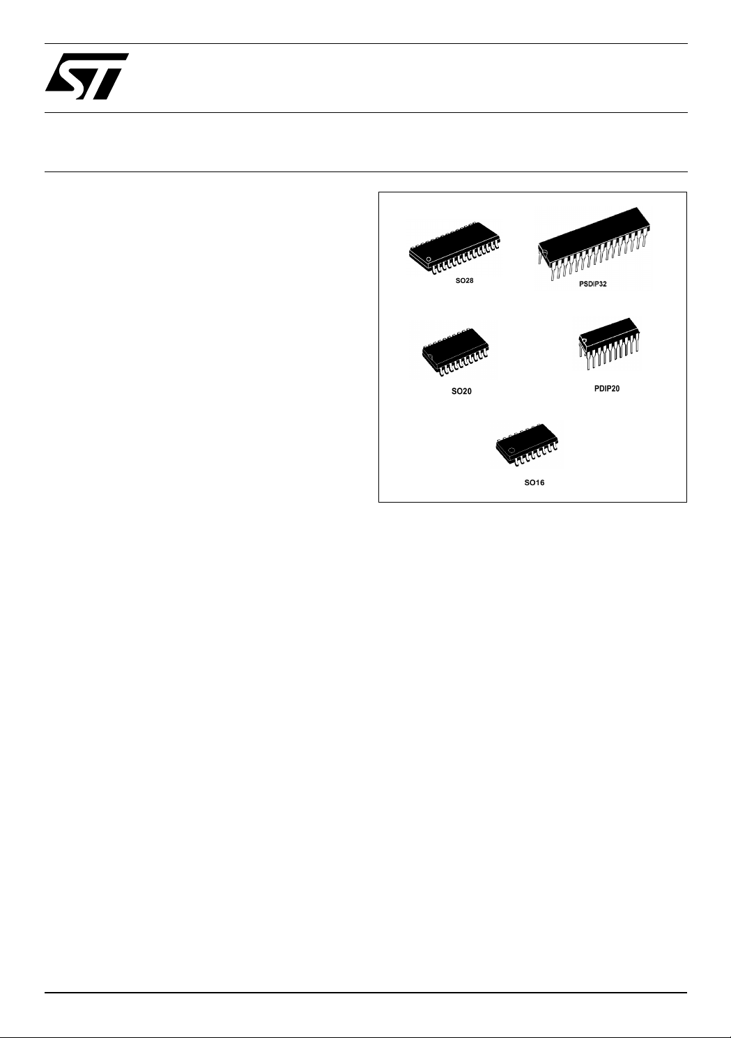
Page 1
®
ST52F510/F513/F514
8-BIT INTELLIGENT CONTROLLER UNIT (ICU)
Two Timer/PWMs, ADC, I2C, SPI, SCI
Memories
■ Up to 8 Kbytes Single Voltage Flash Memory
■ 256 bytes of Register Fi le
■ 256 bytes of RAM
■ Up to 4 Kbytes Data EEPROM
■ In Situ Programming in Flash devices (ISP)
■ Single byte and Page modes and In Application
Programming for writing data in Flash memory
■ Readout protection and flexible write protection
Core
■ Register File based architecture
■ 107 basic instructions
■ Hardware multiplication and division
■ Decision Processor for the implementation of
Fuzzy Logic algorithms
■ Deep System and User Stacks
Clock and Power Supply
■ Up to 24 MHz clock frequency
■ Programmable Oscillator modes:
– 10 MHz Internal Oscillator
– External Clock/ Oscillator
– External RC Oscillator
■ Power-On Reset (POR)
■ Programmable Low Voltage Detector (PLVD)
with 3 configurable thresholds
■ Power Saving features
Interrupts
■ 8 interrupt vectors with one SW Trap
■ Non-Maskable Interrupt (NMI)
■ Two Port Interrupts with up to 16 sources
I/O Ports
■ From 10 up to 22 I/O PINs configurable in pull-
up, push-pull, weak pull-up, open-drain and
high-impedance
■ High current sink/source in all pins
ST52F510/F513/F514
TARGET SPECIFICATION
Peripherals
■ On-chip 10-bit A/D Converter with 8 channel
analog multiplexer and Autocalibration.
■ 2 Programmable 16 bit Timer/PWMs with
internal 16-bit Prescaler featuring:
– PWM output
– Input capture
– Output compare
– Pulse generator mode
■ Watchdog timer
■ Serial Communication Interface (SCI) with
asynchronous protocol (UART).
2
■ I
C Peripheral with master and slave mode
■ 3-wire SPI
Master and Multi Master SPI modes
Development tools
■ High level Software tools
■ ‘C’ Compiler
■ Emulator
■ Low cost Programmer
■ Gang Programmer
Peripheral supporting Single
Rev. 1.18 -June 2003 1/106
This is preliminary information on a new product foreseen to be developed. Details are subject to change without notice.
Page 2

ST52F510/F513/F514
2/106
Page 3

ST52F510/F513/F514
TABLE OF CONTENTS
TABLE OF CONTENTS
1 GENERAL DESCRIPTION. . . . . . . . . . . . . . . . . . . . . . . . . . . . . . . . . . . . . . . . . 7
1.1 Introduction. . . . . . . . . . . . . . . . . . . . . . . . . . . . . . . . . . . . . . . . . . . . . . . . . . . . . . . . . . . . . . . . . . .7
1.2 Functional Description . . . . . . . . . . . . . . . . . . . . . . . . . . . . . . . . . . . . . . . . . . . . . . . . . . . . . . . . . .8
1.2.1 Memory Programming Mode . . . . . . . . . . . . . . . . . . . . . . . . . . . . . . . . . . . . . . . . . . . . . . . . 8
1.2.2 Working Mode. . . . . . . . . . . . . . . . . . . . . . . . . . . . . . . . . . . . . . . . . . . . . . . . . . . . . . . . . . . . 8
1.3 Pin Description . . . . . . . . . . . . . . . . . . . . . . . . . . . . . . . . . . . . . . . . . . . . . . . . . . . . . . . . . . . . . . .16
2 INTERNAL ARCHITECTURE. . . . . . . . . . . . . . . . . . . . . . . . . . . . . . . . . . . . . . 17
2.1 Control Unit and Data Processing Unit . . . . . . . . . . . . . . . . . . . . . . . . . . . . . . . . . . . . . . . . . . . . .17
2.1.1 Program Counter . . . . . . . . . . . . . . . . . . . . . . . . . . . . . . . . . . . . . . . . . . . . . . . . . . . . . . . . 18
2.1.2 Flags. . . . . . . . . . . . . . . . . . . . . . . . . . . . . . . . . . . . . . . . . . . . . . . . . . . . . . . . . . . . . . . . . . 18
2.2 Arithmetic Logic Unit. . . . . . . . . . . . . . . . . . . . . . . . . . . . . . . . . . . . . . . . . . . . . . . . . . . . . . . . . . .19
2.3 Register Description . . . . . . . . . . . . . . . . . . . . . . . . . . . . . . . . . . . . . . . . . . . . . . . . . . . . . . . . . . .20
3 ADDRESSING SPACES. . . . . . . . . . . . . . . . . . . . . . . . . . . . . . . . . . . . . . . . . . 21
3.1 Memory Interface . . . . . . . . . . . . . . . . . . . . . . . . . . . . . . . . . . . . . . . . . . . . . . . . . . . . . . . . . . . . .21
3.2 Register File . . . . . . . . . . . . . . . . . . . . . . . . . . . . . . . . . . . . . . . . . . . . . . . . . . . . . . . . . . . . . . . . .21
3.3 Program/Data Memory . . . . . . . . . . . . . . . . . . . . . . . . . . . . . . . . . . . . . . . . . . . . . . . . . . . . . . . . .21
3.4 System and User Stacks. . . . . . . . . . . . . . . . . . . . . . . . . . . . . . . . . . . . . . . . . . . . . . . . . . . . . . . .23
3.5 Input Registers . . . . . . . . . . . . . . . . . . . . . . . . . . . . . . . . . . . . . . . . . . . . . . . . . . . . . . . . . . . . . . .24
3.6 Output registers . . . . . . . . . . . . . . . . . . . . . . . . . . . . . . . . . . . . . . . . . . . . . . . . . . . . . . . . . . . . . .24
3.7 Configuration Registers & Option Bytes . . . . . . . . . . . . . . . . . . . . . . . . . . . . . . . . . . . . . . . . . . . .25
4 MEMORY PROGRAMMING. . . . . . . . . . . . . . . . . . . . . . . . . . . . . . . . . . . . . . . 31
4.1 Program/Data Memory Organization . . . . . . . . . . . . . . . . . . . . . . . . . . . . . . . . . . . . . . . . . . . . . .31
4.2 Memory Programming . . . . . . . . . . . . . . . . . . . . . . . . . . . . . . . . . . . . . . . . . . . . . . . . . . . . . . . . .32
4.2.1 Programming Mode start . . . . . . . . . . . . . . . . . . . . . . . . . . . . . . . . . . . . . . . . . . . . . . . . . . 32
4.2.2 Fast Programming procedure. . . . . . . . . . . . . . . . . . . . . . . . . . . . . . . . . . . . . . . . . . . . . . . 33
4.2.3 Random data writing. . . . . . . . . . . . . . . . . . . . . . . . . . . . . . . . . . . . . . . . . . . . . . . . . . . . . . 33
4.2.4 Option Bytes Programming. . . . . . . . . . . . . . . . . . . . . . . . . . . . . . . . . . . . . . . . . . . . . . . . . 34
4.3 Memory Verify. . . . . . . . . . . . . . . . . . . . . . . . . . . . . . . . . . . . . . . . . . . . . . . . . . . . . . . . . . . . . . . .35
4.3.1 Fast read procedure . . . . . . . . . . . . . . . . . . . . . . . . . . . . . . . . . . . . . . . . . . . . . . . . . . . . . . 35
4.3.2 Random data reading . . . . . . . . . . . . . . . . . . . . . . . . . . . . . . . . . . . . . . . . . . . . . . . . . . . . . 36
4.4 Memory Lock . . . . . . . . . . . . . . . . . . . . . . . . . . . . . . . . . . . . . . . . . . . . . . . . . . . . . . . . . . . . . . . .36
4.5 ID Code. . . . . . . . . . . . . . . . . . . . . . . . . . . . . . . . . . . . . . . . . . . . . . . . . . . . . . . . . . . . . . . . . . . . .37
4.6 Error cases . . . . . . . . . . . . . . . . . . . . . . . . . . . . . . . . . . . . . . . . . . . . . . . . . . . . . . . . . . . . . . . . . .37
4.7 In-Situ Programming (ISP) . . . . . . . . . . . . . . . . . . . . . . . . . . . . . . . . . . . . . . . . . . . . . . . . . . . . . .38
4.8 In-Application Programming (IAP) . . . . . . . . . . . . . . . . . . . . . . . . . . . . . . . . . . . . . . . . . . . . . . . .38
4.8.1 Single byte write . . . . . . . . . . . . . . . . . . . . . . . . . . . . . . . . . . . . . . . . . . . . . . . . . . . . . . . . . 38
4.8.2 Block write . . . . . . . . . . . . . . . . . . . . . . . . . . . . . . . . . . . . . . . . . . . . . . . . . . . . . . . . . . . . . 38
4.8.3 Memory Corruption Prevention. . . . . . . . . . . . . . . . . . . . . . . . . . . . . . . . . . . . . . . . . . . . . . 38
4.8.4 Option Bytes . . . . . . . . . . . . . . . . . . . . . . . . . . . . . . . . . . . . . . . . . . . . . . . . . . . . . . . . . . . . 39
4.8.5 Input Register . . . . . . . . . . . . . . . . . . . . . . . . . . . . . . . . . . . . . . . . . . . . . . . . . . . . . . . . . . . 39
3/106
Page 4

ST52F510/F513/F514
5 INTERRUPTS . . . . . . . . . . . . . . . . . . . . . . . . . . . . . . . . . . . . . . . . . . . . . . . . . . 40
5.1 Interrupt Processing . . . . . . . . . . . . . . . . . . . . . . . . . . . . . . . . . . . . . . . . . . . . . . . . . . . . . . . . . . .40
5.2 Global Interrupt Request Enabling . . . . . . . . . . . . . . . . . . . . . . . . . . . . . . . . . . . . . . . . . . . . . . . .40
5.3 Interrupt Sources . . . . . . . . . . . . . . . . . . . . . . . . . . . . . . . . . . . . . . . . . . . . . . . . . . . . . . . . . . . . .41
5.4 Interrupt Maskability and Priority Levels . . . . . . . . . . . . . . . . . . . . . . . . . . . . . . . . . . . . . . . . . . . .41
5.5 Interrupt RESET . . . . . . . . . . . . . . . . . . . . . . . . . . . . . . . . . . . . . . . . . . . . . . . . . . . . . . . . . . . . . .41
5.6 Register Description . . . . . . . . . . . . . . . . . . . . . . . . . . . . . . . . . . . . . . . . . . . . . . . . . . . . . . . . . . .42
6 CLOCK, RESET & POWER SAVING MODES . . . . . . . . . . . . . . . . . . . . . . . . 44
6.1 Clock. . . . . . . . . . . . . . . . . . . . . . . . . . . . . . . . . . . . . . . . . . . . . . . . . . . . . . . . . . . . . . . . . . . . . . .44
6.2 Reset. . . . . . . . . . . . . . . . . . . . . . . . . . . . . . . . . . . . . . . . . . . . . . . . . . . . . . . . . . . . . . . . . . . . . . .45
6.2.1 External Reset . . . . . . . . . . . . . . . . . . . . . . . . . . . . . . . . . . . . . . . . . . . . . . . . . . . . . . . . . . 45
6.2.2 Reset Procedures. . . . . . . . . . . . . . . . . . . . . . . . . . . . . . . . . . . . . . . . . . . . . . . . . . . . . . . . 45
6.3 Programmable Low Voltage Detector. . . . . . . . . . . . . . . . . . . . . . . . . . . . . . . . . . . . . . . . . . . . . .46
6.4 Power Saving modes . . . . . . . . . . . . . . . . . . . . . . . . . . . . . . . . . . . . . . . . . . . . . . . . . . . . . . . . . .46
6.4.1 Wait Mode. . . . . . . . . . . . . . . . . . . . . . . . . . . . . . . . . . . . . . . . . . . . . . . . . . . . . . . . . . . . . . 46
6.4.2 Halt Mode . . . . . . . . . . . . . . . . . . . . . . . . . . . . . . . . . . . . . . . . . . . . . . . . . . . . . . . . . . . . . . 46
6.5 Register Description . . . . . . . . . . . . . . . . . . . . . . . . . . . . . . . . . . . . . . . . . . . . . . . . . . . . . . . . . . .48
6.5.1 Configuration Register . . . . . . . . . . . . . . . . . . . . . . . . . . . . . . . . . . . . . . . . . . . . . . . . . . . . 48
6.5.2 Option Bytes . . . . . . . . . . . . . . . . . . . . . . . . . . . . . . . . . . . . . . . . . . . . . . . . . . . . . . . . . . . . 48
7 I/O PORTS . . . . . . . . . . . . . . . . . . . . . . . . . . . . . . . . . . . . . . . . . . . . . . . . . . . . 50
7.1 Introduction. . . . . . . . . . . . . . . . . . . . . . . . . . . . . . . . . . . . . . . . . . . . . . . . . . . . . . . . . . . . . . . . . .50
7.2 Input Mode . . . . . . . . . . . . . . . . . . . . . . . . . . . . . . . . . . . . . . . . . . . . . . . . . . . . . . . . . . . . . . . . . .50
7.3 Output Mode . . . . . . . . . . . . . . . . . . . . . . . . . . . . . . . . . . . . . . . . . . . . . . . . . . . . . . . . . . . . . . . . .50
7.4 Interrupt Mode. . . . . . . . . . . . . . . . . . . . . . . . . . . . . . . . . . . . . . . . . . . . . . . . . . . . . . . . . . . . . . . .50
7.5 Alternate Functions. . . . . . . . . . . . . . . . . . . . . . . . . . . . . . . . . . . . . . . . . . . . . . . . . . . . . . . . . . . .51
7.6 Register Description . . . . . . . . . . . . . . . . . . . . . . . . . . . . . . . . . . . . . . . . . . . . . . . . . . . . . . . . . . .51
7.6.1 Configuration Registers . . . . . . . . . . . . . . . . . . . . . . . . . . . . . . . . . . . . . . . . . . . . . . . . . . . 52
7.6.2 Input Registers . . . . . . . . . . . . . . . . . . . . . . . . . . . . . . . . . . . . . . . . . . . . . . . . . . . . . . . . . . 54
7.6.3 Output Registers. . . . . . . . . . . . . . . . . . . . . . . . . . . . . . . . . . . . . . . . . . . . . . . . . . . . . . . . . 55
8 FUZZY COMPUTATION (DP). . . . . . . . . . . . . . . . . . . . . . . . . . . . . . . . . . . . . . 56
8.1 Fuzzy Inference . . . . . . . . . . . . . . . . . . . . . . . . . . . . . . . . . . . . . . . . . . . . . . . . . . . . . . . . . . . . . .56
8.2 Fuzzyfication Phase . . . . . . . . . . . . . . . . . . . . . . . . . . . . . . . . . . . . . . . . . . . . . . . . . . . . . . . . . . .56
8.3 Inference Phase . . . . . . . . . . . . . . . . . . . . . . . . . . . . . . . . . . . . . . . . . . . . . . . . . . . . . . . . . . . . . .56
8.4 Defuzzyfication . . . . . . . . . . . . . . . . . . . . . . . . . . . . . . . . . . . . . . . . . . . . . . . . . . . . . . . . . . . . . . .57
8.5 Input Membership Function . . . . . . . . . . . . . . . . . . . . . . . . . . . . . . . . . . . . . . . . . . . . . . . . . . . . .57
8.6 Output Singleton. . . . . . . . . . . . . . . . . . . . . . . . . . . . . . . . . . . . . . . . . . . . . . . . . . . . . . . . . . . . . .58
8.7 Fuzzy Rules . . . . . . . . . . . . . . . . . . . . . . . . . . . . . . . . . . . . . . . . . . . . . . . . . . . . . . . . . . . . . . . . .58
9 INSTRUCTION SET . . . . . . . . . . . . . . . . . . . . . . . . . . . . . . . . . . . . . . . . . . . . . 60
9.1 Addressing Modes . . . . . . . . . . . . . . . . . . . . . . . . . . . . . . . . . . . . . . . . . . . . . . . . . . . . . . . . . . . .60
9.2 Instruction Types. . . . . . . . . . . . . . . . . . . . . . . . . . . . . . . . . . . . . . . . . . . . . . . . . . . . . . . . . . . . . .60
10 10-bit A/D CONVERTER . . . . . . . . . . . . . . . . . . . . . . . . . . . . . . . . . . . . . . . . 65
10.1 Introduction . . . . . . . . . . . . . . . . . . . . . . . . . . . . . . . . . . . . . . . . . . . . . . . . . . . . . . . . . . . . . . . . .65
4/106
Page 5

ST52F510/F513/F514
10.2 Functional Description . . . . . . . . . . . . . . . . . . . . . . . . . . . . . . . . . . . . . . . . . . . . . . . . . . . . . . . .66
10.3 Operating Modes . . . . . . . . . . . . . . . . . . . . . . . . . . . . . . . . . . . . . . . . . . . . . . . . . . . . . . . . . . . .66
10.3.1 One Channel Single Mode . . . . . . . . . . . . . . . . . . . . . . . . . . . . . . . . . . . . . . . . . . . . . . . . 66
10.3.2 Multiple Channels Single Mode . . . . . . . . . . . . . . . . . . . . . . . . . . . . . . . . . . . . . . . . . . . . 66
10.3.3 One Channel Continuous Mode . . . . . . . . . . . . . . . . . . . . . . . . . . . . . . . . . . . . . . . . . . . . 66
10.3.4 Multiple Channels Continuous Mode . . . . . . . . . . . . . . . . . . . . . . . . . . . . . . . . . . . . . . . . 67
10.4 Power Down Mode . . . . . . . . . . . . . . . . . . . . . . . . . . . . . . . . . . . . . . . . . . . . . . . . . . . . . . . . . . .67
10.5 A/D Converter Register Description . . . . . . . . . . . . . . . . . . . . . . . . . . . . . . . . . . . . . . . . . . . . . .67
10.5.1 A/D Converter Configuration Registers . . . . . . . . . . . . . . . . . . . . . . . . . . . . . . . . . . . . . . 67
10.5.2 Input Registers . . . . . . . . . . . . . . . . . . . . . . . . . . . . . . . . . . . . . . . . . . . . . . . . . . . . . . . . . 68
11 WATCHDOG TIMER. . . . . . . . . . . . . . . . . . . . . . . . . . . . . . . . . . . . . . . . . . . . 69
11.1 Functional Description . . . . . . . . . . . . . . . . . . . . . . . . . . . . . . . . . . . . . . . . . . . . . . . . . . . . . . . .69
11.2 Register Description . . . . . . . . . . . . . . . . . . . . . . . . . . . . . . . . . . . . . . . . . . . . . . . . . . . . . . . . . .69
12 PWM/TIMERS. . . . . . . . . . . . . . . . . . . . . . . . . . . . . . . . . . . . . . . . . . . . . . . . . 71
12.1 Introduction . . . . . . . . . . . . . . . . . . . . . . . . . . . . . . . . . . . . . . . . . . . . . . . . . . . . . . . . . . . . . . . . .71
12.2 Timer Mode. . . . . . . . . . . . . . . . . . . . . . . . . . . . . . . . . . . . . . . . . . . . . . . . . . . . . . . . . . . . . . . . .71
12.3 PWM Mode . . . . . . . . . . . . . . . . . . . . . . . . . . . . . . . . . . . . . . . . . . . . . . . . . . . . . . . . . . . . . . . . .73
12.3.1 Simultaneous Start . . . . . . . . . . . . . . . . . . . . . . . . . . . . . . . . . . . . . . . . . . . . . . . . . . . . . . 74
12.4 Timer Interrupts. . . . . . . . . . . . . . . . . . . . . . . . . . . . . . . . . . . . . . . . . . . . . . . . . . . . . . . . . . . . . .74
12.5 PWM/Timer 0 Register Description. . . . . . . . . . . . . . . . . . . . . . . . . . . . . . . . . . . . . . . . . . . . . . .74
12.5.1 PWM/Timer 0 Configuration Registers . . . . . . . . . . . . . . . . . . . . . . . . . . . . . . . . . . . . . . . 74
12.5.2 PWM/Timer 0 Input Registers. . . . . . . . . . . . . . . . . . . . . . . . . . . . . . . . . . . . . . . . . . . . . . 75
12.5.3 PWM/Timer 0 Output Registers . . . . . . . . . . . . . . . . . . . . . . . . . . . . . . . . . . . . . . . . . . . . 76
12.6 PWM/Timer 1 Register Description. . . . . . . . . . . . . . . . . . . . . . . . . . . . . . . . . . . . . . . . . . . . . . .77
12.6.1 PWM/Timer 1 Configuration Registers . . . . . . . . . . . . . . . . . . . . . . . . . . . . . . . . . . . . . . . 77
12.6.2 PWM/Timer 1 Input Registers. . . . . . . . . . . . . . . . . . . . . . . . . . . . . . . . . . . . . . . . . . . . . . 78
12.6.3 PWM/Timer 1 Output Registers . . . . . . . . . . . . . . . . . . . . . . . . . . . . . . . . . . . . . . . . . . . . 79
13 SERIAL COMMUNICATION INTERFACE. . . . . . . . . . . . . . . . . . . . . . . . . . . 80
13.1 SCI Receiver block . . . . . . . . . . . . . . . . . . . . . . . . . . . . . . . . . . . . . . . . . . . . . . . . . . . . . . . . . . .80
13.1.1 Recovery Buffer Block . . . . . . . . . . . . . . . . . . . . . . . . . . . . . . . . . . . . . . . . . . . . . . . . . . . 81
13.1.2 SCDR_RX Block. . . . . . . . . . . . . . . . . . . . . . . . . . . . . . . . . . . . . . . . . . . . . . . . . . . . . . . . 81
13.2 SCI Transmitter Block. . . . . . . . . . . . . . . . . . . . . . . . . . . . . . . . . . . . . . . . . . . . . . . . . . . . . . . . .82
13.3 Baud Rate Generator Block . . . . . . . . . . . . . . . . . . . . . . . . . . . . . . . . . . . . . . . . . . . . . . . . . . . .82
13.4 SCI Register Description. . . . . . . . . . . . . . . . . . . . . . . . . . . . . . . . . . . . . . . . . . . . . . . . . . . . . . .84
13.4.1 SCI Configuration Registers . . . . . . . . . . . . . . . . . . . . . . . . . . . . . . . . . . . . . . . . . . . . . . . 84
13.4.2 SCI Input Registers. . . . . . . . . . . . . . . . . . . . . . . . . . . . . . . . . . . . . . . . . . . . . . . . . . . . . . 85
13.4.3 SCI Output Register . . . . . . . . . . . . . . . . . . . . . . . . . . . . . . . . . . . . . . . . . . . . . . . . . . . . . 85
14 I2C BUS INTERFACE (I2C) . . . . . . . . . . . . . . . . . . . . . . . . . . . . . . . . . . . . . . 86
14.1 Introduction . . . . . . . . . . . . . . . . . . . . . . . . . . . . . . . . . . . . . . . . . . . . . . . . . . . . . . . . . . . . . . . . .86
14.2 Main Features. . . . . . . . . . . . . . . . . . . . . . . . . . . . . . . . . . . . . . . . . . . . . . . . . . . . . . . . . . . . . . .86
14.3 General Description . . . . . . . . . . . . . . . . . . . . . . . . . . . . . . . . . . . . . . . . . . . . . . . . . . . . . . . . . .86
5/106
Page 6

ST52F510/F513/F514
14.3.1 Mode Selection . . . . . . . . . . . . . . . . . . . . . . . . . . . . . . . . . . . . . . . . . . . . . . . . . . . . . . . . . 86
14.3.2 Communication Flow . . . . . . . . . . . . . . . . . . . . . . . . . . . . . . . . . . . . . . . . . . . . . . . . . . . . 86
14.3.3 SDA/SCL Line Control . . . . . . . . . . . . . . . . . . . . . . . . . . . . . . . . . . . . . . . . . . . . . . . . . . . 87
14.4 Functional Description . . . . . . . . . . . . . . . . . . . . . . . . . . . . . . . . . . . . . . . . . . . . . . . . . . . . . . . .87
14.4.1 Slave Mode. . . . . . . . . . . . . . . . . . . . . . . . . . . . . . . . . . . . . . . . . . . . . . . . . . . . . . . . . . . . 87
14.4.2 Master Mode. . . . . . . . . . . . . . . . . . . . . . . . . . . . . . . . . . . . . . . . . . . . . . . . . . . . . . . . . . . 88
14.5 Register Description . . . . . . . . . . . . . . . . . . . . . . . . . . . . . . . . . . . . . . . . . . . . . . . . . . . . . . . . . .92
14.5.1 I2C Interface Configuration Registers. . . . . . . . . . . . . . . . . . . . . . . . . . . . . . . . . . . . . . . . 92
14.5.2 I2C Interface Input Registers . . . . . . . . . . . . . . . . . . . . . . . . . . . . . . . . . . . . . . . . . . . . . . 93
14.5.3 I2C Interface Output Registers . . . . . . . . . . . . . . . . . . . . . . . . . . . . . . . . . . . . . . . . . . . . . 95
15 SERIAL PERIPHERAL INTERFACE (SPI) . . . . . . . . . . . . . . . . . . . . . . . . . . 96
15.1 Introduction . . . . . . . . . . . . . . . . . . . . . . . . . . . . . . . . . . . . . . . . . . . . . . . . . . . . . . . . . . . . . . . . .96
15.2 Main Features. . . . . . . . . . . . . . . . . . . . . . . . . . . . . . . . . . . . . . . . . . . . . . . . . . . . . . . . . . . . . . .96
15.3 General description. . . . . . . . . . . . . . . . . . . . . . . . . . . . . . . . . . . . . . . . . . . . . . . . . . . . . . . . . . .96
15.4 Functional Description . . . . . . . . . . . . . . . . . . . . . . . . . . . . . . . . . . . . . . . . . . . . . . . . . . . . . . . .96
15.4.1 Master Configuration . . . . . . . . . . . . . . . . . . . . . . . . . . . . . . . . . . . . . . . . . . . . . . . . . . . . 96
15.4.2 Slave Configuration . . . . . . . . . . . . . . . . . . . . . . . . . . . . . . . . . . . . . . . . . . . . . . . . . . . . . 98
15.4.3 Data Transfer Format . . . . . . . . . . . . . . . . . . . . . . . . . . . . . . . . . . . . . . . . . . . . . . . . . . . . 98
15.4.4 Write Collision Error . . . . . . . . . . . . . . . . . . . . . . . . . . . . . . . . . . . . . . . . . . . . . . . . . . . . . 98
15.4.5 Master Mode Fault . . . . . . . . . . . . . . . . . . . . . . . . . . . . . . . . . . . . . . . . . . . . . . . . . . . . . . 99
15.4.6 Overrun Condition. . . . . . . . . . . . . . . . . . . . . . . . . . . . . . . . . . . . . . . . . . . . . . . . . . . . . . 101
15.4.7 Single Master and Multimaster Configurations. . . . . . . . . . . . . . . . . . . . . . . . . . . . . . . . 101
15.4.8 Interrupts. . . . . . . . . . . . . . . . . . . . . . . . . . . . . . . . . . . . . . . . . . . . . . . . . . . . . . . . . . . . . 102
15.5 SPI Register Description. . . . . . . . . . . . . . . . . . . . . . . . . . . . . . . . . . . . . . . . . . . . . . . . . . . . . .103
15.5.1 SPI Configuration Registers . . . . . . . . . . . . . . . . . . . . . . . . . . . . . . . . . . . . . . . . . . . . . . 103
15.5.2 SPI Input Register. . . . . . . . . . . . . . . . . . . . . . . . . . . . . . . . . . . . . . . . . . . . . . . . . . . . . . 104
15.5.3 SPI Output Register . . . . . . . . . . . . . . . . . . . . . . . . . . . . . . . . . . . . . . . . . . . . . . . . . . . . 105
6/106
Page 7

ST52F510/F513/F514
1 GENERAL DESCRIPTION
1.1 Introduction
ST52F510/F513/F514 are devices of ST FIVE
family of 8-bit Intelligent Controller Units (ICU),
which can perform, both boolean and Fuzzy
algorithms in an efficient manner, in order to reach
the best performances that the two methodologies
allow.
Produced by STMicroelectronics using the reliable
high performance CMOS process for Single
Voltage Flash versions, ST52F510/F513/F514
include integrated on-chip peripherals that allow
maximization of system re liability, and decreased
system costs in orde r to minimize the number of
external components.
The flexible I/O co nfiguration of ST52F510/F513/
F514 allow one to interf ace with a wide range of
external devices (for example D/A converters or
power control devices), and to c ommunicate with
the most common serial standards.
ST52F510/F513/F514 pins are configurable. The
user can set input or output signals on each single
pin in 8 different modes, reducing the need for
external components in orde r to supply a suitable
interface with the port pins.
A hardware multiplier an d divider, together wit h a
wide instruction set, allow the implementation of
complex functions by using a single instruction.
Therefore, program memory utilization and
computational speed is optimized.
Fuzzy Logic dedicated structures in ST52F510/
F513/F514 ICU’s can be exploited to model
complex system with high accuracy in a useful and
simple manner.
Fuzzy Expert Systems for overall system
management and Fuzzy Real time Controls can be
designed to increase per formance at competitive
costs.
The linguistic approach characterizing Fuzzy Logic
is based on a set of IF-THEN rules, which describe
the control behavior and on Membership Functions
associated with input and output variables.
Up to 340 Membership Fun ctions, with triangular
and trapezoidal shapes, or singleton values are
available to describe fuzzy variables.
The Timer/PWM periph eral all ows o ne to m anage
power devices and timing signals, by implementing
different operating modes and high frequency
PWM (Pulse Width Modulation) controls. Input
Capture and Output Compare functions are
available on the Timers.
The Timer has a 16-bit programmable internal
Prescaler and a 16-bit Counter, which can use
internal or external START/STOP signals and
clock.
An internal programmable WATCHDOG is
available to avoid loop errors and reset the ICU.
ST52F510/F513/F514 includes a 10-bit, selfcalibrating, Analog to Digital Converter with an 8 analog channel Multiplexer. Single/Multiple
channels and Single/Sequence conversion modes
are supported. External reference can be supplied
to obtain more stability and precision in the
conversion.
ST52F510/F513/F514 supply differ ent per ipheral s
to implement the most common serial
communication protocols. SCI allows the
performance of serial asynchronous
communication (UART). I
allow the implementation of synchronous serial
protocols. I
2
C peripherals can work both in master
2
C and SPI peripherals
and slave mode. SPI imple ments S ingle and Mul ti
Master modes using 3-wire.
Up to 8 interrupt vectors are available, which allow
synchronization with peripherals and external
devices. Non-Maskable Int errupt and S/W TRAP
are available. All interrupts have configurable
priority levels and are maskable excluding the
Non-Maskable Interr upt, which has fixed top level
priority. Two versatile Por t Interru pts are avail able
for synchronization with external sources.
The ST52F510/F513/F514 also include an on-chip
Power-on-Reset (POR), which provides an internal
chip reset during power up situation and a
Programmable Low Voltage Detector (PLVD),
which causes the ICU to reset if the voltage source
V
dips below a thresho ld. Three progr ammable
DD
thresholds are available, allowing to work with
different supply voltages (from 2.7 to 5.5 V).
In order to optimize energy consumption, two
different power savin g modes are available: Wait
mode and Halt mode.
Internal Oscillator at 10 MHz ± 1% is available.
External clock, quartz oscillator or RC oscillator are
also applicable. The device alw ays starts with the
Internal Oscillator, then it reads an Option Byte
where the clock mode to be used is programmed.
Program Memory addressing capability addresses
up to 8 Kbytes of memory location to store both
program instructions and data.
Memory can be locked by the user in order to
prevent external undesired operations.
Operations may be performed on data stored in
RAM, allowing direct combination of new inputs
and feedback data. All RAM bytes are used like
Register File.
An additional RAM bench is added to the Program
Memory addressing space in order to allow the
management of the S y ste m/User Sta ck s an d u se r
data storage.
7/106
Page 8

ST52F510/F513/F514
ST52F510/F513/F514 supply the system stack
and the user stack located in the addit ional RAM
bench. The user stack can be located anywhere in
the additional RAM by writing the top address in
the configuration registers, in order to avoid
overlap with other data.
Single Voltage Flash allo ws the use r to reprogram
the devices on-board by means of the In Situ
Programming (ISP) feature. It is possible to store in
safe way up to 4K of data in the available EEPROM
memory benches. Perma nent data, both in Flash
and EEPROM can be man aged by means of the
In-Application-Programming (IAP) feature. Single
byte and Page write modes are supported. Flexible
write protection, of permanent data or program
instructions, is also available.
The Instruction Set composed of up to 107
instructions allows code compression and high
speed in the program implementation.
A powerful development environment consisting of
a board and software tools allows an easy
configuration and use of ST52F510/F513 /F514 .
The Visual FIVE software tool allows the
development and debugging of projects via a userfriendly graphical interface and optimization of
generated microcode.
Third-party Hardwa re Emulato rs and ‘C ’ Compiler
are available to speed-up the application
implementation and time-to-market.
1.2 Functional Description
ST52F510/F513/F514 ICU’s can work in two
modes according to the Vpp signal levels:
■ Memory Programming Mode
■ Working Mode
During Working Mode Vpp must be tied to Vss. To
enter the Memory Programming Mode, the Vpp pin
must be tied to Vdd.
A RESET signal must be appli ed to the device to
switch from one mode to the other.
1.2.1 Memory Programming Mode.
The ST52F510/F513/F514 memory is loaded in
the Memory Programming Mode. All instructions
and data are written inside the memory during this
phase.
The Option Bytes are l oaded during t his p hase b y
using the programming tools. The Option Bytes
can only be loaded in this phase and cannot be
modified run-time.
Data and commands are trans mitted by using the
2
I
C protocol, implemented using the internal I2C
peripheral. The In-Situ Programming protocol
(ISP) uses the following pins:
■ SDA and SCL for transmission
■ Vpp for entering in the mode
■ RESET for starting the protocol in a stable status
■ Vdd and Vss for the power supply.
The Internal clock is used in this phase.
1.2.2 Working Mode.
The processor starts the wor king phase following
the instructions, which have been previously
loaded in the first locations of the memory. The first
instruction must be a jump to the first program
instruction, skipping the data (interrupt vectors,
Membership Functions, user data) stored in the
first memory page.
ST52F510/F513/F514’s internal structure includes
two computational blocks, the CONTROL UNIT
(CU) and the DATA PROCESSING UNI T (DPU),
which performs boolean functions. The DECISION
PROCESSOR (DP) block cooperates with these
blocks to perform Fuzzy algorithms.
The DP can manage up to 340 different
Membership Function s for the antecedent part of
fuzzy rules. The conseq uent terms of the rules are
“crisp” values (real numbers). The maximum
number of rules that can be defi ned is limited by
the dimensions of the standard algorithm
implemented.
The Program/Data Memory is shared between
Fuzzy and standard algorithms. Within this
memory, the user d ata can be s tored both in n on
volatile memory as well as in the RAM locations.
The Control Unit (CU) reads informati on and the
status of the peripherals.
Arithmetic calculus can be performed on these
values by using t he inte rnal CU and Register File,
which supports all c omputations. The peripheral
inputs can be Fuzzy and/or arithmetic output
values contained in the Register File or Pr ogram/
Data Memory.
8/106
Page 9
ST52F510/F513/F514
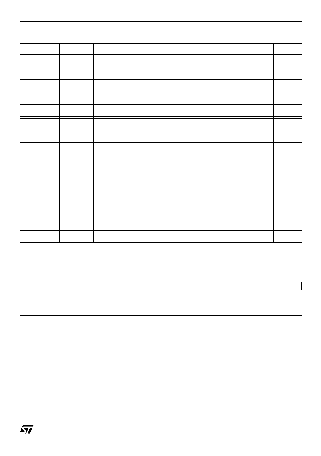
Table 1.1 ST52F510/F513/F514 Devices Summary
Device NVM RF RAM EEPROM Timers ADC Comms I/O Package
ST52F510YmM6 4/8 K FLASH 256 256 - 2X16-bit
ST52F510FmM6 4/8 K FLASH 256 256 - 2X16-bit
ST52F510FmB6 4/8 K FLASH 256 256 - 2X16-bit
ST52F510GmM6 4/8 K FLASH 256 256
ST52F510GmB6 4/8 K FLASH 256 256 - 2X16-bit
ST52F513YmM6 4/8 K FLASH 256 256 256 2X16-bit
ST52F513FmM6 4/8 K FLASH 256 256 256 2X16-bit
ST52F513FmB6 4/8 K FLASH 256 256 256 2X16-bit
ST52F513GmM6 4/8 K FLASH 256 256 256 2X16-bit
ST52F513GmB6 4/8 K FLASH 256 256 256 2X16-bit
ST52F514YmM6 4 K FLASH 256 256 1024 / 4096 2X16-bit
ST52F514FmM6 4 K FLASH 256 256 1024 / 4096 2X16-bit
ST52F514FmB6 4 K FLASH 256 256 1024 / 4096 2X16-bit
ST52F514GmM6 4 K FLASH 256 256 1024 / 4096 2X16-bit
ST52F514GmB6 4 K FLASH 256 256 1024 / 4096 2X16-bit
-
2X16-bit
10-bit
2 Ch
10-bit
6 Ch
10-bit
6 Ch
10-bit
8 Ch
10-bit
8 Ch
10-bit
2 Ch
10-bit
6 Ch
10-bit
6 Ch
10-bit
8 Ch
10-bit
8 Ch
10-bit
2 Ch
10-bit
6 Ch
10-bit
6 Ch
10-bit
8 Ch
10-bit
8 Ch
SCI I
SCI I
SCI I
SCI I
SCI I
SCI I
SCI I
SCI I
SCI I
SCI I
SCI I
SCI I
SCI I
SCI I
SCI I
2
C SPI
2
C SPI
2
C SPI
2
C SPI
2
C SPI
2
C SPI
2
2
2
2
2
2
2
2
2
C
C
C
C
C
C
C
C
C
10 So 16
14 So 20
14 Dip 20
22 So 28
22 SDip 32
10 So 16
14 So 20
14 Dip 20
22 So 28
22 SDip 32
10 So 16
14 So 20
14 Dip 20
22 So 28
22 SDip 32
COMMON FEATURES ST52F510/F513 /F5 14
Watchdog Yes
Other Features NMI, PLVD, POR
Temperature Range From -40° to +85
Operating Supply 2.7 - 5.5 V
CPU Frequency from 1 to 24 MHz.
Legend:
Sales code: ST52tnnncmpy
Memory type (t): F=FLASH
Subfamily (nnn): 510, 513, 514
Pin Count (c): Y=16 pins, F=20 pins, G=28 pins, K=32/34 pins
Memory Size (m):
Packages (p): B=PDIP, M=PSO, T=TQFP
Temperature (y): 0=+25, 1=0 +70, 3=-40 +125, 5=-10 +85, 6=-40 +85, 7=-40 +105
2=4 Kb, 3=8 Kb Flash (ST52F510 & ST52F513)
1=1024, 3=4096 EEPROM (only ST52F514)
°
9/106
Page 10
ST52F510/F513/F514
Figure 1.1 ST52F510/F513/F514 Block Diagram
MEMORY
FLASH
ISP/IAP
DATA RAM
256 bytes
DATA
EEPROM
MEMORY
INTERFACE
I2C
PA7:0
PORT A
TIMER/PWM 0
TIMER/PWM 1
CORE
ALU &
DPU
DECISION
PROCESSOR
CONTROL
UNIT
Register File
256 bytes
Input
registers
ADC
PORT B
SPI
PORT C
SCI
PC FLAGS
WATCHDOG
POWER SUPPLY
& PLVD
VDD VPP VSS OSCIN OSCOUT RESET
OSCILLATOR
POWER ON
RESET
PB7:0
PC5:0
10/106
Page 11
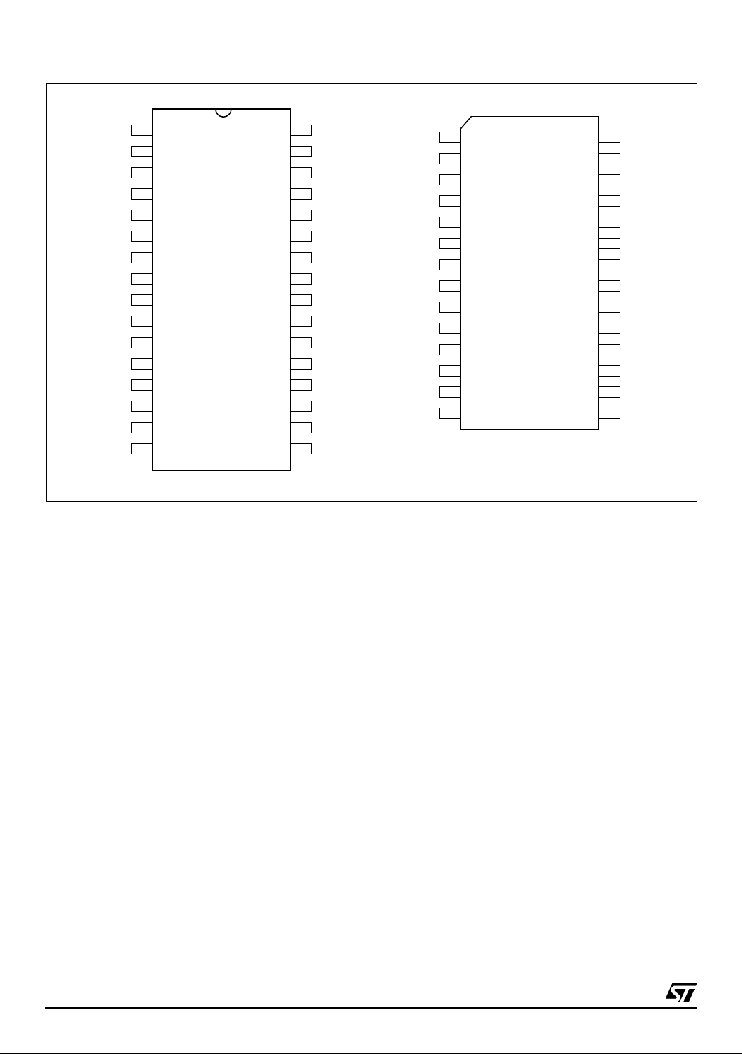
Figure 1.2 ST52F510/F513/F514 SO20/DIP20 Pin Configuration
ST52F510/F513/F514
Vdd
OscOut
OscIn
Vpp
PB0/VREF/AIN0
PB1/AIN1
PB2/AIN2
PB3/AIN3
PB4/AIN4
PB5/AIN5
1
2
3
4
5
6
7
8
9
10
SO20 DIP20
20
19
18
17
16
15
14
13
12
11
Vss
RESET
PA0/SCL
PA1/SDA
PA2/T1OUT
PA3/RX
PA4/TSTRT
PA5/TCLK/TX
PA6/T0OUT
PA7/INT
OscOut
PB0/VREF/AIN0
PB1/AIN1
PB2/AIN2
PB3/AIN3
PB4/AIN4
PB5/AIN5
Figure 1.3 ST52F510/F513/F514 SO16 Pin Configuration
Vdd
OscIn
Vpp
1
2
3
4
5
6
7
8
9
10
20
19
18
17
16
15
14
13
12
11
Vss
RESET
PA0/SCL
PA1/SDA
PA2/T1OUT
PA3/RX
PA4/TSTRT
PA5/TCLK/TX
PA6/T0OUT
PA7/INT
Vdd
OscOut
OscIn
Vpp
PB0/VREF/AIN0
PB1/AIN1
PA7/INT
PA6/T0OUT
1
2
3
4
5
6
7
8
SO16
16
15
14
13
12
11
10
9
Vss
RESET
PA0/SCL
PA1/SDA
PA2/T1OUT
PA3/RX
PA4/TSTRT
PA5/TCLK/TX
11/106
Page 12
ST52F510/F513/F514
Figure 1.4 ST52F510/F513/F514 SDIP32/DIP28 Pin Configuration
Vdd
VddIO
OscOut
OscIn
Vpp
PB0/VREF/AIN0
PB1/AIN1
PB2/AIN2
PB3/AIN3
PB4/AIN4
PB5/AIN5
PB6/AIN6
PB7AIN7
PC0/SCK
PC1/MOSI
N.C.
1
2
3
4
5
6
7
8
9
10
11
12
13
14
15
16
SDIP32
32
31
30
29
28
27
26
25
24
23
22
21
20
19
18
17
Vss
VssIO
RESET
PA0/SCL
PA1/SDA
PA2/T1OUT
PA3/RX
PA4/TSTRT
PA5/TCLK/TX
PA6/T0OUT
PA7/INT
PC5/TRES
PC4/TX
PC3/SS
PC2MISO
N.C.
Vdd
OscOut
OscIn
Vpp
PB0/VREF/AIN0
PB1/AIN1
PB2/AIN2
PB3/AIN3
PB4/AIN4
PB5/AIN5
PB6/AIN6
PB7/AIN7
PC0/SCK
PC1/MOSI
1
2
3
4
5
6
7
8
9
10
11
12
13
14
SO28
28
27
26
25
24
23
22
21
20
19
18
17
16
15
Vss
RESET
PA0/SCL
PA1/SDA
PA2/T1OUT
PA3/RX
PA4/TSTRT
PA5/TCLK/TX
PA6/T0OUT
PA7/INT
PC5/TRES
PC4/TX
PC3/SS
PC2/MISO
12/106
Page 13

ST52F510/F513/F514
Table 1.2 ST52F510/F513/F514 SDIP32 Pin List
SDIP32 NAME Programming Phase Working Phase
1 Vdd Digital Power Supply Digital Power Supply
2 VddIO Digital Power Supply Digital I/O Ports Power Supply
3 OSCOUT Oscillator Output
4 OSCIN Oscillator Input
5 Vpp Programming Mode Selector Programming Mode Selector
6 PB0/VREF/AIN0 Digital I/O, A/D Voltage Reference, Analog Input
7 PB1/AIN1 Digital I/O, Analog Input
8 PB2/AIN2 Digital I/O, Analog Input
9 PB3/AIN3 Digital I/O, Analog Input
10 PB4/AIN4 Digital I/O, Analog Input
11 PB5/AIN5 Digital I/O, Analog Input
12 PB6/AIN6 Digital I/O, Analog Input
13 PB7/AIN7 Digital I/O, Analog Input
14 PC0/SCK Digital I/O, SPI Serial Clock
15 PC1/MOSI Digital I/O, SPI Master out Slave in
16 N.C Not Connected
17 N.C Not Connected
18 PC2/MISO Digital I/O, SPI Master in Slave out
19 PC3/SS Digital I/O, SPI Slave Select
20 PC4/TX Digital I/O, SCI Transmission
21 PC5/TRES Digital I/O, Timer/PWM 0 Reset
22 PA7/INT Digital I/O, Non Maskable Interrupt
23 PA6/T0OUT Digital I/O, Timer/PWM 0 output
24 PA5/TCLK/TX Digital I/O, Timer/PWM 0 clock
25 PA4/TSTRT Digital I/O, Timer/PWM 0 start/stop
26 PA3/RX Digital I/O, SCI Reception
27 PA2/T1OUT Digital I/O, Timer/PWM 1 output
28 PA1/SDA Serial Data I/O
29 PA0/SCL Serial Clock
30 RESET General Reset General Reset
Digital I/O, I
Digital I/O, I
2
C Serial Data I/O
2
C Serial Clock
31 VssIO Digital Ground Digital I/O Ports Ground
32 Vss Digital Ground Digital Ground
13/106
Page 14

ST52F510/F513/F514
Table 1.3 ST52F510/F513/F514 SO28 Pin List
SO28 NAME Programming Phase Working Phase
1 Vdd Digital Power Supply Digital Power Supply
2 OSCOUT Oscillator Output
3 OSCIN Oscillator Input
4 Vpp Programming Mode Selector Programming Mode Selector
5 PB0/VREF/AIN0 Digital I/O, A/D Voltage Reference, Analog Input
6 PB1/AIN1 Digital I/O, Analog Input
7 PB2/AIN2 Digital I/O, Analog Input
8 PB3/AIN3 Digital I/O, Analog Input
9 PB4/AIN4 Digital I/O, Analog Input
10 PB5/AIN5 Digital I/O, Analog Input
11 PB6/AIN6 Digital I/O, Analog Input
12 PB7/AIN7 Digital I/O, Analog Input
13 PC0/SCK Digital I/O, SPI Serial Clock
14 PC1/MOSI Digital I/O, SPI Master out Slave in
15 PC2/MISO Digital I/O, SPI Master in Slave out
16 PC3/SS Digital I/O, SPI Slave Select
17 PC4/TX Digital I/O, SCI Transmission
18 PC5/TRES Digital I/O, Timer/PWM 0 Reset
19 PA7/INT Digital I/O, Non Maskable Interrupt
20 PA6/T0OUT Digital I/O, Timer/PWM 0 output
21 PA5/TCLK/TX Digital I/O, Timer/PWM 0 clock
22 PA4/TSTRT Digital I/O, Timer/PWM 0 start/stop
23 PA3/RX Digital I/O, SCI Reception
24 PA2/T1OUT Digital I/O, Timer/PWM 1 output
25 PA1/SDA Serial Data I/O
26 PA0/SCL Serial Clock
27 RESET General Reset General Reset
28 Vss Digital Ground Digital Ground
Digital I/O, I
Digital I/O, I
2
C Serial Data I/O
2
C Serial Clock
14/106
Page 15

Table 1.4 ST52F510/F513/F514 SO20/DIP20/SO16 Pin List
ST52F510/F513/F514
SO20
DIP20
SO16 NAME Programming Phase Working Phase
1 1 Vdd Digital Power Supply Digital Power Supply
2 2 OSCOUT Oscillator Output
3 3 OSCIN Oscillator Input
4 4 Vpp Programming Mode Selector Programming Mode Selector
5 5 PB0/VREF/AIN0 Digital I/O, A/D Voltage Reference, Analog Input
6 6 PB1/AIN1 Digital I/O, Analog Input
7 - PB2/AIN2 Digital I/O, Analog Input
8 - PB3/AIN3 Digital I/O, Analog Input
9 - PB4/AIN4 Digital I/O, Analog Input
10 - PB5/AIN5 Digital I/O, Analog Input
11 7 PA7/INT Digital I/O, Non Maskable Interrupt
12 8 PA6/T0OUT Digital I/O, Timer/PWM 0 output
13 9 PA5/TCLK/TX Digital I/O, Timer/PWM 0 clock, SCI transmission
14 10 PA4/TSTRT Digital I/O, Timer/PWM 0 start/stop
15 11 PA3/RX Digital I/O , SCI Re ce ptio n
16 12 PA2/T1OUT Digital I/O, Timer/PWM 1 output
17 13 PA1/SDA Serial Data I/O
18 14 PA0/SCL Serial Clock
19 15 RESET General Reset General Reset
20 16 Vss Digital Ground Digital Ground
Digital I/O, I
Digital I/O, I
2
C Serial Data I/O
2
C Serial Clock
15/106
Page 16

ST52F510/F513/F514
1.3 Pin Description
ST52F510/F513/F514 pins can be set in digital
input mode, digital output mo de, i nterr upt mode or
in Alternate Functions. Pin configuration is
achieved by mean s of the config uration registe rs.
The functions of the ST52F510/F513/F514 pins
are described below:
V
Main Power Supply Voltage.
DD.
I/O Ports Power Supply Voltage. It is
V
DDIO.
reccomended to connect this pin with a supply
voltage de-coupled with V
in order to improve
DD
the immunity from the n oise generated by th e I/O
switching.
V
. Digital circuit Ground.
SS
. I/O Ports Ground. See V
V
SSIO
DDIO
VPP. Programming/Working mode selector. During
the Programming p hase V
In Working phase V
PP
must be set to VDD.
PP
must be equal to VSS.
OSCin and OSCout. These pins are internally
connected to the on-chip oscillator circuit. A quartz
crystal or a ceramic resonator can be connected
between these two pins in order to allow correct
use of ST52F510/F513/F514 with various stability/
cost trade-offs. An external clock signal can be
applied to OSCin: in this case OSCout must be
grounded. To reduce costs, an RC cir cuit can be
applied to the OSCin pi n to establish the internal
clock frequency, instead of the quartz. Without any
connection, the device can work with its internal
clock generator (10 MHz)
PA0-PA7, PB0-PB7,PC0-PC5. These lines are
organized as I/O ports. Each pin can be configured
as an input, output (with pull- up, pus h-pull, weakpull-up, open-drain, high-impedance), or as an
interrupt source.
VREF, AIN0-AIN7. These pins are used to input
the analog signals into the A/D Converter. An
analog multiplexer is available to switch these
inputs to the A/D Converter. The pin VREF is used
to input an external A/D Reference Voltage.
T0OUT, T1OUT. These pins output the signals
generated by the PWM/Timer 0 and PWM/Timer 1
peripheral.
TRES, TSTRT, TCLK . These pins are related to
the PWM/Timer 0 peripheral and are used for Input
Capture and event counting. The TRES pin is used
to set/reset the Timer; the TSTRT pin is used to
start/stop the counter. The Timer can be driven by
the internal clock or by an external signal
connected to the TCLK pin.
INT. This pin is used as input for the Non-Maskable
(top level) interrupt. The interrupt signal is detected
only if the pin is configured in Alternate Function.
SCL, SDA. These pin are used respectively as
Serial Clock and Serial Data I/O in I
2
C peripheral
protocol. They are used also in Programming
Mode to receive and transmit data.
TX, RX. Serial data output of SCI Transmitter block
(TX) and Serial data input of the SCI Receiver
block (RX).
RESET. This signal is used to reset the ST52F510/
F513/F514 and re-initialize the registers and
control signals. It is also used when switching from
the Programming Mode to Working Mode and vice
versa.
16/106
SCK, MISO, MOSI, SS. These pins are used by
the Serial Peripheral Interface (SPI) peripheral.
SCK is the serial clock line. MISO (Master In Slave
Out) and MOSI (Master Out Slave In) are the serial
data lines, which work in input or in output
depending on if the devic e is working in slave or
master mode. The SS pin allows the selection of
the device master/slave mode.
Page 17
ST52F510/F513/F514
Control
Signals
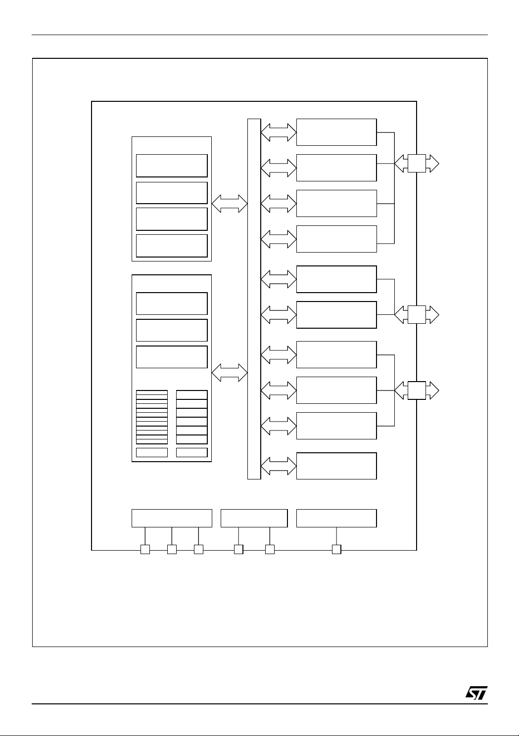
2 INTERNAL ARCHITECTURE
ST52F510/F513/F514’s architecture is Register
File based and is composed of the following blocks
and peripherals:
■ Control Unit (CU)
■ Data Processing Unit (DPU)
■ Decision Processor (DP)
■ ALU
■ Memory Interface
■ up to 256 bytes Register File
■ Program/Data Memory
■ Data EEPROM
■ Interrupts Controller
■ Clock Oscillator
■ PLVD and POR
■ Digital I/O ports
■ Analog Multiplexer and A/D Converter
■ Timer/PWMs
2
■ I
C
■ SPI
■ SCI
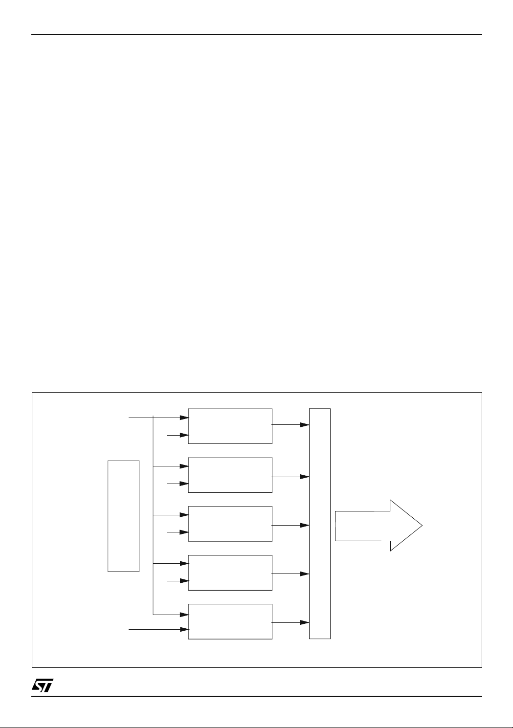
Figure 2.1 CU Block Diagram
2.1 Control Unit and Data Processing Unit
The Control Unit (CU) decodes the instructions
stored in the Program Mem ory and gene rates the
appropriate control s ignals. The main parts of the
CU are illustrated in Figure 2.1.
The five different parts of the CU manage Loading,
Logic/Arithmetic, Jump, Control and the Fuzzy
instruction set.
The block called “ Collector” manages the sig nals
deriving from the different parts of the CU. The
collector defines the signals for the Data
Processing Unit (DPU) and Decision Processor
(DP), as well as for th e different peripherals of the
ICU.
The block called “Arbiter” manages the different
parts of the CU, so that only one part of the system
is activated during working mode.
The CU structure is extremely flexible and was
designed with the purp ose of easily adapting the
core of the microcontroller to market need s. New
instruction sets or new pe ripherals can easil y be
included without changing the structure of the
microcontroller, maintaining code compatibility.
A set of 107 different instructions is available. Each
instruction requires a number of clock pulses to be
performed that depe nds on the complexity of the
instruction it self. The clock pulses t o execute the
instructions are driv en dir ec tly by the ma sterclock,
which has the same frequency of the oscillator
signal supplied.
MicroCode
A
R
B
I
T
E
R
Clock Master
Loading
Instruction Set
Logic Arithmetic
Instruction Set
Jump
Instruction Set
Control
Instruction Set
Decision Processor
Instruction Set
C
O
L
L
E
C
T
O
R
17/106
Page 18

ST52F510/F513/F514
Figure 2.2 Data Processing Unit (DPU)
Interrupts Unit
Program Memory
Input Registers
Peripherals
REGISTER FILE
ADDRESS
PROGRAM COUNTER
REGISTER
FILE
256 Bytes
ACCUMULATOR
FLAGS REG.
DECISION
PROCESSOR
REGISTERS
ALU
Memory Address
Control Unit
Peripherals
The DPU receives, stores and sends the
instructions deriving from the Program/Data
Memory, Register File or from the peripherals. It is
controlled by the CU on the basis of the dec oded
instruction. The Fuzzy registers store the partial
results of the f uz zy c om puta tion. The accumul ator
register is used by the ALU and i s not accessible
directly: the instructions used by the ALU can
address all the Register File locations as
operands, allowing a more compact code and a
faster execution.
The following addressing modes are available:
inherent, immediate, direct, indirect, bit direct.
2.1.1 Program Counter.
The Program Counter (PC) is a 16-bit register that
contains the addre ss of the next memory location
to be processed by the core. This memory location
may be both an instruction or data address.
The Program Counter’s 16-bit length allows the
direct addressing of a maximum of 64 Kbytes in the
Program/Data Memory space.
18/106
The PC can be changed in the following ways:
■ JP (Jump) PC = Jump Address
■ Interrupt PC = Interrupt Vector
■ RETI PC = Pop (stack)
■ RET PC = Pop (stack)
■ CALL PC = Subroutines address
■ Reset PC = Reset Vector
■ Normal Instruction PC = PC + 1
2.1.2 Flags.
The ST FIVE core includes differen t sets of flags
that correspond to 2 different modes: normal mode
and interrupt mode. Each set of fla gs consist of a
CARRY flag (C), ZERO flag (Z) and SIGN flag (S).
Each set is stacked: one set of flags is used during
normal operation and oth er sets are used during
each level of interrupt. Formally, the user has to
manage only one set of flags: C, Z and S since the
flag stack operation is performed automatically.
Page 19

ST52F510/F513/F514
Each interrupt leve l ha s i t s own set of flags, which
is saved in the Flag Stack during interrupt
servicing. These flags are restored from the Flag
Stack automatically when a RETI instruction is
executed.
If the ICU was in normal mode before an interrupt,
after the RETI instruction is executed, the normal
flags are restored.
Note: A subroutine CALL is a normal mode
execution. For this reason a RET instruction,
consequent to a CALL instruction, doesn’t affect
the normal mode set of flags.
Flags are not cleared during context switching and
remain in the state they were in at the exit of the
last interrupt routine switching.
The Carry flag is set when an overflow occurs
during arithmetic operations, otherwise it is
cleared. The Sign flag is set when an underflow
occurs during arithmetic operations, otherwise it is
cleared.
The flags, related to the current context, can be
checked by reading the FLAGS Input Register 38
(026h).
2.2 Arithmetic Logic Unit
The 8-bit Arithmetic Logic Unit (ALU) performs
arithmetic calcu lations and l ogic instructi ons such
as: sum, subtraction , bitwise AND, OR, XOR, bit
set and reset, bit test and branch, right/left shift and
rotate (see the Chapter 9 Instruction Set for further
details).
In addition, the ALU of ST52F510/F513/F514 can
perform multiplicati on (MULT) and division (DIV).
Multiplication is performed by using 8 bit operands
storing the result in 2 registers (16 bi t values); the
division instruction addresses the MSB of the
dividend (the LSB is stored in the next addres s):
the result and remainder are stored in these source
addresses (see Figure 2.3 and Figure 2.4).
In order to manage s igned type values, the ALU
also performs additio n and subtraction with offset
(ADDO and SUBO). These instructions
respectively subtract and add 128 to the overall
result, in order to ma nage values logically in the
range between -128,127.
Figure 2.3 Multiplication
RAM
000h
001h
002h
i
j-1
j
j+1
0FDh
0FEh
0FFh
REG. j REG. i
LSB
X
16 Bit
MSB
Figure 2.4 Division
REG. j REG. j+1
RAM
000h
001h
002h
i-1
i
i+1
j-1
j
j+1
0FDh
0FEh
0FFh
:
REMAINDER QUOTIENT
REG. i
19/106
Page 20

ST52F510/F513/F514
2.3 Register Description
Flags Register (FLAG)
Input Register 38 (026h) Read Only
Reset Value: 0000 0000 (00h)
70
-----ZSC
Bit 7-3: Not Used
Bit 2: Z Zero flag
Bit 1: S Sign flag
Bit 0: C Carry flag
20/106
Page 21

ST52F510/F513/F514
3 ADDRESSING SPACES
ST52F510/F513/F514 has six separate
addressing spaces:
■ Register File
■ Program/Data Memory
■ Stacks
■ In put Regi st er s
■ Output Registers
■ Configuration Registers
Each space is addressed by a load type instruction
that indicates the source and the destination space
in the mnemonic code (see Figure 3.1).
3.1 Memory Interface
The read/write operation in the s pace addresses
are managed by the Memo ry Inter face , whic h ca n
recognize the ty pe of memor y addressed a nd set
the appropriate access time and mode.
In addition, the Memory Interface manages the In
Application Program ming (IAP) functions in Flash
devices like writing cycle and memory write
protection.
Figure 3.1 Addressing Spaces
3.2 Register File
The Register File con sist s o f 2 56 g ene ra l p urpos e
8-bit RAM locations called “registers” in order to
recall the functionality.
The Register File exchanges data with all the other
addressing spaces and is used by the ALU to
perform all the arithmetic and logic instructions.
These instructions have any Register File address
as operands.
Data can be moved from one location to another by
using the LDRR inst ruction; see further ahead for
information on the instr uction used to move data
between the Register File and the other
addressing spaces.
3.3 Program/Data Memory
The Program/Data Memory con sists of both nonvolatile memory (Flash, EEPROM) and RAM
memory benches.
Non-volatil e memory (NV M) is mainly us ed to store
the user program and can al so be used to store
permanent data (constant, look-up tables).
Each RAM bench consists of 256 locations used to
store run-time user data. At least one bench is
present in the devices. RAM benches are also
used to implement both System and User Stacks .
PROGRAM/DATA MEMORY
NON VOLATILE MEMORY
RAM BANKS
AND STACKS
LDCE
LDPE
LDER
LDRE
STFive CORE
REGISTER FI LE
INPUT REGISTERS
LDFR
LDRI
LDCNF
GETPG
DECISION
PROCESSOR
REGISTERS
PGSETR
PROGRAM
COUNTER
CU
DPU
ALU
LDPR
LDCR
ON CHIP PERIPHERALS
OUTPUT
REGISTERS
PERIPHERAL
CONFIGURATION
REGISTERS
PERIPHERAL
PERIPHERAL
BLOCK
BLOCK
BLOCK
21/106
Page 22
ST52F510/F513/F514
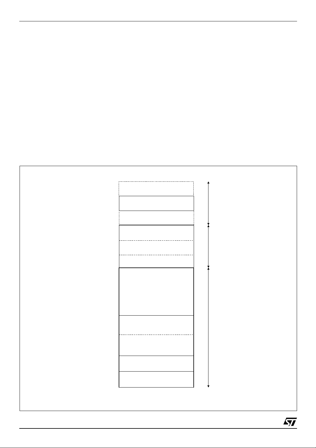
NVM is always located beginning after the first
locations of the addressing space. RAM banks are
always located after NVM.
NVM is organized in acco rdance to the following
blocks (see Figure 3.2):
■
Reset Vector block
(from address 0 to 2)
contains an absolute jump instruction to the first
user program instruction. The Assembler tool
automatically fills these locations with correct
data.
■
Interrupt Vectors block
(from location 3 up to
32) contains the interrupt vectors. Each address
is composed of three bytes (the jump opcode
and the 16 bit address). Interrupt vectors are set
by using IRQ pseudo-instruction (see the
Programming Manual).
Figure 3.2 Program/Data Memory Organization
FFFFh
~~
307Fh
OPTION BYTES
3000h
~~
20FFh
SYSTEM STACK
■
Mbfs Setting block
(just after the interrupt
vectors) contains the coordinates of the vertexes
of every Mbf defined in the program. The last
address that can be assigned to this block is
1023. This area is dynamically assigned
according to the size of the fuzzy routines. The
memory area that remains unused, if any, is
assigned to the Program Instructions block.
■
The Program Instructions block
(just after the
last Mbf data through the last NVM address)
contains the instruction of the user program and
the permanent data.
■
Option bytes block
(from location 3000h to
307Fh) is the addressing space reserved for the
option bytes. In ST 52F510/F513/F514, o nly the
location from 3000h to 3007h are used.
SPACE NOT
ADDRESSABLE
2000h
0400h
0021h
0003h
0000h
DATA
USER STACK
PROGRAM INSTRUCTIONS
AND PERMANENT DATA
PROGRAM INSTRUCTIONS
AND PERMANENT DATA
MEMBERSHIP FUNCTIONS
PARAMETERS
INTERRUPT VECTORS
RESET VECTOR
RAM
BENCH
NON
VOLATILE
MEMORY
22/106
Page 23
ST52F510/F513/F514
Flash and EEPROM are pr ogrammed electrically
just applying the supply voltage (2.7 V to 5.5 V) and
it is also erased electrically; this feature allows the
user to easily reprogram the memory without
taking the device off from the board (In Situ
Programming ISP). Data and commands are
transmitted through t he I
2
C serial communicatio n
protocol. Data can also be written run-time with the
In Application Programming (IAP)
NVM can be locked by the user during the
programming phase, in orde r to prevent external
operation such as rea ding the program code an d
assuring protection of user intellectual property.
Flash and EEPROM pages can be protected by
unintentional writings.
The operations that can be performed on the NVM
during the Programmin g Phase, ISP and IAP ar e
described in detail in the Section 4.
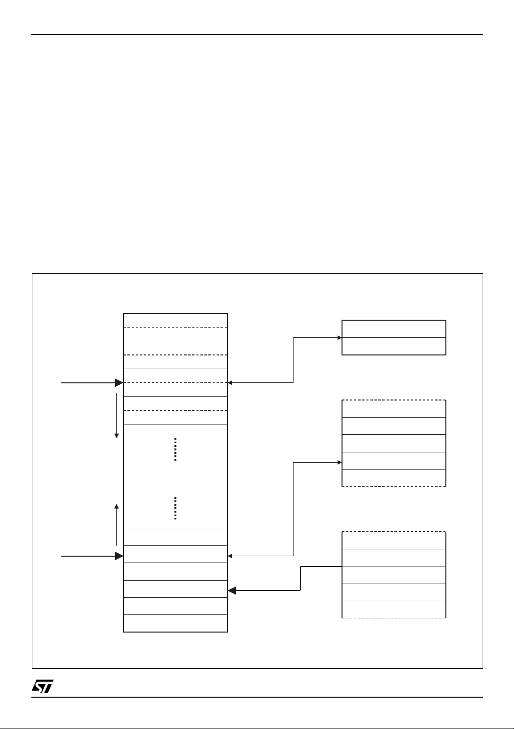
Figure 3.3 System and User Stack
RAM BENCH
20FFh
20FEh
SYSTEM STACK
POINTER
SYSTEM STACK
LEVEL 1
SYSTEM STACK
LEVEL 2
SYSTEM STACK
LEVEL 3
SYSTEM STACK
LEVEL 4
IRQ
3.4 System and User Stacks
The System and User Stacks are located in the
Program/Data memory in the RAM benches.
System Stacks are used to push the Program
Counter (PC) after an Interrupt Request or a
Subroutine Call. After a RET (Return from a
subroutine) or a RETI (Return from an interrupt)
the PC that is saved is popped from the stack and
restored. After an inter rupt request, the flags are
also saved in a r eserved s tack insi de the cor e, so
each interrupt has its own flags.
The System Stack is located in the last RAM bench
starting from the last address (255) inside the
bench page. The System Stack Pointer (SSP) can
be read and modified by the user. For each level of
stack 2 bytes of the RAM are used. The SSP points
to the first currently available stack position. When
a subroutine call or interrupt request occurs, the
content of the PC is stored in a couple of locations
pointed to by the SSP that is decreased by 2.
PROGRAM COUNTE R
RETI
LOCATION ADRESS
PAGE NUMBER
REGISTER FILE
LSB
MSB
USER STACK
POINTER
2001h
2000h
USER DATA
USER STACK LEVEL 4
USER STACK LEVEL 3
USER STACK LEVEL 2
USER STACK LEVEL 1
PUSH X
POP X
REGISTER X
CONFIGURATION REGISTERS
USER STACK TOP LSB
USER STACK TOP MSB
23/106
Page 24

ST52F510/F513/F514
When a return occurs (R ET or RETI instruction),
the SSP is increas ed by 2 and the data stored in
the pointed locations co uple is restored back into
the PC.
The current SSP can be read and write in the
couple of Configuration Reg isters 44 02Ch (MSB :
page number, always 32 020h) and 45 02Dh (LSB:
location address) ( see Figure 3.3). In ST52F51 0/
F513/F514 the user can only consider the LSB
because the MSB is always the same.
The User Stack is used to s tore user data and is
located beginning fr om a RAM bench locati on set
by the user (USTP) by writing the couple of
Configuration Registers 5 005h (MSB: page
number) and 6 005h (LSB: location address) (see
Figure 3.3). Register 5, which is the page number,
must always be set to a va lue between 32 (020h)
and 255 (0FFh): values higher than 32 always
address RAM on page 32.
Note: In ST52F510/F513/F514 MSB doesn’t have
to be set or read because the RAM is only 256
bytes. The LSB of the user stack is equal to 0 at
reset. The LSB of the system stack is equal to 255
at reset.
This feature allows a flexible use of the User Stack
in terms of dimensi on and to avoid ove rlaps. The
User Stack Pointer (USP) points to the first
currently availab le stack location. When the user
stores a byte value contain ed in the Register File
by using the PUSH in structi on, the valu e is store d
in the position pointed to by the USP that is
increased (the User Stack o rder is oppo site to the
System Stack one). Wh en the user takes a valu e
from the User Stack with the POP inst ruction, the
USP is decreased and the value pointed to is
copied in the specified Register File location.
By writing the USTP, the new address is
automatically written in the USP. The current USP
can be read from the Input Registers 11 0Bh
(MSB: page number, always 32 020h) and 12 0Ch
(LSB: location address) (see Figure 3.3). In
ST52F510/F513/F514 the user can only consider
the LSB because the MSB is always the same.
Note: The user must pay close attention to avoid
overlapping user and Stacks data. The User Stack
Top location and the System Stack Pointer should
be configured with c are in order to have enough
space between the two stacks.
3.5 Input Registers
The ST52F510/F513/F514 Input Regis ters bench
consists of a file of 8-bit regis ters containing data
or the status of the p eripherals. For exam ple, the
Input Registers contain data converted by the
ADC, Ports, serial communication peripherals,
Timers, etc.
The Input Registers can be accessed by using the
LDRI instruction that loads the specified Register
File address with the contents of the specified
Input Register. See the Programming Manual for
further details on this instruction. The Input
Registers are read-only registers.
In order to simplify the concept, a mnemonic name
is assigned to each register. The same name is
used in Visual FIVE devel opmen t tools. The list of
the Input Registers is shown in Table 3.1.
3.6 Output registers
The ST52F510/F513/F514 Output Registers
bench consists of a file of 8-bit registers containing
data sent to the Periphe rals and the I/O Port s (for
example: Timer Counter s, data to be transmitted
by the serial communication peripherals, data to be
sent to the Port pins in output, etc.).
The registers are located inside the Peripherals
and Ports, which allow flex ibility and modul arity in
the design of new family devices.
The Output Registers are write only. In order to
access the configuration Register the user can use
the following instructions:
■ LDPI: loads the immediate value in the specified
Output Register.
■ LDPR: loads the contents of the specified
Register File location into the output register
specified. This instruction allows computed data
to be sent to Peripherals and Ports.
■ LDPE direct: loads th e c ont ents of the sp ec ifi ed
Program/Data Memory l ocation into the output
register specified. This instruction allows data to
be sent to Peripherals and Ports from a table.
■ LDPE indirect: loads the contents of the
Program/Data Memo ry location whose address
is contained in the specified Register File
location into the output reg ister specified. This
instruction allows da ta to be se nt to Per ipheral s
and Ports from a table pointed to by a register.
See the Programming manual for further details
about these instructions.
In order to simplify the concept, a mnemonic name
is assigned to each register. The same name is
used in Visual FIVE devel opmen t tools. The list of
the Output Registers is shown in Table 3.2.
24/106
Page 25

ST52F510/F513/F514
3.7 Configuration Registers & Option Bytes
The ST52F510/F513/F514 Configuration
Registers bench con si st s o f a f il e of 8- bit r egi ste rs
that allows the configuration of all the ICU blocks.
The registers are located inside the block they
configure in order to ob tain greater flexibility and
modularity in the design of new f amily devices. In
the Configuration Registers, each bit has a
peculiar use, so the logic level of each of them
must be considered.
Some special c onfig urati on dat a, that needs to b e
load at the start-up and not further changed, are
stored in Option Bytes. These are loaded only
during the device program ming phase. See Tabl e
3.3 and Section 4 for a d etailed descr iption of the
Option Bytes.
The Configuration Registers are readable and
writable; the address es refer to the sam e register
both in read and in writ e. In order to access the
Configuration Register the user can work in
several modes by utilizing the following
instructions:
■ LDCI: loads the immediate value in the
Configuration Register specified and is the most
commonly used to write configuration data.
■ LDCR: loads the Configuration Register
specified with the contents of the specified
Register File location, allowing a parametric
configuration.
■ LDCE: loads the Configuration Register
specified with the contents of the specified
Program/Data Memory location, allowing the
configuration data to be taken from a table.
■ LDCNF: loads the Register File location
specified with the c ontents of the Con figuration
Register indicated, allowing for the inspection of
the configuration of the device (permitting s afe
run-time modifications).
In order to simplify the concept, a mnemonic name
is assigned to each register. The same name is
used in Visual FIVE devel opmen t tools. The list of
the Configuration Registers is shown in Table 3.4.
25/106
Page 26

ST52F510/F513/F514
Table 3.1 Input Registers
Mnemonic Description Address
PORT_A_IN Port A data Input Register 0 00h
PORT_B_IN Port B data Input Register 1 01h
PORT_C_IN Port C data Input Register 2 02h
- Not Used 3 03h
- Not Used 4 04h
SPI_IN Serial Peripheral Interface data Input Register 5 05h
I2C_IN
I2C_SR1
I2C_SR2
2
C Interface data Input Register
I
2
I
C Interface Status Register 1
2
I
C Interface Status Register 2
606h
707h
808h
- Not Used 9 09h
- Not Used 10 0Ah
USP_H User Stack Pointer (MSB) 11 0Bh
USP_L User Stack Pointer (LSB) 12 0Ch
- Not Used 13-2 0
0Dh-
014h
PWM0_COUNT_IN_H PWM/Timer 0 Counter Input Register (MSB) 21 015h
PWM0_COUNT_IN_L PWM/Timer 0 Counter Input Register (LSB) 22 016h
PWM0_STATUS PWM/Timer 0 Status Register 23 017h
PWM0_CAPTURE_H PWM/Timer 0 Capture Register (MSB) 24 018h
PWM0_CAPTURE_L PWM/Timer 0 Capture Register (LSB) 25 019h
PWM1_COUNT_IN_H PWM/Timer 1 Counter Input Register (MSB) 26 01Ah
PWM1_COUNT_IN_L PWM/Timer 1 Counter Input Register (LSB) 27 01Bh
PWM1_STATUS PWM/Timer 1 Status Register 28 01Ch
PWM1_CAPTURE_H PWM/Timer 1 Capture Register (MSB) 29 01Dh
PWM1_CAPTURE_L PWM/Timer 1 Capture Register (LSB) 30 01Eh
- Not Used 31-3 5
SCI_IN Serial Communication Interface RX data Input Register 36 024h
SCI_STATUS Serial Communication Interface Status Register 37 025h
FLAGS Flag Register 38 026h
AD_OVF 10-bit A/D Converter Overflow Register 39 027h
IAP_SR In Application Programming Status Register 40 028h
26/106
01Fh-
023h
Page 27

ST52F510/F513/F514
Table 3.1 Input Registers
Mnemonic Description Address
CHAN0_H 10-bit A/D Converter Channel 0 data Input Register (MSB) 41 029h
CHAN0_L 10-bit A/D Converter Channel 0 data Input Register (LSB) 42 02Ah
CHAN1_H 10-bit A/D Converter Channel 1 data Input Register (MSB) 43 02Bh
CHAN1_L 10-bit A/D Converter Channel 1 data Input Register (LSB) 44 02Ch
CHAN2_H 10-bit A/D Converter Channel 2 data Input Register (MSB) 45 02Dh
CHAN2_L 10-bit A/D Converter Channel 2 data Input Register (LSB) 46 02Eh
CHAN3_H 10-bit A/D Converter Channel 3 data Input Register (MSB) 47 02Fh
CHAN3_L 10-bit A/D Converter Channel 3 data Input Register (LSB) 48 030h
CHAN4_H 10-bit A/D Converter Channel 4 data Input Register (MSB) 49 031h
CHAN4_L 10-bit A/D Converter Channel 4 data Input Register (LSB) 50 032h
CHAN5_H 10-bit A/D Converter Channel 5 data Input Register (MSB) 51 033h
CHAN5_L 10-bit A/D Converter Channel 5 data Input Register (LSB) 52 034h
CHAN6_H 10-bit A/D Converter Channel 6 data Input Register (MSB) 53 035h
CHAN6_L 10-bit A/D Converter Channel 6 data Input Register (LSB) 54 036h
CHAN7_H 10-bit A/D Converter Channel 7 data Input Register (MSB) 55 037h
CHAN7_L 10-bit A/D Converter Channel 7 data Input Register (LSB) 56 038h
27/106
Page 28

ST52F510/F513/F514
Table 3.2 Output Registers
Mnemonic Description Address
PORT_A_OUT Port A data Output Register 0 00h
PORT_B_OUT Port B data Output Register 1 01h
PORT_C_OUT Port C data Output Register 2 02h
- Not Used 3 03h
- Not Used 4 04h
SPI_OUT Serial Peripher al Inte rfa ce data Outp ut Regis te r 5 05h
I2C_OUT
PWM0_COUNT_OUT_H PWM/Timer 0 Counter Output Register (MSB) 7 07h
PWM0_COUNT_OUT_L PWM/Timer 0 Counter Output Register (LSB) 8 08h
PWM0_RELOAD_H PWM/Timer 0 Reload Register (MSB) 9 09h
PWM0_RELOAD_L PWM/Timer 0 Reload Register (LSB) 10 0Ah
PWM1_COUNT_OUT_H PWM/Timer 1 Counter Output Register (MSB) 11 0Bh
PWM1_COUNT_OUT_L PWM/Timer 1 Counter Output Register (LSB) 12 0Ch
PWM1_RELOAD_H PWM/Timer 1 Reload Register (MSB) 13 0Dh
PWM1_RELOAD_L PWM/Timer 1 Reload Register (LSB) 14 0Eh
SCI_OUT Serial Communication Interface TX data Output Register 23 017h
2
C Interface data Output Register
I
606h
Table 3.3 Option Bytes
Mnemonic Description Address
OSC_CR Oscillator Control Register 0 00h
CLK_SET Clock Parameters 1 01h
OSC_SET Oscillator Set-Up 2 02h
PLDV_CR Programmable Low Voltage Detector Control Register 3 03h
WDT_EN HW/SW Watchdog selector 4 04h
PG_LOCK First Page Write Protected 5 05h
PG_UNLOCK First Page not Write Protected 6 06h
WAKEUP Wake Up from Halt Time 7 07h
28/106
Page 29

ST52F510/F513/F514
Table 3.4 Configuration Registers
Mnemonic Description Address
INT_MASK Interrupt Mask Register 0 00h
INT_POL Interrupts Polarity 1 01h
INT_PRL_H Interrupt Priority Reg ist er (hig he r priority ) 2 02h
INT_PRL_M In te rru pt Pri orit y Regist er (me di um prior ity) 3 03h
INT_PRL_L Interrupt Priority Register (lower prior ity) 4 04h
USTP_H User Stack Top Pointer (MSB) 5 05h
USTP_L User Stack Top Pointer (LSB) 6 06h
WDT_CR Watchdog Configurati on Re gis te r 7 07h
AD_CR1 10-bit A/D Converter Control Register 1 8 08h
PWM0_CR1 PWM/Timer 0 Configuration Register 1 9 09h
PWM0_CR2 PWM/Timer 0 Configuration Register 2 10 0Ah
PWM0_CR3 PWM/Timer 0 Configuration Register 3 11 0Bh
PWM1_CR1 PWM/Timer 1 Configuration Register 1 12 0Ch
PWM1_CR2 PWM/Timer 1 Configuration Register 2 13 0Dh
- Not Used 14 0Eh
- Not Used 15 0Fh
I2C_CR
I2C_CCR
I2C_OAR1
I2C_OAR2
2
I
C Interface Control Register
2
I
C Interface Clock Control Register
2
I
C Interface Own Address Register 1
2
I
C Interface Own Address Register 2
16 010h
17 011h
18 012h
19 013h
SPI_CR Serial Peripheral Inte rfa ce Con trol Regi ste r 20 014h
SPI_STATUS_CR Serial Peripheral Inte rfa ce Con trol-Status Register 21 015h
SCI_CR1 Serial Communication Interface Control Register 1 22 016h
SCI_CR2 Serial Communication Interface Control Register 2 23 017h
PORT_A_PULLUP Port A Pull Up enable/disable Register 24 018h
PORT_A_OR Port A Option Register 25 019h
29/106
Page 30

ST52F510/F513/F514
Table 3.4 Configuration Registers
Mnemonic Description Address
PORT_A_DDR Port A Data Direction Register 26 01Ah
PORT_A_AF Port A Alternate Function selection Register 27 01Bh
PORT_B_PULLUP Port B Pull Up enable/disable Register 28 01Ch
PORT_B_OR Port B Option Register 29 01Dh
PORT_B_DDR Port B Data Direction Register 30 01Eh
PORT_B_AF Port B Alternate Function selection Register 31 01Fh
PORT_C_PULLUP Port C Pull Up enable/disable Register 32 020h
PORT_C_OR Port C Option Register 33 021h
PORT_C_DDR Port C Data Direction Register 34 022h
PORT_C_AF Port C Alternate Function selection Register 35 023h
- Not Used 36-4 2
SCI_CR3 Serial Communication Interface Control Register 3 43 02Bh
SSP_H System Stack Pointer (MSB) 44 02Ch
SSP_L System Stack Pointer (LSB) 45 02Dh
CPU_CLK CPU Clock Prescaler 46 02Eh
AD_CR2 10-bit A/D Converter Control Register 2 47 02Fh
024h-
02Ah
30/106
Page 31

ST52F510/F513/F514
4 MEMORY PROGRAMMING
ST52F510/F513/F514 provides an on-chip user
programmable non-vo latile memory, whic h allows
fast and reliable storage of user data.
Program/Data Memory addressing space is
composed by a Singl e Vol tag e Fl ash Memory and
a RAM memory bench. The ST52F513/514
devices also have a Data EEPROM bench to store
permanent data with long term retention and a high
number of write/erase cycles.
All the Program Data memory addresses can
execute code, including RAM and EEPROM
benches.
The memory is programmed by setting the V
equal to V
through the I
. Data and commands are transmitted
dd
2
C serial communication protocol. The
pp
pin
same procedure is used to perform “In-Situ” the
programming of the dev ice after it is mounted in
the user system. Data can also be written in runtime with the In-Application Programming (IAP).
The Memory can be locked by the user dur ing the
programming phase, in orde r to prevent external
operation such as rea ding the program code an d
assuring protection of user intellectual property.
Flash and EEPROM pages can be protected by
unintentional writings.
Remark: the memory contents are protected by
the Error Correction Code (ECC) algorithm that
uses a 4-bit redundancy to correct one bit errors.
Warning: when entering the ISP, the default
values for Option Bytes are considered, so a
Voltage Supply higher than the PLVD lower
threshold must be applied to program the device.
4.1 Program/Data Memory Organization
The Program/Data Memory is organized as
described in Sec tion 3.3. The var ious sales type s
have different amounts of each type of memory.
Table 4.1 describes the me mory bench es amount
and page allocation for each sales type.
The addressing spaces are organ ized in pag es of
256 bytes. Each page is composed by blocks of 32
bytes. Memory programming is performed one
block at a time in order to speed-up the
programming time (about 2.5 ms per block).
The whole location address is composed as
follows:
15 87 54 0
Page address Block address address inside the block
Table 4.1 Sales Type Memory Organization
Flash Memory RAM Memory EEPROM Memory
Device
Amount Pages Amount Page Amount Page(s)
ST52F510c2p6 4096 bytes 0 to 15 256 bytes 32 - ST52F510c3p6 8192 bytes 0 to 31 256 bytes 32 - ST52F513c2p6 3840 bytes 0 to 14 256 bytes 32 256 bytes 15
ST52F513c3p6 7936 bytes 0 to 30 256 bytes 32 256 bytes 31
ST52F514c1p6 4096 bytes 0 to 15 256 bytes 32 1024 bytes 16-19
ST52F514c3p6 4096 bytes 0 to 15 256 bytes 32 4096 bytes 16-31
legend:
c:
Y=16 pins, F=20 pins, G=28 pins, K=32/34 pin
p: B=DIP, M=SO, T=TQFP
31/106
Page 32

ST52F510/F513/F514
4.2 Memory Programming
The Programming procedure writes the user
program and data into the Flash Memory,
EEPROM and Option Bytes. The programming
procedures are entered by setting the V
equal to V
and releasing the Re set signal. The
dd
pp
pin
following pins are used in Programming mode:
■ V
PP
■ V
DD
■ V
SS
■ RESET device reset
■ SCL I
■ SDA I
used to switch to programming mode
device supply
device ground
2
C serial clock
2
C serial data
During the device progra mming , the interna l cl ock
is used, so the OSCin and OSCout pins don’t have
to be considered.
1. V
is set to V
PP
DD
2. The device is Reset (RESET=VSS)
3. The Reset is released (RESET=V
DD
)
4. The internal oscillator starts at 10 MHz
5. The memory is turned on
6. The I
7. The I
2
C Interface and Ports are initialized
2
C Interface is configured to work as
Slave, Receiver, 7-bit addre ss and waits for
data
8. The Start signal is sent to the chip followed by
the Slave Address 10 100 00 and the dir ec ti on
bit set to 0 (the a ddr ess ed sl av e wa its for data). The device sends the acknowledge
9. The Programming Mode code 00000000 is
sent and acknowledged
10. A command code is sent to the device
4.2.1 Programming Mode start. The following
sequence starts the Programming Mode:
11. The proc edure re lat ed to the co mma nd i s ex ecuted
Table 4.2 Programming Mode Commands
Command Code Data in Data out Erase Description
BlockWrite 00000001 32 - Yes
ByteWrite 00000010 2 - Yes
BlockErase 00000011 1 Yes
ByteErase 00000100 1 Yes
ByteRead 00000101 1 1 -
GlobalErase 00001001 - - Yes All the memory is erased.
FastBlockWrite 00001011 32 - No
SetPage 00001100 1 - - The currently addressed page is set with the next data sent.
ReadData 00001101 - 1 -
Inc Bl oc k 0 00 01111 - - -
ReadStatus 00010011 - 1 -
Write the currently addressed block with the 32 bytes
following the command. The Block locations are erased
before being written.
Write the byte addressed by the next data sent in the
currently address ed page.
Erase the block address ed by 3 M SB of the next data sent
and inside the currently addressed page.
Erase the byte addres sed by t he next da ta sent an d inside
the currently addressed page.
Read the byte ad dressed by the nex t data sent and insi de
the current page. Th e read data is sent by the device after
the re-send of the Slave Address with the R/W bit changed.
Write the currently addressed block with the 32 bytes
following the command. The Block locations aren’t erased.
Read the memory location currently addressed. The re ad
data is sent by the device after the command is
acknowledged. The current memory absolute address is
post-incremented.
The current block address is incremented modulo 8
(address 0 follow s after address 7 and the Page is postincremented)
This command is followed by a status data byte. Mostly
used in error condition and to check if the device is locked
32/106
Page 33

Figure 4.1 Commands and Data Communication Sequences
Programming mode start sequence
S 10100000 A 00000000 A
Command
A Data1 A ..... DataN AP
Execution of commands for writing data:
Command
A Data1 A ..... DataN A
Command
A Data1 A ..... DataN AP
Execution of commands for reading data:
Command
A Address A P S 10100001 A Data read NA P
S=Start, P=Stop, A=Acknowledge, NA=Non-acknowledge
From Slave to Master From Master to Slave
ST52F510/F513/F514
The generic procedure of commands execution,
with the data communicati on in both directions is
displayed in Figure 4.1.
Remark: the Slave Address 1010000 must be sent
after a Stop (i.e. each time the data direction
changes, to specify the R/W bit). For example: if a
command to send data to the device has been
executed, a command for receiving dat a must be
followed by the slave address and the R/W bit must
be set to 1. The Progr ammin g Mode code doesn’ t
need to be specified again .
Warning: After entering the Programming Mode,
the currently pointed address is the Page 48, Block
3, byte 0 (Lock Byte).
The list of the available commands in
Programming Mode is showed in Table 4.2
4.2.2 Fast Programming procedure. The
fastest way to program the de vice memory is the
use of the
FastBlockWrite
command. The following
procedure can be used to write the memory with a
new program and new data, sta rting from the first
memory location:
1. The Programming Mode is entered with the
sequence described above
2. The memory is erased ( all bits are put to 0)
with the
GlobalErase
command. The d evice
holds the SCL line low, releasing it after the
command is completed (about 2 ms). This
command also unlocks the device if locked.
3. The
FastBlockWrite
command is sent and the
device acknowledge s it
4. The 32 bytes of data to be written in the first
memory Block are sent in a sequence. The
device acknowledges each of them
5. After the device acknowledges the 32nd byte,
it holds the SCL line until the parallel writing of
the 32 byte is completed (about 2.5 ms)
6. The Block Pointer is incr emented by sending
the
IncBlock
command
7. The procedure is repeated from point 3 until
there is data to be sent to the memory
Note: the Block Pointer assumes v alues between
0 to 7 (there are 8 blocks in a page). When the
Block Pointer is equal to 7, the IncBlock command
puts this pointer to 0 and increments the Page
Pointer. The Page Pointer, after page writing is
completed, does’ t have to be incremented in the
procedure above described.
4.2.3 Random data writing. A single byte can be
written in a specified memory location by using the
following procedure:
1. The Programming Mode is entered with the
sequence described in Section 4.2.1
2. The
SetPage
command is sent, followed by
the page number wh ere the data should be
written
3. The
ByteWrite
command is sent fol lowed by
two bytes
4. The first bytes that follows the ByteWrite command is the address ins ide the pointed pa ge
where the data must be written.
5. The second byte is the data to be written
6. The device held the SCL line low until the data
is not stored in the memory (a bout 4.5 ms: 2
ms for erasing and 2.5 for writing)
33/106
Page 34

ST52F510/F513/F514
A similar procedure ca n be used to write a single
block:
1. The
SetPage
command is sent, f ollowed by
the page number where the data should be
written
2. The
IncBlock
command is sent as many times
as the block number inside the pa ge (for example: to address the block 3 the
IncBlock
must be sent 3 times)
3. The
WriteBlock
command is sent fol lowed by
the 32 data bytes to be written.
4. After the 32th b yte is sent, the device ho lds
the SCL line low until all the data are not
stored in the memory (abo ut 4. 5 ms : 2 ms for
erasing and 2.5 for writing: th e same time for
a single byte)
The procedures described previously can be
repeated as many time as needed , without exiting
from Programming Mode or re-sending the Slave
Address ag ain.
Figure 4.2 Programming Procedures
Fast Programming Procedure
S 10100000 A 00000000 A
GlobalErase
The commands ByteEr ase and BlockErase, used
instead of ByteWrite and BlockWrite, erase (put all
bit to 0) the specified memory location or block.
4.2.4 Option Bytes Programming. The Option
Byte addresses cannot be accessed with a
sequential procedure like the one described in
Section 4.2.2. Actually, the pointers are
automatically in cremented up to the last bl ock or
address in page 31. A further increment sets all the
pointers to 0.
The Option Byte addre sses (located at page 48,
block 0, addresses 0- 7) must be accessed wi th a
direct addressing proc edure as the o ne describ ed
in Section 4.2.3.
If the Fast Programming procedure is used, it must
be followed by a Random Block Writing procedure
to program the Option Bytes. The other 24 bytes of
the block can be written with dummy or user
values. The blocks 0, 1, 2 and 3 of Page 48 can be
used for writing data as well (see Section 4.5) and
for locking the device (see Section 4.4).
A
FastBlockWrite
A Data0 A .....
..... Data31
IncBlock
A
FastBlockWrite
A ..... Data31 A ..... ..... Data31 AP
A
Random Byte Writing Procedure
.....
SetPage
A Page Address A
ByteWrite
A Byte Address ADataA
Random Block Writing Procedure
SetPage
.....
..... Data31
A Page Address A
A
Command
.....
IncBlock
A .....
IncBlock
Option Byte Writing Procedure
SetPage
.....
..... Dummy 0
A 00110000 A
A ..... Dummy 23 AP
WriteBlock
A Option Byte 0 A ..... Option Byte 7 A .....
S=Start, P=Stop, A=Acknowledge, NA=Non-acknowledge
From Slave to Master From Master to Slave
A
BlockWrite
Command
A Data0 A .....
.....
34/106
Page 35

Figure 4.3 Reading and Erasing Procedures
Fast Reading Procedure
S 10100000 A 00000000 A
A
..... S 10100000
ReadData
ReadData
A P S 10100001 A Data read NA P ..... Data read NA P
Random Byte Reading Procedure
.....
SetPage
A Page Address A
ByteRead
ST52F510/F513/F514
A P S 10100001 A Data read NA P .....
A By te Ad dre ss A P S 10100 001 A .....
Data read NA P S 10100000 A
.....
Command
.....
Byte Erasing Procedure
.....
SetPage
A Page Address A
ByteErase
A Byte Address A
Command
.....
Block Erasing Procedure
SetPage
.....
(*) Block address is specified by the 3 most significative bits of the whole given address (less significative bits are don’t care)
A Page Address A
BlockErase
A Block Address (*) A
Command
.....
S=Start, P=Stop, A=Acknowledge, NA=Non-acknowledge
From Slave to Master From Master to Slave
4.3 Memory Verify
To verify the memor y conten ts or just to read par t
of data stored in memo ry, the
ReadData
command can be used. The first
ByteRead
and the
instruction needs t he specificati on of the address;
the second one allows the sequential reading of
consecutive memory locations.
Since the device is “Slave” for the I
2
C protocol,
after receiving a comma nd for reading, it mus t be
configured as Slave Tran smitter to se nd the data.
In order to do so, the Slave Address (1010000)
must be sent again with the R/W b yte set to 1 , as
stated by the communication protocol.
5. The Slave Address with the R/W byte set to 1
(10100001) is sent. The device receives the
Slave Address and acknowledges it.
6. The device sends the data to be read in the
serial data line SDA. The current absolute address is post-incremented.
7. The Master device doesn’t send the acknowledge and generates a stop condition.
8. To read the next data, the Master generates a
Start condition followed by the Slave Address
with the R/W byte set to 0 (10100000). The
4.3.1 Fast read procedure. The memory can be
read sequentially by using the following procedure:
1. The Programming mode is entered with the
sequence described in Section 4.2.1
2. The pointers address the memory location 0
3. The
ReadData
command is sent a nd the de-
vice acknowledges it.
4. The Master generates a Stop condition followed by a Start condition
device receives the Slave Address and acknowledges it.
9. The sequence restarts from point 3 until there
is data to be read.
Remark: for the same reasons explained in
Section 4.2.4 the Option Bytes cannot be read with
this procedure: they can be read with a direct
addressing procedur e as the one explain ed in the
next section.
35/106
Page 36

ST52F510/F513/F514
4.3.2 Random data reading. To read a spe cified
memory location, the following procedure should
be used:
1. The Programming mode is entered with the
sequence described in Section 4.2.1
2. The
SetPage
command is sent, followed to
the page number where the data to be read is
located
3. The
ByteRead
command is sent, followed by
an address inside the page
4. The Master generates a Stop condition followed by a Start condition
5. The Slave Address with the R/W byte set to 1
(10100001) is sent. The device receives the
Slave Address and acknowledges it.
6. The device sends the data to be read in the
serial data line SDA.
7. The Master device doesn’t send the acknowl-
edge and generates a stop condition.
8. To send the next command, the Master
should generate a Sta r t c onditi on f oll owe d by
the Slave Address with the R/ W by te set to 0
(10100000).
Figure 4.4 Device Lock Procedure
4.4 Memory Lock
The Program/Data Memory space can be locked to
inhibit the reading of contents and protect the
intellectual property.
To lock the device, the user must set all the bit of
the Lock Byte to ‘1’. The Lock Byt e is located on
Page 48 (030h), Block 3, byte 0 inside the block i.e.
byte 96 (060h) inside the page.
After writing 255 (0FFh) into the Lock Byte, with the
procedure described in the Section 4.2.3, the
memory is locked and th e only command al lowed
are the following:
–
GlobalErase
: this command, writi ng ‘0’ in al l the
memory, also unlock the device.
–
ReadData
: the only block that can be read is the
Block 3 in Page 48 (030h); this al low s the r ead ing of the Lock Byte a nd the ID Code locat ions
(see Section 4.5).
–
ReadStatus
: this command allows the detection
of an error co ndition in Programm ing mode op eration (s ee Se c tion 4.6). It can als o b e us ed t o
check if the device is locked. The most significative bit return the Lock Bit (0=unlocked,
1=locked).
Remark: the Lock Byte is ch ecked wh en entering
the Programming Mode. For this reason after
writing the Lock Byte, all the commands can be
carried out until the Programming mode is exited.
Device Lock Procedure
.....
SetPage
A 00110000 A
ByteWrite
A 01100000 A 11111111 A
Device Lock and ID Code Writing Procedure
SetPage
.....
..... 11111111
A 00110000 A
A ID Code 1 A ID Code 2 A ..... ID Code 31 A
IncBlock
A
IncBlock
Device Lock Reading Procedure
ReadStatus
.....
(*) The most significative bit return the Lock Bit (0=unlocked, 1=locked)
A P S 10100001 A Status Byte (*) NA P S 10100000 A
S=Start, P=Stop, A=Acknowledge, NA=Non-acknowledge
From Slave to Master From Master to Slave
A
IncBlock
A
BlockWrite
Command
Command
.....
Command
.....
A .....
.....
36/106
Page 37

Figure 4.5 Error Handling Procedure
Wrong command/data case handling:
Wrong Command/Data A Command/Data NA
ReadStatus
S=Start, P=Stop, A=Acknowledge, NA=Non-acknowledge
From Slave to Master From Master to Slave
ST52F510/F513/F514
A P S 10100001 A Status Byte NA P
When the device is locked, if mem ory reading is
attempted, with the exception of the Lock Byte and
ID Code block, the devic e returns no d ata and an
error sequence. If mem ory writing is att empted in
any memory location, the devi ce doe sn’t c arry o ut
the command and returns an error sequence.
To unlock the device the
GlobalErase
command
must be executed before any writing or reading
command.
4.5 ID Code
Block 3 on Page 48 (030h) c an also be read i f the
device is locked. The firs t byte of the block is th e
Lock Byte, the oth er 31 locations are available to
the user for writing data, as for example
identification codes to distinguish the firmware
version loaded in the device.
The ID Code must be written before locking the
device: after the device is locked it can only be
read. The use of the Block writing procedure is the
fastest way: both the ID Co de and th e Lock bytes
are written together. The loc k Bytes are sent first
and then the 31 bytes of ID Code follow.
The blocks 0, 1 and 2 on P ag e 48 can be also be
used for writing data, but they cannot be accessed
when the device is locked.
Note: the ID Code cannot be modified if the device
is locked: it can only be read.
4.6 Error cases
If a wrong command or data is sent to the dev ice,
it generates an error conditio n by not sending the
acknowledge after the first successive data or
command. Figure 4.5 shows the error sequence.
The error case can be handled by using the
ReadStatus
command. This command can be sent
after the error condition is detected; the device
returns a Status Byte containing the error code.
The
ReadStatus
command sequence is showed in
Figure 4.5. The list o f the erro r cod es is il lust rated
in Table 4.3.
Remark: after the ReadStatus command
execution or after any error, the Start Sequence
must be carried out before sending a new
command.
The Most Significative Bit of the error codes
indicates (when set to ‘1’) that the memory is
locked. When a command, that is not allowed
when the memory is locked, is sent, the “
Allowed”
code is sent. If a not her cod e is sen t with
Not
the MSB to ‘1’ it indicates that the error condition is
not caused by the memo ry lock, but by the event
related with the code sent.
Warning: when the data writing into a non existing
location is attempted, no error condition is
generated. The us er must take c are in specif ying
the correct page address.
Table 4.3 Error codes
Name Code Description
Device Locked xyyyyyyy x=lock bit (1=device locked), yyyyyyy=error code
Wrong Direction x0000001 A transmit direction, not correct in the running sequence, has been set
Stop Missed x0000010 The Master missed generating a necessary Stop Condition
Data Missing x0000011 The Master missed to send necessary data to the device
Receive Error x0000100 The data sent by the Master hasn’t been received correctly by the device
Wrong Command x0000101 The Master sent a wrong command code
Not Allowed x0000110 A command not allowed when the device is locked has been sent
Wrong Mode x0010000 A code different form the Programming mode code (00000000) has been sent
37/106
Page 38

ST52F510/F513/F514
4.7 In-Situ Programming (ISP)
The Program/Data Memory can be programmed
using the ISP mode. This mode a llows the d evice
to be programmed when i t is mounted in th e user
application board.
This feature can be implemented by adding a
minimum number of components and board
impact.
The programming procedur es and pins used are
identical to the ones described before for the
standard Programming Mode. All the features
previously describ ed in this ch apte r are ap pl ic abl e
in ISP mode.
If RESET, SCL and SDA pins are used in the user
application board for other purposes, it is
recommended to u se a serial resistor to a void a
conflict when the other devices force the signal
level.
The ISP can be applied by using the standard tools
for the device programming.The ISP can be
applied by using the standard too ls for the device
programming. The ST52F510 Sta rter Kit supplies
a cable to perform the ISP. The user application
board should supply a suited connector type for the
cable (see Starter Kit User Manual).
4.8 In-Application Programming (IAP)
The In Application Programming Mode (IAP)
allows the writing of user data in the Flash and
EEPROM memories when the user program is
running.
There are two ways to write data in IAP mode:
single byte write and Block wr ite . Bot h procedures
take about 4.5 ms to complete the writing: the
Block write allows the writing of 32 byte in parallel.
Remark: du ring data writing , the execution of th e
user program is stopped until the procedure is
completed. Interrupt requests stop the writing
operation and the data may be not stor ed. The bit
ABRT in the IAP_SR Input register signals that the
data writing hasn’t been completed. To assure
writing completion, the user should globally disable
the interrupts (UDGI instruction) before starting
IAP data writing.
4.8.1 Single byte write. Writing of a single byte in
the Non-Volatile Program/Data memory is
performed by using the LDER instruction (both
direct and indirect addressi ng). The mem ory page
should be indicated before the LDER instruction
with the PGSET or PGSE TR ins tructio n. Th e byte
address inside the pa ge is speci fied by the LDE R
instruction itself.
As soon as the instruction is executed, the data
writing starts and is performed in about 4.5 ms.
4.8.2 Block write. This procedure allows the
writing of 32 bytes in parallel. Thes e bytes should
belong to the same block.
Before the writing in the Program/Data memory,
data must be buffered in the Register File in the
first 32 locations (0-31, 00h-020h) by using the
normal instructions to load the Register File
locations.
Then the data writing starts by using the BLKSET
instruction. The destin ation block is addr essed by
specifying the memory page with the PGSET or
PGSETR instruction before to start the writing; the
block inside the page is addressed with the
argument of the BLKSET instruction.
Example:
PGSET 5
BLKSET 4
This instruction sequence writes the contents of
the first 32 bytes of the Register File in the
locations 1408-1439 (0580h-059Fh).
Warning: the us er should be car eful in specif ying
the correct page and b lock: the addressing of an
not existing block can cause the un wanted writi ng
of a different block.
As soon as the BLKSET instruction is execut ed,
the data writing starts and is performed in about
4.5 ms.
This procedure may also be used to write few data,
taking in account that all the 32 byte are written in
the block anyway.
4.8.3 Memory Corruption Prevention.
The user can protect some pages (or all the
memory) from unintentional writings. The only
constraint is that the protected pages must be
consecutive.
Two Option Bytes allow the specification of the
page to be protected: PG_LOCK (O ption Byte 5)
and PG_UNLOCK (Opt ion Byte 6). PG_LOCK is
used to specify the first protected page;
PG_UNLOCK is used to specify the first page not
protected after the protected ones. The pages
between the two addresses are protected.
When writing in a protected page is attempted, the
procedure is aborted and the bit PRTCD of
IAP_SR Input register is set.
If the PG_LOCK and PG_UNLOCK have the same
value, no page is protected. By default, the two
Option Bytes are programmed with the value 0, so
the memory is not write protected by default.
In Programming Mode the protection is not
considered and the pages can be written unless
the device is locked.
38/106
Page 39

ST52F510/F513/F514
4.8.4 Option Bytes.
First Protected Page (PG_LOCK)
Option Byte 5 (05h)
Reset Value: 0000 0000 (00h)
70
LCK7 LCK6 LCK5 LCK4 LCK3 LCK2 LCK1 LCK0
Bit 7-0: LCK7-0 First Page write protected
In this register the address of first page to be
protected in writing is specified. The pages
following this one are protected up to the page
specified by the PG_UNLOCK Option Byte (not
4.8.5 Input Register.
IAP Status Register (IAP_SR)
Input Register 40 (028h) Read only
Reset Value: 0000 0000 (00h)
70
------PRTCDABRT
Bit 7-2: Not Used
Bit 1: PRTCD Page Protected
0: The writing has been completed
1: The writing has been aborted because the
page is protected.
included among the protected ones).
Bit 0: ABRT Writing operation aborted
0: The writing has been completed
First Page not Protected (PG_UNLOCK)
Option Byte 6 (06h)
Reset Value: 0000 0000 (00h)
70
UNLCK7 UNLCK6 UNLCK5 UNLCK4 UNLCK3 UNLCK2 UNLCK1 UNLCK0
1: The writing has bee n abor ted becau se an
interrupt or another unspecified cause
occurred.
The ABRT and PRTCD bits are reset after the next
successful data wr iting in the Flash of EEPROM
memory.
Bit 7-0: UNLCK7-0 First Page not write protected
In this register the address of fi rst page not write
protected after the protected ones is specified. The
pages following this one aren’t protected.
39/106
Page 40

ST52F510/F513/F514
Global Interrupt
5 INTERRUPTS
The Control Unit (CU) responds to peripheral
events and external events through its interrupt
channels.
When such events o ccur, if th e rel ated i nterrup t is
not masked and doesn’t have a pr iority order, the
current program execution can be suspended to
allow the CU to execute a specific response
routine.
Each interrupt is associated with an interrupt
vector that contains the memory address of the
related interrupt service routine. Each vector is
located in the Program /Data Memory space at a
fixed address (see Figure 3.2 Program/Data
Memory Organization).
5.1 Interrupt Processing
If interrupts are pending at the end of an arithmetic
or logic instruction, the int errupt with the highest
priority is acknowledged. When the interrupt is
acknowledged the flags and the current PC are
saved in the stacks and the associated Interrupt
routine is executed. The start address of this
routine (Interrupt Vect or) is located in three bytes
of the Program/Data Memory betwe en address 3
and 32 (03h-020h). See Table 5.1 for the list of the
Interrupt Vector addresses.
The Interrupt routine is performed as a normal
code. At the end of each instruction, the CU checks
if a higher priority interrupt has sent an interrupt
request. An Interrup t req uest with a higher prior ity
stops lower priority Interrupts. The Program
Counter and the flags are stored in their own
stacks.
With the instruction RETI (Return from Interrupt)
the flags and the Program Counter (PC) are
restored from the top of the stac ks. These stacks
have already been described in Paragraph 3.4.
An Interrupt request cannot stop fuzzy rule
processing, but only after the end of a fuzzy rule or
at the end of a logic or arithmetic instruction,
unless a Global Interrupt Disable instruction has
been executed before (see below).
Figure 5.1 Interrupt Flow
NORMAL
PROGRAM
FLOW
INTERRUPT
SERVICE
ROUTINE
INTERRUPT
RETI
INSTRUCTION
5.2 Global Interrupt Request Enabling
When an Interrupt occurs, it generates a Global
Interrupt Pending (GIP). After a GIP a Global
Interrupt Request (GIR) will be generated and
Interrupt Service Routine associated with the
interrupt with higher priority will start.
In order to avoid possible conflicts between the
interrupt masking set in the main program, or
inside high level language compiler macros, the
GIP is put in AND through the User Global Interrupt
Mask or the Macro Global Interrupt Mask (see
Figure 5.2).
The UEGI/UDGI instruction switches the User
Global Interrupt Mas k enabling/disabling the GIR
for the main program.
MEGI/MDGI instruc tions switch the Ma cro Global
Interrupt Mask on/off in order to ensure that the
macro will not be interrupted.
Figure 5.2 Global Interrupt Request
Remark: A fuzzy routine can be interrupted only in
the Main program. When a Fuzzy function is
running inside another interrupt routine an interrupt
request can cause sid e eff ec ts i n t he Co ntr ol Uni t.
For this reason, in order to use a Fuzzy function
inside an interrupt routine, the user MUST include
the Fuzzy function between an UDGI (MDGI)
instruction and an UEGI (MEGI) instruction (see
the following paragra phs), in order to disable the
interrupt request during the execution of the fuzzy
function.
40/106
Global Interrupt
Pending
User Global
Interrupt Mask
Macro Global
Request
Page 41

ST52F510/F513/F514
5.3 Interrupt Sources
ST52F510/F513/F514 manages interrupt signals
generated by the internal peripherals or generated
by software by the TRAP instruction or coming
from the Port pins. There are two kinds of
interrupts coming from th e Port pins: the NMI and
the Ports Interrupts.
NMI (Not Maskable Interrupt) is associated with pin
PA7 when it is configured as Alternate Fu nction.
This interrupt source doesn’t hav e a configurable
level priority and cannot be masked. The fixed
priority level is lower than th e software TRAP an d
higher than all the other interrupts. The NMI can be
configured to be ac tive on the rising o r the falling
edge.
The Port Interrupts sources are connected with
Port A and Port B pins . The pins bel onging to the
same Port are ass ociated with the same interru pt
vector: there is one vec tor for Port A and one for
Port B. In order to use one port pin as interrup t, it
must be configured as an interrupt source (see I/O
Ports chapter). In this manner, up to 16 Port
Interrupt sources are available. By reading the Port
the sources that belong to the same Port can be
discriminated. The Port Interrupts can be
configured to be ac tive on the rising o r the falling
edge.
Warning: changing the NMI or Port Interrupt
polarity an interrupt request is generated.
All the interrupt sources are filtered, in order to
avoid false interrupt requests caused by glitches.
The Trap instruction is something between a
interrupt and a call: it generated an interrupt
request at top priority level and the control is
passed to the associated interrupt routine which
vector is located in the fixed addresses 30-32. This
routine cannot be interrupted and it is serviced
even if the interrupts are globally disabled.
Note: Similarly to the CALL instruction, after a
TRAP the flags are not stacked.
5.4 Interrupt Maskability and Priority Levels
Interrupts can be masked by the corresponding
INT_MASK Configuration Register 0 (00h). An
interrupt is enabled when the mask bit is “1". V ice
versa, when the bit is “0” , the interrupt is masked
and the eventual requests are kept pending.
All the interrupts, with the exception of the NMI and
TRAP that have fixed level priority, have a
configurable priority lev el . The c onfi gura tion of the
priority levels is completed by writing three
consecutive Configuration Registers: INT_PRL_H,
INT_PRL_M, INT_PRL_L, addresses from 2 to 4
(02h-04h). The 24 bits of these registers are
divided into 8 group s of three bits: each group i s
associated with a priority level. The three bits of
each group are written with the code number
associated with the interrupt source. See Table 5.1
to know the codes.
Remark: The priority levels Configuration
Registers must be programmed with different
values for each 3-bit groups to avoid erroneous
operation. For this reason the Interrupt priority
must be fixed at the beginning of the main
program, because the reset values of the
Configuration Registers correspond to an
undefined configuration (all zeros). During
program execution the interrupt priority can only be
modified within the Main Program: it cannot be
changed within an interrupt service routine.
5.5 Interrupt RESET
When an interrupt is masked, all requests a re not
acknowledged and remain pending. When the
pending interrupt is enabled it is immediately
serviced. This event may be undesired; in order to
avoid this a RINT instruction may be inserted
followed by the code number that identifies the
interrupt to reset the pendi ng request. See Table
5.1 to know the codes.
Figure 5.3 Example of Interrupt Requests
PRIORITY
LEVEL
0
1
2
3
4
5
6
MAIN PROGRAM
INT2 INT0 INT4 INT1 INT3
INT2
INT0
INT2
INT1
INT2
INT3
INT4
MAIN PROGRAM
41/106
Page 42

ST52F510/F513/F514
5.6 Register Description
Interrupt Polarity Register (INT_POL)
Configuration Register 1 (01h) Read/Write
Interrupt Mask Register (INT_MASK)
Configuration Register 0 (00h) Read/Write
Reset Value: 0000 0000 (00h)
70
Reset Value: 0000 0000 (00h)
70
MSKPB MSKPA MSKI2C MSKSPI MSKSCI MSKT1 MSKT0 MSKAD
Bit 7: MSKPB Interrupt Mask Port B
0: Port B interrupt masked
1: Port B interrupt enabled
- - - RESPOL STRPOL POLPB POLPA POLNMI
Bit 7-5: Not Used
Bit 4-3: See Timer 0 Registers Description
Bit 2: POLPB Port B Interrupt Polarity
0: The Port B interrupt is triggered on the
rising edge of the applied external signal.
Bit 6: MSKPA Interrupt Mask Port A
0: Port A interrupt masked
1: The Port B interrupt is triggered on the
falling edge of the applied external signa l.
1: Port A interrupt enabled
Bit 1: POLPA Port A Interrupt Polarity
Bit 5: MSKI2C Interrupt Mask I
2
0: I
C Interface interrupt masked
2
1: I
C Interface interrupt enabled
2
C Interface
0: The Port A interrupt is triggered on the
rising edge of the applied external signal.
1: The Port A interrupt is triggered on the
falling edge of the applied external signa l.
Bit 4: MSKSPI Interrupt Mask SPI
0: SPI interrupt masked
1: SPI interrupt enabled
Bit 3: MSKSCI Interrupt Mask SCI
0: SCI interrupt masked
1: SCI interrupt enabled
Bit 2: MSKT1 Interrupt Mask PWM/Timer 1
0: Pwm/Timer 1 interrupt masked
1: Pwm/Timer 1 interrupt enabled
Bit 1: MSKT0 Interrupt Mask Pwm/Timer 0
0: Pwm/Timer 0 interrupt masked
1: Pwm/Timer 0 interrupt enabled
Bit 0: MSKAD Interrupt Mask A/D Converter
0: A/D interrupt masked
1: A/D interrupt enabled
Bit 0: POLNMI Non Maskable Interrupt Polarity
0: The NMI is trig gered on the rising e dge of
the applied external signal.
1: The NMI is triggered on the falling edge of
the applied external signal.
High Priority Register (INT_PRL_H)
Configuration Register 2 (02h) Read/Write
Reset Value: 1111 1010 (0FAh)
70
PRL23 PRL22 PRL21 PRL20 PRL19 PRL18 PRL17 PRL16
Medium Priority Register (INT_PRL_M)
Configuration Register 3 (03h) Read/Write
Reset Value: 1100 0110 (0C6h)
70
PRL15 PRL14 PRL13 PRL12 PRL11 PRL10 PRL9 PRL8
42/106
Page 43

ST52F510/F513/F514
Low Priority Register (INT_PRL_L)
Configuration Register 4 (04h) Read/Write
Reset Value: 1000 1000 (088h)
70
PRL2-PRL1: Interrupt priority level 1 (highest)
PRL5-PRL3: Interrupt priority level 2
PRL8-PRL6: Interrupt priority level 3
PRL11-PRL9:Interrupt priority level 4
PRL14-PRL12: Interrupt priority level 5
PRL7 PRL6 PRL5 PRL4 PRL3 PRL2 PRL1 PRL0
PRL17-PRL15: Interrupt priority level 6
PRL20-PRL18: Interrupt prioritylevel 7
These three register are used to configure the
priority level of each in terrupt source. The 24 bits
PRL23-PRL21: Interrupt priority level 8 (lowest)
of these registers (PRL24-PRL0) are divided into 8
groups of three bits: each group is associated with
a priority level (from level 1, the highest, to level 8,
the lowest: level 0 is fixe d for the NMI that c an be
interrupted only by the TRAP) . The three bits of
each group are written with the code number
associated with the interrupt source (see Table
Example: writing the code 110 into PRL8-PRL6
bits the priority l evel 3 is assigned to t he Port A
Interrupt.
Warni ng: the Priority Level configuration registers
must be always configured.
5.1).
Table 5.1 Interrupt sources paramethers
Interrupt Source Priority type PRL code RINT code Maskable Vector Addresses
A/D Converter Programmable 000 0 Yes 3-5 (03h-05h)
PWM/Timer 0 Programmable 001 1 Yes 6-8 (06h-08h)
PWM/Timer 1 Programmable 010 2 Yes 9-11 (09h-0Bh)
SCI Programmable 011 3 Yes 12-14 (0Ch-0Eh)
SPI Programmable 100 4 Yes 15-17 (0Fh-011h)
2
I
C Interface
Port A Programmable 110 6 Yes 21-23 (015h-017h)
Port B Programmable 111 7 Yes 24-26 (018h-01Ah)
NMI Fixed - 8 No 27-29 (01Bh-01Dh)
TRAP Fixed to highest - - No 30-32 (01Eh-020h)
Programmable 101 5 Yes 18-20 (012h-014h)
43/106
Page 44

ST52F510/F513/F514
6 CLOCK, RESET & POWER SAVING MODES
6.1 Clock
The ST52F510/F513/F514 Clock Generator
module generates the internal clock for the internal
Control Unit, ALU and on-chip peripherals. The
Clock is designed to require a minimum of external
components.
ST52F510/F513/F514 de vices supply the interna l
oscillator in four clock modes:
■ External oscillator
■ External clock
■ External RC oscillator
■ Internal clock
The device always starts in internal clock mode,
excluding any external clock source. After the
start-up phase the clock is configured according to
the user definition p rogr amm ed in the Option Byte
0 (OSC_CR). The internal clock generator can
supply an internal clock signal with a fixed
frequency of 10 MHz ± 1%, without the need for
external components. In order to obtain the
maximum accuracy, the frequency can be
calibrated by confi gu ring the related Option byte 2
(OSC_SET) .
The external oscillator mod e uses a quartz crysta l
or a ceramic resonator connected to OSCin and
OSCout as illustrated in Figure 6.1. This figure also
illustrates the connection of an external clock.
The ST52F510/F513/F514 oscillator circuit
generates an inter nal clock signal with the same
period and phase as the OSCIN input pin. The
maximum frequency allowed is 24 MHz.
When the external osci ll ator is u se d, th e l oop gai n
can be adapted to the various frequencies values
by configuring the th ree bits of the Option B yte 1
CLK_SET (see Register Decription, Table 6.2).
When an external clock is used, it must be
connected to the pin OSCIN while OSCOUT can
be floating. In this case, Option Byte 1 bits must be
written with 0 (000).
The crystal oscillator start-up time is a function of
many variables: crystal parameters (especially
R
), oscillator load capacitance (CL), IC
s
parameters, environme nt temperature and supply
voltage.
The crystal or ceramic leads and circuit
connections must be as s hort as po ssib le. Typi cal
values for CL1, CL2 are 10pF for a 20 MHz crystal.
The clock signal can also be generated by an
external RC circuit offering additional cost savings.
Figure 6.1 illustrates the possible connections.
Frequency is a function of resistor, capacitance,
supply voltage and operating temperature; some
indicative values when Vdd=5V and T=25°, are
shown in Table 6.1.
The clock signal generates two internal clock
signals: one for the CPU and one for the
peripherals. The CPU clock frequency can be
reduced, in order to decrease cu rrent consuption,
by setting the CPU_CLK Configuration Register 46
(02Eh). The CPU clock ca n be reduced up to 64
times (see R egister Description).
Table 6.1 RC Oscillator indicative frequencies
(KHz)
C (pF) R(Ω)
9.5K 5000 6.6%
10K 4870 7.1%
20 pF
100 pF
20K 3000 5.3%
50K 1360 3.3%
100K 724 2.8%
10K 1720 7.5%
20K 926 8%
50K 424 11.2%
100K 248 15%
f
osc
Variation
Figure 6.1 Oscillator Connections
CRYSTAL CLOCK EXTERNAL CLOCK
ST FIVE
OSCin OSCout
44/106
Cl1
10pF
Cl2
10pF
OSCin
CLOCK
INPUT
ST FIVE
OSCout
RC CIRCUIT CLOCK
ST FIVE
OSCin
RC
Vdd Vss
OSCout
Page 45

ST52F510/F513/F514
6.2 Reset
Four Reset sources are available:
■ RESET pin (external source)
■ WATCHDOG (internal source)
■ POWER ON Reset (Internal source)
■ PLVD Reset (Internal source)
When a Reset event occurs, the user program
restarts from the beginning.
6.2.1 External Reset. Reset is an input pin. An
internal reset does not affect this pin. A Reset
signal originated by external sources is
recognized immedi ately. The RESET pin may be
used to ensure Vdd has r isen to a po in t wher e th e
ICU can operate correctly before the user program
is run. Reset must be set to Vdd in working mode.
A Pull up resistor of 10 0 KΩ guarantees that the
RESET pin i s at level “ 1” w hen no HAL T or Power On events occur. If an external resistor is
connected to the RESE T pin a minimum val ue of
10KΩ must be us ed.
6.2.2 Reset Procedures. After the Reset pin is
set to Vdd or following a Power-On Reset event,
the device is not started until the internal supply
voltage has reached the nominal level of 2.5 V
(corresponding roughly to Vdd=2.8 V).
After this level has been reached, the internal
oscillator (10 MHZ) is started and a delay period of
4.096 clock cycles is initiated, in order to allow the
oscillator to stab ilize and to ensure that r ecovery
has taken place from the Reset state.
If the device has been c onfigu red to work with the
internal clock, the user program star ts, otherwise
the Option Byte 7 (WAKEUP ) is read an d another
count starts befo re runn in g the user program. The
duration of the cou nt depends on the co ntents of
the Option Byte 7 (WAKEUP), that works as a
prescaler, according to the follwing formula:
Delay 4096 WAKEUP 1+()Tclk××=
This delay has been introduc ed in order to ensure
that the oscillator has become stable after its
restart.
If the Reset is generated by the PLVD or the
Watchdog, the oscill ator is not turned off; for this
reason the CPU is then restarted immediately,
without the delay.
After a RESET procedur e is completed, the core
reads the instructio n stored in the first 3 bytes of
the Program/Data Memory, which contains a
JUMP instructi on to the fir st i ns tru ct ion of the user
program. The Assembler tool automatically
generates this Jump instruction with the first
instruction address.
Figure 6.2 Reset Block Diagram
RESET
Vdd
POWER-ON
RESET
4096 x TCLK
WATCHDOG
CKMOD1:0
INTERNAL CLOCK SOURCES
EXTERNAL CLOCK
PLVD
TCLK = Inte rna l C lock pe riod ( 100 n s )
CKM O D 1 :0 = see Optio n B yte 0 (OSC_CR)
WAKEUP = see Option Byte 7 (WAKEUP)
PROGRAMMABLE LOW VOLTAGE DETECTOR RESET
WATCHDOG RESET
(WAKEUP+1) x
4096 x TCLK
INTERNAL RESET
45/106
Page 46

ST52F510/F513/F514
6.3 Programmable Low Voltage Detector
The on-chip Program mable Lo w Voltage Detector
(PLVD) circuit prevents the proces sor from falling
into an unpredictable status if the power supply
drops below a certain level.
When Vdd drops below the detection level, the
PLVD causes an internal processor Reset that
remains active as long as Vdd remains be low the
trigger level.
The PLVD resets the entire device except the
Power-on Detector and the PLVD itself.
The PLVD can be enabled/disabled at reset by
setting the Option Byte 3 (PLVD_CR) bits.
When Vdd increases above the Trigger Level, the
PLVD reset is deactivated and the user program is
started from the beginning.
The detection leve ls are pro grammable b y means
of the Option By te 3 (PLVD _CR). Ther e are thre e
levels for the PLVD falling voltages (2.9V, 3.4V,
3.9V) and for rising voltage s (3.1V, 3.65V, 4.2V).
The hysteresis for each l evel are res pectively 200
mV, 250 mV and 300 mV.
The PLVD circuit will only detect a drop if Vdd
voltage stays below the s afe threshol d for at least
5µs before activation /deactivation of the PLVD in
order to filter voltage spikes.
Remark: the PL VD function isn’t active wh en it is
in HALT mode. In that case the device is reset if the
Vdd voltage stays below the threshold of 2 V.
The ICU can exit Halt mode upon recep tion of an
NMI, a Port Interrupt or a Reset. The internal
oscillator (10 MHZ) is started and a delay period of
4.096 clock cycles is initiated, in order to allow the
oscillator to stab ilize and to ensure that r ecovery
has taken place from the Reset state.
If the device has been c onfigu red to work with the
internal clock, the user program is started,
otherwise the Option Byte 7 (WAKEUP) is read
and another count is started before running the
user program. The count dura tion dep end s on the
contents of the Option Byte 7 (WAKEUP), that
works as prescaler, according to the follwing
formula:
Delay 4096 WAKEUP 1+()Tclk××=
This delay has b een in troduced in ordet to ensur e
that the oscillator has become stable after it is
restarted.
After the start up delay, b y exiting w ith the NMI or
a Port interrupt, the CPU restarts operations by
serving the associated interrupt routine.
Note: if the Port Interrupt is masked, the ICU
doesn’t exit the Halt mode with this interrupt.
Figure 6.3 WAIT Flow Chart
WAIT ISTRUCTION
6.4 Power Saving modes
There are two types of Power Saving modes:
WAIT and HALT mode. The se conditions ma y be
entered by using the WAIT or HALT instructions.
6.4.1 Wait Mode. Wait mode p lac es t he ICU in a
low power consumption status by stopping the
CPU. All peripherals and the watchdog remain
active. During WAIT mode the Interrupts are
enabled. The ICU remains in Wait mode until an
Interrupt or a RESET occurs, whereupon the
Program Counter jumps to the interrupt service
routine or, if a Reset occurs, to the beginning of the
user program.
6.4.2 Halt Mode. Halt mode is the lowest ICU
power consumption mode, which is entered by
executing the HALT instruction. The internal
oscillator is turned off, causing all internal
processing to be terminated, including the
operations of the on-chip peripherals. Halt mode
cannot be used when t he watchdog is enabl ed. If
the HALT instruction is executed while the
watchdog system is enabled, it will be skipped
without modifying the normal CPU operations.
OSCILLATOR
PERIPHERALS CLOCK
CPU CLOCK
INTERRUPTS
YES
CPU CLOCK ON
PROGRAM CO UNTER RESET
NORMAL PROG RAM FLOW
ON
ON
OFF
ENAB.
NO
RESET
INTERRUPT
CPU CLOCK ON
JUMP TO INT. ROUTINE
NO
46/106
Page 47

Figure 6.4 HALT Flow Chart
ST52F510/F513/F514
HALT INSTRUCTION
YES
HALT INSTRUCTION
SKIPPED
OSCILLATOR OFF
PERIPHERALS CLOCK OFF
CPU CLOCK OFF
NO
RESET
YES
OSCILLATOR ON
PERIPHERALS CLOCK ON
CPU CLOCK ON
NO
WATCHDOG
ENABLED
NO
NMI or PORT
INTERRUPT
YES
YES
OSCILLATOR ON
PERIPHERALS CLOCK ON
CPU CLOCK ON
PORT INTERRUPT
MASKED
NO
4096 INTERNAL CLOCK
CYCLES DELAY
INTERNAL
CLOCK ?
NO
4096 X (WAKEUP+1)
CLOCK CYCLES
DELAY
RESET CPU
AND RESTART
USER PROGRAM
YES
4096 INTERNAL CLOCK
CYCLES DELAY
INTERNAL
YES
CLOCK ?
NO
4096 X (WAKEUP+1)
CLOCK CYCLES
RESTART PROGRAM
SERVICING THE
INTERRUPT ROUTINE
DELAY
47/106
Page 48

ST52F510/F513/F514
6.5 Register Description
Bit 7-2: Not Used
The following section describes the Register which
are used to configure the Clock, Reset and PLVD.
Bit 1-0: CKMOD1-0 Clock Mode
00: Internal Oscillator
6.5.1 Configuration Register.
01: External Clock or quartz
1x: External RC oscillator
CPU Clock Prescaler (CPU_CLK)
Configuration Register 46 (02Eh) Read/Write
Reset Value: 0000 0000 (00h)
70
External Clock Parameters (CLK_SET)
Option Byte 1 (01h)
Reset Value: 0000 0000 (00h)
- - CPUCK5 CPUCK4 CPUCK3 CPUCK2 CPUCK1 CPUCK0
70
- - - - - CKPAR2 CKPAR1 CKPAR0
Bit 7-6: Not Used
Bit 5-0: CPUCK5-0 CPU Clock Prescaler bits
The CPU Clock frequency is di vided by a
factor described in the following table
Bit 7-3: Not Used
Bit 2-0: CKPAR2-0 Oscillat or Gain s
These three bits enable/disable the loop
gains when a extern al clock or quartz are
CPUCK5-0 CPU Clock
used for generating the clock. The
following table decribes the possible
000000
f
CPU=fOSC
configuration opti ons. Table 6.2 illustrates
the reccomended values for the most
000001
000010
000100
001000
010000
100000
others
f
CPU=fOSC
f
CPU=fOSC
f
CPU=fOSC
f
CPU=fOSC
f
CPU=fOSC
f
CPU=fOSC
f
CPU=fOSC
/2
/4
/8
/16
/32
/64
/64
common frequencies used, time to start the
oscillations an d the se ttling ti me to ha ve a
duty cycle of 40%-60% (at steady state it is
50%).
CKPAR2-0 Enabled Gain Stages
000
001 1 gain stage enabled
010 not allowed
011 3 gain stage enabled
No Gains (External Clock Mode)
100 not allowed
6.5.2 Option Bytes.
101 6 gain stage enabled
110 n ot allo we d
Clock Mode (OSC_CR)
Option Byte 0 (00h)
111 8 gain stage enabled
Reset Value: 0000 0000 (00h)
70
------CKMOD1CKMOD0
48/106
Warning: If an External Clock is used instead of a
quartz or ceramic resonator, it is reccomended that
no gain be enabled (CK PAR2-0=000) in order lo
lower the current consumption.
Page 49

ST52F510/F513/F514
Table 6.2 Recomended Gains for the most common frequencies
Frequency
External Clock 0 00 0 - -
Recommend
Gain Stages
CKPAR2-0
Oscillation
Start Tim e s
Settling Times for
40% duty-cycle
1 MHz 1 001 367 µs27
4 MHz 1 001 84 µs10
8 MHz 3 011 75 µs9
10 MHz 3 011 79 µs5
12 MHz 6 101 110 µs8
16 MHz 6 101 352 µs7
20 MHz 8 111 165 µs11
(1) The recommended values have been chosen to have the best tradeoff beetwen start time and current
consumption. Higher gains give shorter Start times; lower gains give less current consumption.
(2) Indicative values by design at 25° Celsius, V
Internal Oscillator Calibration (OSC_SET)
=2.6 V. Not Tested in production.
DD
Bit 7-2: Not Used
µ
s
µ
s
µ
s
µ
s
µ
s
µ
s
µ
s
Option Byte 2 (02h)
Reset Value: 0001 0100 (14h)
70
Bit 1-0: PLVD1-0 PLVD detection levels
00: PLVD disabled
01: Medium detection level
- - OSPAR5 OSPAR4 OSPAR3 OSPAR2 OSPAR1 OSPAR0
10: Lowest detection level
11: Highest detection level
Bit 7-6: Not Used
Bit 5-0: OSPAR5-0 Internal Oscillator Parameters
These bits are used in order to calibrate the
precision of the internal osc illator working
at 10 MHz. The six bits enable some
current generators with steps of 0.05
corresponding to interval of frequency of
100KHz
.
Option Byte 7 (07h)
Reset Value: 0000 0000 (00h)
µ
A
70
WK7 WK6 WK5 WK4 WK3 WK2 WK1 WK0
Warning: the maximum configuration value
Wake-Up Time Prescaler (WAKEUP)
allowed is 101000 (40). The value coresponding to
the 10 MHz by design is 010100 (20).
Bit 7-0: WK7-0 Wake-up prescaler
This byte determin ates the time delay for
the stabilization of the oscillator after an
External Reset or a POR and after the
wake-up from Halt. The time delay is
PLVD Control Register (PLVD_CR)
Option Byte 3 (03h)
computed according to the following
formula:
Reset Value: 0000 0010 (02h)
Delay 4096 WAKEUP 1+()Tclk××=
70
Warning: If the internal clock is used as clock
------PLVD1PLVD0
source the prescaler is not used.
49/106
Page 50

ST52F510/F513/F514
7 I/O PORTS
7.1 Introduction
ST52F510/F513/F514 are characterized by
flexible individua lly program mable mu lti-functiona l
I/O lines. The ST52F510/F513/F514 supplies
devices with up to 3 Ports (named from A to C) with
up to 22 I/O lines.
Each pin can be used as a digital I/O or can be
connected with a periph eral (Alternate Function).
The I/O lines belongi ng to Port A and Port B ca n
also be used to generate Port Interrupts.
The I/O Port pins can be configured in the following
modes:
■ Input high impedance (reset state)
■ Input with pull-up
■ Output with pull-up
■ Output push-pull
■ Output with weak pull-up
■ Output open drain
■ Interrupt with pull-up
■ Interrupt without pull-up
These eight modes can be selected by
programming three Configuration Registers for
each Port. All the pins that belong to the same Port
can be configured separately by setting the
corresponding bits in the three registers (see
Register Description).
To avoid side ef fects, the C onfiguratio n Registe rs
register are latched only when the Direction
Register (PORT_x_DDR) is written. For this
reason this register m ust be always written whe n
modifying the pin configuration.
All the I/O digital pins are TTL compatible and have
a Schmitt Trigger. The output buffer can supply
high current sink (up to 8mA).
7.2 Input Mode
The pins configured as input can be read by
accessing the corresponding Port Input Register
by means of the LDRI instruct ion. The addresses
for Port A , B and C are respectively 0 (00h), 1
(01h), and 2 (02h).
When executing the LDRI instruction all the signals
connected to the input pins of the Port are read and
the logical value is copied in the specified Register
File location. If some pins are configured in output,
the port buffer con tents, whi ch are the last writ ten
logical values in the output pins, are read.
7.3 Output Mode
The pins configured as output can be written by
accessing the corresponding Port Output Register
by means of the LDPR, LDPI and LDPE
instructions. The ad dresses for Port A , B and C
are respectively, 0 (00h), 1 (01h), and 2 (02h).
When executing the above mentioned instructions,
the Port buffer is wri tten and the Port pin signal s
are modified. If some pin s are configu red as input
or as interrupt, the values are ignored.
7.4 Interrupt Mode
The pins configured as Interrupt Mode can
generate a Port Interrupt request. Only Port A and
Port B pins can be configured in this mode.
An Interrupt vector is associated to each Port:
there are two Port Interrupts available but more
pins of the ports can act as source at the same
time.
The Configuration Registers switch the signals
deriving from interrupt pins to an OR gate that
generates the interrupt request signal. The si gnal
deriving from the pins can be read, allowing the
discrimination of the in terrupt sources whe n more
than one pin can generate the interrupt signal.
The interrupt trigger can be configured either in the
rising or falling edge of the external signal.
Figure 7.1 Digital Pin
PULL UP
ENABLE
DIGITAL OUT
ENABLE
DATA
OUT
DATA
IN
50/106
PAD
PORT A,C,D,E
PIN
Figure 7.2 Analog Pin
Page 51

ST52F510/F513/F514
7.5 Alternate Functions
The Alternate Function allows the pins to be
connected with the perip heral signals or NMI. Not
all Port pins have an Alternate Function
associated.
A Configuration Register (PORT_x_AF) for each
Port is used to switch from the Digita l I/O functio n
or the Alternate Function.
Some pins can have two Al terna te Functions : one
input function and one output functi on. To switch
between the two functions, the PORT_x _AF must
be configured in Al ternate Functi on mode a nd the
PORT_x_DDR Configuration Register must be
switched in Input mode or in Output mode.
NMI is considered an Altern ate Function. For this
reason an NMI interrupt request can’t be
generated unless the PA7 pin is configured in
Alternate Function and in one of the Input modes.
Figure 7.3 Port Pin Architecture
When an on-chip perip her al is c onf igu re d to us e a
pin, the correct I/O mod e of the rel ated pi n shou ld
be selected by selecting one of the appropriate
modes. See the Regi sters description in order to
obtain the right co nfigurations.Some p eripherals,
as for example the I
2
C peripheral, directly drive the
pin configuration according to the current function,
overriding the user configuration.
7.6 Register Description
In order to configure the Port’s pins, the three
Configuration Registers PORT_x_PULLUP,
PORT_x_OR and PORT_x_DDR must be
configured. The combination of these three
registers determine the pin’s configuration,
according to the scheme shown in Table 7.1.
In order to select b etween the digital function s or
Alternate functions PORT_x_AF register must be
configured. Each bit of the configurat ion registers
configures the pin of the corresponding position
(example: PORT_A_DDR bit 5 configures the p in
PA5).
CONF. REG.
CONF. REG.
CONF. REG.
CONF. REG.
REGISTER
FILE
ALTERNATE
FUNCTION
INTERRUPT
POLARITY
IRQ
FF
D
E
C
O
D
E
R
EN
SEL
PU
INT
TO INPUT
REGISTER
Vdd
ENABLE
DIGITAL
PORT PIN
DATA
51/106
Page 52

ST52F510/F513/F514
7.6.1 Configuration Registers.
Bit 7: AFA7 Alternate Function PA7
0: Digital I/O
Port A Pull-Up Register (PORT_A_PULLUP)
1: INT
Configuration Register 24 (018h) Read/Write
Reset Value: 0000 0000 (00h)
70
Bit 6: AFA6 Alternate Function PA6
0: Digital I/O
1: T0OUT
PUA7 PUA6 PUA5 PUA4 PUA3 PUA2 PUA1 PUA0
Bit 5: AFA5 Alternate Function PA5
0: Digital I/O
Bit 7-0: PUA7-0 Port A pull-up (see Table 7.1)
1: TCLK
0: Port A pin without pull-up
1: Port A pin with pull-up
Bit 4: AFA4 Alternate Function PA4
0: Digital I/O
1: TSTRT
Port A Option Register (PORT_A_OR)
Configuration Register 25 (019h) Read/Write
Reset Value: 0000 0000 (00h)
70
ORA7 ORA6 ORA5 ORA4 ORA3 ORA2 ORA1 ORA0
Bit 3: AFA3 Alternate Function PA3
0: Digital I/O
1: TRES
Bit 2: AFA2 Alternate Function PA2
0: Digital I/O
1: T1OUT
Bit 7-0: ORA7-0 Port A option (see Table 7.1)
Bit 1: AFA1 Alternate Function PA1
0: Digital I/O
Port A Data Direction Register (PORT_A_DDR)
1: SDA
Configuration Register 26 (01Ah) Read/Write
Reset Value: 0000 0000 (00h)
70
Bit 0: AFA0 Alternate Function PA0
0: Digital I/O
1: SCL
DDRA7 DDRA6 DDRA5 DDRA4 DDRA3 DDRA2 DDRA1 DDRA0
Table 7.1 Pin mode configuration
Bit 7-0: DDRA7-0 Port A direction (see Table 7.1)
MODE PU OR DDR
0: Port A pin configured as input
1: Port A pin configured as output
Input high impedance 0 0 0
Input with pull-up 1 0 0
Interrupt without pul l-u p 0 1 0
Port A Alternate Fuction (PORT_A_AF)
Configuration Register 27 (01Bh) Read/Write
Reset Value: 0000 0000 (00h)
70
AFA7 AFA6 AFA5 AFA4 AFA3 AFA2 AFA1 AFA0
52/106
Interrupt with pull-up 1 1 0
Output push-pull 0 0 1
Output with pull-up 1 0 1
Output open drain 0 1 1
Output weak pull-up 1 1 1
Page 53

ST52F510/F513/F514
Port B Pull-Up Register (PORT_B_PULLUP)
Configuration Register 28 (01Ch) Read/Write
Reset Value: 0000 0000 (00h)
70
Bit 7: AFB7 Alternate Function PB7
0: Digital I/O
1: AIN7
PUB7* PUB6* PUB5** PUB4** PUB3** PUB2** PUB1 PUB0
(*) Not used in 16/20 pin package devices
(**) Not used in 16 pin package devices
Bit 7-0: PUB7-0 Port B pull-up (see Table 7.1)
0: Port B pin without pull-up
1: Port B pin with pull-up
Port B Option Register (PORT_B_OR)
Configuration Register 29 (01Dh) Read/Write
Reset Value: 0000 0000 (00h)
70
Bit 6: AFB6 Alternate Function PB6
0: Digital I/O
1: AIN6
Bit 5: AFB5 Alternate Function PB5
0: Digital I/O
1: AIN5
Bit 4: AFB4 Alternate Function PB4
0: Digital I/O
1: AIN4
Bit 3: AFB3 Alternate Function PB3
ORB7* ORB6* ORB5** ORB4** ORB3** ORB2** ORB1 ORB0
(*) Not used in 16/20 pin package devices
(**) Not used in 16 pin package devices
Bit 7-0: ORB7-0 Port B option (see Table 7.1)
0: Digital I/O
1: AIN3
Bit 2: AFB2 Alternate Function PB2
0: Digital I/O
1: AIN2
Port B Data Direction Register (PORT_B_DDR)
Configuration Register 30 (01Eh) Read/Write
Reset Value: 0000 0000 (00h)
70
Bit 1: AFB1 Alternate Function PB1
0: Digital I/O
1: AIN1
DDRB7* DDRB6* DDRB5** DDRB4** DDRB3** DDRB2** DDRB1 DDRB0
(*) Not used in 16/20 pin package devices
(**) Not used in 16 pin package devices
Bit 0: AFB0 Alternate Function PB0
0: Digital I/O
1: AIN0 / VREF
Bit 7-0: DDRB7-0 Port B direction (see Table 7.1)
0: Port B pin configured as input
1: Port B pin configured as output
Port C Pull-Up Register (PORT_C_PULLUP)
Configuration Register 32 (020h) Read/Write
Reset Value: 0000 0000 (00h)
70
Port B Alternate Fuction (PORT_B_AF)
Configuration Register 31 (01Fh) Read/Write
Reset Value: 0000 0000 (00h)
70
- - PUC5 PUC4 PUC3 PUC2 PUC1 PUC0
Note: Th is r egis ter i s not us ed in 16/ 20 pi n dev ices
Bit 7-6: Not Used
AFB7 AFB6 AFB5 AFB4 AFB3 AFB2 AFB1 AFB0
Note: This register is not used in 16 pin devices
Bit 5-0: PUC5-0 Port C pull-up (see Table 7.1)
0: Port C pin without pull-up
53/106
Page 54

ST52F510/F513/F514
1: Port C pin with pull-up
Port C Option Register (PORT_C_OR)
Configuration Register 33 (021h) Read/Write
Reset Value: 0000 0000 (00h)
70
1: TRES
Bit 4: AFC4 Alternate Function PC4
0: Digital I/O
1: TX
Bit 3: AFC3 Alternate Function PC3
- - ORC5 ORC4 ORC3 ORC2 ORC1 ORC0
0: Digital I/O
1: SS
Note: This register is not used in 16/20 pin devices
Bit 2: AFC2 Alternate Function PC2
Bit 7-6: Not Used
0: Digital I/O
1: MISO
Bit 5-0: ORC5-0 Port C option (see Table 7.1)
Bit 1: AFC1 Alternate Function PC1
0: Digital I/O
Port C Data Direction Register (PORT_C_DDR)
1: MOSI
Configuration Register 34 (022h) Read/Write
Reset Value: 0000 0000 (00h)
70
Bit 0: AFC0 Alternate Function PC0
0: Digital I/O
1: SCK
- - DDRC5 DDRC4 DDRC3 DDRC2 DDRC1 DDRC0
Note: This register is not used in 16/20 pin devices
Bit 7-6: Not Used
7.6.2 Input Registers.
Port A Data Input Register (PORT_A_IN)
Input Register 0 (00h) Read only
Bit 5-0: DDRC5-0 Port C direction (see Table 7.1)
0: Port C pin configured as input
1: Port C pin configured as output
Note: in order to achieve low current cons uption,
Reset Value: XXXX XXXX
70
PAI7 PAI6 PAI5 PAI4 PAI3 PAI2 PAI1 P AI0
the port pins must be configur ed as input pull-up,
even though they are not e xisting in the pa ckage.
For example in 20 pin devices, the pins PB6-7 and
PC0-7 must be configured in input pull-up.
Bit 7-0: PAI7-0 Port A Input data
The logical level applied in the Port A pins,
configured as digital input, can be achieved by
Port C Alternate Fuction (PORT_C_AF)
reading this register.
Configuration Register 35 (023h) Read/Write
Reset Value: 0000 0000 (00h)
70
- - AFC5 AFC4 AFC3 AFC2 AFC1 AFC0
Bit 7-6: Not Used
Port B Data Input Register (PORT_B_IN)
Input Register 1 (01h) Read only
Reset Value: XXXX XXXX
70
PBI7* PBI6* PBI5** PBI4** PBI3** PBI2** PBI1 PBI0
Bit 5: AFC5 Alternate Function PC5
0: Digital I/O
54/106
(*) Not used in 16/20 pin package devices
(**) Not used in 16 pin package devices
Page 55

ST52F510/F513/F514
Bit 7-0: PBI7-0 Port B Input data
The logical level applied in the Port B pins,
The logical values written in these register bits are
put in the Port A pins configured as digital output.
configured as digital input, can be achieved by
reading this register.
Port B Data Output Register (PORT_B_OUT)
Output Register 1 (01h) Write only
Port C Data Input Register (PORT_C_IN)
Input Register 2 (02h) Read only
Reset Value: XXXX XXXX
70
- - PCI5 PCI4 PCI3 PCI2 PCI1 PCI0
Note: This register is not used in 16/20 pin devices
Reset Value: 0000 0000 (00h)
70
PBO7* PBO6* PBO5** PBO4** PBO3** PBO2** PBO1 PBO0
(*) Not used in 16/20 pin package devices
(**) Not used in 16 pin package devices
Bit 7-0: PBO7-0 Port B Input data
The logical values written in these register bits are
Bit 7-6: Not Used
put in the Port B pins configured as digital output.
Bit 5-0: PCI5-0 Port C Input data
Port C Data Output Register (PORT_C_OUT)
The logical level applied in the Port C pins,
configured as digital input, can be achieved by
reading this register.
Output Register 2 (02h) Write only
Reset Value: 0000 0000 (00h)
70
7.6.3 Output Registers.
Port A Data Output Register (PORT_A_OUT)
Output Register 0 (00h) Write only
- - PCO5 PCO4 PCO3 PCO2 PCO1 PCO0
Note: Th is r egis ter i s not us ed in 16/ 20 pi n dev ices
Bit 7-6: Not Used
Reset Value: 0000 0000 (00h)
70
PAO7 PAO6 PAO5 PAO4 PAO3 PAO2 PAO1 PAO0
Bit 5-0: PCO5-0 Port C Input data
The logical values written in these register bits are
put in the Port C pins configured as digital output.
Bit 7-0: PAO7-0 Port A Output data
55/106
Page 56

ST52F510/F513/F514
i-th INPUT VARIABLE
8 FUZZY COMPUTATION (DP)
The ST52F510/F513/F514 Decision Processor
(DP) main features are:
■ Up to 8 Inputs with 8-bit resolution;
■ 1 Kbyte of Program/Data Memory available to
store more than 300 to Membership Functions
(Mbfs) for each Input;
■ Up to 128 Outputs with 8-bit resolution;
■ Possibility of processing fuzzy rules with an
UNLIMITED number of antecedents;
■ UNLIMITED number of Rules and Fuzzy Blocks.
The limits on the number of Fuzzy Rules and
Fuzzy program blocks are only related to the
Program/Data Memory size.
8.1 Fuzzy Inference
The block diagram shown in Figu re 8.1 describes
the different steps performed during a Fuzzy
algorithm. The ST52F510/F5 13/F514 Core allows
for the implementation of a Mamdam i type fuzzy
inference with crisp cons equents. Inputs for fuzzy
inference are stored in 8 dedicated Fuzzy input
registers. The LDFR instructi on is used to set the
Input Fuzzy registers with values stored in the
Register File. The result of a Fuzzy inference is
stored directly in a location of the Register File.
8.2 Fuzzyfication Phase
In this phase the intersection (alpha weight)
between the input values and the related Mbfs
(Figure 8.2) is performed.
Eight Fuzzy Input registers are available for Fuzzy
inferences.
Figure 8.2 Alpha Weight Calculation
j-th Mbf
α
1
ij
After loading the i nput values by using the LDFR
assembler instructi on, the u ser can s tart th e fuzzy
inference by using the FUZZY assembler
instruction. During fuzzyfication: input data is
transformed in the activation level (alpha weight) of
the Mbf’s.
8.3 Inference Phase
The Inference Phase man ages the alpha weight s
obtained during the fuzzyfication phase to compute
the truth value (ω) for each rule.
This is a calculation of th e maximum (for the OR
operator) and/or minim um (for the AND operator)
performed on alpha values according to the logical
connectives of Fuzzy Rules.
Several conditions may be linked together by
linguistic connectives AND/OR, NOT operators
and brackets.
The truth value ω and the related output single ton
are used by the Defuzzyfication phase, in order
to complete the inference calculation.
Figure 8.1 Fuzzy Inference
56/106
FUZZYFICATION
Input Values
11
1m
INFERENCE
n1
nm
PHASE
1
2
DEFUZZYFICATION
N rules -1
N rules
Output Values
Page 57

ST52F510/F513/F514
Output Variable
Figure 8.3 Fuzzyfication
IF
INPUT 1
1
α
IF
INPUT 1
1
α
IS X1 OR
X1
Input 1
IS X1 AND
X1
Input 1
INPUT 2
α2
OR = Max
INPUT 2
α2
IS X2 THEN .......
X2
Input 2
IS X2 THEN .......
X2
Input 2
8.4 Defuzzyfication
In this phase the output crisp values are
determined by implement ing the consequent part
of the rules.
Each consequent S ingleton X
weight values
ω
, calculated by the Decision
i
is mul tiplied by its
i
processor, in orde r to compute the upper part of
the Defuzzyfication formula.
Each output value is obtained from the consequent
crisp values (X
) by carrying out the following
i
Defuzzyfication formula:
8.5 Input Membership Function
The Decision Processor allows the management of
triangular Mbfs. In order to define an Mbf, three
different parameters must be stored on the
Program/Data Memory (see Figure 8.4):
■ the vertex of the Mbf: V;
■ the length of the left semi-base: LVD;
■ the length of the right semi-base: RVD;
In order to reduce the size of the memory area and
the computational effort the vertical range of the
vertex is fixed between 0 and 15 (4 bits)
By using the previous memorization method
different kinds of triangular Membership Functions
may be stored. Figure 8.5 show s some examples
of valid Mbfs that can be defined in ST52F510/
F513/F514.
Each Mbf is then defined storing 3 bytes in the first
Kbyte of the Program/Data Memory.
The Mbf is stored by using the following instruction:
MBF
n_mbf lvd v rvd
where:
n_mbf
is a tag number that identifies the Mbf
lvd, v
, and
rvd
are the parameters that describe the
Mbf’s shape as described above.
Figure 8.4 Mbfs Parameters
15
Input Mbf
where:
i = identifies the current output variable
N = number of the active rules on the current
output
ω
= weight of the j-th singleton
ij
X
= abscissa of the j-th singleton
ij
The Decision Process or outputs are stored in the
RAM location i-th specified in the assembler
instruction OUT i.
Y
=
i
N
Xijω
∑
j
---------------------
N
ω
ij
∑
j
ij
0
15
w
0
V
LVD RVD
Output Singleton
X
Input Variable
57/106
Page 58

ST52F510/F513/F514
X
X
Figure 8.5 Example of valid Mbfs
8.6 Output Singleton
The Decision Proc essor uses a partic ular kind of
membership function called Singleton for its output
variables. A Singleton doesn’t have a shape, like a
traditional Mbf, and is characterized by a single
point identified by the couple (X, w), where w is
calculated by the Inference Unit as described
earlier. Often, a Singlet on is simply identified wi th
its Crisp Value X.
Figure 8.6 Output Membership Functions
1
ω
ij
ω
i0
ω
in
0
j-th Singleton
X
i0
ij
i-th OUTPUT
in
8.7 Fuzzy Rules
Rules can have the following structur es:
if A op B op C...........then Z
if (A op B) op (C op D op E...) ...........then Z
where
op
is one of the possible linguistic operators
(AND/OR)
In the first case the rule operators are managed
sequentially; in the second one, the priority of the
operator is fixed by the brackets.
Each rule is codified by using an instruction set, the
inference time for a rule with 4 anteced ents and 1
consequent is about 3 microseconds at 20 MHz.
The Assembler Instruction Set used to manage the
Fuzzy operations is reported in the table below.
Table 8.1 Fuzzy Instructions Set
Instruction Description
n_mbf Ivd v rvd
MBF
IS
n m
ISNOT
FZAND
FZOR
CON
OUT
FUZZY
( )
n m
crisp
n_out
Stores the Mbf
n_mbf
with the shape identified by the parameters
Fixes the alpha value of the input n with the Mbf m
Calculates the complementary alpha value of the input n with the Mbf m.
Implements the Fuzzy operation AND
Implements the Fuzzy operation OR
Multiplies the crisp value with the last ω weight
Performs Defuzzyfication and stores the currently Fuzzy output in the register
n_out
Starts the computation of a sigle fuzzy variable
Modify the priority in the rule evaluation
Ivd, v
and
rvd
58/106
Page 59

Example 1:
ST52F510/F513/F514
IF Input1 IS NOT Mbf1 AND Input4 is Mbf12 OR Input3 IS Mbf8 THEN Crisp
1
is codified by the following instructions:
ISNOT 1 1
calculates the NOT α value of Input
with Mbf1 and stores the result in internal registers
1
FZAND implements the operation AND between the previous and the next alpha value evaluated
IS 4 12
fixes the α value of Input
with Mbf
4
and stores the result in internal registers
12
FZOR implements the operation OR between the previous and the next alpha value evaluated
IS 3 8
CON
crisp
fixes the α value of Input
multiplies the result of the last Ω operation with the crisp value
1
with Mbf8 and stores the result in internal registers
3
crisp
1
Example 2, the priority of the operator is fixed by the brackets:
IF (Input3 IS Mbf1 AND Input4 IS NOT Mbf15) OR (Input1 IS Mbf6 OR Input6 IS NOT Mbf14) THEN Crisp
( parenthesis open to cha nge the prior ity
2
IS 3 1
fixes the α value of Input
with Mbf1 and stores the result in internal registers
3
FZAND implements the operation AND between the previous and the next alpha value evaluated
ISNOT 4 15
calculates the NOT α value of Input
with Mbf15 and stores the result in internal registers
4
) parenthesis closed
FZOR implements the operation OR between the previous and the next alpha value evaluated
( parenthesis open to change the pr iori ty
IS 1 6
fixes the α value of Input
with Mbf6 and stores the result in internal registers
1
FZOR implements the operation OR between the previous and the next alpha value evaluated
ISNOT 2 14
calculates the NOT α value of Input
with Mbf14 and stores the result in internal registers
6
) parenthesis closed
crisp
CON
At the end of the fuzzy rules rela ted to the cu rrent Fuzzy Variabl e, by using the instruc tion OU T
multiplies the result of the last Ω operation with the crisp value
2
crisp
2
reg
, the
specified register is written with the computed value. Afterwards, the control of the algorithm returns to the
CU. The next Fuzzy Variable evaluation must start again with a FUZZY instruction.
59/106
Page 60

ST52F510/F513/F514
9 INSTRUCTION SET
ST52F510/F513/F514 supplies 107 (98 + 9 Fuzzy)
instructions that perform computations and control
the device. Comput ational time required for eac h
instruction consists of one clock pulse for each
Cycle plus 2 clock pu lses for the d ecoding ph ase.
Total computation time for each instruction is
reported in Table 9.1
The ALU of ST52F510/F513/F514 can perform
multiplication (MULT) and division (DIV).
Multiplication is performed by using 8 bit operands
storing the result in 2 registers (16 bit values), see
Figure 2.3.
Division is performed between a 16 bit dividend
and an 8 bit divider, the result and the remain der
are stored in two 8-bit registers (see Figure 2.4).
9.1 Addressing Modes
ST52F510/F513/F514 instructions allow the
following addressing modes:
■ Inherent: this instruction type does not require
an operand because the opcode specifies all the
information necessary to carry out the
instruction. Examples: NOP, SCF.
■ Immediate: these instructions have an operand
as a source immediate value. Examples: LDRC,
ADDI.
■ Direct: the operands of these instructions are
specified with the direct addresses. The
operands can refer (according to the opcode) to
addresses belonging to the different addressing
spaces. Example: SUB, LDRE.
■ Indirect: data addresses that are required are
found in the locations specified as operands.
Both source and/or destination operands can be
addressed indirectly. The operands can refer,
(according to the opcode) to addresses
belonging to different addressing spaces.
Examples: LDRR(reg1),(reg2);
LDER mem_addr,(reg1).
■ Bit Direct: operands of these instructions directly
address the bits of the specified Register File
locations. Examples: BSET, BTEST.
9.2 Instruction Types
ST52F510/F513/F514 supplies the following
instruction types:
■ Load Instructions
■ Arithmetic and Logic Instructions
■ Bitwise instructions
■ Jump Instructions
■ Interrupt Management Instructions
■ Control Instructions
The instructions are listed in Table 9.1
Table 9.1 Instruction Set
Load Instructions
Mnemonic Instruction Bytes Cycl es Z S C
BLKSET BLKSET const 2 (*) - - -
GETPG GETPG regx 2 7 - - -
LDCE LDCE confx ,me m y 3 8/9 - - -
LDCI LDCI confx, const 3 7 - - -
LDCNF LDCNF regx, conf 3 7 - - -
LDCR LDCR confx, regy 3 8 - - LDER LDER memx, regy 3 10 - - LDER LDER (regx),(regy) 3 11 - - LDER LDER (regx), regy 3 10 - - LDER LDER memx,(regy) 3 1 1 - - -
LDFR LDFR fuzzyx, regy 3 8 - - -
60/106
Page 61

ST52F510/F513/F514
Load Instructions (continued)
LDPE LDPE outx, memy 3 8/9 - - LDPE LDP E outx, (re gy ) 3 9/10 - - -
LDPI LDPI outx, const 3 7 - - LDPR LDPR outx, regy 3 8 - - LDRC LDRC regx, const 3 7 - - LDRE LDRE regx, memy 3 8/9 - - LDRE LDRE (regx), (regy) 3 10/11 - - LDRE LDRE (regx), memy 3 9/10 - - LDRE L DR E reg x, (re gy ) 3 9/10 - - -
LDRI LDRI regx, inpx 3 7 - - LDRR LDRR regx, regy 3 9 - - LDRR LDRR (regx), (regy) 3 10 - - LDRR LDRR (regx), regy 3 9 - - LDRR LDRR regx, (regy ) 3 10 - - -
PGSET PGSET const 2 4 - - -
PGSETR PGSETR regx 2 5 - - -
POP PO P reg x 2 7 - - PUSH PUSH regx 2 8 - - -
Arithmetic Instru cti on s
Mnemonic Instruction Bytes Cycles Z S C
ADD ADD regx, regy 3 9 I - I
ADDC ADDC regx, regy 3 9 I - I
ADDI ADDI regx, const 3 8 I - I
ADDIC ADDIC regx, const 3 8 I - I
ADDO ADDO regx, regy 3 11 I I I
ADDOC ADDOC regx, regy 3 11 I I I
ADDOI ADDOI regx, const 3 10 I I I
ADDOIC ADDOICregx,const 3 10 I I I
AND AND regx, regy 3 9 I - -
ANDI ANDI regx,const 3 8 I - -
CP CP regx, regy 3 8 I I -
CPI CPI regx,const 3 7 I I -
DEC DEC regx 2 7 I I -
61/106
Page 62

ST52F510/F513/F514
Arithmetic Instructions (continued)
DIV DIV regx, regy 3 16 I I I
INC INC reg x 2 7 I - I
MIRROR MIRROR regx 2 7 I - -
MULT MULT regx, regy 3 11 I - -
NOT NOT regx 2 7 I - -
OR OR regx, regy 3 9 I - -
ORI ORI regx, const 3 8 I - -
SUB SUB regx, regy 3 9 I I -
SUBI SUBI regx, const 3 8 I I SUBIS SUBIS regx, const 3 8 I I -
SUBO SUBO regx, regy 3 11 I I I
SUBOI SUBOI regx, const 3 10 I I I
SUBOIS SUBOISregx,const 3 10 I I I
SUBOS SUBOS regx, regy 3 11 I I I
SUBS SUBS regx, regy 3 9 I I -
RCF RCF 1 4 - - I
RSF RSF 1 4 - I RZF RZF 1 4 I - SCF SCF 1 4 - - I
SSF SSF 1 4 - I SZF SZF 1 4 I - -
XOR XOR regx, regy 3 9 I - -
XORI XORI regx, cons 3 8 I - -
Bitwise Instructions
Mnemonic Instruction Bytes Cycles Z S C
ASL ASL regx 2 7 I - I
ASR ASR regx 2 7 I I BNOT BNOT regx, bit 3 8 I - BRES BRES regx, bit 3 8 I - -
BSET BSET regx, bit 3 8 I - BTEST BTEST regx, bit 3 7 I - MTEST MTEST regx,const 3 7 I - -
RLC RLC regx 2 7 I - I
62/106
Page 63

ST52F510/F513/F514
Bitwise Instruct ion s (continu ed )
ROL ROL regx 2 7 I - I
ROR ROR regx 2 7 I I RRS RRS regx 2 7 I I -
Jump Instructions
Mnemonic Instruction Bytes Cycles Z S C
CALL CALL addr 3 11 - - -
JP JP addr 3 6 - - -
JPC JPC addr 3 5/6 - - -
JPNC JPNC addr 3 5/6 - - JPNS JPNS addr 3 5/6 - - JPNZ JPNZ addr 3 5/6 - - -
JPS JPS addr 3 5/6 - - JPZ JPZ addr 3 5/6 - - -
RET RET 1 8 - - -
Interrupt Management Instructions
Mnemonic Instruction Bytes Cycles Z S C
HALT HALT 1 4/13 - - MEGI MEGI 1 6/11 - - MDGI MDGI 1 5 - - -
RETI RETI 1 9 - - RINT RINT INT 2 6 - - -
UDGI UDGI 1 5 - - -
UEGI UEG I 1 6/11 - - TRAP TRAP 1 9 - - WAITI WAITI 1 7/10 - - -
Control Instructions
Mnemonic Instruction Bytes Cycles Z S C
FUZZY FUZZY 1 4 - - -
NOP NOP 1 5 - - -
WDTRFR WDTRFR 1 6 - - -
WDTSLP WDTSLP 1 5 - - -
63/106
Page 64

ST52F510/F513/F514
Notes:
regx, regy: Register File Address
memx, memy: Program/Data Memory Addresses
confx, confy: Configuration Registers Addresses
outx: Output Registers Addresses
inpx: Input Registers Addresses
const: Constant value
fuzzyx: Fuzzy Input Registers
I flag affected
- flag not affected
(*) The instruction BLKSET determines the start of a 32 byte block writing in Flash or EEPROM Program/
Data Memory. During this phase (about 4 ms), the CPU is stopped to executing program instructions. The
duration of the BLKSET instruction can be identified with this time.
64/106
Page 65

ST52F510/F513/F514
10 10-BIT A/D CONVERTER
10.1 Introduction
ST52F510/F513/F514 A/D Converter is a 10-bit
analog to digital converter with up to 8 analog
inputs. The A/D converter offers a typical
conversio n ti me of 10 µs in fast mode and of 20 µs
in slow mode. This period also includes the time of
the integral Sample and Hold circuitry, which
minimizes the need for external components an d
allows quick sampling of the signal for the
minimum warping effect and integral conversion
error.
In addition the peripheral performs a calibration
procedure in order to get the maximum precision
allowed in the data of con version. The calib ration
procedure is performed in two phases: the precharging phase and the tuning phase. The precharging process can be executed, after the
peripheral start, to set-up the interna l references
and to speed-up the tuning process. The tuning
process is carried-out during the channels
conversion.
Note: The user must be take in a ccount both the
pre-charging time and some dummy conversion (at
least 20) for the tuning before starting the data
acquisition. It is recommended to repeat this
procedure at the start-up and after a long time
peripheral stop.
Figure 10.1 A/D Converter Structure
The pre-charging process starts by starting the
peripheral by setting to 1 the STR bit of the AD_CR
Configuration Register. To speed-up the
calibration procedur e, the pre-cha rgin g phase can
be skipped when not necessary (for example when
consecutive single conversions are performed).
The user can disable th e pre-charging by setting
the PRECH bit in the AD_CR Configuration
Register.
The A/D peripheral converts the input voltage with
a process of successive approximations using a
fixed clock frequency derived from the 10 MHz
internal oscillator, divided by a factor that depends
on the speed mode: about 1.6 MHz i n Fast Mode
and 800 kHz in Slow Mode. The speed mode is
chosen by the SCK bit of the AD_CR Configuration
Register.
The conversion range is found between the analog
V
and the A/D V
SS
be either internal, derived from the V
references. The V
REF
REF
, or external
DD
can
by using the VREF pin. The external reference
voltage allows the appl ic ati on of mo re pre ci se a nd
stable reference voltages. The two modes are
selected by using the REF bit of the AD_CR
Configuration Register.
Remark: the voltage applied to the VREF pin must
be in the range
The external referenc e voltage V
V
-
V
DD
.
is applied to
REF
SS
the analog pin PB0. This pin shar es the alternate
functions with the first analog channel Ai n0: if the
Ain0
Ain1
Ain2
Ain3
Ain4
Ain5
Ain6
Ain7
VREF
VDD
ANALOG
MUX
REF CH0 CH1 CH2
Internal
Oscillator
10 MHz
SAMPLE
&
HOLD
CONFIGURATION REG IST E RS
SCK SEQ POW STR
CONT
: 6
: 12
SUCCESSIVE APPROXIMATION A/D CONVERTER
AUTO-CALIBRATION
COMPARATOR
V
REF
clock
AUTO-ZERO /
DAC
RESISTI VE
REFERENCE
LADDER
A/D
RESOL
INT1
INT0
CONTROL
SUCCESSIVE
APPROXIMATION
REGISTER
PRECH
LOGIC
INPUT REGISTERS
MSB LSB
MSB LSB
MSB LSB
MSB LSB
MSB LSB
MSB LSB
MSB LSB
MSB LSB
STATUS REGISTER
65/106
Page 66

ST52F510/F513/F514
external reference mode is chosen the Ain0
channel is not used and the first channel of the
conversion sequence becomes Ain1.
The converter uses a f ull y di fferen t ia l a nal og inp ut
configuration for a better noise immunity and
precision performances.
Up to 8 multiplexed Analog Inputs are available. A
single signal or a group of signals can be
converted sequentially by simply programming the
starting address o f the last analog channel to be
converted. Single or continuous conversion modes
are available.
The resul t of the conver sion of ea ch A/D channel is
stored in the 8-bit Input Register pairs (addresses
from 41 to 56 (029h-038h)) according to the 8-bit or
10-bit mode. The resolution of conversion (8 or 10
bit) can be chosen by programming the RESOL bit
of the AD_CR Configuration Register. In 8-bit
mode the eight most significat ive bits (9:2) of the
result of conversion is stored in the least
significative byte of the regi ster pair and the most
significative is put to zero. In 10-bit m ode the two
most significative bit s (9:8) are stored in the most
significative byte of the reg ister pai r; the other bits
(7:0) are stored in the least significative byte.
In 10-bit mode the result of the conversion must be
read in two steps: the MSB and the LSB. The
peripheral has been designed to avoid the side
effects that can occur when the register are
modified between the read ing of the two byt es. In
fact the latching of the input register pair is
disabled after the reading of th e first byte an d it is
enabled again after the reading of the second byte.
User should pay attention to complete the two
readings to guarantee the data of the conversion to
be latched.
When the converted signal is higher than V
overflow occurs. In this case the 8/10 bits result are
all set to 1 and the A/D Overflow Register bit
(address 39 027h) corresponding to the channel is
set to 1. The bit is reset at the next conversion
having no overflow occurrence.
ST52F510/F513/F514 Inter rupt Unit provides one
maskable channel for the End of C onversion and
for the overflow control. It is possible to set the
interrupt source on EOC or on overflow or on both
by programming the INT0 and INT1 bits in the
AD_CR Configuration Registers.
REF
, an
Note: the A/D Converter interrupts are not enabled
unless the bit 0 (MSKAD) of the Configuration
Register 0 (INT_MASK) is enabled (set to 1).
A Power-Down programmable bit (POW) allows
the A/D converter to be set to a minimum
consumption idle status. A stabilization time is
required, after the Power On, before accurate
conversions can be performed.
10.2 Functional Description
The conversion is monotonic, meaning that the
result never decreas es if the analog input doesn ’t
and never increases if the analog input doesn’t.
If input voltage is less than Vss (voltage supply
low) then the result is equal to 00h.
The A/D converter is linear and the digital result of
the conversion is provided by the following
formula:
255 Inpu tVoltage×
Digitalresul t
Where Reference Voltage is V
The accuracy of the conversion is described in the
Electrical Characteristics Section of the device
datasheets.
The A/D converter is not affected by the WAIT
mode.
When the ICU enters HALT mode with the A/D
converter enabled, the converter is disabled until
HALT mode is exited an d the start-up delay has
elapsed.
10.3 Operating Modes
Four main operating modes can be selected by
setting the values o f the C ON T and S EQ bi t in the
A/D Configuration Register AD_CR.
10.3.1 One Channel Single Mode. In this mode
(CONT=0, SEQ=0), the A/D provides an EOC
signal after the end of the conversion of the
specified channel; then the A/D waits for a new
start event. The channel is identified by the bits
CH2-CH0 in the Configuration Register AD_CR,
while the bit STR is used to comman d the Start/
Stop.
10.3.2 Multiple Channels Single Mode. In this
mode (CONT=0, SEQ=1) the A/D provides an
EOC signal after the end of the channels sequence
conversion identified by the three AD_CR
Configuration Register bits CH2-0; then A/D wai ts
for a new start event.
10.3.3 One Channel Continuous Mode. In this
mode (CONT=1, SEQ=0) a continuous conversion
flow is entered by a start event on the selected
channel. At the end of each conversion, the
relative Input Register is updated with the last
conversion result, while the former value is lost.
The conversion continues until a stop command is
executed by writing a ‘0’ in the apposite AD_CR
Configuration Register bit STR.
------------------------------------------------- -
=
ReferenceVoltage
ref - Vss
.
66/106
Page 67

ST52F510/F513/F514
10.3.4 Multiple Channels Continuous Mode.
In this mode (CONT=1, SEQ=1) a continuous
conversion flow is ent ered by a star t event on the
selected channel sequence. The CH2-0 bits
indicate the last channel of the sequence.
At the end of each conversion the relative Input
Registers are updated with the last conversion
results, while the former values are lost.
The conversion continues until a stop command is
executed by writin g a ‘0’ in the apposite AD_CR
Configuration Register bit STR.
10.4 Power Down Mode
Before enabling any A/D operation modes, set the
Power On bit (POW) of the Configur ati on Reg ister
AD_CR to ‘1’ and then start the A/D Converter by
setting the STR bi t. It is s uggested to execute the
pre-charging after the Power on to sp eed-up the
auto calibration process. Clearing the Power On bit
is useful when the A/D is not us ed, reducing the
total chip po wer consump tion. This sta te is also t he
reset configuration and it is forced by hardware
when the core is in HALT state (after a HALT
instruction execution).
Bit 3: SEQ One/Mul tip le Chan nel Mode
0: One Channel Mode
1: Multiple Channel Mode
Bit 2: POW A/D Converter Power Down/Up
0: Power down
1: Power up
Bit 1: CONT Single/Continuous Mode
0: Single Mode
1: Continuous Mode
Bit 0: STR A/D Converter Start bit
0: A/D Converter stopped
1: A/D Converter started
A/D Converter Control Register 2 (AD_CR2)
Configuration Register 47 (02Fh) Read/Write
Reset Value: 0000 0000 (00h)
70
- - - PRECH REF RESOL INT1 INT0
10.5 A/D Converter Register Description
The following registers are related to the use of the
A/D Converter.
Bit 7-5: not used
Bit 4: PRECH Pre-charging process on/off
10.5.1 A/D Converter Configuration Registers.
A/D Converter Control Register 1 (AD_CR1)
Configuration Register 8 (08h) Read/Write
Reset Value: 0000 0000 (00h)
70
0: Pre-charge on (default)
1: Pre-charge off
Bit 3: REF Voltage Reference (VREF) source
0: Internal from Vdd
1: External from VREF pin
Bit 2: RESOL 8/10 bits resolution
CH2 CH1 CH0 SCK SEQ POW CONT STR
0: 10 bits
1: 8 bits
Bit 7-5: CH2-CH0 Channel Number
The number specified identifies the number
of channels to be converted (Multiple
Channel mode) or the channel to be
converted (One Channel mode)
Bit 4: SCK A/D speed mode
0: Slow mode (800 kHz)
1: Fast mode (1600 kHz)
Bit 1: INT1 Overflow interrupt mask
0: interrupt disabled
1: interrupt enabled (if MSKAD=1)
Bit 0: INT0 End of Conversion interrupt mask
0: interrupt disabled
1: interrupt enabled (if MSKAD=1)
67/106
Page 68

ST52F510/F513/F514
Reset Value: 0000 0000 (00h)
10.5.2 Input Registers.
A/D Channel 3 data MSB (CHAN3_H)
Input Register 47 (02Fh) Read only
A/D Converter Overflow Register (AD_OVF)
Reset Value: 0000 0000 (00h)
Input Register 39 (027h) Read only
Reset Value: 0000 0000 (00h)
70
A/D Channel 3 data LSB (CHAN3_L)
Input Register 48 (030h) Read only
Reset Value: 0000 0000 (00h)
OVF7 OVF6 OVF5 OVF4 OVF3 OVF2 OVF1 OVF0
A/D Channel 4 data MSB (CHAN4_H)
Input Register 49 (031h) Read only
Bit 7-0: OVF7-OVF0 Overflow Flag
Reset Value: 0000 0000 (00h)
0: no overfl ow occurred in the last conv ersion
1: overflow occurred in the last conversion
A/D Channel 4 data LSB (CHAN4_L)
Input Register 50 (032h) Read only
Reset Value: 0000 0000 (00h)
A/D Converter Data Registers
The converted digital values of the analog level
applied to AIN0-7 pins, are buffered in the following
register couples:
A/D Channel 5 data MSB (CHAN5_H)
Input Register 51 (033h) Read only
Reset Value: 0000 0000 (00h)
A/D Channel 0 data MSB (CHAN0_H)
Input Register 41 (029h) Read only
Reset Value: 0000 0000 (00h)
A/D Channel 5 data LSB (CHAN5_L)
Input Register 52 (034h) Read only
Reset Value: 0000 0000 (00h)
A/D Channel 0 data LSB (CHAN0_L)
Input Register 42 (02Ah) Read only
Reset Value: 0000 0000 (00h)
A/D Channel 1 data MSB (CHAN1_H)
Input Register 43 (02Bh) Read only
Reset Value: 0000 0000 (00h)
A/D Channel 1 data LSB (CHAN1_L)
Input Register 44 (02Ch) Read only
Reset Value: 0000 0000 (00h)
A/D Channel 2 data MSB (CHAN2_H)
Input Register 45 (02Dh) Read only
Reset Value: 0000 0000 (00h)
A/D Channel 2 data LSB (CHAN2_L)
Input Register 46 (02Eh) Read only
A/D Channel 6 data MSB (CHAN6_H)
Input Register 53 (035h) Read only
Reset Value: 0000 0000 (00h)
A/D Channel 6 data LSB (CHAN6_L)
Input Register 54 (036h) Read only
Reset Value: 0000 0000 (00h)
A/D Channel 7 data MSB (CHAN7_H)
Input Register 55 (037h) Read only
Reset Value: 0000 0000 (00h)
A/D Channel 7 data LSB (CHAN7_L)
Input Register 56 (038h) Read only
Reset Value: 0000 0000 (00h)
68/106
Page 69

ST52F510/F513/F514
11 WATCHDOG TIMER
11.1 Functional Description
The Watchdog Timer (WDT) is used to detect the
occurrence of a software fault, usual ly generated
by external interference or by unforeseen logical
conditions, which c auses the applicat ion program
to abandon its nor mal seq uen ce. The WDT circui t
generates an ICU reset on expiry of a programmed
time period, unless the program refreshes the
WDT before the end of the programmed time
delay. Sixteen dif ferent dela ys c an b e sel ected by
using the WDT configuration register.
After the end of the delay programmed by the
configuration register, if the WDT is active, it starts
a reset cycle pulling the reset signal low.
Once the WDT is activated, the application
program has to refresh the counter (by the
WDTRFR instruction) during normal operation in
order to prevent an ICU reset.
In ST52F510/F513/F514 devices it is possible to
choose between “Hardware” or “Software”
Watchdog. The Hardware WDT allows the
counting to avoid unwanted stops for external
interferences. The first mode is always enabled
unless the Option Byte 4 (WDT_EN) is written with
a special code (10101010b): only this code can
switch the WDT in “Software” Mode, the other 255
possibilities keep the “Hardware” Mode enabled.
The WDT is started and refreshed by using the
WDTRFR instruction. W hen the so ftware mode is
enabled, the WDTSLP instr uction stops the WDT
avoiding timeout resets.
When the WDT is in Ha rdware Mode, neit her the
WDTSLP instruction n or e xternal inte rferenc e ca n
stop the counting. The “ Ha rd war e” W DT i s alw ays
enabled after a Reset.
The working frequency o f W D T (PRE S CLK in the
Figure 11.1) is equal to the clock master. The clock
master is divided by 500, obtaining th e WDT C LK
signal that is used to fix the timeout of the WDT.
According to the W DT_CR Co nfigurati on Re giste r
values, a WDT delay between 0.1ms and 937.5ms
can be defined when the clock master is 5 MHz. By
changing the cloc k master frequency the time out
delay can be calculated according to the
configuration register values. The first 4 bits of the
WDT_CR register are used , obtainin g 16 differ ent
delays.
Table 11.1 Watchdog Timing Range (5 MHz)
WDT timeout period (ms)
min 0.1
max 937.5
11.2 Register Description
SW Watchdog Enable (WDT_EN)
Option Byte 4 (04h)
Reset Value: 0000 0000 (00h)
70
WDTEN7 WDTEN6WDTEN5 WDTEN4 WDTEN3 WDTEN2 WDTEN1 WDTEN0
Bit 7-0: WDTEN7-0 SW Watchdog Enable byte
Writing the code 10101010 in this byte the
Software Watchdog mode is enabled.
Figure 11.1 Watchdog Block Diagram
Configuration
WDTRFR
RESET
PRES CLK = CLK MASTER
WDTSLP
Register
PRESCALER
D0D1D2D3
WTD CLK
WDT
RESET
GENERATOR
RESET
69/106
Page 70

ST52F510/F513/F514
Watchdog Control Register (WDT_CR)
Configuration Register 7 (07h) Read/Write
Reset Value: 0000 0001 (00h)
70
----D3D2D1D0
Bit 3-0: D3-0 Watchdog Clock divisor factor bits
The Watchdog Clock (WDT CLK) is divided
by the numeric factor dete rmined by these
bits, according with Table 11.2 and the
following formula:
5
510
Timeout ms()
-----------------------------------------------------------------
=
Clock MHz()
Bit 7-4: Not Used
Table 11.2 Watchdog Timeout configuration examples
WDT_CR(3:0) Divisio n Fa cto r
5 MHz 10 MHz 20MHz
0000 1 0.1 0.05 0.025
0001 625 62.5 31.25 15.625
0010 1250 125 62.5 31.25
0011 1875 187.5 93.75 46.875
0100 2500 250 125 62.5
0101 3125 312.5 156.25 78.125
0110 3750 375 187.5 93.75
0111 4375 437.5 218.75 109.375
1000 5000 500 250 125
1001 5625 562.5 281.25 140.625
1010 6250 625 312.5 156.25
1011 6875 687.5 343.75 171.875
1100 7500 750 375 187.5
1101 8125 812.5 406.25 203.125
1110 8750 875 437.5 218.75
1111 9375 937.5 468.75 234.375
Timeout Values (ms)
DivisionFactor××
70/106
Page 71

ST52F510/F513/F514
12 PWM/TIMERS
12.1 Introduction
ST52F510/513/514 offers two on-chip PWM/Timer
peripherals. All ST52F510/513/514 PWM/Timers
have the same internal structure. The timer
consists of a 16-bit counter with a 16-bit
programmable Prescaler, giving a maximum count
32
of 2
(see Figure 12.1).
Each timer has two different working modes, which
can be selected by setting the correspondent bit
TxMOD of the PWMx_CR1 Configuration
Register: Timer Mode and PWM (Pulse Width
Modulation) Mode.
All the Ti mers hav e Aut ore loa d Fun cti ons; in P WM
Mode the reload value can be set by the user.
Each timer output is available on the apposite
external pins configur ed i n Altern ate Func tion an d
in one of the Output modes.
PWM/Timer 0 can also use external START/STOP
signals in order to perform Input capture and
Output compare, external RESET signal, and
external CLOCK to count external events: TSTRT,
TRES and TCLK pins. In addition, the START/
STOP and RESET signals have configurable
polarity (falling or rising edge).
Remark: To use TRES, TSTRT, TCLK external
signals the related pins must be configured in
Alternate Function and in one of Input modes.
For each timer, the contents of the 16-bit counter
are incremented on the Ri sing Edge of the 16-bit
prescaler output (PRE SCOUT) and i t can b e read
at any instant of the count ing phas e by acce ssing
the Input Registers PWMx_COUNT_IN_x; the
value is stored in two 8-bit registers (MSB and
LSB) for each PWM/Timer.
Figure 12.1 PWM/Timer Counter block diagram
The Input Registers couple PWMx_CAPTURE_x
store the counter value after the last Stop si gnal
(only Timer Mode). The counter value is not stored
after a Reset Signal.
The peripheral status can also be read from the
Input Registers (one for each Timer). These
registers report START/STOP, SET/RESET
status, TxOUT signal and the counter overflow
flag. This last signal is set after the first EOC and it
is reset by a Timer RESET (internal or external).
12.2 Timer Mode
Timer Mod e is sele cted wri ting 0 in the Tx MOD bit .
Each Timer requires three signals: Timer Clock
(TMRCLKx), Timer Reset (TxRES) and Timer Start
(TxSTRT) (see Figure 12.1). Each of these signals
can be generated internal ly , and /or ex ternal ly onl y
for Timer 0, by using TRES, TSTRT and TCLK
pins.
The Prescaler output (PRESCOUT) increments
the Counter value on the rising edge. PRESCOUT
is obtained from the inte rnal clock signal (CLKM)
or, only for TIMER0, from the external signal
provided on the apposite pin.
Note: The external clock signal applied on the
TCLK pin must have a frequency that is at least two
times smaller than the internal master clock.
The prescaler output period can be selected by
setting the TxPRESC bits with one of the 17
division factors available. TMRCLK frequency is
divided by a factor equal to the power of two of the
prescaler values (up to 2
16
).
TxRES resets the co ntent of the 16-bit c ounter to
zero. It is generate d by writing 0 in the TxRES bit
of the PWMx_CR1 Configuration Register and/or it
can be driven by the TRES pin if confi gured (only
Timer0).
TMRCLKx
16-BIT PRESCALER
BIT 0 BIT 1 BIT 2 BIT 3 BIT 4
17 - 1 MULTIPLEXER
16-BIT COUNTER
BIT 1 BIT 2 BIT 4 BIT 5
BIT 3BIT 0
BIT 5 BIT 14 BIT 15
PRESCOUT
BIT 14 BIT 15
PRESCx
TxRES
TxSTRT
71/106
Page 72

ST52F510/F513/F514
Figure 12.2 Timer 0 External Start/Stop Mode
start
Level
start
Edge
Reset
Clock
Counted
Value
01 10443
2
TxSTRT signal starts/stops the Timer from
counting only if th e peripherals are configured i n
Timer mode. The Timers are started by writing 1 in
the TXSTRT bit of the PWMx_CR1 and are
stopped by writing 0. This signal can be generated
internally and/or exter nally by forcing the TSTRT
pin (only TIMER0).
TIMER 0 START/STOP can be given externally on
the TSTRT pin. In this case, the T0STRT signal
allows the user to work in two different configurable
modes (see Figure 12.2):
■ LEVEL (Time Counter): If the T0STRT signal is
high, the Timer starts counting. When the
T0STRT is low the timer stops counting and the
16-bit current value is stored in the
PWM0_COUNT_IN_x Input Registers couple.
■ EDGE (Period Counter): After reset, on the first
T0STRT rising edge, TIMER 0 starts counting
and at the next rising edge it stops. In this
manner the period of an external signal may be
measured.
The same above mentioned mo des, can be used
to reset the Timer0 by using the TRES pin signal.
The polarity of the T0SRTR S tart/Stop signal can
be changed by setting the S TRPOL a nd RESP OL
bits in the INT_POL Configuration Register (01h bit
3 and 4). When these bits are set, the PWM/Timer
0 is Started/Set o n the low level or in the fallin g
edge of the signal applied in the pins.
The Timer output signal, TxOUT, is a signal with a
frequency equal to the one o f the 16 bit -Presca ler
output signal, PRESCOUTx, divided by a 16-bit
counter set by writing the Output Register couple
PWMx_COUNT_OUT_x.
start
stop
stop
start
Note: the contents of these registers upgrades the
Timer counter after it stops counting. Since the
register couple is written in two steps this can
cause side effects. In or der to avoid this, the user
should write the MSB before writing the LSB:
actually, the 16-bit value is latched in parallel when
the LSB is written. By writing only the LSB (and
MSB equal to 0), t he PWM/Timer is used as with
an 8 bit counter.
Warning: in Timer Mode the Reload Register
couple
PWMx_RELOAD_x
(see PWM mode) must
be set to the higher value FFFFh (65535)
otherwise it can affect the count duration.
There can be two types of TxOUT waveforms:
■ type 1: TxOUT waveform equal to a square
wave with a 50% duty-cycle
■ type 2: TxOUT waveform equal to a pulse signal
with the pulse duration equal to the Prescaler
output sign al.
Figure 12.3 TxOUT Signal Types
Prescout*Counter
Timer Output
Type 1
Type 2
72/106
Page 73

Figure 12.4 PWM Mode with Reload
65535
Reload
Value
Counter
Value
ST52F510/F513/F514
0
PWM
Output
Ton
T
12.3 PWM Mode
The PWM working mode for each timer is obtained
by setting the TxMOD bit of the Configuration
Register PWMx_CR1.
The TxOUT signal in PWM Mode consists of a
signal with a fixed period, whose duty cycle can be
modified by the user.
The TxOUT period is fixed by setting the 16-bit
Prescaler bits ( TxPRE SC) in the PWMx_CR 2 an d
the 16-bit Reload value by writing the relative
Output Registers c ouple PWM x_RELOAD_x . The
16-bit Prescaler divides the master clock CLKM by
powers of two, determining the maximum length
period.
Reload determines the maximum value that the
counter can count before starting a new period.
The use of the two 16-bit values allows the TxOUT
period to be set with more precision when needed.
By setting the Relo ad valu e the co unting r esoluti on
decreases. In order to obtain the maximum
resolution, Reload value should be set to 0FFFFh
and the period corresponds to the one established
by the Prescaler value .
The value set in the 16-bit counter by writing the
Counter Output Registe rs couple, determines th e
duty-cycle: when count reaches the Counter value
the TxOUT signal changes from high to low level.
The period of the PWM signal is obtained by using
the following formula:
T=PWMx
RELOAD * 2
-
TxPRESC
TMRCLKx
where TxPRES equals the value set in the
TxPRESC bits of the PWMx_CR2 Configuration
Register and TMRCLKx is the period o f the Timer
clock that drives the Prescaler.
The duty cycle of the PWM signal is obtained by
the following formula:
t
t
d
==
cycle
T
--------
T
PWMxCOUNT
on
----------------------------------------- -
PWMxRELOAD
Note: the PWM_x_COUNT val ue must be lower
than or equal to the PWM_X_RELOAD value.
When it is equal, the TxOUT signal is always at
high level. If the Output Register PWM_x_COUNT
is 0, TxOUT signal is always at a low level.
By using a 24 MHz clock a PWM frequency that is
close to 100 Khz can be obtained.
The TIMER0 clock CLKM can also be supplied
with an external s ignal, applied on the TCLK pin,
which must have a frequency that is at least two
times smaller than the internal master clock.
Note: he Timers have to complete the previous
counting phase before using a new value of the
Counter. If the Counter value is changed during
counting, the new values of the tim er Counter are
only used at the end of the previous counting
phase. The Counter buffer is written in tw o steps
(one byte per time) and is latched only after the
LSB is written. In ord er to avoid side effects, the
user should write the M SB be for e wr i ting the LS B.
By only wr iting the LSB, the P WM/Ti mer i s us ed as
with a 8 bit counter. The same mechanism is
applied to the two bytes of Reloa d but, differently
of the Counter it is se t immed iately . Neve rtheles s,
it is recommended that the Reload value be written
when the Timer is stopped in order to avoid
incongruence with the Counter value. The same
recommendation is made when reading the two
bytes of the counter: It is performe d in two steps,
so if the timer is runn ing, t he car ry of th e LSB to the
MSB can cause the wrong 16-bit value readi ng. A
Reload value greater than 1 must always be used.
73/106
Page 74

ST52F510/F513/F514
When the Timers are in Reset status, or when the
device is reset, the TxOUT pins goes in threestate.
If these outputs are used to drive external devices,
it is recommended th at the related pins be left in
the default configuration (Input threestate) or
change them in this configuration.
In PWM mode the PWM/Timers can only be Set or
Reset: Start/Stop sig nals do not affect the Time rs.
TxRES resets the con tent of the 16-bit counter to
zero. It is generated by writing 0 in the
corresponding TxRES bit of the PWMx_CR1
Configuration Register an d/or it can be driven by
the TRES pin if it is configured (only Timer0).
12.3.1 Simultaneous Start. The PWM/Timers
can be started simultaneously when working in
PWM mode. The T0SYNC and T1SYNC bits in
PWM0_CR3 Configuration Registers mask the
reset of each timer; after enabling each single
PWM/Timer. They are started by putting off the
mask with a single writing in the PWM0_CR3
Register.
Simultaneous start is also possible in Timer mode.
The timers start countin g simultaneously, but the
output pulses are generated according to the
modality configured (square or pulse mode).
12.4 Timer Interrupts
The PWM/Timer can be programmed to generate
an Interrupt Request, both on the falling and the
rising of the TxOUT signal and when there’s a
STOP signal (external or internal).
By using the TxIES, TxIER and TxIEF bits of the
Configuration Registers PW Mx _CR1 , the int er rupt
sources can be switched on/off. All the interrupt
sources may be activated at the same time:
sources can be distinguished by reading the
PWMx_STATUS Input Register.
The interrupt on the falling edge corresponds to
half of a counting period in Timer mode when the
waveform is set to Square Wave and to the end of
the Ton phase in PWM mode.
Note: when the PWM Counter is set to 0 or 65535,
the interrupt occurs at the end of each control
period.
In order to be active, the PWM/Timers interrupts
must be enabled by writing the Interrupt Mask
Register (INT_MASK) in the Configuration
Register Space, bits MSKT0 And MSKT1.
12.5 PWM/Timer 0 Register Description
The following registers are related to the use of the
PWM/Timer 0.
12.5.1 PWM/Timer 0 Configuration Registers.
PWM/Timer 0 Control Register 1 (PWM0_CR1)
Configuration Register 9 (09h) Read/Write
Reset Value: 0000 0000 (00h)
70
T0MOD T0IES T0IEF T0IER STRMOD T0STRT RESMOD T0RES
Bit 7: T0MOD PWM/Timer 0 Mode
0: Timer Mode
1: PWM Mode
Bit 6: T0IES Interrupt on Stop signal Enable
0: interrupt disabled
1: interrupt enabled
Bit 5: T0IEF Interrupt on T0OUT falling Enable
0: interrupt disabled
1: interrupt enabled
Bit 4: T0IER Interrupt on T0OUT rising Enable
0: interrupt disabled
1: interrupt enabled
Bit 3: STRMOD Start signal mode
0: start on level
1: start on edge
Bit 2: T0STRT PWM/Timer 0 Start bit
0: Timer 0 s topped
1: Timer 0 s tarted
Bit 1: RESMOD Reset signal mode
0: reset on level
1: reset on edge
Bit 0: T0RES PWM/Timer 0 Reset bit
0: PWM/Timer 0 reset
1: PWM/Timer 0 set
74/106
Page 75

ST52F510/F513/F514
PWM/Timer 0 Control Register 2 (PWM0_CR2)
Bit 1-0: RESSRC PWM/Timer 0 Reset source
Configuration Register 10 (0Ah) Read/Write
Reset Value: 0000 0000 (00h)
74 0
- - T0WAV T0PRESC
Interrupt Polarity Register (INT_POL)
Configuration Register 1 (01h) Read/Write
Bit 7-6: Not Used
Bit 5: T0WAV T0OUT Waveform
0: pulse (type2)
Reset Value: 0000 0000 (00h)
70
- - - RESPOL STRPOL POLPB POLPA POLNMI
1: square (type1)
Bit 4-0: T0PRESC PWM/Timer 0 Prescaler
The PWM/Timer 0 clock is divided by a
factor equal to 2
T0PRESC
. The maximum
Bit 7-5: Not Used
Bit 4: RESPOL Reset signal polarity
value allowed for T0PRESC is 10000
(010h).
Bit 3: STRPOL Start signal polarity
PWM/Timer 0 Control Register 3 (PWM0_CR3)
Configuration Register 11 (0Bh) Read/Write
Reset Value: 0000 0000 (00h)
00: Internal from T0RES bit
01: External from TRES pin
10: Both internal and external
0: Reset on low level/rising edge
1: Reset on high level/falling edge
0: Start on high level/rising edge
1: Start on low level/falling edge
7420
T1SYNC - T0SYNC T0CKS STRSRC RESSRC
Bit 7: T0SYNC PWM/Timer 0 Set/Reset mask
0: Set/Reset activated
1: Set/Reset masked
Bit 2-0: See Interrupt Registers Description
12.5.2 PWM/Timer 0 Input Registers.
PWM/Timer 0 Counter High Input Register
(PWM0_COUNT_IN_H)
Bit 6: not used
Input Register 21 (015h) Read only
Reset Value: 0000 0000 (00h)
Bit 5: T1SYNC PWM/Timer 1 Set/Reset mask
0: Set/Reset activated
1: Set/Reset masked
70
T0CI15 T0CI14 T0CI13 T0CI12 T0CI11 T0CI10 T0CI9 T0CI8
Bit 4: T0CKS PWM/Timer 0 Clock Source
0: Internal clock
Bit 7-0: T0CI15-8 PWM/Timer 0 Counter MSB
1: External Clock from TCLK
In this register the current value of the Timer 0
Bit 3-2: STRSRC PWM/Timer 0 Start signal source
Counter MSB can be read.
00: Internal from T0STRT bit
01: External from TSTRT pin
10: Both internal and external
75/106
Page 76

ST52F510/F513/F514
PWM/Timer 0 Counter Low Input Register
Bit 7-0: T0CP15-8 PWM/Timer 0 Capture MSB
(PWM0_COUNT_IN_L)
Input Register 22 (016h) Read only
Reset Value: 0000 0000 (00h)
70
T0CI7 T0CI6 T0CI5 T0CI4 T0CI3 T0CI2 T0CI1 T0CI0
In this register the counter value after the last stop
can be read.
PWM/Timer 0 Capture Low Input Register
(PWM0_CAPTURE_L)
Input Register 25 (019h) Read only
Bit 7-0: T0CI7-0 PWM/Timer 0 Counter MSB
In this register the current value of the Timer 0
Counter LSB can be read.
PWM/Timer 0 Status Register (PWM0_STATUS)
Reset Value: 0000 0000 (00h)
70
T0CP7 T0CP6 T0CP5 T0CP4 T0CP3 T0CP2 T0CP1 T0CP0
Bit 7-0: T0CP7-0 PWM/Timer 0 Capt ure LSB
Input Register 23 (017h) Read only
Reset Value: 0000 0000 (00h)
70
- - - - T0OVFL T0OUT T0RST T0SST
In this register the counter value after the last stop
can be read.
Bit 7-4: Not Used
12.5.3 PWM/Timer 0 Output Registers.
Bit 3: T0OVFL PWM/Timer 0 counter overflow flag
0: no overflow occurred since last reset
1: overflow occurred
Bit 2: T0OUT T0OUT pin value
0: T0OUT pin is at logical level 0
PWM/Timer 0 Counter High Output Register
(PWM0_COUNT_OUT_H)
Output Register 7 (07h) Write only
Reset Value: 0000 0000 (00h)
70
T0CO15 T0CO14 T0CO13 T0CO12 T0CO11 T0CO10 T0CO9 T 0CO8
1: T0OUT pin is at logical level 1
Bit 1: T0RST Reset Status
0: PWM/Timer 0 is reset
1: PWM/Timer 0 is set
Bit 7-0: T0CO15-8 PWM/Timer 0 Counter MSB
This register is used to writ e the Timer 0 Co unter
value (MSB).
Note: this reg ister is latched after writing th e LSB
Bit 0: T0SST Start Status
0: PWM/Timer 0 is stopped
part (PWM_COUNT_O UT_L: see below). For this
reason this register must be written before the
LSB.
1: PWM/Timer 0 is running
PWM/Timer 0 Capture High Input Register
(PWM0_CAPTURE_H)
Input Register 24 (018h) Read only
Reset Value: 0000 0000 (00h)
70
PWM/Timer 0 Counter Low Output Register
(PWM0_COUNT_OUT_L)
Output Register 8 (08h) Write only
Reset Value: 0000 0000 (00h)
70
T0CP15 T0CP14 T0CP13 T0CP12 T0CP11 T0CP10 T0CP9 T0CP8
76/106
T0CO7 T0CO6 T0CO5 T0CO4 T0CO3 T0CO2 T0CO1 T0CO0
Page 77

ST52F510/F513/F514
Bit 7-0: T0CO7-0 PWM/Timer 0 Counter MSB
12.6 PWM/Timer 1 Register Description
The following registers are related to the use of the
This register is used to write the Timer 0 Counter
PWM/Timer 1.
value (LSB).
Note: writing this register, the
PWM0_COUNT_OUT_x couple is latched in the
12.6.1 PWM/Timer 1 Configuration Registers.
internal registers of the peripherals. For this
reason, this register should be written after the
MSB one.
PWM/Timer 1 Control Register 1 (PWM1_CR1)
Configuration Register 12 (0Ch) Read/Write
Reset Value: 0000 0000 (00h)
PWM/Timer 0 Reload High Output Register
(PWM0_RELOAD_H)
70
Output Register 9 (09h) Write only
Reset Value: 1111 1111 (0FFh)
70
T1MOD T1IES T1IEF T1IER - T1STRT - T1RES
Bit 7: T1MOD PWM/Timer 1 Mode
T0REL15T0REL14 T0REL13 T0REL12 T0REL11 T0REL10 T0REL9 T0REL8
0: Timer Mode
1: PWM Mode
Bit 7-0: T0REL15-8 PWM/Timer 0 Reload MSB
This register is used to write the Timer 0 Reload
value (MSB).
Note: this regis ter is latched after writing the LSB
part (PWM0_RELOAD_L: see below). For this
reason, this register must be written before the
LSB.
Bit 6: T1IES Interrupt on Stop signal Enable
0: interrupt disabled
1: interrupt enabled
Bit 5: T1IEF Interrupt on T1OUT falling Enable
0: interrupt disabled
1: interrupt enabled
Bit 4: T1IER Interrupt on T1OUT rising Enable
PWM/Timer 0 Reload Low Output Register
(PWM0_RELOAD_L)
0: interrupt disabled
1: interrupt enabled
Output Register 10 (0Ah) Write only
Reset Value: 1111 1111 (0FFh)
70
Bit 3: not used
Bit 2: T1STRT PWM/Timer 1 Start bit
T0REL7 T0REL6 T0REL5 T0REL4 T0REL3 T0REL2 T0REL1 T0REL0
0: Timer 0 s topped
1: Timer 0 s tarted
Bit 7-0: T0REL7-0 PWM/Timer 0 Reload LSB
This register is used to write the Timer 0 Reload
value (LSB).
Note: by writing this register, the
PWM0_RELOAD_x couple is latched in the
Bit 1: not used
Bit 0: T1RES PWM/Timer 1 Reset bit
0: PWM/Timer 0 reset
1: PWM/Timer 0 set
internal registers of the peripherals. For this reason
this register should be written after the MSB one.
77/106
Page 78

ST52F510/F513/F514
PWM/Timer 1 Control Register 2 (PWM1_CR2)
Configuration Register 13 (0Dh) Read/Write
Reset Value: 0000 0000 (00h)
75 0
- - T1WAV T1PRESC
Bit 7-0: T1CI7-0 PWM/Timer 1 Counter LSB
In this register the current value of the Timer 1
Counter LSB can be read.
PWM/Timer 1 Status Register (PWM1_STATUS)
Input Register 28 (01Ch) Read only
Reset Value: 0000 0000 (00h)
Bit 7-6: Not Used
Bit 5: T1WAV T1OUT Waveform
70
- - - - T1OVFL T1OUT T1RST T1SST
0: pulse (type2)
1: square (type1)
Bit 4-0: T1PRESC PWM/Timer 1 Prescaler
The PWM/Timer 1 clock is divided by a
factor equal to 2
T1PRESC
. The maximum
value allowed for T1PRESC is 10000
Bit 7-4: Not Used
Bit 3: T1OVFL PWM/Timer 1 counter overflow flag
0: no overflow occurred since last reset
1: overflow occurred
(010h).
Bit 2: T1OUT T1OUT pin value
0: T1OUT pin is at logical level 0
1: T1OUT pin is at logical level 1
12.6.2 PWM/Timer 1 Input Registers.
Bit 2: T1RST Reset Status
PWM/Timer 1 Counter High Input Register
(PWM1_COUNT_IN_H)
0: PWM/Timer 1 is reset
1: PWM/Timer 1 is set
Input Register 26 (01Ah) Read only
Reset Value: 0000 0000 (00h)
70
Bit 2: T1SST Start Status
0: PWM/Timer 1 is stopped
1: PWM/Timer 1 is running
T1CI15 T1CI14 T1CI13 T1CI12 T1CI11 T1CI10 T1CI9 T1CI8
Bit 7-0: T1CI15-8 PWM/Timer 1 Counter MSB
PWM/Timer 1 Capture High Input Register
(PWM1_CAPTURE_H)
Input Register 29 (01Dh) Read only
In this register the current value of the Timer 1
Counter MSB can be read.
PWM/Timer 1 Counter Low Input Register
Reset Value: 0000 0000 (00h)
70
T1CP15 T1CP14 T1CP13 T1CP12 T1CP11 T1CP10 T1CP9 T1C P8
(PWM1_COUNT_IN_L)
Input Register 27 (01Bh) Read only
Reset Value: 0000 0000 (00h)
70
Bit 7-0: T1CP15-8 PWM/Timer 1 Capture MSB
In this register the counter value after the last stop
can be read.
T1CI7 T1CI6 T1CI5 T1CI4 T1CI3 T1CI2 T1CI1 T1CI0
78/106
Page 79

ST52F510/F513/F514
PWM/Timer 1 Capture Low Input Register
(PWM1_CAPTURE_L)
Input Register 30 (01Eh) Read only
Reset Value: 0000 0000 (00h)
70
T1CP7 T1CP6 T1CP5 T1CP4 T1CP3 T1CP2 T1CP1 T1CP0
Note: by writing this register, the
PWM1_COUNT_OUT_x couple is latched in the
internal registers of the peripherals. For this reason
this register should be written after the MSB one.
PWM/Timer 1 Reload High Output Register
(PWM1_RELOAD_H)
Output Register 13 (0Dh) Write only
Bit 7-0: T1CP7-0 PWM/Timer 1 Capture LSB
Reset Value: 1111 1111 (0FFh)
70
In this register the counter value after the last stop
can be read.
T1REL15T1REL14 T1REL13 T1REL12 T1REL11 T1REL10 T1REL9 T1REL8
Bit 7-0: T1REL15-8 PWM/Ti mer 0 Reload MS B
12.6.3 PWM/Timer 1 Output Registers.
This register is used to write the Timer 1 Reload
PWM/Timer 1 Counter High Output Register
(PWM1_COUNT_OUT_H)
Output Register 11 (0Bh) Write only
Reset Value: 0000 0000 (00h)
70
value (MSB).
Note: this reg ister is latched after writing th e LSB
part (PWM1_RELOAD_L: see below). For this
reason, this register must be written before the
LSB.
T1CO15 T1CO14 T1CO13 T1CO12 T1CO11 T1CO10 T1CO9 T1CO8
PWM/Timer 1 Reload Low Output Register
(PWM0_RELOAD_L)
Bit 7-0: T1CO15-8 PWM/Timer 1 Counter MSB
Output Register 14 (0Eh) Write only
Reset Value: 1111 1111 (0FFh)
This register is used to write the Timer 1 Counter
70
value (MSB).
Note: this regis ter is latched after writing the LSB
T1REL7 T1REL6 T1REL5 T1REL4 T1REL3 T1REL2 T1REL1 T01REL0
part (PWM1_COUNT_OUT_L: see below). For this
reason, this register must be written before the
LSB.
PWM/Timer 1 Counter Low Output Register
(PWM1_COUNT_OUT_L)
Output Register 12 (0Ch) Write only
Reset Value: 0000 0000 (00h)
Bit 7-0: T1REL7-0 PWM/Timer 1 Reload LSB
This register is used to write the Timer 1 Reload
value (LSB).
Note: by writing this register, the
PWM1_RELOAD_x couple is latched in the
internal registers of the peripherals. For this
70
reason, this register should be written after the
MSB one.
T1CO7 T1CO6 T1CO5 T1CO4 T1CO3 T1CO2 T1CO1 T 1CO0
Bit 7-0: T1CO7-0 PWM/Timer 0 Counter MSB
This register is used to write the Timer 1 Counter
value (LSB).
79/106
Page 80

ST52F510/F513/F514
13 SERIAL COMMUNICATION INTERFACE
The Serial Communication Interface (SCI)
integrated into ST52F510/F513/F514 provides a
general purpose shift register peripheral, several
widely distributed devices to be linked, through
their SCI subsystem . SCI gives a serial inte rface
providing communicati on wi th the spee d fr om l ess
than 300 up to over 115 200 baud, and a flexible
character format.
SCI is a full-duplex UART-type asynchronous
system with stand ard Non Return to Zero (NRZ)
format for the transmitte d/received bit . The length
of the transmitted wor d is 10 /11 bit s (1 start b it, 8/
9 data bits, 1 stop bit).
SCI is composed of three modules: Receiver,
Transmitter and Baud-Rate Generator.
13.1 SCI Receiver block
The SCI Receiver block manages the
synchronization of the serial data stream and
stores the data characters. The SCI Receiver is
mainly composed of two sub-systems: Recovery
Buffer Block and SCDR_RX Block.
SCI receives data deriving from the RX pin and
drives the Recovery B uffer Block, which is a hi ghspeed shift regi ste r ope ra tin g at a c l ock f re que ncy
(CLOCK_RX) 16 times higher than the fixed bau d
rate (CLOCK_TX). This sampling rate, higher than
the Baud Rate clock, detects the START condition,
Noise error and Frame error.
When the SCI Receiver is in IDLE status, it is
waiting for the START condition, which is obtained
with a logic level of 0, consecu tive to a log ic level
1. This condition is detected if, with the fixed
sampling time, a logic level 0 is sampled after three
logic levels of 1.
The recognition of th e START bit forces the SCI
Receiver Block to start a data acquisition
sequence.
The data acquisition sequence is configured by the
apposite Configuration Register, allowing the
following data frame formats (see Figure 13.1):
Figure 13.1 SCI transmitted word structures
STOP
10
89
STOP
89
■ 8 bit length, 1 stop bit, no parity bit
■ 8 bit length, 2 stop bit, no parity bit
■ 8 bit length, 1 stop bit, with parity bit
■ 9 bit length, 1 stop bit, no parity bit
DATA
6543210
7
DATA
6
7
432
5
START
START
10
The parity bit (if used) can be config ured for even
or odd parity check. If the 9-bit length format is
configured, this bit is us ed in transmission for the
ninth bit (see below). The ninth bit received can be
read in the R8 bit of the SCI Status Register,
address 37 (035h) bit 2 (see Figure 13.3).
Figure 13.2 SCI Block Diagram
Register File
LDRI
Program/Data
Memory
LDPR/LDPE/LDPI
80/106
IR
OR
MCLK
SCI
SCI Receiver
RECOVERY BUFFER
SCDR_RX
SCI Transmitter
SHIFT REGISTER
SCDR_TX
Baud-Rate
Generator
RX
TX
Page 81

ST52F510/F513/F514
Recognition of a STOP condition transfers data
received from the Recovery Buffer to the
SCDR_RX buffer, adding the eventual ninth data
bit. After this operation, RXF flag (bit 5) of SCI
Status Input Register is set to logic level 1. The
Control Unit reads data from the SCDR_RX buffer
(in read-only mode) by readin g the SCI_IN Input
Register (address 36 024h) with the LDRI
instruction and p rovides a reset at l ogic level 0 to
the RXF flag.
If data of the Recovery Buffer is ready to be
transferred into the SCDR_RX buffer, but the
previous one has not be en read by the Core, an
OVERRUN Error takes place: the SCI Status
Register flag OVERR (bit 4) indicates the error
condition. In this case, information that is stored in
the SCDR_RX buffer is not altered, but the one
that has caused the OVERRUN error can be
overwritten by new data deriving from the serial
data line.
13.1.1 Recovery Buffer Block .
This block is structured as a synchronized finite
state machine on the CLOCK_RX signal.
When the Recovery Buffer Block is in IDLE state it
waits for the reception of the correct 1 and 0
sequence representing START.
Recognition takes p lace b y sampli ng the in put R X
at CLOCK_RX frequency, which has a frequency
that is 16 times higher than CLOCK_TX. For this
reason, while the external transmitter sends a
single bit, the Recovery Bu ffer Block samples 16
states (from SAMPLE1 to SAMPLE16).
Analysis of the RX input signal is carried out by
checking three samples for each bit received.
If these three samples are not equal, then the
noise error flag, NSERR (bit 7), of SCI Status
Register is set to 1 and the data received value will
be the one assumed by the majority of the
samples.
The procedure described above, allows SCI not to
becomes IDLE, because of a li mited noise due to
an erroneous sampling, the transmission is
recognized as correct and the noise flag error is
set.
At the end of the cycle of the reception of a bit, the
Recovery Buffer Block will repeat the same steps 9
times: one step for eac h bit receiv ed, plus on e for
the stop acquisition (10 times in case of 9-bit data,
double stop or parity check).
At the end of data recepti on the Recovery Buffer
Block will supply information about eventual frame
errors by setting t he 1 FRER R flag ( bit 6) of t he SCI
Status Register to 1.
A frame error can occur if the parity che ck hasn’t
been successf ully a ch iev ed o r i f the STOP bit ha s
not been detected.
If the Recovery Buffer Block receives 10
consecutive bits at logic level 0, a Line Break
condition occurs and the related Interrupt Request
is sent.
13.1.2 SCDR_RX Block.
It is a finite state machine synchronized with the
clock master signal, CKM.
The SCDR_RX block waits for the signal of
complete reception from the Recovery Buffer in
order to load the word received. Moreover, the
SCDR_RX block loads the values of FRERR and
NSERR flag bits of the Status Regist er, and sets
the RXF flag to 1.
By using the LDRI instruction data is transferred to
Register File and RXF flag is reset to 0, to indicate
that the SCDR_RX block is empty.
If new data arrives before the previous one has
been transferred to Register File, the overrun error
occurs and the OVER R flag of Status Register is
set to 1.
Figure 13.3 SCI Status Register
SCI_STATUS Input Register 37
D7 D6 D5 D4 D3 D2 D1 D0
TXEND - END TRANSMISSION
TXEM - TRANSMISSION DATA REGISTER EMPTY
R8 - RECEIVED NINTH BIT
NOT USED
OVERR - OVERRUN ERROR
RXF - RECEIVE DATA REGISTER FULL
FRERR - FRAME ERROR
NSERR - NOISE ERROR
81/106
Page 82

ST52F510/F513/F514
13.2 SCI Transmitter Block
The SCI Transmitter Block consists of the following
blocks: SCDR_TX and SHIFT REGISTER,
synchronized, respect ively, with the clock master
signal (CKM) and the CLOCK_TX.
The whole block receives the settings for the
following transmission modes through the
Configuration Register:
■ 8 bit length, 1 stop bit, no parity bit
■ 8 bit length, 2 stop bit, no parity bit
■ 8 bit length, 1 stop bit, with parity bit
■ 9 bit length, 1 stop bit, no parity bit
In case of 9 bit frame transmission, the most
significative bit ar rives thr ough the b it PAR/T8 (bi t
2) of the SCI_CR1 Configuration Register. In an 8bit transmission, instead, this bit is used to
configure the data format : in particular to choose
the polarity control (even or odds) to implement the
parity check (see above).
After a RESET, the SCDR_TX block is in IDLE
state until it receive s an enabli ng signal by writin g
the TXSTRT bit of the SCI_CR2 Configuration
Register.
The data is loaded on the Peripheral Register
SCI_OUT (address 23 017h) by using the
instruction LPPR, LDPI or LDPE. If the
transmission is enabled, the data to be transmitted
is transferred from the Output Register to
SCDR_TX block and the TXEM flag (bit 1) of the
SCI Status Register is reset to 0 to indicate
SCDR_TX block is full.
If the core supplies new data, this could not be
loaded in the SCDR_TX block until the current data
has not been unloaded on the Shift Register block.
Meaning that only when TXEM is 1 data can be
loaded in the SCDR_TX Block.
When the SHIFT REGISTER Block lo ads the da ta
to be transmitted on an internal buffer, the TXEND
flag (bit 0) of the SCI Status Registe r is reset to 0
to indicate the beginning of a new transmission. At
the end of transmission TXEND is set to 1, allowing
new data coming from SCDR_TX to be loaded in
the SHIFT REGISTER.
It is important to underline that TXEND = 1 does
not mean SCDR_TX is ready to receive a new
data. For this reason, it is better to utilize the TXEM
signal to synchronize the load instruction to the
SCI TRANSMITTER block
If the TXSTRT bit is reset, the transmission is
stopped, but the SCI Tran smitter block completes
the transmission in progress before resetting.
13.3 Baud Rate Generator Block
The Baud Rate Generator Block performs the
division of the clock master signal (CKM) in a set of
synchronism frequencies for the serial bit
reception/transmission on the external line.
Reception frequency (CLOCK_RX) is 16 times
higher than the transmission frequency
(CLOCK_TX).
To adapt the Baud Rate Generator to the clock
master frequency supplied by the user, a 12-bit
Prescaler must be programmed by loading the
Configuration Registers SCI_CR2 (PRESC_H bit
11:8 of the 12 bit prescaler) and SCI_CR3
(PRESC_L bit 7:0 of the 12 bit prescaler). The
prescaler allows the program ming of all standard
Baud Rates by using the most common clock
master sources.
The Prescaler value can be obtained by the
following formula:
CKM
PRESC round
Where CKM is the clock master frequency
(expressed in Hz ) and BAUD is the desired Baud
Rate (expressed in bit/second). The obtained
value is rounded to the nearest integer value. This
rounding can caus e an err or in th e obtai ned Ba ud
Rate. This error must be lower than 3 %. To verify
that the PRESC value satisfies this constrain, the
obtained Baud Rate must be computed by
inverting the previous formula:
then the following relation can be used to verify
that the difference with th e desired Baud Rate is
lower than 3%:
=
BAUD
BAUD BAUD–
------------------------------------------ -
=
BAUD
Table 13.1 shows the recommended Prescaler
values for common clock mas ter frequencies. To
get more precision in Baud Rate, standard quartz
frequencies for serial communication can be used.
The corresponding Prescaler values for these
frequencies are showed in the Table 13.2.
---------------------------- -
16 BAUD×
CKM
------------------------------16 PRESC×
0.03<
82/106
Page 83

ST52F510/F513/F514
Table 13.1 Recommended Prescaler values for common frequencies (Baud/MHz)
14581012162024
1200 52 208 260 417 521 625 833 1042 1250
2400 26 104 130 208 260 313 417 521 625
4800 13 52 65 104 130 156 208 260 313
9600 - 26 33 52 65 78 104 130 156
19200 - 1316263339526578
38400 - - 8 131620263339
57600 ----1113172226
115200 -------1113
Table 13.2 Recommended Prescaler values for serial communication quartz (Baud/MHz)
1.843 2.458 3.686 4.915 6.144 7.373 9.830 11.059 12.288 14.746 19.661 22.118
1200 96 128 192 256 320 384 512 576 640 768 1024 1152
2400 48 64 96 128 160 192 256 288 320 384 512 576
4800 24 32 48 64 80 96 128 144 160 192 256 288
9600 12 16 24 32 40 48 64 72 80 96 128 144
19200 6 8 12 16 20 24 32 36 40 48 64 72
38400 346810121618203843236
57600 2-4--8-1213162124
115200 1-2--4-6-8-12
83/106
Page 84

ST52F510/F513/F514
13.4 SCI R egister Description
The following registers are related to the use of the
SCI peripheral.
13.4.1 SCI Configuration Registers.
SCI Control Register 1 (
SCI_CR1)
Configuration Register 22 (016h) Read/Write
Reset Value: 0000 0000 (00h)
SCI Control Register 2 (SCI_CR2)
Configuration Register 23 (017h) Read/Write
Reset Value: 0000 0000 (00h)
7420
PRESC_H - RXSTRT TXSTRT
Bit 7-4: PRESC_H Baud Rate prescaler (bit 11:8)
These bits are the higher part of the
prescaler (see SCI_CR3 Configuration
720
Register) which determinates the baud rate
of the communication, according to Table
RXFINT OVRINT BRKINT TXEMINTTXENINT PAR/T8 FRM
13.1 and Table 13.2, as explained in
Paragraph 13.3.
Bit 7: RXFINT SCDR_RX buffer full interrupt mask
Bit 3-2: not used
0: interrupt disabled
1: interrupt enabled
Bit 1: RXSTRT Reception enable
0: RX disabled
Bit 6: OVRINT Overrun interrupt mask
1: RX enabled
0: interrupt disabled
1: interrupt enabled
Bit 0: TXSTRT Transmission enable
0: TX disabled
Bit 5: BRKINT Break interrupt mask
1: TX enabled
0: interrupt disabled
1: interrupt enabled
SCI Control Register 3 (
Bit 4: TXEMINT SCDR_TX buffer empty interrupt
0: interrupt disabled
1: interrupt enabled
Configuration Register 43 (02Bh) Read/Write
Reset Value: 0000 0000 (00h)
70
SCI_CR3)
Bit 3: TXENINT TX end interrupt mask
0: interrupt disabled
1: interrupt enabled
Bit 2: PAR/T8 Parity type selection or TX 9th bit
0: parity odd if enabled, else TX 9th bit=0
1: parity even if enabled, else TX 9th bit=1
Bit 1-0: FRM Frame type selection
00: 8 bit, no parity, 1 stop bit
01: 8 bit, no parity, 2 stop bit
10: 8 bit, parity, 1 stop bit
11: 9 bit, no parity, 1 stop bit
Note: the SCI interrupts are not enabled unless the
bit 3 (MSKSCI) of the Configuration Register 0
(INT_MASK) is enabled (set to 1).
84/106
PRESC_L
Bit 7-0: PRESC_L Baud Rate prescaler (bit 7:0)
These bits are the lower part of the
prescaler (see SCI_CR2 Configuration
Register) which determinates the baud rate
of the communication, according to Table
13.1 and Table 13.2, as explained in
Paragraph 13.3.
Page 85

ST52F510/F513/F514
13.4.2 SCI Input Registers.
Bit 4: OVERR Overrun error
0: overrun error not occurred
SCI RX data Input Register (SCI_IN)
1: overrun error occurred
Input Register 36 (024h) Read only
Reset Value: 0000 0000 (00h)
70
Bit 3: not used
Bit 2: R8 Received 9th bit
RX7 RX6 RX5 RX4 RX3 RX2 RX1 RX0
0: RX 9th bit=0
1: RX 9th bit=1
Bit 7-0: RX7-0 RX Data
Bit 1: TXEM TX data register empty
0: TX data register full
In this register the last recei ved se rial data ca n be
read.
1: TX data register empty
Bit 0: TXEND TX end flag
SCI Status Register (SCI_STATUS)
Input Register 37 (025h) Read only
0: data transferred to the shift register
1: data transmission completed
Reset Value: 0000 0011 (03h)
70
13.4.3 SCI Output Register.
NSERR FRERR RXF OVERR - R8 TXEM TXEND
Bit 7: NSERR Noise error
0: noise error not occurred
1: noise error occurred
Bit 6: FRERR Frame error
0: frame error not occurred
1: frame error occurred
Bit 5: RXF RX data register full
0: RX data register already read
1: RX data register full but not read yet
SCI TX data Output Register (SCI_OUT)
Input Register 23 (017h) Write only
Reset Value: 0000 0000 (00h)
70
TX7TX6TX5TX4TX3TX2TX1TX0
Bit 7-0: TX7-0 TX Data
In this register the serial data to be transmitted can
be written.
85/106
Page 86

ST52F510/F513/F514
14 I2C BUS INTERFACE (I2C)
14.1 Introduction
2
The I
between the microcontroller and the serial I
providing both multimaster and slave functions and
controls all I
arbitration and timing. The I
supports fast I
C Bus Interface serves as an interface
2
C bus-specif ic sequencing, protocol,
2
C mode (400kHz).
2
Bus Interface
2
C bus,
14.2 Main Features
■ Parallel-bus/I
■ Multi-master capability
■ 7-bit/10-bit Addressing
■ Transmitter/Receiver flag
■ End-of-byte transmission flag
■ Transfer problem detection
2
I
C Master Features:
■ Clock generation
2
■ I
C bus busy flag
■ Arbitration Lost Flag
■ End of byte transmission flag
■ Transmitter/Receiver Flag
■ Start bit detection flag
■ Start and Stop generation
2
C protocol converter
I2C Slave Features:
■ Stop bit detection
2
■ I
C bus busy flag
■ Detection of misplaced start or stop condition
■ Programmable I
■ Transfer problem detection
■ End-of-byte transmission flag
■ Transmitter/Receiver flag
Figure 14.1 I
2
C Address detection
2
C BUS Protocol
14.3 General Description
In addition to receivi ng and transmittin g data, this
interface converts it from serial to parallel format
and vice versa, usin g either an interrupt or poll ed
handshake. The interrupts are enabled or disabled
via software. The interface is conne cted to the I
2
bus by a data pin (SDA) and by a clock pin (SCL).
The interface can be connected both with a
standard I
2
C bus and a Fast I2C bus. This
selection is made via software.
14.3.1 Mode Selection.
The interface can operate in the following four
modes:
– Slave transmitter/receiver
– Master transmitter/receiver
By default, it operates in slave mode.
The interface automatic ally swit ches fr om slave to
master after it g enerates a START conditio n and
from master to slave in case of arbitration loss or a
STOP generation, providing Multi-Master
capability.
14.3.2 Communication Flow.
In Master mode, Communication Flow initiates
data transfer and generates the clock signal. A
serial data transfer always begins with a start
condition and ends with a stop condition. Both start
and stop conditions are generated in master mode
by software.
In Slave mode the interface is capable of
recognizing its ow n address (7 or 10-bit) and the
General Call addres s. The General Call address
detection may be enabled or disabled by software.
Data and addresses are transferred as 8-bit bytes,
(MSB first). The first byte(s) follow the start
condition is th e add re ss (one in 7-bit mode , two in
10-bit mode), which is always transmitted in
Master mode.A 9th cl oc k p ul se fol lows th e 8 cl oc k
cycles of a byte transfer, during which the receiver
must send an acknowledge bi t to the transmitter.
Refer to Figure 14.1.
C
86/106
SDA
SCL
CONDITION
START
MSB
ACK
12 89
STOP
CONDITION
Page 87

ST52F510/F513/F514
Acknowledge may be enabled and disabled via
software.
2
The I
C interface address and/or general call
address can be selected via software.
The speed of the I
between Standard (0-100 KHz) and Fast I
2
C interface may be selected
2
C (100-
400KHz).
14.3.3 SDA/SCL Line Control.
Transmitter mode
: the interface holds the clock line
low before transmission, in order to wait for the
microcontroller to write the byte in the Data
Register.
Receiver mode
: the interface hold s the clock line
low after reception to wait for the microcontroller to
read the byte in the Data Register.
SCL frequency is controlled by a programmable
clock divider which depends on the I
Figure 14.2 I
2
C Interface Block Diagram
2
C bus mode.
2
When the I
C cell is enabled, the SDA and SCL
pins must be configured as floating open-drain I/O.
The value of the exter nal pull-up resistance us ed
depends on the application.
14.4 Functional Description
By default the I
2
C interface operates in Slave
mode (M/SL bit is cleared) ex cept whe n it initi ates
a transmit or receive sequence.
First, the interface frequ ency must be configured
using the related bits of the Configuration
Registers.
14.4.1 Slave Mode.
As soon as a start condition is detected, the
address is received fr om the SDA line a nd sen t to
the shift register; then it is compared with the
address of the interface or the General Call
address (if selected by software).
DATA REGISTER
SDA
SCL
SDA
SCL
DATA CONTROL
CLOCK CONTROL
CLOCK CONTROL REGISTER (I2C_CCR)
CONTROL REGISTER (I2C_CR)
STATUS REGISTER 1 (I2C_SR1)
STATUS REGISTER 2 (I2C_SR2)
DATA SHIFT REGISTER
COMPARATOR
OWN ADDRESS REGISTER (OAR)
CONTROL LOGIC
INTERRUPT
87/106
Page 88

ST52F510/F513/F514
Note: In 10- bit addressing mode, the co mparison
includes the header sequence (11110xx0) and the
two most significant bits of the address.
Header matched
generates an acknowledg ement pulse if the ACK
bit is set.
Address not matched
waits for another Start condition.
Address matched
sequence:
– Acknowledge pulse if the ACK bit is set.
– EVF and ADSL bits are set with an interrupt if the
ITE bit is set.
Afterwards, the interface waits for the I2C_SR1
register to be read, holding the SCL line low (see
Figure 14.3 Transfer sequencing EV1).
Next, in 7-bit mode read the I2C_IN register to
determine from the least significant bit (Data
Direction Bit) if the slave must enter Receiver or
Transmitter mode.
In 10-bit mode, after receiving the address
sequence the slav e is always in receive m ode. It
will enter transmit mode on re ceiving a repeated
Start condition followed by the header sequence
with matching address bits and the least significant
bit set (11110xx1).
Slave Receiver
Following reception of the address and after the
I2C_SR1 register has been read, the slave
receives bytes from the SDA line into the I2C_IN
register via the internal shift register. After each
byte, the interface generates the following in
sequence:
– Acknowledge pulse if the ACK bit is set
– EVF and BTF bits are set with an interrupt if the
ITE bit is set.
Afterwards, the interface waits for the I2C_SR1
register to be read followed by a read of the I2C_IN
register, holding the SCL line low (see Figure
14.3 Transfer sequencing EV2).
Slave Transmitter
Following the address reception and after the
I2C_SR1 register has be en read, the slav e sends
bytes from the I2C_OUT r egister to the SDA line
via the internal shift register.
The slave waits for a read of the I2C_SR1 register
followed by a write in the I2C_OUT register,
holding the SCL line low (see Figure 14.3
Transfer sequencing EV3).
When the acknowledge pulse is received:
– The EVF and BTF bits are set by hardware with
an interrupt if the ITE bit is set.
(10-bit mode only): the inter face
: the interface ignores it and
: the interface generates in
Closing slave communication
After the last data byte is transferred a Stop
Condition is generated by the master. The
interface detects this condition and sets:
– EVF and STOPF bits w ith a n interrupt if the ITE
bit is set.
Afterwards, the interface waits for a read of the
I2C_SR2 register (see Figure 14.3 Transfer
sequencing EV4).
Error Cases
– BERR: Detection of a Stop or a Start condition
during a byte transfer. In this case, the EVF and
the BERR bits are set with an interrupt if the ITE
bit is set.
If it is a Stop then the i nterface disc ards the data,
released the lines and waits for another Start
condition.
If it is a Start then the in terface discards the data
and waits for the next slave address on the bus.
– AF: Detection o f a non-ac knowledge bit. In this
case, the EVF and AF b its are se t wi th an int errupt if the ITE bit is set.
Note: In both cases, the S CL line is not held low;
however, SDA line can remain low due to possible
«0» bits transmitted last. At this poi nt, both lines
must be released by software.
How to release the SDA / SCL lines
Set and subsequently clear the STOP bit while
BTF is set. The SDA/SCL lines are releas ed after
the current byte is transferred.
14.4.2 Master Mode.
To switch from default Slave mode to Master mode
a Start condition generation is needed.
Start condition
Setting the START bit while the BUSY bit is
cleared causes the interface to switch to Master
mode (M/SL bit set) and generates a Start
condition.
Once the Start condition is sent:
– The EVF and SB bits are set by hardware with
an interrupt if the ITE bit is set.
Afterwards, the master waits for a read of the
I2C_SR1 register followed by a write in the
I2C_OUT register with the Slave address, holding
the SCL line low (see Figure 14.3 Transfer
sequencing EV5).
88/106
Page 89

ST52F510/F513/F514
Slave address transmission
At this point, the slav e addres s is s ent to the SDA
line via the internal shift register.
In 7-bit addressing mode, one address byte is sent.
In 10-bit addressing mode , sending the first byte
including the header sequence causes the
following event:
– The EVF bit is set by hardware with interrupt
generation if the ITE bit is set.
Afterwards, the master waits for a read of the
I2C_SR1 register followed by a write in the
I2C_OUT register, holding the SCL line low (see
Figure 14.3 Transfer sequencing EV9).
The second address byte is sent by the interface.
After completion of this transfer (and acknowledge
from the slave if the ACK bit is set):
– The EVF bit is set by hardware with interrupt
generation if the ITE bit is set.
Afterwards, the master waits for a read of the
I2C_SR1 register followed by a write in the
I2C_CR register (for e xa mpl e set PE b it) , holding
the SCL line low (see Figure 14.3 Transfer
sequencing EV6).
Next, the master must enter Receiver or
Transmitter mode.
Note: In 10-bit addressing mode, in order to switch
the master to Receiver mode, software must
generate a repeated Start condition and resend the
header sequence with the l east significant bit set
(11110xx1).
Master Receiver
Following the address transmission and after
I2C_SR1 and I2C_CR registers have been
accessed, the master receives bytes from the SDA
line into the I2C_IN register via the internal shift
register. After each byte the interface generates in
sequence:
– Acknowledge pulse if the ACK bit is set
– EVFand BTF bits are set by hardware with an in-
terrupt if the ITE bit is set.
Afterwards, the interface waits for a read of the
I2C_SR1 register followed by a read of the I2C_IN
register, holding the SCL line low (see Figure
14.3 Transfer sequencing EV7).
In order to close the communication: before
reading the last b yte from th e I2C_IN r egister, s et
the STOP bit to generate the Sto p condition. The
interface automatically goes back to slave mode
(M/SL bit cleared).
Note: In order to generate the non-acknowledge
pulse after the last data byte received, the ACK bit
must be cleared just before reading the second last
data byte.
Master Transmitter
Following the addre ss transmission and after the
I2C_SR1 register has been read, the master sends
bytes from the I2C_OUT reg ister to the SDA line
via the internal shift register.
The master waits for a read of the I2C_SR1
register followed by a write in the I2C_OUT
register, holding the SCL line low (see Figure
14.3 Transfer sequencing EV8).
When the acknowledge bit is received, the
interface sets:
– EVF and BTF bits with an interru pt if the ITE bit
is set.
In order to close the c ommunication: after wr iting
the last byte to the I2C_OUT register, set the
STOP bit to generate the Stop condition. The
interface automat ically returns to sl ave mode (M/
SL bit cleared).
Error Cases
– BERR: Detection of a Stop or a Start condition
during a byte transfer. In this case, the EVF and
BERR bits are set by hardware with an interrupt
if ITE is set.
– AF: Detection o f a non-ac knowledge bit. In this
case, the EVF and AF bits are set by hardware
with an interrupt if the ITE bit is set. To resume,
set the START or STOP bit.
– ARLO: Detection of an arbitration lost condition.
In this case the ARLO bit is set by hardware
(with an interrupt if th e ITE b it is set a nd the in terface automati cally goes back to sl ave mode
(the M/SL bit is cleared).
Note: In all these cases , the SCL line i s not held
low; however, the SDA line can rema in low due to
possible «0» bits transmitted last. Both lines must
be releas ed via software.
89/106
Page 90

ST52F510/F513/F514
n
1
e
Figure 14.3 Tranfer Sequencing
7-bit Slave receiver:
S Address A Data1 A Data2 A
EV1 EV2 EV2 EV2 EV4
7-bit Slave transmitter:
S Address A Data1 A Data2 A
EV1 EV3 EV3 EV3 EV3-1 EV4
7-bit Master receiver:
S Address A Data1 A Data2 A
EV5 EV6 EV7 EV7 EV7
7-bit Master transmitter:
S Address A Data1 A Data2 A
EV5 EV6 EV8 EV8 EV8 EV8
10-bit Slave receiver:
S Header A Address A Data1 A
EV1 EV2 EV2 EV4
.....
DataN A P
.....
DataN NA P
.....
DataN NA P
.....
DataN A P
.....
DataN A P
10-bit Slave transmitter:
Header A Data1 A
S
r
EV1 EV3 EV3 EV3-1 EV4
DataN A P
.....
10-bit Master transmitter:
S Header A Address A Data1 A
EV5 EV9 EV6 EV8 EV8 EV8
DataN A P
.....
10-bit Master receiver:
S
r
Header A Data1 A
EV5 EV6 EV7 EV7
DataN A P
.....
Legend:
S=Start, P=Stop, A=Acknowledge, NA=Non-acknowledge
EVx=Event (with interrupt if ITE=1)
EV1: EVF=1, ADSL=1, cleared by reading I2C_SR1 register.
EV2: EVF=1, BTF=1, cleared by reading I2C_SR1 register followed by reading I2C_IN register.
EV3: EVF=1, BTF=1, cleared by reading I2C_SR1 register followed by writing I2C_OUT register.
EV3-1: EVF=1, AF=1, BTF=1, SCL=0; AF is cleared by reading I2C_SR2. BTF is cleared
by releasing the lines (STOP=1,STOP=0) or by readyng I2C_SR1 and writing I2C_OUT register
(I2C_OUT=FFh).Note: If lines are released by STOP=1, STOP=0, the subsequent EV4 is not see
EV4: EVF=1, STOPF=1, cleared by reading I2C_SR2 register.
EV5: EVF=1, SB=1, cleared by reading I2C_SR1 register followed by writing I2C_OUT register.
EV6: EVF=1, cleared by reading I2C_SR1 register followed by writing I2C_CR (for example PE=
EV7: EVF=1, BTF=1, cleared by reading I2C_SR1 register followed by reading I2C_IIN register.
EV8: EVF=1, BTF=1, cleared by reading I2C_SR1 register followed by writing I2C_OUT register.
EV9: EVF=1, ADD10=1, cleared by reading I2C_SR1 register followed by writing I2C_OUT regist
90/106
Page 91

Figure 14.4 Event Flags and Interrupt Generation
ST52F510/F513/F514
ADD10
BTF
ADSL
SB
AF
STOPF
ARLO
BERR
ITE
INTERRUPT
EVF
*
*
EVF can also be set by EV6 or an error from the I 2C_SR2 register.
Interrupt Event
10-bit Address Sent Event (Master Mode) ADD10
End of Byte Transfer Event BTF Yes No
Address Matched Event (Slave Mode) ADSEL Yes No
Start Bit Generation Event (Master Mode) SB Yes No
Acknowledge Failure Event AF Yes No
Event
Flag
Enable
Control
Bit
ITE
Exit
from
Wait
Yes No
from
Exit
Halt
Stop Detection Event (Slave Mode) STOPF Yes No
Arbitration Lost Event (Multimaster configuration) ARLO Yes No
Bus Error Event BERR Ye s No
Note: The I2C interrupt events are co nnected to t he same interr upt vector . They genera te an interru pt if
the corresponding Enabl e Contr ol Bit ( ITE) is s et and the Interrup t Mask bit (MSK I2C ) in the INT_M ASK
Configuration Register is unmasked (set to 1, see Interrupts Chapter).
91/106
Page 92

ST52F510/F513/F514
14.5 Register Description
In the following sections describe the registers
used by the I
14.5.1 I
2
C Control Register (I2C_CR)
I
2
C Interface are described.
2
C Interface Configuration Registers.
Configuration Register 16 (010h) Read/Write
Reset Value: 0000 0000 (00h)
70
- - PE ENGC START ACK STOP ITE
– In Slave Mode
0: No Start generation
1: Start generation when the bus is free
Bit 2: ACK Acknowledge enable
This bit is set and cleared by software. It is
also cleared by hardwar e wh en th e interface
is disabled (PE=0)
.
0: No acknowledge returned
1: Acknowledge returned after an address
byte or a data byte is received
Bit 1: STOP Reset signal mode
This bit is set and cleared by software. It is
Bit 7-6: Not Used. They must be held to 0.
also cleared by hardware in master mode.
Note: This bit is not cleared when the
interface is disabled (PE=0).
Bit 5: PE Peripheral Enable.
This bit is set and cleared by software
0: peripheral disabled
1: peripheral enabled
Notes:
– When PE=0, a ll the bits of the I2C_CR register
and the SR register except the Stop bit are reset.
– In Master Mode
0: No Stop generation
1: Stop generation after the current byte
transfer or after the current Start condition
is sent. The STOP bit is cleared by
hardware when the Stop condition is sent.
All outputs are released while PE=0
– When PE=1, the cor res pond in g I/O pin s are se-
lected by hardware as alternate functions.
– To enable the I
2
C interface, write the I2C_CR
register TWIC E with PE=1 as the first write only
activates the interface (only PE is set).
– In Slave Mode
0: No Start generation
Release the SCL and SDA line s after the
1:
current byte transfer (BTF=1). In this
mode the STOP bit has to be c leared by
software.
Bit 4: ENGC Enable General Call
This bit is set and cleared by software . It is
also cleared by hardw are whe n the interface
is disabled (PE=0)
.
Bit 0: ITE Interrupt Enable
0: Interrupt disabled
1: Interrupt enabled
0: General Call disabled
1: General Call enabled
Note: The 00h General Call address is
acknowledged (01h ignored).
2
I
C Clock Control Register (I2C_CCR)
Configuration Register 17 (011h) Read/Write
Bit 3: START Generation of a Start Condition
This bit is set and cleared by softwa re. It is
also cleared by hardw are whe n the interface
is disabled (PE=0) or when the Start
condition is se nt (with interrup t generation i f
Reset Value: 0000 0000 (00h)
70
FM/SM CC6 CC 5 CC4 CC3 CC2 CC1 CC0
ITE=1).
2
– In Master Mode
0: No Start generation
1: Repeated Start generation
Bit 7: FM/SM Fast/Standard I
This bit is set and clear ed by software. It is
not cleared when the interface is disabled
(PE=0).
C Mode.
92/106
Page 93

1: Standard I2C Mode (recommende d up to
100 kHz)
0: Fast I
2
C Mode (recommended up to 400
kHz)
Bit 6-0: CC6-CC0 7-bit clock divider
These bits select the speed of the bus (F
depending on the I
2
C mode. They are not
cleared when the interface is disabled
(PE=0). The speed can be computed as
follows:
– Standard mode (FM/SM=1): F
F
SCL
= f
/(3x[CC6..CC0]+11)
CPU
– Fast mode (FM/SM=0): F
F
SCL
= f
/(2x[CC6..CC0]+9)
CPU
SCL
> 100kHz
SCL
SCL
<= 100kHz
ST52F510/F513/F514
2
I
C Own Address Register 2 (I2C_OAR2)
Configuration Register 19 (013h) Read/Write
Reset Value: 0000 0000 (00h)
720
)
-----ADD9ADD8-
Bit 7-3: Not Used
bit 7-1: ADD8-ADD8 Interface address.
These are the most si gnificant bits of th I
bus address of the interface (10-bit mode
only). They are not cleared when the
interface is disabled (PE=0).
2
C
Warning: For s afety reason, CC6-CC0 bits must
Bit 0: Reserved
be configured with a value >= 3 for the Standard
mode and >=2 for the Fast mode.
14.5.2 I
2
I2C Own Address Register 1 (I2C_OAR1)
Configuration Register 18 (012h) Read/Write
Reset Value: 0000 0000 (00h)
70
ADD7 ADD6 ADD5 ADD4 ADD3 ADD2 ADD1 ADD0
7-bit Addressing Mode
I
Input Register 6 (06h) Read only
Reset Value: 0000 0000 (00h)
I2CDI7 I2CDI6 I2CDI5 I2CDI4 I2CDI3 I2CDI2 I2CDI1 I2CDI0
bit 7-0: I2CDI7-I2CDI0 Received data.
2
C Interface Input Registers.
C Data Input Register (I2C_IN)
70
bit 7-1: ADD7-ADD1 Interface address.
These bits define the I
2
C bus address of the
interface. They are not cleared when the
interface is disabled (PE=0).
These bits contain the byte to be received from the
bus in Receiver mode: the first data byte is
received automatically in the I2C_IN register using
the least significant bit of the address.
Bit 0: ADD0
Address direction bit.
This bit is “don’t care”, the interface
Then, the next data bytes are received one by one
after reading the I2C_IN register.
acknowledges eithe r 0 or 1. It is not cleared
when the interface is disabled (PE=0).
Note: Address 01h is always ignored.
2
I
C Status Register 1 (I2C_SR1)
Input Register 7 (07h) Read only
10-bit Addressing Mode
Reset Value: 0000 0000 (00h)
bit 7-0: ADD7-ADD0 Interface address.
These are the least significant bits of the I
2
C
70
bus address of the interface. They are not
cleared when the interface is disabled
EVF ADD10 TRA BUSY BTF ADSL M/SL SB
(PE=0).
93/106
Page 94

ST52F510/F513/F514
Bit 7: EVF Event Flag
This bit is set by hardware as soon as an
event occurs. It is cleared by software
reading I2C_SR2 register in case of error
event or as described in Figure 14.3. It is also
cleared by hardware when the interface is
disabled (PE=0).
0: No event
1: One of the following events has occurred:
– BTF=1 (Byte received or transmitted)
– ADSL=1 (Address matched in Slave
mode while ACK=1)
– SB=1 (Start condition generated in Mas-
ter mode)
– AF=1 (No acknowledge received after
byte transmission)
– STOPF=1 (Stop condition detected in
Slave mode)
– ARLO=1 (Arbitration lost in Master
mode)
– BERR=1 ( Bus error, mispla ced Start or
Stop condition detected)
– Address byte successfully transmitted in
Master mode.
Bit 6: ADD10 10 bit addressing in Master Mode
This bit is set by har dware when the master
has sent the first byte in 10-bit address mode.
It is cleared by software reading I2C_SR2
register followed b y a write in the I 2C_OUT
register of the seco nd add ress b yte . It is al so
cleared by hardware wh en the peripheral is
disabled (PE=0).
0: No ADD10 event occurred
1: The Master has sent the first address byte
Bit 5: TRA Transmitter/Receiver
When BTF is set, TRA=1 if a data byte has
been transmitted. It is cl eared automatically
when BTF is cleared. It is also cleared by
hardware after detection of Stop condition
(STOPF=1), loss of bus arbitration (ARLO=1)
or when the interface is disabled (PE=0).
0: Data byte received (if BTF=1)
1: Data byte transmitted
Bit 4: BUSY Bus busy
This bit is set by hardware on det ection of a
Start condition and clear ed by hardware on
detection of a Stop conditi on. It indicates a
communication in progr ess on the bus. This
information is still updated when the interface
is disabled (PE=0).
0: No communication on the bus
1: Communication ongoing on the bus
Bit 3: BTF Byte transfer finished
This bit is set by hardware as soon as a byte
is correctly received or transmitted with
interrupt generation if ITE=1. I t is cle ared by
software reading I2C_SR1 register followed
by a read of I2C_IN or write of I2C_OUT
registers. It is also cleared by hardware when
the interface is disabled (PE=0).
– Following a byte trans mission, this bit is
set after reception of the acknowledge
clock pulse. In case an address byte is
sent, this bit is set only after the EV6
event (see Figure 14.3). BTF is cleared
by reading I2C_SR1 register follow ed by
writing the next byte in I2C_OUT register.
– Following a byte recepti on, this bit is set
after transmission of the acknowledge
clock pulse if ACK=1. BTF is cleared by
reading I2C_SR1 register followed by
reading the byte from I2C_IN register.
The SCL line is held low while BTF=1.
0: Byte transfer not done
1: Byte transfer succeeded
Bit 2: ADSL Address matched (Slave Mode)
This bit is set by hardware as soon as the
slave address received matched with the
OAR register content or a general call is
recognized. An interrupt is generated if
ITE=1. It is cleared by software reading
I2C_SR1 register or by hardware when the
interface is disabled (PE=0).
The SCL line is held low while ADSL=1.
0: Address mismatched or not received
1: Received address matched
Bit 1: M/SL Master/Slave
This bit is set by hardware as soon as the
interface is in Master mode (writing
START=1). It is cleared by hardware after
detecting a Stop condition on the bus or a
loss of arbitration (ARLO=1). It is also
cleared when the interface is disabled
(PE=0).
0: Slave mode
1: Master mode
Bit 0: SB Start bit (Master Mode)
This bit is set by hardware as soon as the
Start condition is generated (following a write
94/106
Page 95

ST52F510/F513/F514
START=1). An interrupt is generated if
ITE=1. It is cleared by software reading
I2C_SR1 register followed by writing the
address byte in I2C_OU T register. It is also
cleared by hardware when the interface is
disabled (PE=0).
After an ARLO event the interface switches
back automatically to Slave mode (M/SL=0).
The SCL line is not held low while ARLO=1.
0: No arbitration lost detected
1: Arbitration lost detected
0: No Start condition
1: Start condition generated
Bit 1: BERR
Bus error.
This bit is set by hardware when the interface
detects a misplaced St art or Stop condition.
An interrupt is generated if ITE=1. It is
2
I
C Status Register 2 (I2C_SR2)
Input Register 8 (08h) Read only
Reset Value: 0000 0000 (00h)
70
- - - AF STOPF ARLO BERR GCAL
cleared by software reading I2C_SR2
register or by hardware when the interface is
disabled (P E=0).
The SCL line is not held low while BERR= 1.
0: No misplaced Start or Stop condition
1: Misplaced Start or Stop condition
Bit 0: GCAL
General Call (Slave mode).
This bit is set by hard ware when a general
Bit 7-5: Reserved.
call address is detected on the bus while
ENGC=1. It is cleared by hardware detecting
Bit 4: AF
Acknowledge failure
.
This bit is set by hardware when an
acknowledge is returned. An interrupt is
generated if ITE=1. It is cleared by software
a Stop condition (STOPF=1) or when the
interface is disabled (PE=0).
0: No general call address detected on bus
1: general call address detected on bus
reading the I2C_SR2 register or by hardware
when the interface is disabled (PE=0).
The SCL line is not held low while AF=1.
0: No acknowledge failure
14.5.3 I
2
C Interface Output Registers.
1: Acknowledge failure
2
C Data Output Register (I2C_OUT)
I
Bit 3: STOPF
This bit is set by hardware when a Stop
Stop detection (Slave mode).
Output Register 6 (06h) Read only
Reset Value: 0000 0000 (00h)
condition is detected on the bus after an
acknowledge (if ACK=1). An interrupt is
70
generated if ITE=1. It is cleared by software
reading I2C_SR2 register or by hardware
I2CDO7 I2CDO6 I2CDO5 I2CDO4 I2CDO3 I2CDO2 I2CDO1 I2CDO0
when the interface is disabled (PE=0).
The SCL line is not held l ow wh ile STOP F=1.
0: No Stop condition detected
bit 7-0: I2CDO7-I2CDO0 Data to be transmitted.
1: Stop condition detected
These bits contain the byte to be transmitted in the
Bit 2: ARLO
Arbitration lost
.
This bit is set by hardware when the interface
loses the arbitration of the bus to another
bus in Transmitter mode: B yte transmission start
automatically when the software writes in the
I2C_OUT register.
master. An interrupt is generate d if ITE=1 . It
is cleared by software reading I2C_SR2
register or by hardware when the interface is
disabled (PE=0).
95/106
Page 96

ST52F510/F513/F514
15 SERIAL PERIPHERAL INTERFACE (SPI)
15.1 Introduction
The Serial Peripheral Interface (SPI) allows fullduplex, synchronous, serial communication with
external devices. An SPI system may consist of a
master, one or more slaves, or a system, in which
devices may be either masters or slaves.
SPI is normally used for communication between
the ICU and external peripherals or another ICU.
Refer to the Pin Description section in this
datasheet for the device-specific pin-out.
15.2 Main Features
■ Full duplex, three-wire synchronous transfers
■ Master or slave operation
■ Four master mode frequencies
■ Maximum slave mode frequency = CKM/4.
■ Four programmable master bit rates
■ Programmable clock polarity and phase
■ End of transfer interrupt flag
■ Write collision flag protection
■ Master mode fault protection capability.
15.3 General description
SPI is connected to external devices through 4
alternate pins:
– MISO: Master In / Slave Out pin
– MOSI: Master Out / Slave In pin
– SCK: Serial Clock pin
–SS
: Slave select pin (if not don e through soft-
ware)
A basic example of interconnections between a
single master and a single slave is illustrated in
Figure 15.1
The MOSI pins are connected together as the
MISO pins. In this manner, data is transferred
serially between master and slave (most significant
bit first).
When the master devic e transmits data to a slave
device via the MOSI pin, the slave device responds
by sending data to the master device via the MISO
pin. This implies full duplex transmission with both
data out and data in synchroniz ed with the same
clock signal (which is provided by the master
device via the SCK pin).
The transmitted byte is replaced by the byte
received and eliminates the need for separate
transmit-empty and recei ver-full bits. A s tatus flag
is used to indicate that the I/O operation is
complete.
Four possible data/cl ock timing relations hips may
be chosen (see Figure 15.4), but master and slave
must be programmed with the same timing mode.
15.4 Functional Description
Figure 15.2 shows t he serial peripheral interface
(SPI) block diagram.
This interface contains 3 dedicated registers:
– A Control Register (SPI_CR)
– A Status Register (SPI_STATUS_CR)
– A Data Register for transmission (SPI_OUT)
– A Data Register for reception (SPI_IN)
15.4.1 Master Configuration.
In a master configuration, the serial clock is
generated on the SCK pin.
Figure 15.1 SPI Master Slave
MASTER
MSBit LSBit MSBit LSBit
8-BIT SHIFT REGISTER
SPI
CLOCK
GENERATOR
96/106
MISO
MOSI
SCK
SS
+5V
MISO
MOSI
SCK
SS
SLAVE
8-BIT SHIFT REGISTER
Page 97

Figure 15.2 Serial Peripheral Interface Block Diagram
Internal Bus
Read
ST52F510/F513/F514
MOSI
MISO
SCK
SS
Read Buffer
8-Bit Shift Register
Write
MASTER
CONTROL
SERIAL
CLOCK
GENERATOR
SPI_IN
SPI_OUT
SPIF WCOL MODF
SPIE SPE
OR SSISSMSOD
SPI
STATE
CONTROL
MSTR
SPR2
SPI_STATUS_CR
-
CPHA
CPOL
request
SPR1
IT
SPI_CR
SPR0
Procedure
– Select the SPR0, SPR1 and SPR2 bits to define
the serial clock baud rate (see SPI_CR register).
– Select the CPOL and CPHA bits to define one of
the four relationships between the dat a transfer
and the serial clock (see Figure 15.4).
–The SS
pin must be conne cted to a high level
signal during the complete byte transmit sequence.
– The MSTR and SPE bits must be set (they r e-
main set only if the SS
pin is connected to a high
level signal).
In this configuration the MOSI pi n is a data output
and to the MISO pin is a data input.
Transmit sequence
Transmit sequence begins when a byte is written in
the SPI_OUT register.
The data byte is loaded in parallel into the 8-bit shift
register (from the internal bus) during a write cycle
and then shifted out ser ially to the MOSI pin mo st
significant bit first.
When data transfer is complete:
– The SPIF bit is set by hardware
– An interrupt is generated if the SPIE bit is set.
During the last clock cycle the SPIF bit is set, a
copy of the data byte received in the shift register
is moved to a buffer. When the SP I_IN register is
read, the SPI peripheral returns this buffered
value. Clearing the SPIF bit is performed by the
following software sequence:
1. An access to the SPI_STATUS_CR register
while the SPIF bit is set
2. A read to the SPI_IN register.
Note: While the SPIF bit is set, all writes to the
SPI_OUT register are inhibited until the
SPI_STATUS_CR register is read.
97/106
Page 98

ST52F510/F513/F514
15.4.2 Slave Configuration.
In slave configuratio n, the serial clock i s received
on the SCK pin from the master device.
The value of the SPR0, SPR1 and SPR2 bits is not
used for data transfer.
Procedure
– For correct data transf er, the slave dev ice must
be in the same timi ng mode as the master device (CPOL and CPHA bits). See Figure 15.4.
–The SS
nal during the complete byte transmit sequence.
– Clear the MSTR bit and set the SPE bit to assign
the pins to alternate function.
In this configuratio n the MOSI pin is a data inp ut
and the MISO pin is a data output.
Transmit Sequence
The data byte is lo ade d into th e 8- bit s hift reg ister
(from the internal bus) during a write cycle and
then shifted out serially to the MISO pin most
significant bit first.
The transmit sequence begins when the slave
device receives the clock signal and the most
significant bit of the data on its MOSI pin.
When data transfer is complete:
– The SPIF bit is set by hardware
– An interrupt is generated if SPIE bit is set.
During the last clock cycle the SPIF bit is set, a
copy of the data byte received in the shift register
is moved to a buffer. When the SPI_ IN register is
read, the SPI peripheral returns the buffer value.
The SPIF bit is cleared by the follow ing software
sequence:
1. An access to the SPI_STATUS_CR register
while the SPIF bit is set.
2. A read to the SPI_IN register.
pin must be connected to a low level sig-
Note: While the SPIF bit is set, all writes to the
SPI_OUT register are inhibited until the
SPI_STATUS_CR register is read.
The SPIF bit can be cleared during a second
transmission; however, i t must be cleared before
the second SPIF bit in order to prevent an overrun
condition (see Section 15.4.6).
Depending on the CPHA bit, the SS
set to write to the SPI_OUT register between each
data byte transfer to avoid a write collision (see
Section 15.4.4).
pin has to be
(shifted in serially). The serial clock is used to
synchronize data transfer during a sequence of
eight clock pulses.
The SS
device; the other slave devices that are not
selected do not interfere with SPI transfer.
Clock Phase and Clock Polarity
Four possible timing relati onships may be ch osen
by software, using the CPOL and CPHA bits.
The CPOL (clock polarity) bit con trols the steady
state value of the clock when data isn’t being
transferred. This bit affects both mas ter a nd slav e
modes.
The combination between the CPOL and CPHA
(clock phase) bits select the data capture clock
edge.
Figure 15.4, shows an SP I transfer with the four
combinations of the CPHA and CPOL bits. The
diagram may be interpre ted as a master or slave
timing diagram where the SCK pin, the MIS O pin,
the MOSI pin are directly connected between the
master and the slave device.
The SS
be driven by the master device.
The master devi ce applies data to its MOSI pinclock edge before the capture clock edge.
CPHA bit is set
The second edge on the SCK pin ( falling edge if
the CPOL bit is reset, rising edge if the CPOL bit is
set) is the MSBit capture strobe. Data is latched on
the occurrence of the second clock transition.
A write collision should not occur even if the SS
stays low duri ng a transfer of several bytes (see
Figure 15.3).
CPHA bit is reset
The first edge on the SCK pin (falling edge if CPOL
bit is set, rising ed ge if CPOL bit is reset) is the
MSBit capture strobe. Data is latched on the
occurrence of the first clock transition.
The SS
each byte transmitted (see Figure 15.3).
In order to protect the transmission from a write
collision a low value on the SS
freezes the data in it s S PI _OUT r egi st er and doe s
not allow it to be altered. Therefore, the SS
must be high to write a new data byte in the
SPI_OUT without producing a write collision.
pin allows individua l selection of a slave
pin is the slave device select input and can
pin
pin must be toggled high and low between
pin of a slave device
pin
15.4.3 Data Transfer Format.
During an SPI transfer, data is simultaneously
transmitted (shifted out serially) and received
98/106
15.4.4 Write Collision Error.
A write collision occur s when the softwar e tries to
write to the SPI_OUT register while a data transfer
Page 99

ST52F510/F513/F514
is taking place with an ex ternal device . When this
occurs, the transfer conti nues uninterrupted; and
the software writing will be unsuccessful.
Write collisions can occur both in master and slave
mode.
Note: a “read collision” wi ll never occur since the
data byte received is placed in a buffer, in which
access is always synchronous with the ICU
operation.
In Slave mode
When the CPHA bit is set:
The slave devic e will receive a clock (SCK) edg e
prior to the latch of the first data transfer. This first
clock edge will freeze the data in the slave device
SPI_OUT register and ou tput the MSBit on to the
external MISO pin of the slave device.
The SS
pin low state enables the slave device, but
the output of the MSBit onto the MISO pin does not
take place until the first data transfer clock edge
occurs.
When the CPHA bit is reset:
Data is latched on the occurrence of the first clock
transition. The slave devi ce doe sn ’t h av e a w ay of
knowing when that transition wi ll occur; therefore,
the slave device collision occurs when software
attempts to write the SPI_OUT register after its SS
pin has been pulled low.
For this reason, the SS
pin must be high, between
each data byte transfer, in order to all ow the CPU
to write in the SPI_OUT register without generating
a write collision.
In Master mode
Collision in the master device is defined as a write
of the SPI_OUT register, whi le the internal serial
clock (SCK) is in the process of transfer.
The SS
pin signal must always be high on the
master device.
Figure 15.3 CHPA/SS
Timing Diagram
WCOL bit
The WCOL bit in the SPI_ STA TUS_ CR r eg ister i s
set if a write collision occur s .
No SPI interrupt is generate d when the WCOL b it
is set (the WCOL bit is a status flag only).
The WCOL bit is cleared b y a software sequence
(see Section 15.5).
15.4.5 Master Mode Fault.
Master mode fault oc cu r s w hen the ma ste r dev ic e
has its SS
pin pulled low, then the MODF bit is set.
Master mode fault affects the SPI peripheral in the
following ways:
– The MODF bit is set and an SPI interrupt is
generated if the SPIE bit is set.
– The SPE bit is r eset. Th is block s all outp ut from
the device and disables the SPI peripheral.
– The MSTR bit is reset, forcing the device into
slave mode.
Clearing the MODF bit is done thr ough a so ftware
sequence:
1. A read or write access to the SPI_STATUS_CR
register while the MODF bit is set.
2. A write to the SPI_CR register.
Note: To avoid any multi ple slave conflicts in the
case of a system comprising several MCUs, the
SS
pin must be pulled high during the clearing
sequence of the MODF b it. The SPE and MSTR
bits may be restor ed to the ir origi nal st ate duri ng or
after this clearing sequence.
Hardware does not allow the user to set the SPE
and MSTR bits, while the M ODF bit is s et (except
in the MODF bit clearing sequence).
In a slave device the MODF bi t ca n’t b e se t, bu t in
a multi master configurat ion the device can be in
slave mode with this MODF bit set.
The MODF bit indicates that there might have been
a multi-master conflict for system control and
allows a proper exit from system operation to a
reset or default system state using an interrupt
routine.
MOSI/MISO
Master SS
Slave SS
(CPHA=0)
Slave SS
(CPHA=1)
Byte 1 Byte 2
Byte 3
99/106
Page 100

ST52F510/F513/F514
Figure 15.4 Data Clock Timing Diagram
CPOL = 1
CPOL = 0
CPHA =1
MISO
(from master)
MOSI
(from slave)
SS
(to slave)
CAPTURE STROBE
CPOL = 1
CPOL = 0
MISO
(from master)
MSBit Bit 6 Bit 5
MSBit Bit 6 Bit 5
MSBit Bit 6 Bit 5
Bit 4 Bit3 Bit 2 Bit 1 LSBit
Bit 4 Bit3 Bit 2 Bit 1 LSBit
CPHA =0
Bit 4 Bit3 Bit 2 Bit 1 LSBit
MOSI
(from slave)
SS
(to slave)
CAPTURE STROB E
Note: This figure should not be used as a replacement for parametric information.
Refer to the Electrical Characteristics chapter.
100/106
MSBit Bit 6 Bit 5
Bit 4 Bit3 Bit 2 Bit 1 LSBit
 Loading...